
A Process to Realize 2PP-Based Electrodes in Microfluidic Channels †

1
Institute for Microsensors, Actuators and Systems (IMSAS), University of Bremen, 28359 Bremen, Germany
2
Microsystems Center Bremen (MCB), 28359 Bremen, Germany
3
MAPEX Center for Materials and Processes, University of Bremen, 28359 Bremen, Germany
*
Author to whom correspondence should be addressed.
†
Presented at the XXXV EUROSENSORS Conference, Lecce, Italy, 10–13 September 2023.
Proceedings 2024, 97(1), 12; https://doi.org/10.3390/proceedings2024097012
Published: 13 March 2024
Abstract
:In this work, a process to realize metallized 2-photon-polymerized (2PP) structures in prefabricated microfluidic channels is presented, aiming at 3D-structured electrodes. The channel is fabricated using a single-layer process of SU-8 to realize vertical sidewalls with a height and width of 300 µm. Electrodes in a ring shape with an outer diameter of 250 µm are printed in the channel using 2PP and metallized via sputtering. Using chromium as sacrificial layer, a lift-off is performed to structure the metal. This allows us to fabricate individual electrically controllable 3D electrodes that use the total height and width of the channel. Metallization with good step coverage on ring-shaped 3D structures in the high microchannel was achieved, which was confirmed using conductivity tests.
1. Introduction
The metallization of 3D microstructures has recently been shown, for example [1,2]. In high microfluidic channels, however, the metallization of structures with good step coverage is still a challenge, among other things, due to the shadow effect of the near wall. Since using a negative photoresist as a sacrificial layer interferes with the SU-8 and 2PP-process, we have adapted a lift-off process where chromium is used as sacrificial layer [3] and especially focused on successfully removing the metal in narrow areas between the 2PP-based electrodes (typically between 200 and 400 µm).
2. Materials and Methods
The process sequence to fabricate 3D-ring electrodes in a 300 µm high and wide channel is shown in Figure 1. First, a gold layer, with titanium as an adhesion layer, is sputtered on a borosilicate wafer. This material stack is structured using wet etching (a). Gold is used since the 2PP structures show the best adhesion on gold. As a sacrificial layer, chromium is structured (a). For the SU-8, a single-layer process is used which results in a more uniform and smoother layer. To enhance the adhesion of the SU-8, the wafer is treated in an oxygen plasma. SU-8 100 is applied via spin-coating. The soft bake is performed at 95 °C for 2 h, with a slow ramping up and down to allow for the sufficient outgassing of the thick layer. The post-exposure bake is performed also at 95 °C for 30 min. Following this, the SU-8 is developed for 18 min and washed in isopropyl alcohol (b). In the next step, the 2PP structures are written directly into the channel using IP-S resin in a Photonic Professional GT (Nanoscribe GmbH) (c). The working distance of the 2PP laser writing is 380 µm so that our 300 µm fits within this range. Platinum is sputtered to metallize the 2PP structures (d). To perform the lift-off, the wafer is placed into the chromium etchant for 1 h and is rinsed with water to remove the detaching metal (e).
3. Discussion
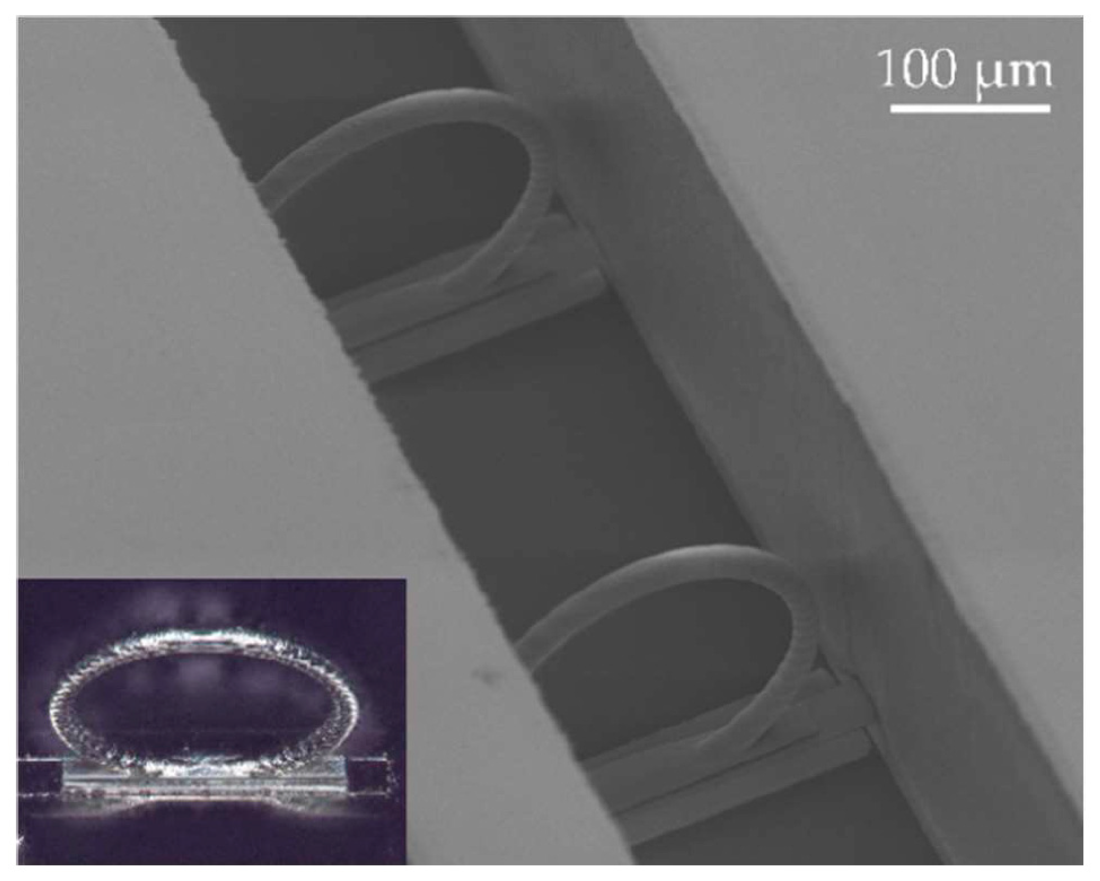
To test the quality of sputtering on 2PP structures, conductivity tests were performed beforehand. By applying contact probes, the conductivity between the top of the metallized structure and the bottom of the wafer was measured so that it is concluded that sputtering can be used to metallize 3D structures with good step coverage. Moreover, a 300 µm thick SU-8 layer can be applied on a wafer with only one spin-coating step. The SU-8 surface is smooth and the uniformity of the layer is 300 µm ± 10%, determined via laser scanning microscopy. Figure 2 shows an SEM picture of the ring structures after metallization and lift-off. A successful lift-off was confirmed using conductivity tests; by applying probes on top of both electrodes, no electrical connection could be measured. The channel’s bottom and the metal on the SU-8 are isolated from each other as well. As the next step, we will use this process for the realization of 3D dielectrophoresis devices.
Author Contributions
Conceptualization, W.G. and M.J.V.; investigation, W.G. and M.K.; writing—original draft preparation, W.G.; writing—review and editing, M.J.V. and M.K. All authors have read and agreed to the published version of the manuscript.
Funding
This research received no external funding.
Institutional Review Board Statement
Not applicable.
Informed Consent Statement
Not applicable.
Data Availability Statement
Data is contained within the article.
Conflicts of Interest
The authors declare no conflicts of interest.
References
- Aksit, A.; Rastogi, S.; Nadal, M.L.; Parker, A.M.; Lalwani, A.K.; West, A.C.; Kysar, J.W. Drug delivery device for the inner ear: Ultra-sharp fully metallic microneedles. Drug Deliv. Transl. Res. 2021, 11, 214–226. [Google Scholar] [CrossRef]
- Juarez, T.; Schroer, A.; Schwaiger, R.; Hodge, A.M. Evaluating sputter deposited metal coatings on 3D printed polymer micro-truss structures. Mater. Des. 2018, 140, 442–450. [Google Scholar] [CrossRef]
- Reede, S.; Bunge, F.; Oellers, M.; Vellekoop, M.J. A Process to Realize Direct Laser Written Electrostatic Actuator Elements in a Closed Microcavity. In Proceedings of the 2019 20th International Conference on Solid-State Sensors, Actuators and Microsystems & Eurosensors XXXIII (TRANSDUCERS & EUROSENSORS XXXIII), Berlin, Germany, 23–27 June 2019; pp. 106–109. [Google Scholar]
Figure 1.
Process to realize 2PP-based electrodes in a 300 μm high and wide channel.
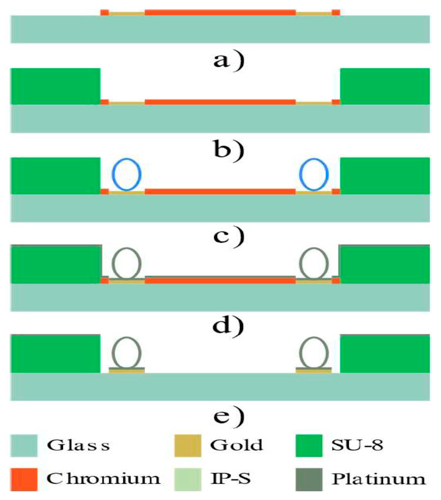
Figure 2.
2PP ring structures in a 300 μm high SU-8 channel after metallization and lift-off. Ring diameter is 250 μm, thickness 25 μm. The metal on the electrode is visible with digital microscopy (bottom left).
Figure 2.
2PP ring structures in a 300 μm high SU-8 channel after metallization and lift-off. Ring diameter is 250 μm, thickness 25 μm. The metal on the electrode is visible with digital microscopy (bottom left).
Disclaimer/Publisher’s Note: The statements, opinions and data contained in all publications are solely those of the individual author(s) and contributor(s) and not of MDPI and/or the editor(s). MDPI and/or the editor(s) disclaim responsibility for any injury to people or property resulting from any ideas, methods, instructions or products referred to in the content. |
© 2024 by the authors. Licensee MDPI, Basel, Switzerland. This article is an open access article distributed under the terms and conditions of the Creative Commons Attribution (CC BY) license (https://creativecommons.org/licenses/by/4.0/).
Share and Cite
MDPI and ACS Style
Gehlken, W.; Kirsch, M.; Vellekoop, M.J. A Process to Realize 2PP-Based Electrodes in Microfluidic Channels. Proceedings 2024, 97, 12. https://doi.org/10.3390/proceedings2024097012
AMA Style
Gehlken W, Kirsch M, Vellekoop MJ. A Process to Realize 2PP-Based Electrodes in Microfluidic Channels. Proceedings. 2024; 97(1):12. https://doi.org/10.3390/proceedings2024097012
Chicago/Turabian StyleGehlken, Wiebke, Melanie Kirsch, and Michael J. Vellekoop. 2024. "A Process to Realize 2PP-Based Electrodes in Microfluidic Channels" Proceedings 97, no. 1: 12. https://doi.org/10.3390/proceedings2024097012