
Etching and Compositional Ratio Effect on the Surface Properties of Bismuth Telluride Thin Films
by
 ,
,
Jeongho Mun
1,
Sangmin Han
1,
Hee-Seung Yoon
1,
Jisoo Kang
2,
Oliver Jonas
2,3,
Juyun Park
1 and
Yong-Cheol Kang
1,* 1
BB21 Plus Program, Department of Chemistry, Pukyong National University, Busan 48513, Republic of Korea
2
Department of Radiology, Brigham and Women’s Hospital, Boston, MA 02115, USA
3
Harvard Medical School, Harvard University, Boston, MA 02115, USA
*
Author to whom correspondence should be addressed.
Surfaces 2024, 7(1), 181-195; https://doi.org/10.3390/surfaces7010012
Submission received: 14 February 2024
/
Revised: 6 March 2024
/
Accepted: 11 March 2024
/
Published: 15 March 2024
(This article belongs to the Collection Featured Articles for Surfaces)
Abstract
:Bismuth telluride has garnered considerable attention owing to its versatile properties applicable in thermoelectric and antibacterial domains, as well as its intriguing topological insulating properties. In this work, our group fabricated bismuth telluride thin films with various ratios using radio frequency magnetron sputtering. The surface properties of these thin films were thoroughly analyzed by employing a diverse array of analytical techniques, including X-ray photoelectron spectroscopy (XPS), ultraviolet photoelectron spectroscopy (UPS), scanning electron microscopy (SEM), atomic force microscopy (AFM), X-ray diffraction (XRD), four-point probe and contact angle (CA) measurements. Specifically, our XPS findings indicated that Bi is more susceptible to oxidation than Te following Ar+-ion etching. Pure Te thin films exhibited the highest Rq value of 31.2 nm based on AFM and SEM results due to their larger grain sizes. The XRD patterns revealed a peak at 27.75° for thin films with 20% Te, attributed to its rhombohedral structure. Moreover, thin films with 30% Te yielded the highest weighted average work function with a value of 4.95 eV after etching. Additionally, pristine Bi and Te thin films demonstrated the most robust hydrophobic properties compared to intermediate-composition thin films, as determined by CA measurements.
1. Introduction
Chalcogenide materials such as GeTe and PbTe are known to exhibit remarkable thermoelectric properties [1,2]. Out of the many chalcogenide materials, bismuth telluride is a material that has been attracting recent interest due to its high thermoelectric performance at room temperature (RT) [3] and strong prospects for being incorporated in antibacterial and antimicrobial applications [4,5]. To elaborate, the material has a figure of merit value (Z) smaller than two at RT and a narrow bandgap (0.15 eV), and it is capable of turning waste heat into usable heat, thereby facilitating its usage in a variety of applications not limited to thermoelectric generators, sensors, microelectronics, antibacterial wound-healing biomaterials and aerodynamics [3,4,5,6,7,8,9]. Moreover, bismuth telluride has been reported to be a topological insulator, whose conducting surface states were revealed and isolated at thicknesses in a nanoscale regime, rendering the material an excellent system for further investigation to study quantum states [9,10,11]. However, studies of bismuth telluride nanomaterials with various Bi and Te composition ratios at RT and the pertaining physicochemical properties have not been conducted in detail. Therefore, providing this knowledge could be useful for promoting more sophisticated investigations regarding this material.
Thin films (TFs) are one of the many nanomaterials whose shape of the surface or element of oxidation can be controlled relatively easily along with a high surface-to-volume ratio [12,13]. There are many fabrication methods available to produce TFs, such as radio frequency (RF) magnetron sputtering, thermal evaporation, pulsed laser deposition, molecular beam epitaxy and electrochemical deposition [14,15,16,17,18,19]. Specifically, the RF magnetron co-sputtering method can easily adjust the atomic composition ratio by sending different powers to the two targets. Furthermore, the technique provides advantages such as high deposition rates and excellent adhesion between the TF material and substrate [20]. Thus, bismuth telluride TFs of various Te composition ratios were fabricated using the RF magnetron co-sputtering method and the resulting TFs were used as a platform to probe the surface properties in this work.
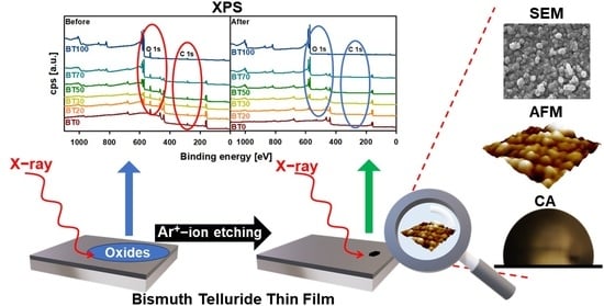
By examining the surface physicochemical properties of the TFs, changes in elementals oxidation state on the surface, where reactions occur faster than in bulk, can be applied in various nanoscale units. In this study, the chemical and photoelectric properties of BiTe TFs were investigated by XPS and UPS. The surface morphological properties were investigated by SEM, AFM and energy-dispersive X-ray spectroscopy (EDX). The crystallinity was investigated with XRD and electrical conductivity was investigated with a four-point probe. Finally, the wettability of the TFs’ surface and surface free energy were confirmed through CA measurements. In addition, XPS and UPS were measured to compare the differences in in situ situations by etching the surface with Ar+-ion.
2. Materials and Methods
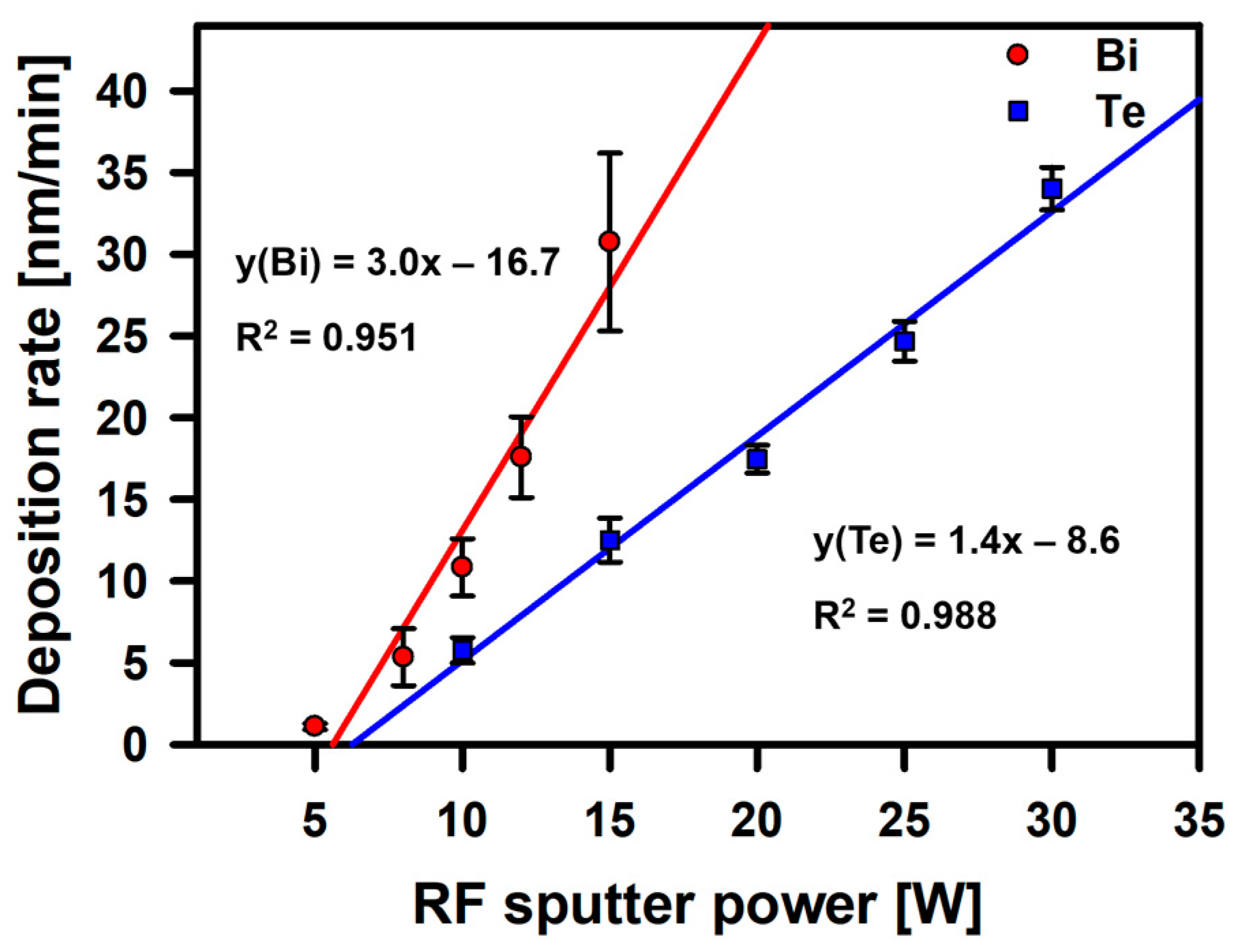
BiTe TFs were fabricated by RF magnetron co-sputtering in a high-vacuum sputtering chamber. The high vacuum was achieved by two rotary vane pumps (RPs) and a turbomolecular pump (TMP). In the chamber, Bi and Te (99.99%; Vacuum Thin Film Materials, Incheon, Republic of Korea) targets were inserted to fabricate BiTe thin films (TFs). Three targets are inserted in a triangular shape with equal spacing. Out of the three, two were ultimately used. P-type Si wafers were used as substrates for the TFs. The base pressure of the co-sputtering chamber was maintained at 2.4 × 10⁻² Pa. As the target was fixed, the Si substrates were rotated counterclockwise at 5 rpm using a sample rotator for uniform deposition of the TFs. The target temperature was maintained at 282 K using a water-cooled chiller. The Ar (99.999%; DONGIL, Gimhae, Republic of Korea) gas was used as a sputter gas, which was injected at a flow rate of 5 sccm (cm3/min) using a mass flow controller. Before co-sputtering, the target surface was cleaned via a plasma source, which was stabilized during the pre-sputtering process. Pre-sputtering was performed at a pressure of 5.33 Pa for 10 min at 20 (Bi) and 30 W (Te). Note that these RF powers are higher in value compared to the co-sputtering, which was performed at 1.33 Pa. To fabricate the BiTe TFs with the desired atomic ratios and thicknesses, we controlled the RF powers applied on the Bi and Te target and co-sputtering time. Figure 1 shows the deposition rates of pure Bi and Te thin films based on the RF sputtering power. The difference in the standard deviation values between Bi and Te is correlated to the higher power of Bi’s surface profile, resulting in the greater height deviation. The equations in Figure 1 describe the relationship between the thin film thickness and RF power. Table 1 shows the applied RF power and co-sputtering time for the BiTe TFs with various compositional ratios. In this paper, the sample will be characterized using the following notation: BTX, where X denotes the average value of the atomic percentages of Te in the BiTe TFs analyzed by EDX.
The average thickness of the fabricated TFs was about 229.3 ± 39.4 nm, which was measured with a surface profiler (Alpha-Step 500; Tencor, Milpitas, CA, USA). Relative atomic ratio and oxidation states of the TFs were investigated by X-ray photoelectron spectroscopy (XPS; KRATOS Analytical Ltd., Manchester, UK). XPS analysis was performed in an ultrahigh vacuum (UHV) chamber through RP and TMP. The base pressure of the XPS system was maintained at 2.0 × 10⁻⁸ Pa through RPs and TMPs. The X-ray source was AlKa (1486.6 eV) and 15 mA of emission current was used. The XPS spectra were obtained in two modes: survey and narrow spectra. The narrow spectra were monitored with 0.05 eV of step voltage for a high resolution and the survey spectra were obtained with 0.5 eV of step voltage. The obtained XPS spectra were deconvoluted with XPS peak4.1 software using a 30% Lorentzian–Gaussian ratio to identify the oxidation states of the elements in the BTX TFs. The surface of the TFs was in situ Ar+-ion-etched under the following conditions in the XPS vacuum chamber: the acceleration voltage of the Ar+-ion was set at 5 keV, the raster size at 9.00 mm2 and the etching time at 100 s. The etch rate was set to 0.085 nm/sec based on Ta2O5. Scanning electron microscopy (SEM, MIRA3; TESCAN, Brno, Czech Republic) coupled with energy-dispersive X-ray spectroscopy (EDX, X-max 50; Oxford Instruments, Abingdon, UK) and atomic force microscopy (AFM, Dimension FastScan; Bruker, Billerica, MA, USA) were conducted to investigate the morphology, topography and elemental composition of the TFs. The crystallinity of the TFs was monitored by X-ray diffraction (XRD, X`Pert3-Powder; Malvern Panalytical, Malvern, UK) using a Cu Kα source with 40.0 kV of acceleration voltage and 40.0 mA of filament current. To obtain the work function (WF) of the TFs, ultraviolet photoelectron spectroscopy (UPS; KRATOS Analytical Ltd., Manchester, UK) and a Kelvin probe (KP, KP6500; McAllister Technical Services, Coeur d’Alene, ID, USA) were utilized. The source used for UPS was HeI (21.2 eV) operating at a bias of −9 V. For KP, pure Au (99.99%; MADE LAB, Hanam, Republic of Korea) metal was used as a reference. The electrical properties of TFs were measured using a 4-point probe system (Loresta-GP MCP-T600; Mitsubishi Chemical, Kanagawa, Japan). The surface free energy of the BTX TFs was investigated with distilled water (DW) and ethylene glycol (EG) by using a homemade contact angle (CA) measurement system. The experimental details are described elsewhere [21].
3. Results and Discussion
Table 2 shows the relative atomic percentages of Bi and Te in the BTX TFs determined by the XPS and EDX results. The contents of Bi decreased as Te increased in both the XPS and EDX results. It was confirmed that the different compositional ratios of BTX TFs were successfully fabricated by adjusting the RF power on the Bi and Te targets as listed in Table 1. The differences in the two values (XPS vs. EDX) are likely ascribed to the TF surface region mainly contributing to the XPS signal while the bulk region mainly contributes to the EDX signal [22,23]. To elaborate, Te, which was predominately located in the bulk, would gradually proceed to relocate to the surface side as oxidation proceeded, resulting in a ratio difference compared to the bulk. In the case of BT20, the relative atomic percentage of Te detected by XPS was higher than Te by EDX. This special case implies that Te preferentially exists on the surface region rather than in the bulk region at this particular ratio, because BT20 has the smallest composition ratio of Te, thus leading to relatively fewer Te atoms to form Bi2Te3, ultimately causing the formation of Bi2Te3 as a less feasible option along with oxidation occurring on the surface.
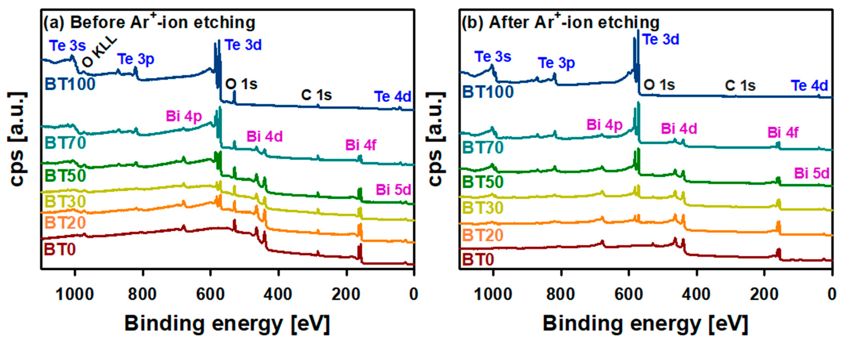
We examined the effect of Ar+-ion etching on the surface characteristics. The XPS survey spectra of the BTX TFs with various atomic ratios before and after Ar+-ion etching are shown in Figure 2a,b, respectively. All spectra were calibrated based on the binding energy of adventitious C 1s at 284.6 eV [24,25,26]. In the XPS survey spectra, the characteristic peaks of Bi and Te were detected. As the contents of Te increased, the peak intensity of Bi decreased as expected as shown in Figure 2. From this step, we again confirmed that the BTX TFs with various atomic ratios were successfully fabricated by the RF magnetron co-sputtering method. Interestingly, in Figure 2a, oxygen and carbon peaks as surface contaminants were detected as well. However, after Ar+-ion etching was performed, the peak intensities of oxygen and carbon were significantly reduced, as shown in Figure 2b. From these results, we confirmed that the surface contaminants including carbon oxides were removed effectively through the Ar+-ion etching. The relative atomic percentages of Bi, Te and O on the surface region of the BTX TFs obtained by XPS before and after Ar+-ion etching are listed in Table 3. The oxygen percentages decreased significantly by 40~50% for all BTX TFs after Ar+-ion etching, while the Bi and Te percentages increased.
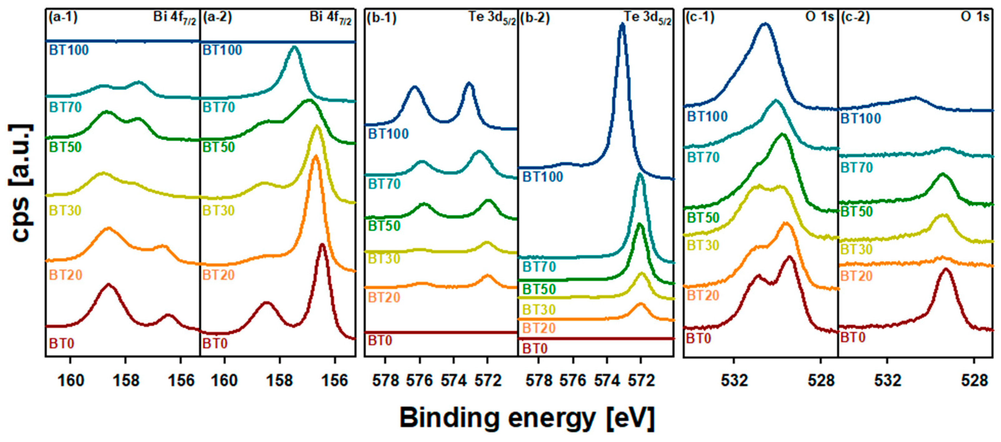
The narrow XPS spectra of Bi 4f7/2, Te 3d5/2 and O 1s of the BTX TFs before Ar+-ion etching are shown in Figure 3(a-1–c-1), respectively. The narrow XPS spectra of Bi 4f7/2, Te 3d5/2 and O 1s after Ar+-ion etching are shown in Figure 3(a-2–c-2), respectively. The peak profiles of Bi, Te and O evolved after Ar+-ion sputtering, as shown in Figure 3. This evolution indicates that the atomic ratio of the chemical species of different oxidation states for each element changed drastically. In order to obtain the detailed chemical information of Bi, Te and O, the narrow XPS spectra were deconvoluted with XPS peak4.1 and the detailed fitting parameters are described elsewhere [20]. To avoid the complexity during the peak fitting process due to the large spin orbit-splitting constants of Bi 4f (5.4 eV) and Te 3d (10.4 eV) [27,28], Bi 4f7/2 and Te 3d5/2 peaks were deconvoluted instead of the whole Bi 4f and Te 3d peaks. The representative deconvoluted XPS spectra of Bi 4f7/2, Te 3d5/2 and O 1s of BTX TFs before Ar+-ion etching are shown in Figure 4(a-1–c-1), respectively. The representative deconvoluted XPS spectra of Bi 4f7/2, Te 3d5/2 and O 1s after Ar+-ion etching are shown in Figure 4(a-2–c-2), respectively. The peak intensity of oxygen decreased while Bi and Te increased after Ar+-ion etching, as shown in Figure 4. The decrease in the O 1s peak is likely associated with the removal of surface contaminants such as H2O and carbonyl group by Ar+-ion etching. The increase in the Bi and Te peaks heavily implies that Bi and Te were exposed on the surface region after the removal of surface contaminants by Ar+-ion etching.
The deconvoluted Bi 4f7/2 peaks were assigned to metallic Bi (Bi0) at 158.6 eV, Bi2Te3 (Bi3+–Te2–) at 157.6 eV, and oxidized Bi (Bi2+–O and Bi3+–O) at 157.1 and 158.7 eV, respectively [29,30,31,32,33]. The deconvoluted Te 3d5/2 peaks were assigned to metallic Te (Te0) at 572.9 eV, Bi2Te3 (Te2––Bi3+) at 572.1 eV, and oxidized Te (Te6+–O, Te4+–O, Te2+–O) at 576.8, 575.9, and 574.0 eV, respectively [34,35,36,37,38,39]. The deconvoluted O 1s peaks were assigned to H2O at 532.2 eV, C=O at 531.1 eV, Te–O at 530.3 eV, Bi3+–O at 529.7, and Bi2+–O at 529.2 eV [40,41,42,43,44].
The relative atomic ratios of Bi, Te and O with different oxidation states before and after Ar+-ion etching are shown in Figure 5(a-1–c-2), respectively. These values were obtained by applying the atomic sensitivity factors of Bi 4f7/2, Te 3d5/2 and O 1s as 4.25, 5.40 and 0.66, respectively [45,46,47].
Comparing the oxide ratios of Bi and Te before Ar+-ion etching, it can be seen that Bi was more readily oxidized than Te, as shown in Figure 5(a-1,b-1). A plausible explanation for this is that Bi has a smaller electronegativity of 2.02 than Te of 2.10 on the Pauling scale [48,49]. Before Ar+-ion etching, Bi oxides and Te oxides were the major chemical species of Bi and Te, respectively. However, after Ar+-ion etching as shown in Figure 5(a-2,b-2), most of the oxides of Bi and Te were removed. Thus, after Ar+-ion etching, Bi0 and Bi3+–Te2– peaks became the most established peaks of Bi, while Te0 and Bi–Te2– peaks became the most established peaks of Te. Moreover, in Table 1, as the Te composition ratio increased, the power increased accordingly. The calculated Te power/Bi power is tabulated in Table 4, and the trend indicates that the Bi–Te bond increased as well from 1.25 to 1.67. Furthermore, the intensity of the Bi2Te3 peak also increased with this trend as shown in Figure 5.
UPS was employed to determine the WFs of the BTX TFs. The WFs were computed utilizing the following equation [7]:
WF = 21.2 eV (He I) − (Fermi level − secondary cutoff).
The obtained WF values before and after Ar+-ion etching are shown in Figure 6a,b, respectively. Figure 7 shows the atomic percentages of Bi and Te species with different oxidation states. Intuitively, the expected propensity of WF was thought to increase as the contents of Te increased because the WFs of Te and bismuth telluride were reported with higher values than Bi [50,51]. The reported WF values of Bi, Te, Bi oxide and Te oxide are listed in Table 5 [50,51,52,53,54]. In other words, the WFs were expected to be BT70 > BT50 > BT30 > and BT20; however, our experimental findings deviated from such anticipation. As displayed in Figure 4, the XPS results revealed that numerous Bi and Te species with different oxidation states existed in the BTX TFs. These Bi and Te oxides contributed to the WF of the BTX TFs. Therefore, the weighted average WF was calculated considering the obtained atomic percentages of chemical species with different oxidation states. Table 6 lists the relative atomic percentages of chemical species with oxidation states of the BTX TFs and the obtained weighted average WFs of the corresponding TFs. For instance, in the case of BT20, the weighted average WF was calculated as [(19.6 × 4.64 eV) + (1.90 × 4.80 eV) + (59.8 × 5.07 eV) + (18.6 × 4.20 eV)]/100 = 4.81 eV. However, as shown in Figure 4, most of the oxide species were removed after Ar+-ion etching. Therefore, it was expected that the WFs after Ar+-ion etching would fit with the estimated tendency. The WF values from after Ar+-ion etching BTX TFs were plotted as Figure 6b. As expected, the WF increased as the ratio of Te increased in the order of BT20, BT30, BT50 and BT70, and then it decreased to 4.86 eV in BT100 (pure Te).
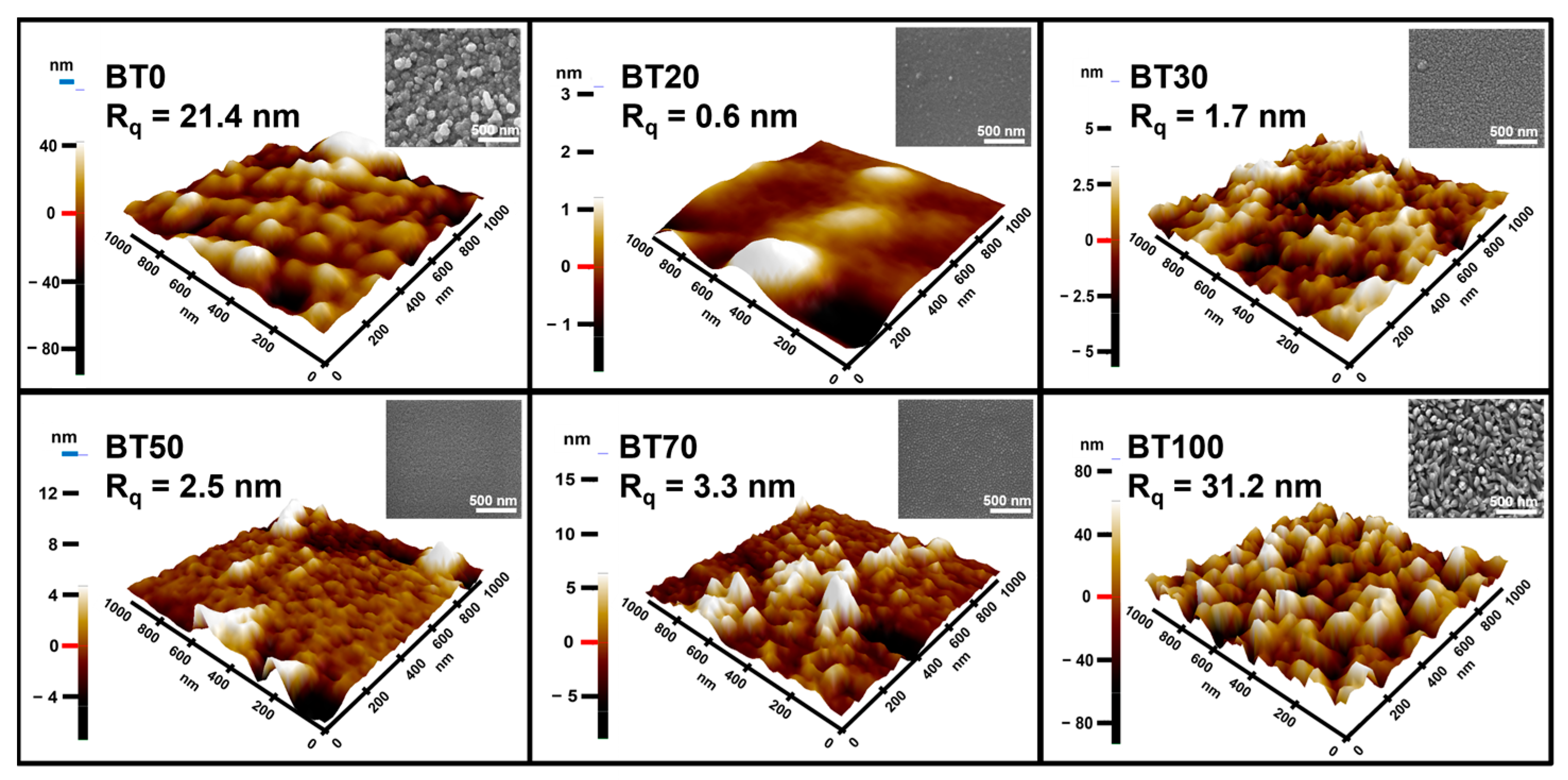
Figure 8 shows the surface morphologies of the BTX TFs obtained by SEM (inset) and topological images monitored by AFM. The SEM micrographs were magnified by 150 k. Interestingly, some grains were identified only in pure TFs such as BT0 and BT100. Other BTX TFs showed a relatively smooth surface without distinct grains in the SEM micrographs. The roughness of the TFs is expressed as Rq, which is the root mean squared value obtained from our AFM measurements. The results showed large Rq values in BT0 and BT100 due to their specific grain shapes identified in the SEM, and smaller Rq values were obtained in BT20 to BT70, rather than in BT0 and BT100. The large Rq values in BT0 and BT100 could be ascribed to TFs growing in an island shape elucidated by the Volmer–Webber growth mechanism [55,56]. According to JCPDS No. 85–1331, 86–2269, 82–0358 and 77–2109, the lattice parameters were a = 4.533 for Bi, a = 4.454 for Te, a = 4.395 for Bi2Te3, and a = 5.418 for Si (substrate). The lattice mismatch was calculated using Equation (2), given below as the following:
where a0(s) is the lattice parameter of the substrate and a1(f) is the parameter of the deposited material. The calculated lattice mismatch value was f = 0.195 for Bi, f = 0.216 for Te and f = 0.233 for Bi2Te3. If the f value is less than 0.09, it is known that the film grows in accordance to the lattice of the substrate. However, Bi, Te and Bi2Te3 all have values higher than 0.09, so it can be considered that it grew into an island form. The Rq values of BT20 through BT70 were smaller than for BT0 and BT100, while the Rq values increased from BT20 to BT70. From these observations, we can conclude that Te had a stronger influence on the surface roughness of the BTX TFs than Bi.
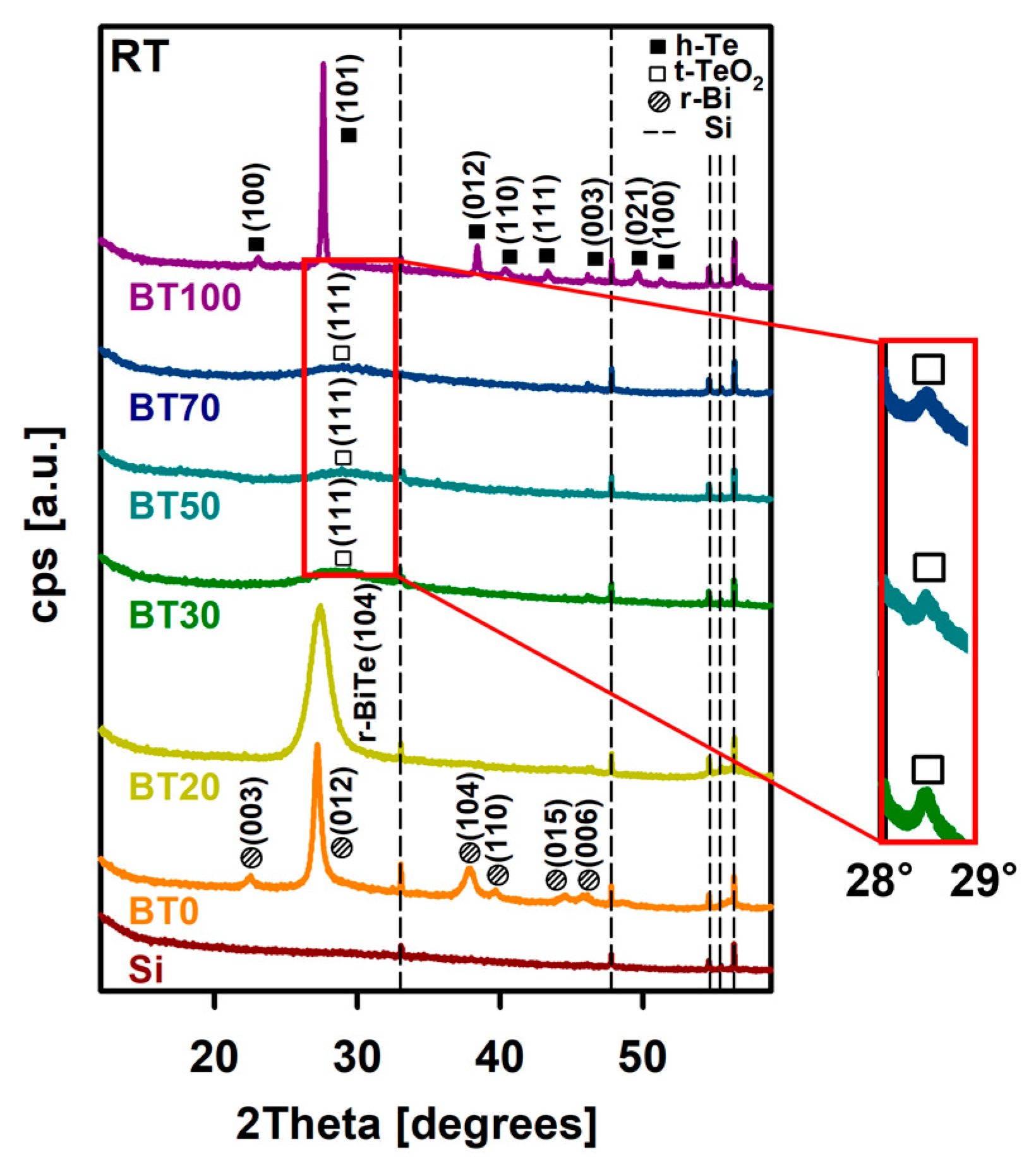
Figure 9 shows the XRD patterns of the BTX TFs. The peaks in BT0 were observed at the diffraction angles of 22.59°, 27.27°, 38.14°, 39.74°, 44.78° and 46.13° (JCPDS No. 85–1331). These characteristic peaks pertain to the rhombohedral Bi phases [57]. In BT20, a peak at 27.75° (JCPDS No. 82–0358) was observed and assigned to the rhombohedral BiTe peak. In the BT30, BT50 and BT70 TFs, a peak at 28.74° (JCPDS No. 84–1777) was detected and assigned to the tetrahedral TeO2 peak. In BT100, peaks at 23.04°, 27.58°, 38.28°, 43.47°, 45.09°, 49.67°, 51.28° and 56.93° (JCPDS No. 86–2269) were observed and assigned to the phases of hexagonal Te [58]. In other bismuth telluride thin film studies, when the thin film was fabricated and annealed at a power exceeding 15 W (Bi) and 30 W (Te) (the highest power we set in our experiment), many peaks did not appear even at 100 °C. As the temperature increases, various peaks appear with increased intensities [59,60]. Comparing such results with previous studies, the formation conditions of BTX TFs in this work were insufficient to form a crystalline structure. Therefore, it was difficult to observe crystal peaks in the BT20 through BT70 TFs [59,60]. Additionally, the lattice strain was measured using the Williamson–Hall equation:
where β is the full width at half maximum of the diffraction peaks, θ is Bragg’s angle, K is the constant 0.9, λ is the wavelength of X-ray radiation (CuKα = 0.15406 nm), τ is the crystallite size (nm) and ε is the strain of the sample. Using the θ and β values shown in Table 7, a graph was constructed with 4sinθ on the x-axis and βcosθ on the y-axis, in which the slope is expressed as ε.
The calculated lattice strain values were found to be the following: r-Bi of 1.70 × 10⁻³ and h-Te of 3.00 × 10⁻³. The bond length of Bi was 2.90 ~ 3.07 Å and of Te, 2.74 Å. In addition, the electronegativity was 2.02 for Bi and 2.10 for Te, which is relatively larger than Bi and a shorter bond length, so it can be seen that the bonds between Te were stronger than for Bi. Moreover, as seen in Figure 8, the morphology of BT100 was sharper and denser in grains than BT0. Through these points, it can be seen that Te, which had a larger strain value, received more stress than Bi, and thus, the surface roughness value was also larger. In addition, there was another study that showed a proportional relationship between surface roughness and strain [61].
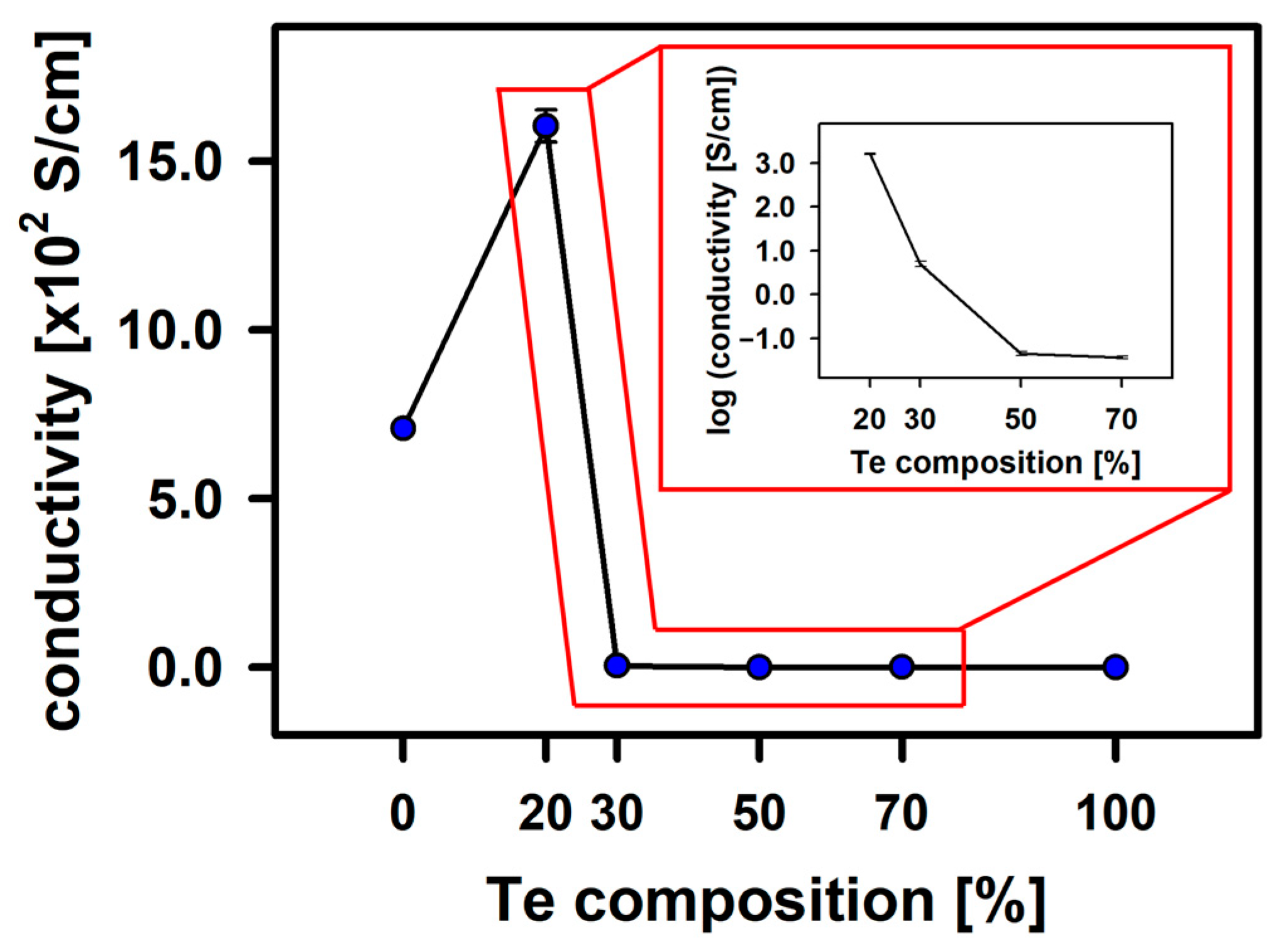
Figure 10 shows the electrical conductivity of the BTX TFs measured by a four-point probe as a function of Te composition. Note that the scale of the ordinate of the inset is in log scale of the conductivity. Firstly, Bi is a metallic element while Te is a metalloid; thus, the electrical conductivity value of BT0 is relatively higher than BT100 [62,63]. Therefore, as the ratio of Te increases, the electrical conductivity of the BTX TFs should have tended to decrease. Surprisingly, BT20 showed higher electrical conductivity than BT0. This unexpected result could be related to the discontinuity and roughness of the TFs’ surface. The lower the continuity and rougher the surface of TFs, the lower the electrical conductivity [64]. Interestingly, there have been reports of a correlation between roughness and electrical conductivity, hinting at possibilities of topological insulation effects due to Bi2Te3 being a topological insulator [9]. From the AFM data, as shown in Figure 8, BT20 showed a smaller roughness (0.6 nm) than BT0 (21.4 nm). The grain boundaries, which caused the discontinuity of the TFs, formed in higher quantities in BT0 than in BT20, as shown in the SEM micrographs in Figure 8. These two factors contributed to the higher electrical conductivity in BT20 than in BT0. In order to accurately characterize the trend of the electrical conductivities from BT20 to BT70, the scale of the ordinate was taken as the logarithm of the conductivity, and it is shown in the inset of Figure 10. Clearly, as the ratio of Te increased, the electrical conductivity tended to decrease. As seen in the AFM data, as shown in Figure 8, the Rq value increased as Te increased and the electrical conductivity tended to decrease due to the increase in Rq.
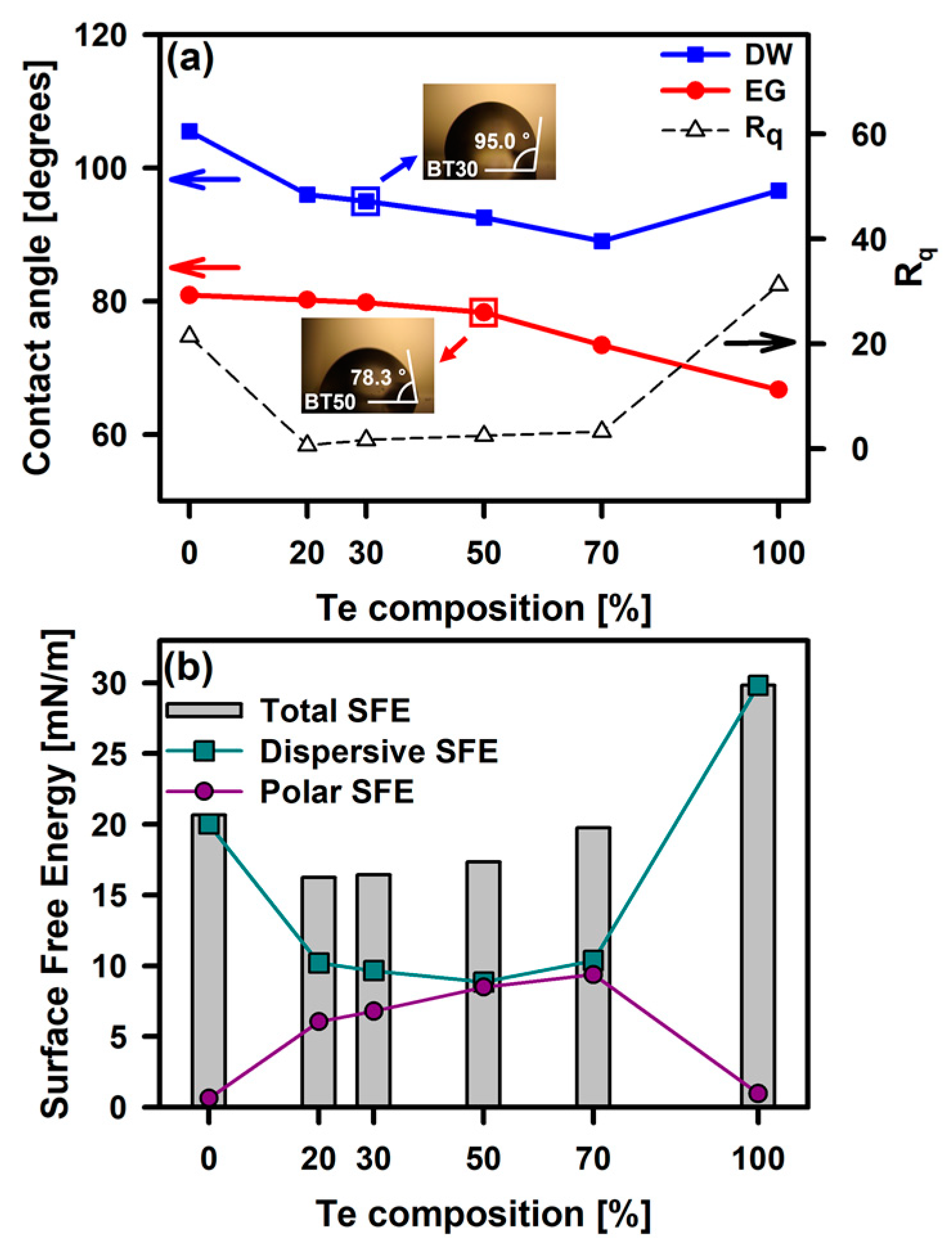
Figure 11a shows the roughness of the BTX TFs and the CA, measured by dropping 2 μL DW and EG. Figure 11b presents the calculated dispersive, polar and total SFE values of the TFs which were calculated by using the modified Young’s equation by Owens and Wendt with the measured CA values. The modified Young’s equation is described as
where is the surface tension of the used liquids (DW and EG) and is the contact angle between the BTX TFs and the liquid. The and are the surface tensions of the dispersive and polar components of the TFs, respectively. The and are the surface tensions of the dispersive and polar component of the liquids, respectively. The calculated SFE values are listed in Table 8.
The pure TFs such as BT0 and BT100 showed strong hydrophobic properties because the dispersive SFE is larger than the polar SFE, as shown in Figure 11b. On the other hand, the mixed TFs such as BT20, BT30, BT50 and BT70 still had a higher dispersive SFE, but the polar SFE increased significantly. As the compositional ratio of Te increased, the polar SFE increased. The tendency of the total SFEs was similar to that of the roughness of the TFs determined in our AFM measurements.
4. Conclusions
In conclusion, bismuth telluride thin films of various ratios were successfully fabricated by employing RF magnetron sputtering. The surface properties of the fabricated films were characterized by utilizing a wide range of analytical techniques such as XPS, SEM, AFM, XRD, four-point probe, UPS and CA measurements. To elaborate, the XPS results revealed that Bi is more prone to oxidation than Te after Ar+-ion etching; pristine Bi and Te thin films yielded the highest Rq values (21.4 nm and 31.2 nm, respectively) from the AFM and SEM results due to their large grain sizes; BT20 exhibited a peak at 27.75° due to its rhombohedral structure from the XRD patterns; the electrical conductivity of the thin films tended to decrease with increasing Te concentration; and pristine Bi and Te thin films showed the strongest hydrophobic nature compared to the other thin films based on the CA measurements. We hope that our findings promote further investigations regarding bismuth telluride materials in studying their thermoelectric, topologically insulating and even antimicrobial properties.
Author Contributions
Conceptualization, Y.-C.K. and J.P.; methodology, Y.-C.K. and J.M.; validation, Y.-C.K. and S.H.; formal analysis, H.-S.Y.; investigation, J.M. and Y.-C.K.; data curation, J.K.; writing—original draft preparation, J.M.; writing—review and editing, J.K., Y.-C.K. and O.J.; supervision, Y.-C.K. All authors have read and agreed to the published version of the manuscript.
Funding
This research received no external funding.
Institutional Review Board Statement
Not applicable.
Informed Consent Statement
Not applicable.
Data Availability Statement
The data presented in this study are available in this article.
Conflicts of Interest
The authors declare no conflict of interest.
References
- Ishibe, T.; Komatsubara, Y.; Ishikawa, K.; Takigawa, S.; Naruse, N.; Mera, Y.; Yamashita, Y.; Ohishi, Y.; Nakamura, Y. Boosting Thermoelectric Performance in Epitaxial GeTe Film/Si by Domain Engineering and Point Defect Control. ACS Appl. Mater. Interfaces 2023, 15, 26104. [Google Scholar] [CrossRef]
- Han, C.; Tan, G.; Varghese, T.; Kanatzidis, M.G.; Zhang, Y. High-Performance PbTe Thermoelectric Films by Scalable and Low-Cost Printing. ACS Energy Lett. 2018, 3, 818–822. [Google Scholar] [CrossRef]
- El-Makaty, F.M.; Ahmed, H.K.; Youssef, K.M. The Effect of Different Nanofiller Materials on the Thermoelectric Behavior of Bismuth Telluride. Mater. Des. 2021, 209, 109974. [Google Scholar] [CrossRef]
- Nour, A.; Hamida, R.S.; El-Dissouky, A.; Soliman, H.M.A.; Refaat, H.M. One-Pot Facile Synthesis of Hexagonal Bi2Te3 Nanosheets and Its Novel Nanocomposites: Characterization, Anticancer, Antibacterial, and Antioxidant Activities. Colloids Surf. B 2023, 225, 113230. [Google Scholar] [CrossRef] [PubMed]
- Liu, X.; Ma, L.; Chen, F.; Liu, J. Synergistic Antibacterial Mechanism of Bi2Te3 Nanoparticles Combined with Ineffective β-Lactam Antibiotic Cefotaxime Against Methicillin-Resistant Staphylococcus aureus. J. Inorg. Biochem. 2019, 196, 110687. [Google Scholar] [CrossRef] [PubMed]
- Cao, T.; Shi, X.-L.; Li, M.; Hu, B.; Chen, W.; Liu, W.-D.; Lyu, W.; MacLeod, J.; Chen, Z.-G. Advances in Bismuth-Telluride-based Thermoelectric Devices: Progress and Challenges. eScience 2023, 3, 100122. [Google Scholar] [CrossRef]
- Mamur, H.; Bhuiyan, M.R.A.; Korkmaz, F.; Nil, M. A Review on Bismuth Telluride (Bi2Te3) Nanostructure for Thermoelectric Applications. Renew. Sustain. Energy Rev. 2018, 82, 4159–4169. [Google Scholar] [CrossRef]
- Chen, R.; Wei, L.; Yan, Y.; Chen, G.; Yang, X.; Liu, Y.; Zhang, M.; Liu, X.; Cheng, Y.; Sun, J.; et al. Bismuth Telluride Functionalized Bismuth Oxychloride Used for Enhancing Antibacterial Activity and Wound Healing Efficacy with Sunlight Irradiation. Biomater. Sci. 2022, 10, 467–473. [Google Scholar] [CrossRef]
- Zhang, H.; Liu, C.X.; Qi, X.L.; Dai, X.; Fang, Z.; Zhang, S.C. Topological Insulators in Bi2Se3, Bi2Te3 and Sb2Te3 with a Single Dirac Cone on the Surface. Nat. Phys. 2009, 6, 438–442. [Google Scholar] [CrossRef]
- Steiner, H.; Volobuev, V.; Caha, O.; Bauer, G.; Springholz, G.; Holý, V. Structure and Composition of Bismuth Telluride Topological Insulators Grown by Molecular Beam Epitaxy. J. Appl. Crystallogr. 2014, 6, 1889–1900. [Google Scholar] [CrossRef]
- Ashalley, E.; Chen, H.; Tong, X.; Li, H.; Wang, Z.M. Bismuth Telluride Nanostructures: Preparation, Thermoelectric Properties and Topological Insulating Effect. Front. Mater. Sci. 2015, 9, 103–125. [Google Scholar] [CrossRef]
- Choi, S.; Kang, J.; Park, J.; Kang, Y.-C. Tin Nitride Thin Films Fabricated by Reactive Radio Frequency Magnetron Sputtering at Various Nitrogen Gas Ratios. Thin Solid Films 2014, 571, 84–89. [Google Scholar] [CrossRef]
- Choi, S.; Park, J.; Kang, J.; Johnson, A.T.C.; Kang, Y.-C. Surface Characterization of PZT Thin Films Obtained at Various O2 Gas Ratios. Vacuum 2016, 128, 234–239. [Google Scholar] [CrossRef]
- Zeng, Z.; Yang, P.; Hu, Z. Temperature and Size Effects on Electrical Properties and Thermoelectric Power of Bismuth Telluride Thin Films Deposited by Co-Sputtering. Appl. Surf. Sci. 2013, 268, 472–476. [Google Scholar] [CrossRef]
- Singkaselit, K.; Sakulkalavek, A.; Sakdanuphab, R. Effects of Annealing Temperature on the Structural, Mechanical and Electrical Properties of Flexible Bismuth Telluride Thin Films Prepared by High-Pressure RF Magnetron Sputtering. Adv. Nat. Sci. Nanosci. Nanotechnol. 2017, 8, 035002. [Google Scholar] [CrossRef]
- Rogacheva, E.I.; Budnik, A.V.; Dobrotvorskaya, M.V.; Fedorov, A.G.; Krivonogov, S.I.; Mateychenko, P.V.; Nashchekina, O.N.; Sipatov, A.Y. Growth and structure of thermally evaporated Bi2Te3 thin films. Thin Solid Films 2016, 612, 128–134. [Google Scholar] [CrossRef]
- Le, P.H.; Liao, C.-N.; Luo, C.W.; Leu, J. Thermoelectric Properties of Nanostructured Bismuth-Telluride Thin Films Grown Using Pulsed Laser Deposition. J. Alloys Compd. 2014, 615, 546–552. [Google Scholar] [CrossRef]
- Wang, Z.; Zhang, X.; Zeng, Z.; Hu, Z. Two-Step Molecular Beam Epitaxy Growth of Bismuth Telluride Nanoplate Thin Film with Enhanced Thermoelectric Properties. ECS Solid State Lett. 2014, 3, P99. [Google Scholar] [CrossRef]
- Golia, S.; Arora, M.; Sharma, R.K.; Rastogi, A.C. Electrochemically Deposited Bismuth Telluride Thin Films. Curr. Appl. Phys. 2003, 3, 195–197. [Google Scholar] [CrossRef]
- Choi, J.; Park, J.; Kang, J.; Kehayias, C.E.; Oh, J.W.; Kang, Y.-C. Annealing Temperature Effect on the Surface Properties of the MoSe Thin Films. Phys. Status Solidi A 2023, 220, 2300477. [Google Scholar] [CrossRef]
- Yoon, H.; Lee, J.; Park, J.; Oh, J.W.; Kang, Y.-C. Physicochemical Properties of SnTe Thin Films Dependent on Compositional Ratios. Phys. Status Solidi A 2022, 219, 2200059. [Google Scholar] [CrossRef]
- Stevie, F.A.; Garcia, R.; Shallenberger, J.; Newman, J.G.; Donley, C.L. Sample Handling, Preparation and Mounting for XPS and Other Surface Analytical Techniques. J. Vac. Sci. Technol. A 2020, 38, 063202. [Google Scholar] [CrossRef]
- Kim, D.; Park, J.; Choi, J.; Oh, J.W.; Kang, Y.-C. Compositional Ratio Effect on the Physicochemical Properties of SnSe Thin Films. Phys. B Condens. Matter 2021, 612, 412890. [Google Scholar] [CrossRef]
- Choi, A.; Park, J.; Kang, J.; Jonas, O.; Kim, D.; Kim, H.; Oh, J.W.; Kang, Y.-C. Surface Characterization and Investigation on Antibacterial Activity of CuZn Nanofibers Prepared by Electrospinning. Appl. Surf. Sci. 2020, 508, 144883. [Google Scholar] [CrossRef]
- Jeong, E.; Park, J.; Choi, S.; Kang, J.; Kang, Y.-C. Surface Characteristics of MoN x Thin Films Obtained by Reactive rf Magnetron Sputtering in UHV System. Bull. Korean Chem. Soc. 2015, 36, 2446. [Google Scholar] [CrossRef]
- Park, J.; Seo, S.Y.; Kang, Y.-C. Tuning the Oxidation States and Crystallinity of Copper Oxide Nanofibers by Calcination. J. Vac. Sci. Technol. B 2014, 32, 04E104. [Google Scholar] [CrossRef]
- Balakrishnan, R.; Dixit, A.; Rao, M.S.R.; Naik, R. Influence of Ca Doping on X-Ray Photoelectron Core-Level Spectra of Magnetoelectric Bulk BiFeO3. Surf. Interface Anal. 2021, 53, 798–807. [Google Scholar] [CrossRef]
- Soriano, L.; Galan, L.; Rueda, F. An XPS Study of Cs2Te Photocathode Materials. Surf. Interface Anal. 1990, 16, 193–198. [Google Scholar] [CrossRef]
- Qiao, Y.; Lai, W.; Huang, K.; Yu, T.; Wang, Q.; Gao, L.; Yang, Z.; Ma, Z.; Sun, T.; Liu, M.; et al. Engineering the Local Microenvironment over Bi Nanosheets for Highly Selective Electrocatalytic Conversion of CO2 to HCOOH in Strong Acid. ACS Catal. 2022, 12, 2357–2364. [Google Scholar] [CrossRef]
- Kogo, G.; Lee, H.; Ibrahim, A.H.; Bo, X.; Pradhan, S.K.; Bahoura, M. Highly-Efficient Thermoelectric PN-Junction Device based on Bismuth Telluride (Bi2Te3) and Molybdenum Disulfide (MoS2) Thin Films Fabricated by RF Magnetron Sputtering Technique. J. Appl. Phys. 2018, 124, 16. [Google Scholar] [CrossRef]
- Zhu, H.-T.; Luo, J.; Fan, H.-M.; Zhang, H.; Liang, J.-K.; Rao, G.-H.; Li, J.-B.; Liu, G.-Y.; Du, Z.-M. Tri-wing Bismuth Telluride Nanoribbons with Quasi-Periodic Rough Surfaces. J. Mater. Chem. 2011, 21, 12375–12380. [Google Scholar] [CrossRef]
- Hu, Y.; Chen, G.; Li, C.; Han, Z.; Hao, S.; Hong, W.; Xing, W. Non-Integer Induced Spontaneous Polarization of Highly Efficient Perovskite-based NBTO SCN Photocatalysts. J. Mater. Chem. A 2017, 5, 22984–22987. [Google Scholar] [CrossRef]
- Gomez-Iriarte, G.A.; Pentón-Madrigal, A.; de Oliveira, L.A.S.; Sinnecker, J.P. XPS Study in BiFeO3 Surface Modified by Argon Etching. Materials 2022, 15, 4285. [Google Scholar] [CrossRef] [PubMed]
- Shevchik, N.J.; Cardona, M.; Tejeda, J. X-Ray and Far-UV Photoemission from Amorphous and Crystalline Films of Se and Te. Phys. Rev. B 1973, 8, 2833. [Google Scholar] [CrossRef]
- Wang, Q.; Jiang, C.; Yu, C.; Chen, Q. General Solution-based Route to V-VI Semiconductors Nanorods from Hydrolysate. J. Nanopart. Res. 2007, 9, 269–274. [Google Scholar] [CrossRef]
- Zeng, C.; Ramos-Ruiz, A.; Field, J.A.; Sierra-Alvarez, R. Cadmium Telluride (CdTe) and Cadmium Selenide (CdSe) Leaching Behavior and Surface Chemistry in Response to pH and O2. J. Environ. Manag. 2015, 154, 78–85. [Google Scholar] [CrossRef]
- Wei, T.; Wei, J.; Zhang, K.; Zhang, L. Image Lithography in Telluride Suboxide Thin Film through Controlling “Virtual” Bandgap. Photon. Res. 2017, 5, 22–26. [Google Scholar] [CrossRef]
- Swartz, W.E.; Wynne, K.J.; Hercules, D.M. X-ray Photoelectron Spectroscopic Investigation of Group VIA Elements. Anal. Chem. 1971, 43, 1884–1887. [Google Scholar] [CrossRef]
- Bahl, M.K.; Watson, R.L.; Irgolic, K.J. X-ray Photoemission Studies of Telluride and Some of Its Compounds. J. Chem. Phys. 1977, 66, 5526. [Google Scholar] [CrossRef]
- Fan, K.; Ji, Y.; Zou, H.; Zhang, J.; Zhu, B.; Chen, H.; Daniel, Q.; Luo, Y.; Yu, J.; Sun, L. Hollow Iron-Vanadium Composite Spheres: A Highly Efficient Iron-based Water Oxidation Electrocatalyst without the Need for Nickel or Cobalt. Angew. Chem. Int. Ed. 2017, 56, 3289–3293. [Google Scholar] [CrossRef]
- Arteaga, G.; Rivera-Gavidia, L.M.; Martinez, S.J.; Rizo, R.; Pastor, E.; Garcia, G. Methanol Oxidation on Graphenic-supported Platinum Catalysts. Surfaces 2019, 2, 16–31. [Google Scholar] [CrossRef]
- Rinke, M.T.; Zhang, L.; Eckert, H. Structural Integration of Tellurium Oxide into Mixed-Network-Former Glasses: Connectivity Distribution in the System NaPO3-TeO2. ChemPhysChem 2007, 8, 1988–1998. [Google Scholar] [CrossRef]
- Chu, D.; Wu, Y.; Wang, L. Synthesis and Characterization of Novel Coral Spherical Bismuth Oxide. Results Chem. 2022, 4, 100448. [Google Scholar] [CrossRef]
- Li, J.; Wu, X.; Wan, Z.; Chen, H.; Zhang, G. Full Spectrum Light Driven Photocatalytic in-situ Epitaxy of One-Unit-Cell Bi2O2CO3 layers on Bi2O4 nanocrystals for Highly Efficient Photocatalysis and Mechanism Unveiling. Appl. Catal. B Environ. 2019, 243, 667–677. [Google Scholar] [CrossRef]
- Yu, M.; Peng, X.; Luo, Y.; Yin, S. Applying Research on Creep Constitutive Model of LC4 Aluminium Alloy Based on BC-RBFNN. J. Appl. Phys. 2010, 108, 083704. [Google Scholar]
- Bernede, J.C.; Alaoui, Z.K.; Manai, N. Films of Molybdenum Trioxide Obtained from MoTe2 Oriented Films. Thin Solid Films 1993, 235, 25–29. [Google Scholar] [CrossRef]
- Jensen, H.; Soloviev, A.; Li, Z.; Sogaard, E.G. XPS and FTIR Investigation of the Surface Properties of Different Prepared Titania Nano-Powders. Appl. Surf. Sci. 2005, 246, 239–249. [Google Scholar] [CrossRef]
- Soykan, C.; Gocmez, H. The Physical Properties of Bismuth Replacement in Lead Halogen Perovskite Solar Cells: CH3NH3Pb1–xBixI3 Compounds by Ab-Initio Calculations. Results Phys. 2019, 13, 102278. [Google Scholar] [CrossRef]
- Stanworth, J.E. Tellurite Glasses. Nature 1952, 4301, 581–582. [Google Scholar] [CrossRef]
- Jupnik, H. Photoelectric Properties of Bismuth. Phys. Rev. 1941, 60, 884. [Google Scholar] [CrossRef]
- Katkova, M.A.; Ilichev, V.A.; Konev, A.N.; Batenkin, M.A.; Pestova, I.I.; Vitukhnovsky, A.G.; Bochkarev, M.N. Modification of Anode Surface in Organic Light-Emitting Diodes by Chalcogenes. Appl. Surf. Sci. 2008, 254, 2216–2219. [Google Scholar] [CrossRef]
- Kirichenko, E.A.; Kaminsky, O.I.; Zaytsev, A.V.; Makarevich, K.S.; Pyachin, S.A. Photocatalytic Properties of the α-Bi2O3/Bi Composition in the Visible Region Depending on Metallic Bismuth Concentration and Degree of Imperfection of the Bismuth Oxide Crystal Lattice. Opt. Spectrosc. 2020, 128, 315–322. [Google Scholar] [CrossRef]
- Smyth, C.M.; Zhou, G.; Barton, A.T.; Wallace, R.M.; Hinkle, C.L. Controlling the Pd Metal Contact Polarity to Trigonal Tellurium by Atomic Hydrogen-Removal of the Native Tellurium Oxide. Adv. Mater. Interfaces 2021, 8, 2002050. [Google Scholar] [CrossRef]
- Ryu, B. Work Function of Bismuth Telluride: First-Principles Approach. J. Korean Phys. Soc. 2018, 72, 122–128. [Google Scholar] [CrossRef]
- Palatnik, L.S. Diffraction Effects of X-ray and Electron Scattering from One-and Two-Dimensional Superlattices. Thin Solid Films 1980, 66, 3–10. [Google Scholar] [CrossRef]
- Zhang, H.; Song, D.; Huang, F.; Zhang, J.; Jiang, Y.-P. Critical Behavior in the Epitaxial Growth of Two-Dimensional Tellurium Films on SrTiO3 (001) Substrates. Chin. Phys. B 2023, 32, 066802. [Google Scholar] [CrossRef]
- Kumari, L.; Lin, S.-J.; Lin, J.-H.; Ma, Y.-R. Effects of Deposition Temperature and Thickness on the Structural Properties of Thermal Evaporated Bismuth Thin Films. Appl. Surf. Sci. 2007, 253, 5931–5938. [Google Scholar] [CrossRef]
- Siciliano, T.; Di Giulio, M.; Tepore, M.; Filippo, E.; Micocci, G.; Tepore, A. Tellurium Sputtered Thin Films as NO2 Gas Sensors. Sens. Actuators B Chem. 2008, 135, 250–254. [Google Scholar] [CrossRef]
- Zheng, Z.H.; Chen, T.B.; Cai, Z.K.; Liu, P.J.; Liang, G.X.; Zhang, D.P.; Cai, X.M. Optimization in Fabricating Bismuth Telluride Thin Films by Ion Beam Sputtering Deposition. Thin Solid Films 2012, 520, 5245–5248. [Google Scholar] [CrossRef]
- Kim, D.-H.; Byon, E.; Lee, G.-H.; Cho, S. Effect of Deposition Temperature on the Structural and Thermoelectric Properties of Bismuth Telluride Thin Films Grown by Co-Pputtering. Thin Solid Films 2006, 510, 148–153. [Google Scholar] [CrossRef]
- Queiroga, L.R.; Marcolino, G.F.; Santos, M.; Rodrigues, G.; dos Santos, C.E.; Brito, P. Influence of machining parameters on surface roughness and susceptibility to hydrogen embrittlement of austenitic stainless steels. Int. J. Hydrogen Energy 2019, 44, 29027–29033. [Google Scholar] [CrossRef]
- Tian, Y.; Guo, S.; Lin, Q. Anisotropic Nano-Column Arrays of Bismuth and Its Conductivity. J. Nanosci. Nanotechnol. 2013, 13, 776–780. [Google Scholar] [CrossRef]
- Bhol, P.; Jagdale, P.B.; Jadhav, A.H.; Saxena, M.; Samal, A.K. All-Solid-State Supercapacitors Based on Cobalt Magnesium Telluride Microtubes Decorated with Tellurium Nanotubes. ChemSusChem 2023, 1, e202301009. [Google Scholar] [CrossRef] [PubMed]
- Ketenoğlu, D.İ.; Ünal, B. Influence of Surface Roughness on the Electrical Conductivity of Semiconducting Thin Films. Phys. A Stat. Mech. Appl. 2013, 392, 3008–3017. [Google Scholar] [CrossRef]
Figure 1.
Deposition rates of Bi and Te at various sputtering powers.

Figure 2.
(a) XPS survey spectra of BTX TFs before Ar+-ion etching, (b) XPS survey spectra of BTX- TFs after Ar+-ion etching.
Figure 2.
(a) XPS survey spectra of BTX TFs before Ar+-ion etching, (b) XPS survey spectra of BTX- TFs after Ar+-ion etching.

Figure 3.
XPS narrow spectra of Bi 4f7/2: (a-1) before Ar+-ion etching and (a-2) after Ar+-ion etching. XPS narrow spectra of Te 3d5/2: (b-1) before Ar+-ion etching and (b-2) after Ar+-ion etching. XPS narrow spectra of O 1s: (c-1) before Ar+-ion etching and (c-2) after Ar+-ion etching.
Figure 3.
XPS narrow spectra of Bi 4f7/2: (a-1) before Ar+-ion etching and (a-2) after Ar+-ion etching. XPS narrow spectra of Te 3d5/2: (b-1) before Ar+-ion etching and (b-2) after Ar+-ion etching. XPS narrow spectra of O 1s: (c-1) before Ar+-ion etching and (c-2) after Ar+-ion etching.

Figure 4.
The representative deconvoluted XPS spectra of Bi 4f7/2: (a-1) before Ar+-ion etching and (a-2) after Ar+-ion etching. The representative deconvoluted XPS spectra of Te 3d5/2: (b-1) before Ar+-ion etching and (b-2) after Ar+-ion etching. The representative deconvoluted XPS spectra for O 1s: (c-1) before Ar+-ion etching and (c-2) after Ar+-ion etching.

Figure 5.
The atomic ratio of Bi with different oxidation states: (a-1) before Ar+-ion etching and (a-2) after Ar+-ion etching. The atomic ratio of Te with different oxidation states: (b-1) before Ar+-ion etching and (b-2) after Ar+-ion etching. The atomic ratio of O with different oxidation states: (c-1) before Ar+-ion etching and (c-2) after Ar+-ion etching.

Figure 6.
Corrected secondary cutoffs with respect to the Fermi level of BTX TFs (a) before Ar+-ion etching and (b) after Ar+-ion etching.
Figure 6.
Corrected secondary cutoffs with respect to the Fermi level of BTX TFs (a) before Ar+-ion etching and (b) after Ar+-ion etching.

Figure 7.
Atomic percentages of Bi and Te species with different oxidation states according to the Te composition.
Figure 7.
Atomic percentages of Bi and Te species with different oxidation states according to the Te composition.

Figure 8.
SEM (×150 k) and AFM (1 × 1 μm) micrographs of BTX TFs.

Figure 9.
XRD patterns of BTX TFs.

Figure 10.
The electrical conductivity (σ) measured by a four-point probe. The scale of the ordinate of the inset is in log[σ] scale.
Figure 10.
The electrical conductivity (σ) measured by a four-point probe. The scale of the ordinate of the inset is in log[σ] scale.

Figure 11.
(a) The CAs of BTX TFs, measured by using DW and EG, and their roughness, measured by AFM. (b) The determined SFEs of BTX TFs.
Figure 11.
(a) The CAs of BTX TFs, measured by using DW and EG, and their roughness, measured by AFM. (b) The determined SFEs of BTX TFs.


Table 1.
Applied RF sputtering powers on Bi and Te targets for BTX TF at different atomic ratios.
| BT0 | BT20 | BT30 | BT50 | BT70 | BT100 | ||
|---|---|---|---|---|---|---|---|
| RF sputtering power [W] | Bi | 5 | 8 | 10 | 12 | 15 | – |
| Te | – | 10 | 15 | 20 | 25 | 30 | |
Table 2.
The relative atomic percentages of Bi and Te in BTX TFs determined by XPS and EDX results.
| Relative Atomic Percentage [%] | ||||
|---|---|---|---|---|
| Sample | XPS | EDX | ||
| Bi | Te | Bi | Te | |
| BT0 | 100.0 | – | 100.0 | – |
| BT20 | 58.4 | 41.6 | 75.5 | 24.5 |
| BT30 | 53.0 | 47.0 | 68.1 | 31.9 |
| BT50 | 33.5 | 66.5 | 50.3 | 49.7 |
| BT70 | 18.6 | 81.4 | 27.0 | 73.0 |
| BT100 | – | 100.0 | – | 100.0 |
Table 3.
The relative atomic percentages of Bi, Te and O in BTX TFs before and after etching determined by XPS results.
Table 3.
The relative atomic percentages of Bi, Te and O in BTX TFs before and after etching determined by XPS results.
| Relative Atomic Percentage [%] | ||||||
|---|---|---|---|---|---|---|
| Sample | Before Ar+-Ion Etching | After Ar+-Ion Etching | ||||
| Bi | Te | O | Bi | Te | O | |
| BT0 | 18.5 | – | 81.5 | 52.1 | – | 47.9 |
| BT20 | 18.8 | 13.4 | 67.8 | 69.2 | 22.6 | 8.2 |
| BT30 | 13.1 | 11.6 | 75.3 | 44.1 | 30.1 | 25.8 |
| BT50 | 11.7 | 23.2 | 65.1 | 23.8 | 55.6 | 20.6 |
| BT70 | 9.2 | 40.2 | 50.6 | 19.4 | 75.3 | 5.3 |
| BT100 | – | 50.4 | 49.6 | – | 89.1 | 10.9 |
Table 4.
Calculated RF sputtering power ratios of Te/Bi values [W] in BTX TFs.
| BT20 | BT30 | BT50 | BT70 | |
|---|---|---|---|---|
| RF sputtering power of Te/Bi [W] | 1.25 | 1.50 | 1.67 | 1.67 |
Table 5.
Reported work function values of the chemical species in BTX TFs.
| Work Function [eV] | |
|---|---|
| Bi | 4.20~4.40 [50] |
| Te | 4.80 [51] |
| Bismuth oxide | 5.07 [52] |
| Tellurium oxide | 4.64 [53] |
| Bismuth telluride | 5.10~5.30 [54] |
Table 6.
The relative atomic percentages of the oxidation states and weighted average WFs of BTX TFs before Ar+-ion etching.
Table 6.
The relative atomic percentages of the oxidation states and weighted average WFs of BTX TFs before Ar+-ion etching.
| Relative Atomic Percentage of Bi and Te with Different Oxidation State [%] | Weighted Average Work Function [eV] | ||||
|---|---|---|---|---|---|
| Te4+–O | Te0 | Bi3+–O | Bi0 | ||
| BT0 | – | – | 83.3 | 16.7 | 4.92 |
| BT20 | 19.6 | 1.9 | 59.8 | 18.6 | 4.81 |
| BT30 | 20.6 | 1.9 | 74.6 | 3.0 | 4.95 |
| BT50 | 55.3 | 5.3 | 39.4 | – | 4.81 |
| BT70 | 44.1 | 43.0 | 12.9 | – | 4.76 |
| BT100 | 56.5 | 43.5 | – | – | 4.71 |
Table 7.
The Bragg’s angle and FWHM of the peaks and calculated lattice strain of BTX TFs.
| Sample | Phase | θ [°] | FWHM [°] | Lattice Strain [10−3] |
|---|---|---|---|---|
| BT0 | r-Bi(003) | 11.30 | 0.75 | 1.70 |
| r-Bi(012) | 13.64 | 0.60 | ||
| r-Bi(104) | 19.07 | 0.94 | ||
| r-Bi(110) | 19.87 | 0.58 | ||
| r-Bi(015) | 22.40 | 0.85 | ||
| r-Bi(006) | 23.07 | 0.80 | ||
| BT100 | h-Te(100) | 11.52 | 0.50 | 3.00 |
| h-Te(101) | 13.79 | 0.20 | ||
| h-Te(012) | 19.14 | 0.23 | ||
| h-Te(110) | 20.24 | 0.50 | ||
| h-Te(111) | 21.69 | 0.34 | ||
| h-Te(003) | 22.55 | 0.08 | ||
| h-Te(021) | 24.84 | 0.30 |
Table 8.
The SFEs of BTX TFs calculated by the modified Young’s equation.
| Sample | Surface Free Energy [mN/m] | ||
|---|---|---|---|
| BT0 | 20.0 | 0.6 | 20.6 |
| BT20 | 10.2 | 6.1 | 16.3 |
| BT30 | 9.7 | 6.8 | 16.4 |
| BT50 | 8.8 | 8.5 | 17.3 |
| BT70 | 10.4 | 9.4 | 19.8 |
| BT100 | 28.9 | 1.0 | 29.9 |
Disclaimer/Publisher’s Note: The statements, opinions and data contained in all publications are solely those of the individual author(s) and contributor(s) and not of MDPI and/or the editor(s). MDPI and/or the editor(s) disclaim responsibility for any injury to people or property resulting from any ideas, methods, instructions or products referred to in the content. |
© 2024 by the authors. Licensee MDPI, Basel, Switzerland. This article is an open access article distributed under the terms and conditions of the Creative Commons Attribution (CC BY) license (https://creativecommons.org/licenses/by/4.0/).
Share and Cite
MDPI and ACS Style
Mun, J.; Han, S.; Yoon, H.-S.; Kang, J.; Jonas, O.; Park, J.; Kang, Y.-C. Etching and Compositional Ratio Effect on the Surface Properties of Bismuth Telluride Thin Films. Surfaces 2024, 7, 181-195. https://doi.org/10.3390/surfaces7010012
AMA Style
Mun J, Han S, Yoon H-S, Kang J, Jonas O, Park J, Kang Y-C. Etching and Compositional Ratio Effect on the Surface Properties of Bismuth Telluride Thin Films. Surfaces. 2024; 7(1):181-195. https://doi.org/10.3390/surfaces7010012
Chicago/Turabian StyleMun, Jeongho, Sangmin Han, Hee-Seung Yoon, Jisoo Kang, Oliver Jonas, Juyun Park, and Yong-Cheol Kang. 2024. "Etching and Compositional Ratio Effect on the Surface Properties of Bismuth Telluride Thin Films" Surfaces 7, no. 1: 181-195. https://doi.org/10.3390/surfaces7010012