Article

Highly Responsive and Self-Powered Photodetector Based on PtSe2/MoS2 Heterostructure

Key Laboratory of Optoelectronic Information and Technology, Ministry of Education, and College of Precision Instrument and Optoelectronics Engineering, Tianjin University, Tianjin 300072, China
*
Author to whom correspondence should be addressed.
Molecules 2024, 29(11), 2553; https://doi.org/10.3390/molecules29112553
Submission received: 26 March 2024 / Revised: 26 May 2024 / Accepted: 27 May 2024 / Published: 29 May 2024
(This article belongs to the Special Issue 2D Nanosheets and Their Nanohybrids)

Abstract

:
In recent years, 2D materials and their heterostructures have started to offer an ideal platform for high-performance photodetection devices. In this work, a highly responsive, self-powered photodetector based on PtSe2/MoS2 van der Waals heterostructure is demonstrated. The device achieves a noteworthy wide band spectral response from visible (405 nm) range to the near infrared region (980 nm). The remarkable photoresponsivity and external quantum efficiency up to 4.52 A/W, and 1880% are achieved, respectively, at 405 nm illumination with fast response time of 20 ms. In addition, the photodetector exhibits a decent photoresponsivity of 33.4 mA/W at zero bias, revealing the photodetector works well in the self-driven mode. Our work suggests that a PtSe2/MoS2 heterostructure could be a potential candidate for the high-performance photodetection applications.

Graphical Abstract

1. Introduction

Photodetectors play an important role in diverse fields, including spectroscopy, communication, medicine and environmental monitoring [1,2]. Currently, commercial photodetectors with mature fabrication techniques are usually made by using group IV or III–V absorbers (Si, InSb, etc.) [3]. Silicon-based photodetectors are limited in their detection spectrum (up to ~900 nm) due to their large intrinsic bandgap (1.12 eV), while photodetectors relying on traditional compound semiconductors require costly fabrication processes or harsh operating conditions (e.g., low temperature). In addition, the low flexibility and high difficulty of small-size manufacturing limit the utilization of these materials in wearable and nanoscale optoelectronics. Recently, two-dimensional (2D) materials have demonstrated excellent potential for photodetection field thanks to the unique electronic and optoelectronic properties, which include high conductivity, layer-dependent bandgaps, outstanding light-matter interaction and high flexibility [4,5,6]. The non-existence of dangling bonds on the surface can reduce dark current from surface-recombination, which is beneficial for 2D photodetectors [7]. These excellent characteristics of 2D materials are beneficial to the application in optoelectronics [8,9].
Transition metal dichalcogenides (TMDs) have attracted numerous interests owing to the exceptional features, including high carrier mobility and adjustable bandgaps [10,11,12]. As one of the most representative materials among 2D chalcogen compounds, molybdenum disulfide (MoS2) presents outstanding electrical and optical properties. Both bulk MoS2 and multilayer MoS2 have indirect layer-dependent band gap in the range of 1.2–1.8 eV. When the thickness is reduced to monolayer, MoS2 has a direct band gap of 1.9 eV [13]. In 2017, by controlling the deviation of the atomic lattice, Ying et al. demonstrated a broadband photodetector based on MoS2 [14]. The photoresponsivity of the photodetection device is up to 50.7 mA/W at 445 nm, which is ascribed to the relatively large optical band gap of 2D MoS2 at room temperature. In addition to MoS2, PtSe2 is an important member of group-10 TMDs. The bandgaps of monolayer PtSe2 and bilayer PtSe2 are 1.2 eV and 0.21 eV, respectively. Moreover, when the number of layers reaches three and above, it exhibits semimetal characteristics [15], which enables it sensitive to near-infrared (NIR) region. Theoretically, the carrier mobility of few-layer PtSe2 at room temperature is as high as 4000 cm2/(Vꞏs) [16]. This feature gives PtSe2 the opportunity to be widely applied in optoelectronic devices. The relatively high dark current of 2D semimetal PtSe2 hamper the optoelectronic performance [17]. In addition, the weak light absorption of PtSe2 also hinders the performance of PtSe2-based photodetector [18]. Moreover, the inefficient separation of photogenerated carriers ascribed to the short carrier lifetime of semimetals increases the possibility of recombination and restrains the detectivity [19].
The interlayer van der Waals bonding of 2D materials enables the construction of heterostructure without consideration of lattice mismatch [12,13], which provides a suitable strategy to construct heterostructure that combines the advantages of different 2D materials. In order to circumvent the weaknesses of single 2D material, it is promising to construct 2D van der Waals heterostructures with different types [20]. Specifically, semimetal/semiconductor 2D heterostructure is widely used in the design of electronic and optoelectronic devices to achieve high-sensitivity photodetection [21,22]. The introduction of a 2D semiconductor can improve the detection performance. Kyoung et al. reported a near-infrared photodetector based on graphene/Ge heterostructure [23]. The barrier of the heterostructure was effectively regulated by the top gate, and the responsivity of the detector was as high as 0.75 A/W. Herein, designing semimetal/semiconductor heterostructure based on PtSe2 and MoS2 can realize suitable band alignment, which is essential for the performance. The built-in potential of the interface of semimetal/semiconductor PtSe2/MoS2 heterostructure can well suppress the dark current and promote the separation of carriers [24]. The PtSe2/MoS2 photodetector is expected to have excellent performance in wide band photodetection detection.
In this article, the semimetal/semiconductor PtSe2/MoS2 heterostructure was constructed by dry transfer process, which demonstrated a wide optical response from visible (405 nm) to NIR (980 nm) regions. The heterostructure was characterized by atomic force microscope (AFM) and Raman spectra, respectively. At room temperature, a good responsivity (4.52 A/W) has been obtained, which is much higher than other semimetal/semiconductor-based photodetectors. Furthermore, the PtSe2/MoS2 photodetector can work in self-driven mode, the photodetection performance was also studied. The results reveal the PtSe2/MoS2 heterostructure has great potential for high-performance wide detection range photodetection.

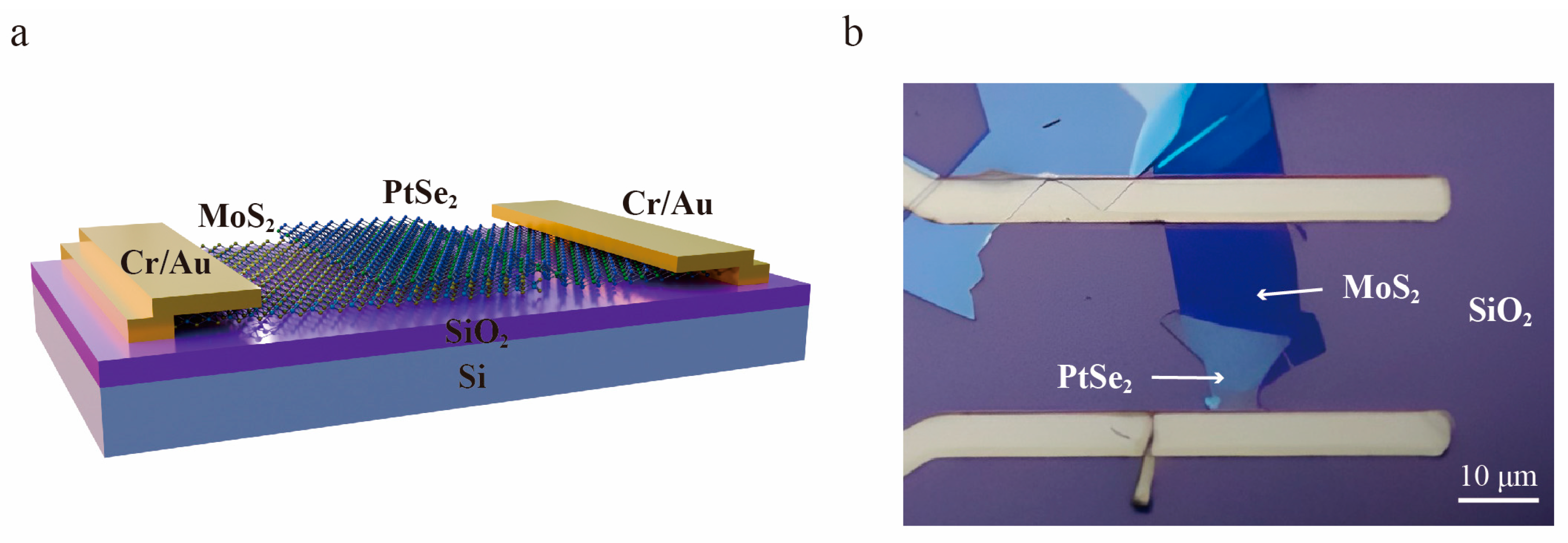
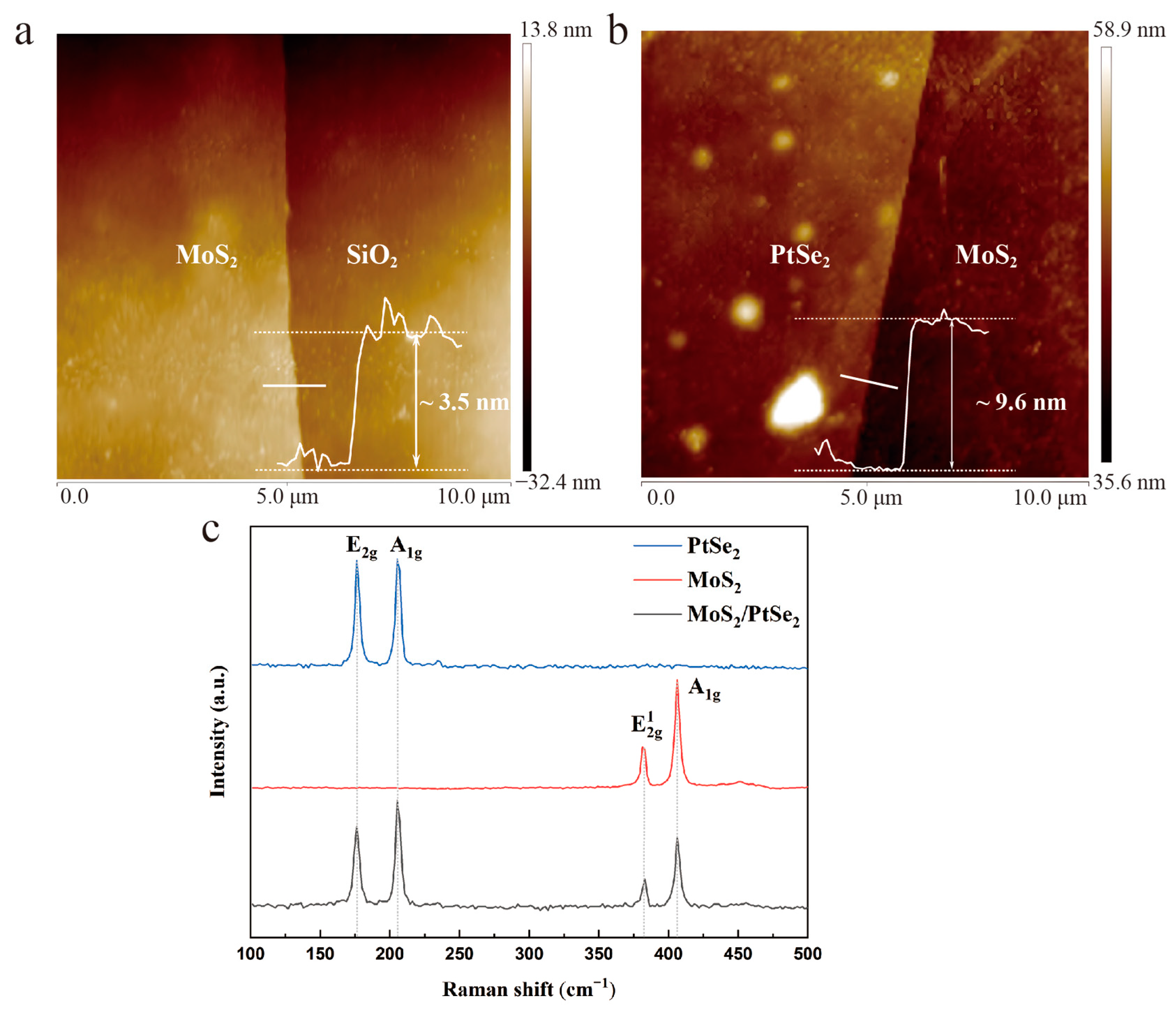
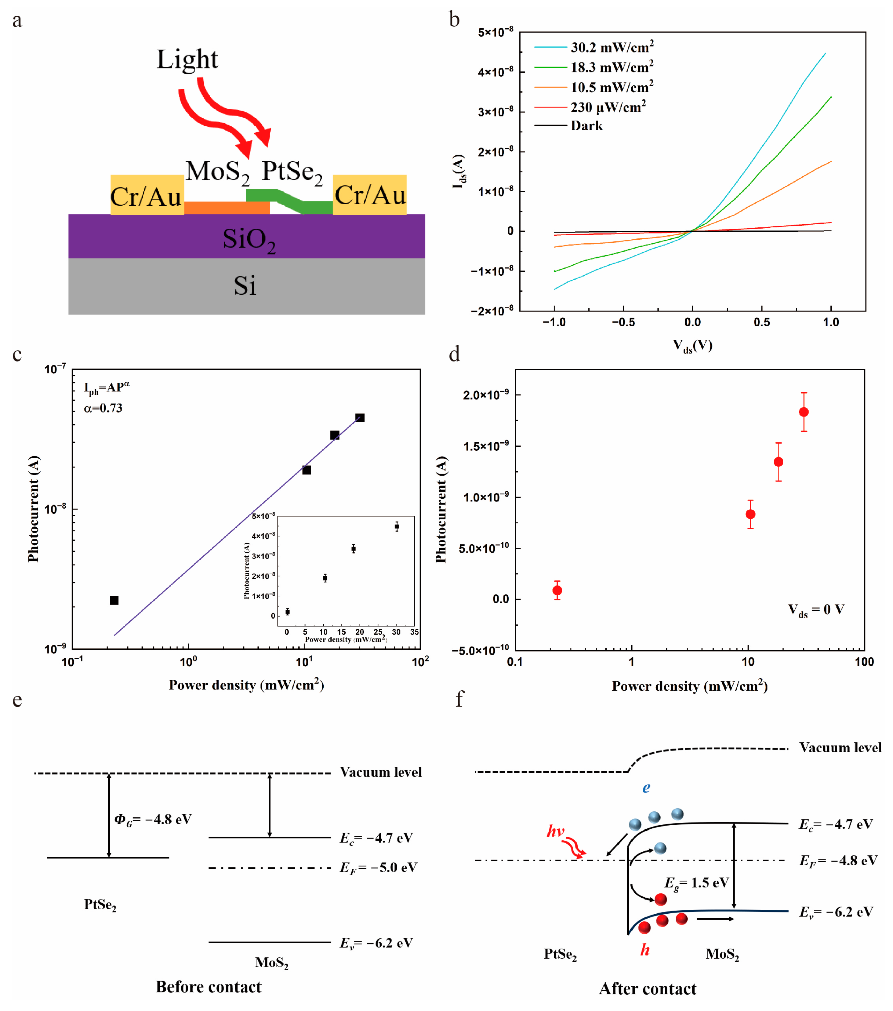
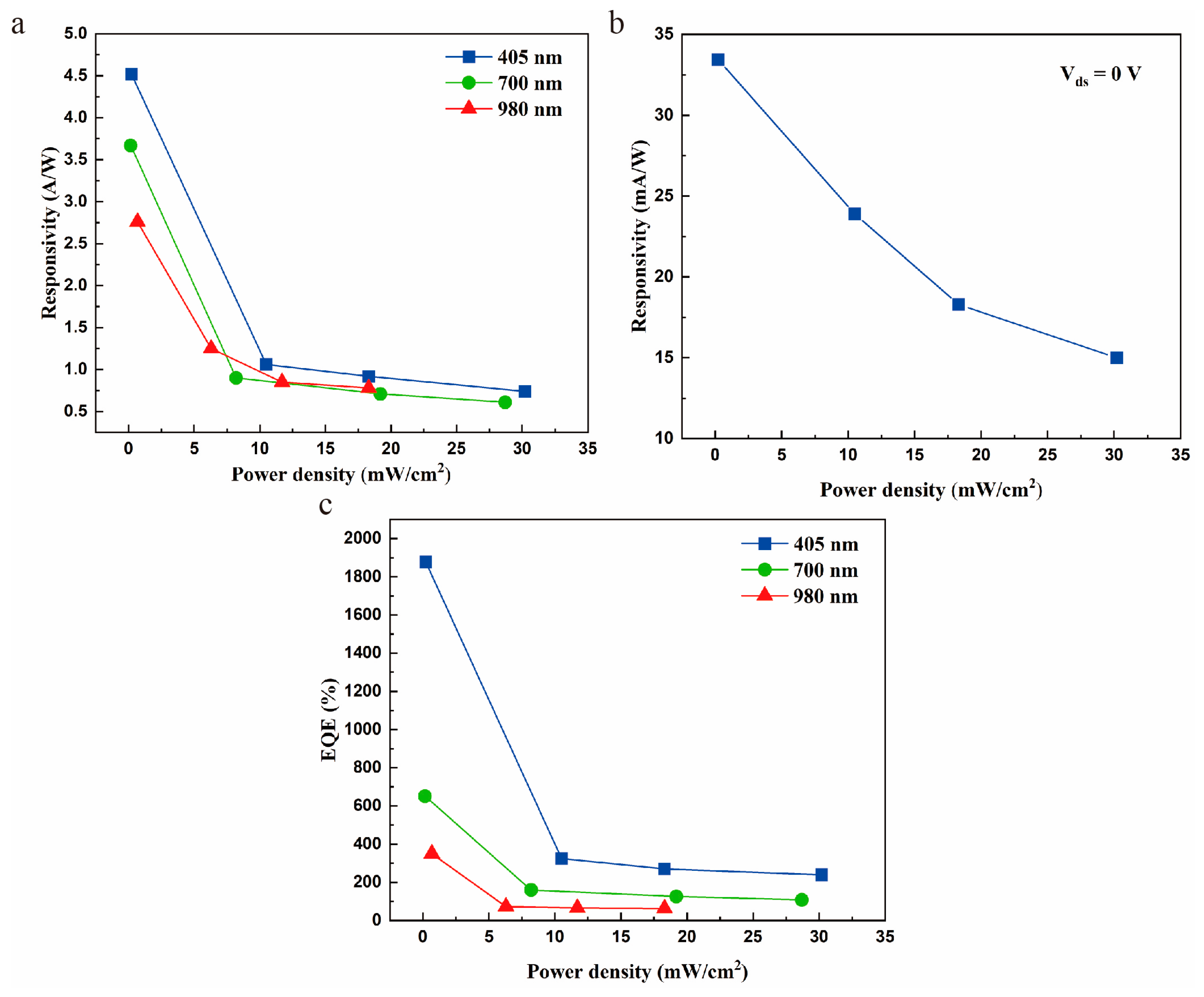
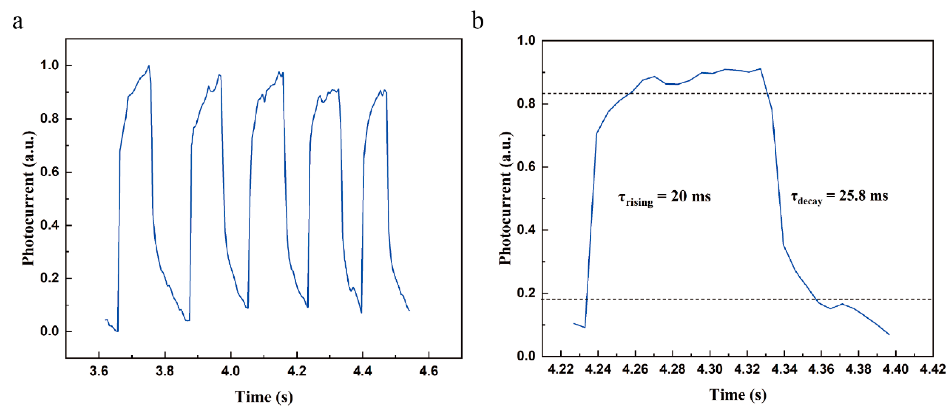
2. Results and Discussion

Here, PtSe2/MoS2 heterostructure was fabricated by mechanical exfoliation and dry transfer method. Few-layer MoS2 and PtSe2 were subsequently transferred on the SiO2 (300 nm)/Si substrate to form an optimal heterostructure. The detailed process of heterostructure preparation is illustrated in the Materials and Methods section. Figure 1a,b depicts the schematic diagram of the photodetector based on PtSe2/MoS2 heterostructure and an optical image of the device, respectively. The dark blue portion of the heterostructure is 2D MoS2, while the light gray portion belongs to 2D PtSe2. In addition, The Au/Cr (80 nm/15 nm) electrodes of the device were prepared by standard photolithography and thermal evaporation. Herein, given the weak adhesion of the Au, Cr layer was used to improve the adhesion between electrodes and substrate. In addition, the channel width of the heterostructure device is 50 μm. Conversely, the channel length is 20 μm. As depicted in Figure 1b, the PtSe2 layer was superimposed on the MoS2 layer, which allows the overlapping area to be determined based on the contrast of colors. In addition, the area of the overlapping region can be estimated by calculating the area of a triangle. For an estimate based on the scale, the overlapping area is approximately 50 μm2. Owing to the 2D PtSe2 having wider absorption spectra than that of few-layer MoS2, the PtSe2 layer was transferred to the top of the heterostructure.
To precisely evaluate the thickness and morphology of PtSe2/MoS2 heterostructure, it was measured by AFM. Herein, the thickness of MoS2 is estimated to be 3.5 nm, and PtSe2 is approximately 9.6 nm, respectively (Figure 2a,b). Monolayer MoS2 and PtSe2 have thicknesses of roughly 0.65 nm and 0.88 nm, respectively [19,25]. Thus, the number of layers of MoS2 is approximately five, while the number of PtSe2 layers is approximately 11. Furthermore, the Raman spectra of separated PtSe2, separated MoS2, and PtSe2/MoS2 heterostructure were measured. The wavelength of the used laser is 532 nm. As depicted in Figure 2c, in PtSe2 region, the two characteristic peaks of the Raman spectrum of E2g and A1g were located at 176.3 cm−1 and 205.4 cm−1, respectively, which belong to the Eg in-plane vibration mode and A1g out-of-plane vibration mode of the Se atom, respectively. The peak intensity of E2g and A1g is similar. This phenomenon proves that the number of PtSe2 layer is approximately 10 [26]. Moreover, for 2D MoS2, the in-plane vibration mode E 2 g 1 and out-of-plane vibration A1g mode were located at 381.5 cm−1 and 406.1 cm−1, respectively. The measured energy difference of MoS2 can also be used to estimate the layer number is approximately five, which is consistent with the AFM results [25]. Both results of PtSe2 and MoS2 are consistent with the previous reports [27,28], indicating that few-layer PtSe2 and MoS2 nanosheets were mechanical exfoliated. In addition, these peaks all appear in the Raman spectra in the overlapping region of the heterostructure without obvious peak shift, confirming the formation of a good-quality van der Waals heterostructure after the fabrication process. The intensity of the measured Raman characteristic peak in the heterostructure region decreases compared with that of a single material, which is ascribed to the interlayer coupling within the overlapping area of different materials [29].
To assess the optoelectronic properties of the PtSe2/MoS2 device, further characterization was implemented under the illumination of different wavelengths (405 nm, 700 nm and 980 nm). Without specific description, all the experiments were conducted on the photodetector portrayed in Figure 1b. Herein, the measured current of the photodetector shows a strong dependence on the power density. Figure 3b illustrates the Ids-Vds characteristic of PtSe2/MoS2 photodetector under conditions of darkness and 405 nm light illumination with different power densities (230 μW/cm2–30.2 mW/cm2). (The Ids-Vds characteristic under illumination of 700 nm and 980 nm can be found in Figure S1). A nonlinear Ids-Vds characteristic was observed which ascribed to the good contact of the interface of the heterostructure. The Ids under forward bias is much larger than that under reverse bias. Under the illumination of different power densities (230 μW/cm2, 18.3 mW/cm2, 10.5 mW/cm2 and 30.2 mW/cm2) of the illumination, Ids of the heterostructure reaches the value of 4.48 × 10⁻⁸ A, 3.37 × 10⁻⁸ A, 1.75 × 10⁻⁸ A and 2.23 × 10⁻⁹ A, respectively, with applied external bias of 1 V. In addition, the dark current of the device is as low as 1.7 × 10⁻¹⁰ A (Vds = 1 V), which is approximately four orders of magnitude smaller than that of PtSe2-based photodetector [18]. The reason for the low dark current is that the barrier at the interface of heterostructure limits the carrier drift. As the power density of illumination increases, the generated carriers increase significantly, and the photocurrent increases correspondingly. This phenomenon demonstrates that the measured photocurrent has a strong dependence on light intensity. The measured photocurrent also shows a similar trend under different power densities of 700 nm and 980 nm illumination. Based on the recorded experimental data, to systematically study the photoresponse of PtSe2/MoS2 photodetector, the net photocurrent (Iph = IdsIdark) was extracted at Vds = 1 V, which is dependent on the illumination power density, where Idark stands for the dark current of the device. As depicted in Figure 3c, Iph exhibits a sublinear increasing trend which able to be illustrated by the power law formula of:
I = A P α
where A is a constant, P represents the incident power density and α represents the power law index, which is closely related to the quality of the photodetector. When α = 0 and the photogating effect determines the generation of photocurrent [30]. Conversely, when α = 1, the photoconductivity effect becomes the main mechanism of photocurrent generation. The value of α is usually used to analyze the mechanism of photocurrent generation. Herein, α can be extracted as 0.73, 0.68, and 0.66 for 405 nm, 700 nm and 980 nm, respectively (Figure S2). Furthermore, the value of α deviating from 1 means the loss of photogenerated carriers. Therefore, such a power law behavior indicates there are some trap states exist at the interface of PtSe2 and MoS2. Therefore, the photocurrent generation of the device was determined by these two effects. With the increasing power density, more photogenerated carriers will fill in the trap states, which can effectively enhance the possibility of photocarrier recombination and decrease the lifetime of carriers (τ). The saturation of the photocurrent leads to the lower value of the power law index α because of this. An analogous α variation trend was previously observed in other photodetectors based on 2D heterostructures [31].
As a new type of the state-of-art photodetection device, self-powered photodetectors have begun to receive more and more attention [32]. The ability to realize photodetection without external power supplies increases the possibility of applications in complex environments. Given this, we demonstrate that the PtSe2/MoS2 heterostructure can operate in self-driven mode. The photoresponse characteristic of the self-driven PtSe2/MoS2 heterostructure was also investigated. Under zero bias, Figure 3d plots the Ids-Vds under 405 nm light irradiation ranging from 230 μW/cm2 to 30.2 mW/cm2. When the power density increases, photocurrent increased gradually, indicating the PtSe2/MoS2 device able to operate in self-driven mode [33]. When the power density is 230 μW/cm2, the photocurrent can reach 8.87 × 10⁻¹¹ A. The ability of the PtSe2/MoS2 heterostructure to detect weak signals without external bias highlighting the application potential in optical communication. It is also worth noting that the device was tested multiple times under the same measurement conditions. As shown in Figure 3d, the calculated error bar clearly indicates that the detector can work stably.
To better understand the operating mechanism of PtSe2/MoS2 photodetector, the band diagrams of the two different materials before and after contact were drawn based on their characteristics [27,34]. As shown in Figure 3e, the 11-layer PtSe2 can be regarded as a semimetal [31]. The Fermi level of the multi-layer PtSe2 is approximately 0.2 eV higher than that of MoS2 [27,34]. Therefore, when multi-layer PtSe2 is in contact with few-layer MoS2, electrons flow from PtSe2 to MoS2, and holes flow toward opposite directions (Figure 3f). Eventually, a strong built-in electric field is formed at the interface from PtSe2 to MoS2 when the heterostructure reaches equilibrium, resulting in the obvious band-bending. This formed barrier can efficiently suppress the dark current, which is beneficial to obtaining a higher net photocurrent. When the incident light irradiates the surface of the material, electron-hole pairs are generated and separated by the built-in potential then collected by electrodes to increase photocurrent significantly. Furthermore, the external electric field can effectively promote the separation of carriers in the reverse biased photodetector, which increases the photocurrent significantly. Therefore, the net photocurrent of the PtSe2/MoS2 heterostructure is much larger than the dark current, which gives it a decent photodetection capability.
Some important figure-of-merits (FOMs) of the PtSe2/MoS2 photodetector can be calculated using the measured Iph. Photoresponsivity (Rλ) plays a significant role in determine the performance of photodetectors and the expression is:
R = I p h / P S
where Iph is the net photocurrent, P is the power density of the illumination with different wavelengths, and S denotes the effective responsive region. Photoresponsivity precisely reflects the merits of the photoelectric conversion efficiency of the photodetection device. Therefore, it is essential to study the responsivity of the device. Based on Equation (2), the responsivity of PtSe2/MoS2 heterostructure was calculated to be 4.52 A/W for 405 nm illumination with power density of 230 μW/cm2, which is approximately hundreds of times higher than that of MoS2/CdTe heterostructure based photodetector (10 mA/W, 405 nm) [35]. Under the same eternal bias (Vds = 1 V), the responsivity of the device at 700 nm was approximately 3.67 A/W. Moreover, when the detection wavelength is up to NIR (980 nm), the responsivity of the device is still able to reach 2.76 A/W. This value of the heterostructure is significantly higher than that of a device based on PtSe2/CdTe heterostructure [36]. These results demonstrate the PtSe2/MoS2 device is highly sensitive to visible and NIR illumination. The main reason for the high responsivity is the built-in potential at the interface of PtSe2 and MoS2 can effectively promote carrier separation. Moreover, the high carrier mobility of PtSe2 is also valuable for decent responsivity. In addition, as depicted in Figure 4a, the responsivity of the PtSe2/MoS2 photodetector decreases with increasing incident power density. This finding indicates that the trap states capture the photogenerated carriers under low power intensity, which leads to a reduction of carrier recombination possibility [37]. Meanwhile, it also demonstrates that lower proportion of photogenerated carriers are collected at high light power intensity [38]. The generated carriers may screen the internal field could be another reason for the relationship of responsivity on light intensity [39].
Conversely, detectivity (D*) is an important FOM to evaluate the sensitivity of photodetectors. The value of detectivity can be calculated by equation:
D * = R λ S 1 2 ( 2 e I d a r k ) 1 2
where Rλ is the photoresponsivity, S represents the effective portion of the heterostructure, e represents the electronic charge and Idark is the dark current, respectively. The detectivity of PtSe2/MoS2 heterostructure was as high as 9.24 × 10¹¹ Jones at 405 nm. Furthermore, the detectivity at 700 nm and 980 nm can achieve up to 7.5 × 10¹¹ Jones and 5.63 × 10¹¹ Jones, respectively. The detectivity of the device is outperformed than that of single MoS2-based photodetector [40]. For the purpose of accurately calculating the detectivity of the photodetector, the noise of the device should be systemically examined and studied under different frequencies [41]. As a future work, further measurements will be comprehensively carried out to characterize the noise current of the device. The noise-related detectivity under different frequencies will be accurately measured as well.
In addition, external quantum efficiency (EQE) is regarded as a critical FOM of the photodetector, which is the ratio between the generated electron-hole pair per second and the number of incident photons per second. EQE characterizes the efficiency of a photodetector in converting photons into electrons. In addition, EQE can be obtained by equation:
E Q E = R h c / e λ
where h is the Planck constant and c is the speed of light. As depicted in Figure 4c, EQE exhibits a similar varying trend with the power density as the responsivity, reaching the highest value of 1880%, 641% and 349% for 405 nm, 700nm and 980 nm, respectively. The high EQE is much greater than the photodetector based on WSe2/SnSe2 heterostructure [42]. Here, EQE is higher than 100% indicating a large gain in the photodetector, which may attributed to the photogenerated carriers recirculated multiple times before reaching the electrodes [43].
In addition, we also calculated and analyzed the critical FOMs of the PtSe2/MoS2 photodetector which operates in self-driven mode. The responsivity of the self-driven PtSe2/MoS2 device is up to 33.4 mA/W at 405 nm (Figure 4b), which outperforms than that of the MoS2/WS2 heterostructure based self-driven photodetector [44]. The characteristic of working without external bias gives the heterostructure fine application prospects in the field of highly sensitive detections. Furthermore, under 405 nm illumination, the EQE of the self-driven PtSe2/MoS2 heterostructure is still 139%.
Response time is another fundamental FOM which determines the maximum operating frequency of a photodetector. In previous studies, the response time of 2D heterostructure-based photodetectors is able to outperform than that of a single 2D material-based device [45]. The response of PtSe2/MoS2 photodetector was measured under the illumination of 405 nm wavelength with 30.2 mW/cm2 power density, which was switched between on and off states on a regular basis. As shown in Figure 5a, the time-dependent photoresponse maintains excellent stability and reliability after several switching cycles. Generally, rise time (τrising) and decay time (τdecay) can be defined by the amount of changing time from 10%/90% to 90%/10% of net photocurrent. Herein, a photocurrent within a switching cycle is selected for analysis (Figure 5b). The measured τrising and τdecay are 20 ms and 25.8 ms, respectively. The performance is comparable to those photodetectors based on mechanical exfoliated and transferred van der Waals heterostructure [46,47]. The steep edge of both the rise and decay time clearly indicates that the photogenerated carriers are able to separate promptly. The response time is limited by the phenomenon that carriers are trapped during the transport from the heterostructure to the metal contacts [47]. The response time can be improved by designing suitable patterned electrodes to facilitate the collection of photogenerated carriers. In addition, fabricating heterostructure with clean interface or reducing electrode spacing are also optimal methods to shorten response time [40]. All these results indicate that the PtSe2/MoS2 heterostructure is important for the development of state-of-art image processing and optical communications.

3. Materials and Methods

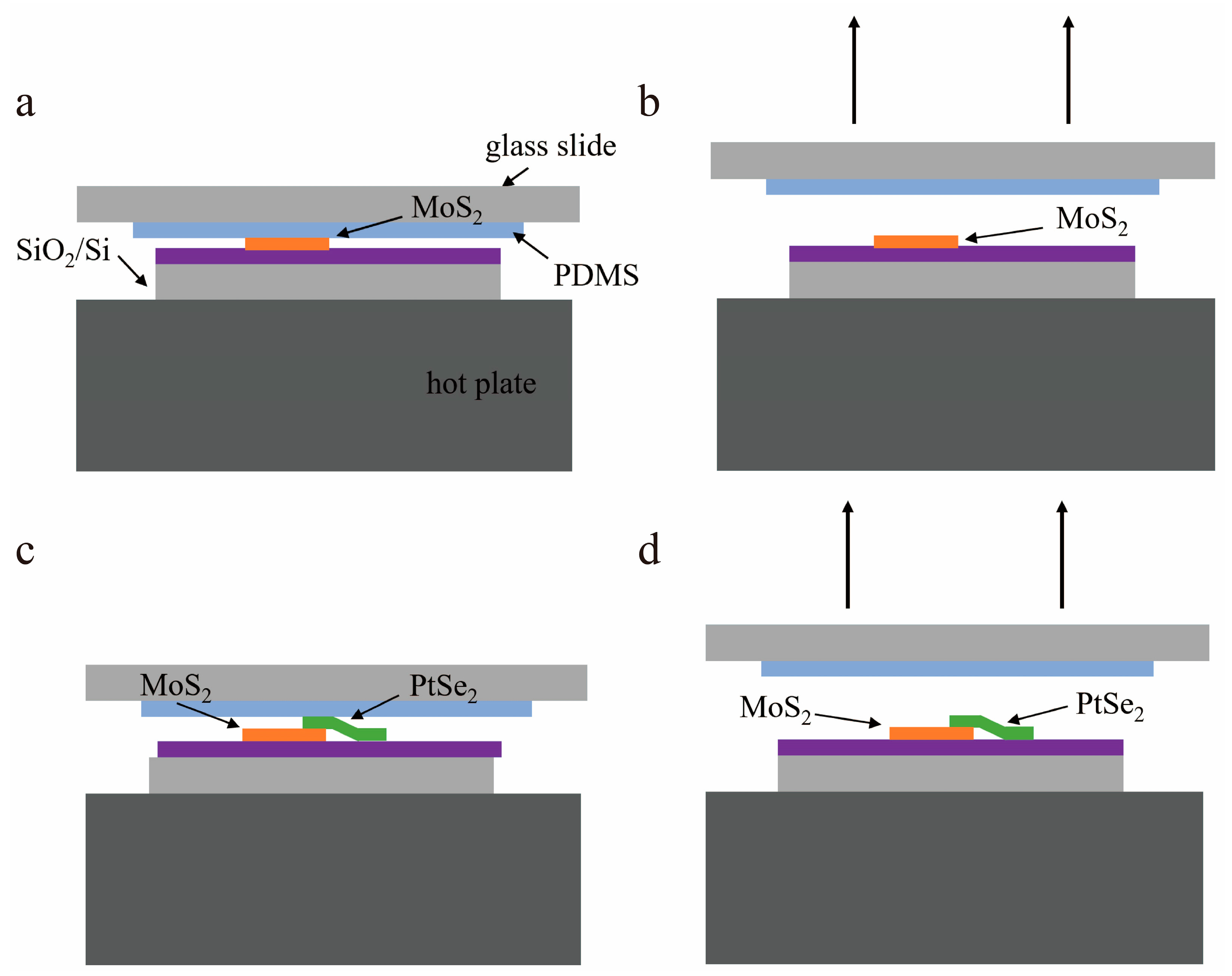
3.1. Fabrication of PtSe2/MoS2 Heterostructure Photodetector

Figure 6 illustrates a detailed fabrication process of PtSe2/MoS2 heterostructure. Bulk PtSe2 and MoS2 were purchased from Nanjing MKNANO Tech. Co. Ltd. (Nanjing, China). The 2D PtSe2/MoS2 heterostructure was prepared by dry transfer with the assistance of polydimethylsiloxane (PDMS). First, the few layer 2D MoS2 was prepared by mechanical exfoliation. The tape with MoS2 was then tightly pasted with the PDMS film, pressed the tape with gentle pressure, and the MoS2 was transferred to PDMS completely. As shown in Figure 6a,b, the PDMS with 2D MoS2 stamped onto SiO2 (300 nm)/Si substrate and heated up to 80 °C for 5 min, then 2D MoS2 can be completely transferred to the substrate. After that, repeating a similar process (Figure 6c,d), the PtSe2 layer was stacked on 2D MoS2 when the substrate was heated up to 100 degrees. With the assistance of an optical microscope, the overlapping region of the PtSe2/MoS2 heterostructure can be precisely controlled. After spin-coating the S1813 photoresist on the substrate at the speed of 6000 rpm for 30 s, it was baked at 100 degrees for 1 min. Then, the designed electrodes were patterned on the PtSe2/MoS2 heterostructure by photolithography. The Cr (15 nm)/Au (80 nm) was deposited on the heterostructure by thermal evaporation, then followed by standard lift-off process to remove the undesired photoresist.

3.2. Characterization of PtSe2/MoS2 Heterostructure

The morphologies structure of the PtSe2/MoS2 heterostructure was characterized by an optical microscope whose model is WITec, alpha 300R (Oxford Instruments, Abingdon, UK). The Raman spectra were studied by using a Raman spectrometer (model: HORIBA JOBIN YVON, HR800, Horiba, Kyoto, Japan), with a 532 nm laser source. Bruker Dimension Icon AFM (Bruker, Billerica, MA, USA) was used to study the thickness of 2D MoS2 and 2D PtSe2. A micromanipulator probe station SM-4 with a Keithley 2450 (Tektronix, Hongkong, China) source meter was used to investigate the optoelectronic properties of PtSe2/MoS2 photodetector. The light source used in experiments were light emitting diodes at 405 nm, 700 nm and 980 nm. Every measurement was carried out at room temperature in ambient conditions.

4. Conclusions

In summary, a high-performance photodetector based on PtSe2/MoS2 heterostructure has been designed and successfully fabricated. The characteristics of the photodetector were fully investigated. The device has demonstrated a wide range of photodetection from visible (405 nm) to NIR (980 nm). Furthermore, the photodetector exhibits many excellent FOMs including high responsivity (4.52 A/W for 405 nm, 3.67 A/W for 700 nm, 2.76 A/W for 980 nm); high EQE (1880% for 405 nm, 641% for 700nm and 349% for 980 nm); and fast response time (20 ms/25.8 ms), which makes it promising for application in high-performance optoelectronics. In addition, the detector has been found able to work in self-driven mode. Under 405 nm illumination, the responsivity and EQE of the photodetector operating in the self-driven mode can reach 33.4 mA/W and 139%, respectively. Such properties of PtSe2/MoS2 photodetector demonstrated in this work pave a new way for the development of high-performance photodetection applications. In future work, the detecting range of the heterostructure device ought to be further expanded to meet the requirements of modern science and technology for broadband detection. Additionally, the large-scale synthesis of PtSe2/MoS2 heterostructure also needs to be investigated. Furthermore, in order to achieve better application in practice, arrayed photodetectors and imaging devices will be developed as well.

Supplementary Materials

The following supporting information can be downloaded at: https://www.mdpi.com/article/10.3390/molecules29112553/s1, Figure S1: Ids-Vds curve of PtSe2/MoS2 photodetector under 700 nm and 980 nm irradiation; Figure S2: Photocurrent as a function of power density under 700 nm and 980 nm irradiation.

Author Contributions

Conceptualization, H.L. and Z.Y.; methodology, H.L. and Z.Y.; validation, H.L. and Z.Y.; formal analysis, H.L. and Z.Y.; investigation, H.L.; writing—original draft preparation, H.L.; writing—review and editing, Z.Y.; supervision, Z.Y; funding acquisition, Z.Y. All authors have read and agreed to the published version of the manuscript.

Funding

The research was funded by the National Natural Science Foundation of China, grant number 62105236.

Institutional Review Board Statement

Not applicable.

Informed Consent Statement

Not applicable.

Data Availability Statement

Data are contained within the article and Supplementary Materials.

Conflicts of Interest

The authors declare no conflicts of interest.

References

  1. Konstantatos, G.; Sargent, E.H. Nanostructured Materials for Photon Detection. Nat. Nanotechnol. 2010, 5, 391–400. [Google Scholar] [CrossRef] [PubMed]
  2. Wu, Y.L.; Fukuda, K.; Yokota, T.; Someya, T. A Highly Responsive Organic Image Sensor Based on a Two-Terminal Organic Photodetector with Photomultiplication. Adv. Mater. 2019, 31, 1903687. [Google Scholar] [CrossRef] [PubMed]
  3. Rogalski, A. Infrared Detectors: Status and Trends. Prog. Quantum Electron. 2003, 27, 59–210. [Google Scholar] [CrossRef]
  4. Gui, T.; Xia, X.; Wei, B.; Zhang, J.; Zhang, K.; Li, Y.; Chen, W.; Yu, W.; Cui, N.; Mu, H. In-Situ Fabrication of PtSe2/MoS2 Van der Waals Heterojunction for Self-Powered and Broadband Photodetector. Mater. Des. 2024, 238, 112722. [Google Scholar] [CrossRef]
  5. Yang, Z.B.; Guo, J.X.; Li, H.R.; Du, X.N.; Zhao, Y.N.; Chen, H.S.; Chen, W.W.; Zhang, Y. Large-Scale Synthesis of Two-Dimensional Indium Telluride Films for Broadband Photodetectors. Mater. Des. 2023, 233, 112218. [Google Scholar] [CrossRef]
  6. Manzeli, S.; Ovchinnikov, D.; Pasquier, D.; Yazyev, O.V.; Kis, A. 2D Transition Metal Dichalcogenides. Nat. Rev. Mater. 2017, 2, 17033. [Google Scholar] [CrossRef]
  7. Bullock, J.; Amani, M.; Cho, J.; Chen, Y.-Z.; Ahn, G.H.; Adinolfi, V.; Shrestha, V.R.; Gao, Y.; Crozier, K.B.; Chueh, Y.-L. Polarization-Resolved Black Phosphorus/Molybdenum Disulfide Mid-Wave Infrared Photodiodes with High Detectivity at Room Temperature. Nat. Photonics 2018, 12, 601–607. [Google Scholar] [CrossRef]
  8. Yang, Z.; Hao, J.; Yuan, S.; Lin, S.; Yau, H.M.; Dai, J.; Lau, S.P. Field-Effect Transistors Based on Amorphous Black Phosphorus Ultrathin Films by Pulsed Laser Deposition. Adv. Mater. 2015, 27, 3748–3754. [Google Scholar] [CrossRef]
  9. Li, H.; Yang, Z. Recent Progress in Synthesis and Photonic Applications of Two-Dimensional Bismuthene. Appl. Sci. 2023, 13, 6885. [Google Scholar] [CrossRef]
  10. Chhowalla, M.; Liu, Z.; Zhang, H. Two-Dimensional Transition Metal Dichalcogenide (TMD) Nanosheets. Chem. Soc. Rev. 2015, 44, 2584–2586. [Google Scholar] [CrossRef]
  11. Mak, K.F.; Shan, J. Photonics and Optoelectronics of 2D Semiconductor Transition Metal Dichalcogenides. Nat. Photonics 2016, 10, 216–226. [Google Scholar] [CrossRef]
  12. Wang, B.; Yuan, J.; Che, M.; Liu, M.; Zou, Y.; An, J.; Tan, F.; Shi, Y.; Zhang, N.; Qi, L. High-Performance Broadband Photodetector Based on PtSe2/MoS2 Heterojunction from Visible to Near-Infrared Region. Sci. China Inf. Sci. 2024, 67, 132401. [Google Scholar] [CrossRef]
  13. Venkata Subbaiah, Y.; Saji, K.; Tiwari, A. Atomically Thin MoS2: A Versatile Nongraphene 2D Material. Adv. Funct. Mater. 2016, 26, 2046–2069. [Google Scholar] [CrossRef]
  14. Xie, Y.; Zhang, B.; Wang, S.; Wang, D.; Wang, A.; Wang, Z.; Yu, H.; Zhang, H.; Chen, Y.; Zhao, M. Ultrabroadband MoS2 Photodetector with Spectral Response From 445 to 2717 nm. Adv. Mater. 2017, 29, 1605972. [Google Scholar] [CrossRef] [PubMed]
  15. Wang, G.; Wang, Z.; McEvoy, N.; Fan, P.; Blau, W.J. Layered PtSe2 for Sensing, Photonic, and (Opto-) Electronic Applications. Adv. Mater. 2021, 33, 2004070. [Google Scholar] [CrossRef]
  16. Xu, H.; Zhang, H.; Liu, Y.; Zhang, S.; Sun, Y.; Guo, Z.; Sheng, Y.; Wang, X.; Luo, C.; Wu, X. Controlled Doping of Wafer-Scale PtSe2 Films for Device Application. Adv. Funct. Mater. 2019, 29, 1805614. [Google Scholar] [CrossRef]
  17. Ye, P.; Xiao, H.; Zhu, Q.; Kong, Y.; Tang, Y.; Xu, M. Si-CMOS-Compatible 2D PtSe2-Based Self-Driven Photodetector with Ultrahigh Responsivity and Specific Detectivity. Sci. China. Mater. 2023, 66, 193–201. [Google Scholar] [CrossRef]
  18. Zhao, Y.; Qiao, J.; Yu, Z.; Yu, P.; Xu, K.; Lau, S.P.; Zhou, W.; Liu, Z.; Wang, X.; Ji, W. High-Electron-Mobility and Air-Stable 2D Layered PtSe2 FETs. Adv. Mater. 2017, 29, 1604230. [Google Scholar] [CrossRef]
  19. Liu, J.; Xia, F.; Xiao, D.; Garcia de Abajo, F.J.; Sun, D. Semimetals for High-Performance Photodetection. Nat. Mater. 2020, 19, 830–837. [Google Scholar] [CrossRef]
  20. Rao, G.F.; Wang, X.P.; Wang, Y.; Wangyang, P.H.; Yan, C.Y.; Chu, J.W.; Xue, L.X.; Gong, C.H.; Huang, J.W.; Xiong, J.; et al. Two-Dimensional Heterostructure Promoted Infrared Photodetection Devices. Infomat 2019, 1, 272–288. [Google Scholar] [CrossRef]
  21. Xu, H.; Han, X.; Dai, X.; Liu, W.; Wu, J.; Zhu, J.; Kim, D.; Zou, G.; Sablon, K.A.; Sergeev, A. High Detectivity and Transparent Few-Layer MoS2/Glassy-Graphene Heterostructure Photodetectors. Adv. Mater. 2018, 30, 1706561. [Google Scholar] [CrossRef]
  22. Tao, L.; Chen, Z.; Li, X.; Yan, K.; Xu, J.-B. Hybrid Graphene Tunneling Photoconductor with Interface Engineering Towards Fast Photoresponse and High Responsivity. Npj 2D Mater. Appl. 2017, 1, 19. [Google Scholar] [CrossRef]
  23. Chang, K.E.; Kim, C.; Yoo, T.J.; Kwon, M.G.; Heo, S.; Kim, S.Y.; Hyun, Y.; Yoo, J.I.; Ko, H.C.; Lee, B.H. High-Responsivity Near-Infrared Photodetector Using Gate-Modulated Graphene/Germanium Schottky Junction. Adv. Electron. Mater. 2019, 5, 1800957. [Google Scholar] [CrossRef]
  24. Wang, G.C.; Sun, Y.; Yang, Z.; Lu, W.X.; Chen, S.; Zhang, X.H.; Ma, H.Q.; Sun, T.Y.; Huo, P.P.; Cui, X.Y.; et al. Near-Ideal Schottky Junction Photodetectors Based on Semimetal-Semiconductor Van der Waals Heterostructures. Adv. Funct. Mater. 2024. [Google Scholar] [CrossRef]
  25. Sam, R.T.; Umakoshi, T.; Verma, P. Probing Stacking Configurations In a Few Layered MoS2 by Low Frequency Raman Spectroscopy. Sci. Rep. 2020, 10, 21227. [Google Scholar] [CrossRef]
  26. Tharrault, M.; Desgué, E.; Carisetti, D.; Plaçais, B.; Voisin, C.; Legagneux, P.; Baudin, E. Raman Spectroscopy of Monolayer to Bulk PtSe2 Exfoliated Crystals. 2D Mater. 2024, 11, 025011. [Google Scholar] [CrossRef]
  27. Su, W.-J.; Chang, H.-C.; Shih, Y.-T.; Wang, Y.-P.; Hsu, H.-P.; Huang, Y.-S.; Lee, K.-Y. Two Dimensional MoS2/Graphene PN Heterojunction Diode: Fabrication and Electronic Characteristics. J. Alloys Compd. 2016, 671, 276–282. [Google Scholar] [CrossRef]
  28. Ji, J.; Zhou, Y.; Zhou, B.; Desgué, E.; Legagneux, P.; Jepsen, P.U.; Bøggild, P. Probing Carrier Dynamics in Large-Scale MBE-Grown PtSe2 Films by Terahertz Spectroscopy. ACS Appl. Mater. Interfaces 2023, 15, 51319–51329. [Google Scholar] [CrossRef]
  29. Tongay, S.; Fan, W.; Kang, J.; Park, J.; Koldemir, U.; Suh, J.; Narang, D.S.; Liu, K.; Ji, J.; Li, J. Tuning Interlayer Coupling in Large-Area Heterostructures with CVD-Grown MoS2 and WS2 Monolayers. Nano Lett. 2014, 14, 3185–3190. [Google Scholar] [CrossRef]
  30. Wang, W.; Meng, Y.; Wang, W.; Zhang, Z.; Xie, P.; Lai, Z.; Bu, X.; Li, Y.; Liu, C.; Yang, Z. Highly Efficient Full Van der Waals 1D P-Te/2D N-Bi2O2Se Heterodiodes with Nanoscale Ultra-Photosensitive Channels. Adv. Funct. Mater. 2022, 32, 2203003. [Google Scholar] [CrossRef]
  31. Song, Y.; Li, M.; Chen, J.; Du, Y.; Qin, Q.; Du, Z.; Zou, F.; Ma, X.; Li, L.; Li, G. High-Performance Photodetector Based on the ReSe2/PtSe2 Van der Waals Heterojunction. ACS Appl. Electron. Mater. 2023, 5, 2748–2757. [Google Scholar] [CrossRef]
  32. Qiao, H.; Huang, Z.; Ren, X.; Liu, S.; Zhang, Y.; Qi, X.; Zhang, H. Self-Powered Photodetectors Based on 2D Materials. Adv. Opt. Mater. 2020, 8, 1900765. [Google Scholar] [CrossRef]
  33. Sun, H.; Lei, T.; Tian, W.; Cao, F.; Xiong, J.; Li, L. Self-Powered, Flexible, and Solution-Processable Perovskite Photodetector Based on Low-Cost Carbon Cloth. Small 2017, 13, 1701042. [Google Scholar] [CrossRef]
  34. Zeng, L.H.; Lin, S.H.; Li, Z.J.; Zhang, Z.X.; Zhang, T.F.; Xie, C.; Mak, C.H.; Chai, Y.; Lau, S.P.; Luo, L.B. Fast, Self-Driven, Air-Stable, and Broadband Photodetector Based on Vertically Aligned PtSe2/GaAs heterojunction. Adv. Funct. Mater. 2018, 28, 1705970. [Google Scholar] [CrossRef]
  35. Wang, Y.; Huang, X.; Wu, D.; Zhuo, R.; Wu, E.; Jia, C.; Shi, Z.; Xu, T.; Tian, Y.; Li, X. A Room-Temperature Near-Infrared Photodetector Based on a MoS2/CdTe P–N Heterojunction with a Broadband Response up to 1700 nm. J. Mater. Chem. C 2018, 6, 4861–4865. [Google Scholar] [CrossRef]
  36. Wu, D.; Wang, Y.; Zeng, L.; Jia, C.; Wu, E.; Xu, T.; Shi, Z.; Tian, Y.; Li, X.; Tsang, Y.H. Design of 2D layered PtSe2 Heterojunction for the High-Performance, Room-Temperature, Broadband, Infrared Photodetector. ACS Photonics 2018, 5, 3820–3827. [Google Scholar] [CrossRef]
  37. Kong, W.-Y.; Wu, G.-A.; Wang, K.-Y.; Zhang, T.-F.; Zou, Y.-F.; Wang, D.-D.; Luo, L.-B. Graphene-β-Ga2O3 heterojunction for highly sensitive deep UV photodetector application. Adv. Mater. 2016, 28, 10725–10731. [Google Scholar] [CrossRef]
  38. Zhang, K.; Fang, X.; Wang, Y.; Wan, Y.; Song, Q.; Zhai, W.; Li, Y.; Ran, G.; Ye, Y.; Dai, L. Ultrasensitive Near-Infrared Photodetectors Based on a Graphene–MoTe2–Graphene Vertical Van der Waals Heterostructure. ACS Appl. Mater. Interfaces 2017, 9, 5392–5398. [Google Scholar] [CrossRef]
  39. Zhang, X.; Li, J.; Ma, Z.; Zhang, J.; Leng, B.; Liu, B. Design and Integration of a Layered MoS2/GaN Van Der Waals Heterostructure For Wide Spectral Detection and Enhanced Photoresponse. ACS Appl. Mater. Interfaces 2020, 12, 47721–47728. [Google Scholar] [CrossRef]
  40. Tsai, D.-S.; Liu, K.-K.; Lien, D.-H.; Tsai, M.-L.; Kang, C.-F.; Lin, C.-A.; Li, L.-J.; He, J.-H. Few-Layer MoS2 With High Broadband Photogain and Fast Optical Switching for Use in Harsh environments. ACS Nano 2013, 7, 3905–3911. [Google Scholar] [CrossRef]
  41. Wang, F.; Zhang, T.; Xie, R.; Wang, Z.; Hu, W. How to Characterize Figures of Merit of Two-Dimensional Photodetectors. Nat. Commun. 2023, 14, 2224. [Google Scholar] [CrossRef]
  42. Lee, J.; Duong, N.T.; Bang, S.; Park, C.; Nguyen, D.A.; Jeon, H.; Jang, J.; Oh, H.M.; Jeong, M.S. Modulation of Junction Modes in SnSe2/MoTe2 Broken-Gap Van der Waals Heterostructure For Multifunctional Devices. Nano Lett. 2020, 20, 2370–2377. [Google Scholar] [CrossRef]
  43. Lan, C.; Li, C.; Wang, S.; He, T.; Jiao, T.; Wei, D.; Jing, W.; Li, L.; Liu, Y. Zener Tunneling and Photoresponse of a WS2/Si Van der Waals Heterojunction. ACS Appl. Mater. 2016, 8, 18375–18382. [Google Scholar] [CrossRef]
  44. Wu, W.; Zhang, Q.; Zhou, X.; Li, L.; Su, J.; Wang, F.; Zhai, T. Self-Powered Photovoltaic Photodetector Established on Lateral Monolayer MoS2-WS2 Heterostructures. Nano Energy 2018, 51, 45–53. [Google Scholar] [CrossRef]
  45. Wang, J.; Han, J.Y.; Chen, X.Q.; Wang, X.R. Design Strategies for Two-Dimensional Material Photodetectors to Enhance Device Performance. Infomat 2019, 1, 33–53. [Google Scholar] [CrossRef]
  46. Jin, H.J.; Park, C.; Lee, K.J.; Shin, G.H.; Choi, S.Y. Ultrasensitive WSe2/α-In2Se3 NIR Photodetector Based on Ferroelectric Gating Effect. Adv. Mater. Technol. 2021, 6, 2100494. [Google Scholar] [CrossRef]
  47. Islam, A.; Lee, J.; Feng, P.X.-L. Atomic Layer GaSe/MoS2 Van der Waals Heterostructure Photodiodes with Low Noise and Large Dynamic Range. ACS Photonics 2018, 5, 2693–2700. [Google Scholar] [CrossRef]
Figure 1. Structure of PtSe2/MoS2 heterostructure device. (a) Schematic diagram of the photodetector based on PtSe2/MoS2 heterostructure. (b) Optical image of PtSe2/MoS2 device.
Molecules 29 02553 g001
Figure 2. Raman spectra and AFM measurements of PtSe2/MoS2 heterostructure. (a) Raman spectra of MoS2, PtSe2 and PtSe2/MoS2 heterostructure, respectively (b,c) AFM measurements of MoS2 and PtSe2, respectively.
Molecules 29 02553 g002
Figure 3. Photoresponse characteristics and band structure of the photodetector based on PtSe2/MoS2 heterostructure. (a) Schematic illustration of photodetector under 405 nm light emitting diode illumination. (b) Under different intensities of 405 nm and dark conditions, Ids-Vds characteristic of photodetector based on PtSe2/MoS2 heterostructure. (c) Photocurrent of the PtSe2/MoS2 device under different power densities (Vds = 1 V, λ = 405 nm). The inset I-P figure with the error bar indicates the device was measured multiple times under the same condition. (d) Under zero bias, dark current and the irradiation -power-dependent photocurrent under 405 nm irradiation. (e,f) Band structure of PtSe2/MoS2 heterostructure before and after contact.
Molecules 29 02553 g003
Figure 4. Performance of the PtSe2/MoS2 device. (a) Responsivity as a function of illumination intensities with different wavelengths. The eternal bias (Vds) was 1 V. (b) Responsivity as a function of self-driven PtSe2/MoS2 photodetector for 405 nm. (c) Under illumination of different wavelengths, the variation of EQE with power density. The eternal bias (Vds) was 1 V.
Molecules 29 02553 g004
Figure 5. Time-resolved photoresponse of PtSe2/MoS2 photodetector. (a) Photoswitching behavior of PtSe2/MoS2 photodetector results from the irradiation of 405 nm. (b) Photoresponse of the PtSe2/MoS2 photodetector to a single pulse of incident light. The rise time of the device is 20 ms and the decay time is 25.8 ms.
Molecules 29 02553 g005
Figure 6. Fabrication process of PtSe2/MoS2 heterostructure. (a) The PDMS film with MoS2 was pressed onto the substrate. (b) The PDMS was elevated after successful transfer. (c) The PDMS film with PtSe2 was tightly pressed to the pre-transferred MoS2 substrate. (d) The PDMS was elevated after the second transfer process.
Molecules 29 02553 g006
Disclaimer/Publisher’s Note: The statements, opinions and data contained in all publications are solely those of the individual author(s) and contributor(s) and not of MDPI and/or the editor(s). MDPI and/or the editor(s) disclaim responsibility for any injury to people or property resulting from any ideas, methods, instructions or products referred to in the content.

