Abstract
The layer-by-layer (LBL) fabrication method allows for controlled microstructure morphology and vertical component distribution, and also offers a reproducible and efficient technique for fabricating large-scale organic solar cells (OSCs). In this study, the polymers D18 and PYIT-OD are employed to fabricate all-polymer solar cells (all-PSCs) using the LBL method. Morphological studies reveal that the use of additives optimizes the microstructure of the active layer, enhancing the cells’ crystallinity and charge transport capability. The optimized device with 2% CN additive significantly reduces bimolecular recombination and trap-assisted recombination. All-PSCs fabricated by the LBL method based on D18/PYIT-OD deliver a power conversion efficiency (PCE) of 15.07%. Our study demonstrates the great potential of additive engineering via the LBL fabrication method in regulating the microstructure of active layers, suppressing charge recombination, and enhancing the photovoltaic performance of devices.
1. Introduction
Organic solar cells (OSCs), noted for their light weight, solution processability, and compatibility with flexible substrates, have become a focal point for researchers worldwide [1,2,3,4,5,6,7]. Currently, state-of-the-art single-junction OSCs have achieved a power conversion efficiency (PCE) exceeding 19% [8,9,10]. High-efficiency OSCs primarily employ the bulk heterojunction (BHJ) structure, which is spontaneously formed via phase separation from a mixed solution of electron donors and acceptors during the film deposition process. To optimize the microstructure’s morphology, researchers have developed a range of strategies, such as thermal annealing (TA), solvent vapor annealing (SVA), and additive engineering [11,12,13,14]. However, the photovoltaic performance of BHJ OSCs is highly dependent on molecular crystallinity, molecular orientation, phase separation, and vertical phase distribution within the active layer, which is often unpredictable and sensitive to material properties and processing conditions. This unpredictability within their fabrication creates challenges in the scaling up for large-scale industrial production and limits their potential for commercial applications.
In recent years, the layer-by-layer structure, fabricated by depositing electron donor and acceptor in separate solutions, has allowed for controlled microstructure morphology and vertical component distribution, and also offers a reproducible and efficient technique for fabricating large-scale OSCs [15,16,17]. During the LBL deposition process, the interfacial diffusion of electron donors and acceptors can lead to the formation of a p-i-n type structure within the active layer [18,19,20]. Such LBL-type devices are valued for their ease of reproducibility and reduced carrier recombination. By incorporating a wax additive to form nanoscale pores within the PM6 layer, a novel interdigitated heterojunction structure based on PM6/L8-BO bilayer heterojunction OSCs was successfully fabricated via the LBL deposition method. This novel structure resulted in an ideal vertical phase distribution inside the active layer, leading to an efficient exciton diffusion length and dissociation, and reduced charge recombination [21]. By adjusting the solution’s temperature and the annealing processes, the D18 polymer’s pre-aggregation behavior in solution can be controlled, leading to the manipulation of the microstructure of the D18 bottom layer. This optimized bottom layer effectively facilitates the formation of suitable networks in the L8-BO upper layer for efficient charge transport and deliver an enhanced PCE of 18.02% [22].
In the array of methods for regulating microstructure morphology of active layer, the use of additives stands out as a straightforward yet potent method to regulate the molecular packing, enhance the crystalline, and improve the blend film morphology [23,24]. For the study of the additives, it is essential to delve deeper into the mechanisms how these additives influence on the film morphology evolution. For example, the introduction of a selective solvent as an additive can swell the donor domains and improve the donor–acceptor interfacial area, facilitating more efficient charge separation and extraction processes. In addition to the chemical interactions, the physical properties of additives such as their boiling point and evaporation rate can also be critical. Solvent additives may remain in the film for a longer time during the film formation process, facilitating the molecules’ self-assemble into a well-structured microstructure morphology [25]. The reported studies have demonstrated the effectiveness of using an additive to fine-tune the morphology of the active layer, resulting in a more ordered structure and a higher charge mobility. For instance, a solvent additive of 1% 1,8-diiodoctane (DIO) was employed as the solvent additive to treat the J71:N2200 blends, resulting in more favorable phase separation and domain size. As a result, the corresponding OSCs device achieved an outstanding PCE of 9.34% with an ultrahigh fill factor (FF) of 77.86% [26]. Furthermore, by replacing DIO with diiodomethane in PM6:L8-BO-based OSCs, the energetic difference between the single excited state of L8-BO and the charge transfer state in blend film was effectively reduced, while the microstructure morphology and charge transport of the optimized blend film were not deteriorated, and thereby the open-circuit voltage (VOC) increased [27].
In this study, the polymers D18 and PYIT-OD were employed as donor and non-fullerene acceptor materials, respectively, for the fabrication of all-polymer solar cells (all-PSCs) using the LBL method. By fine-tuning the mixture of solvents, we systematically study how solvent additives influenced the photovoltaic performance of all-PSCs. The addition of a 2% chloronaphthalene (CN) additive led to a PCE of 15.07%. This study also investigates the impact of different solvent additives on the exciton dynamics, molecular crystallinity, and microstructure morphology within the D18/PYIT-OD-based LBL all-PSCs devices. Our study demonstrated the great potential of additive engineering via LBL fabrication methods in regulating microstructure of active layers, suppressing carrier recombination and enhancing the photovoltaic performance of devices.
2. Result and Discussion
The chemical structures of D18 and PYIT-OD are illustrated in Figure S1. Figure 1a shows the extinction coefficient of a D18/PYIT-OD bilayer film fabricated from different processing conditions. The introduction of additives noticeably enhanced the extinction coefficient of the film, with values reaching 4.8 × 104 cm−1, 6.9 × 104 cm−1, and 6.1 × 104 cm−1 under the three different processing conditions. This indicates an improvement in the molecular packing of the film due to the presence of additives. Since 585 nm is the main absorption peak of D18, our main focus is on the changes at this position under different additive conditions. The absorption peak ratio Ι0–0/Ι0–1 of the D18 film under three different processing conditions rose from 0.99 in the controlled device to 1.06 and 1.02 for bilayer films with DIO and CN additives, suggesting that the D18 film exhibited more uniform π-π stacking with the presence of additives. The increase in crystallinity and the optimization of molecular packing are likely to enhance charge transport and photovoltaic performance. To verify whether the DIO and CN additives could enhance the photovoltaic performance of OSCs, we fabricated devices using the LBL method with a structure of ITO/PEDOT:PSS/D18/PYIT-OD/PDIN/Ag. DIO and CN additives were added to the PYIT-OD solution and measured by volume percentage. Figure 1b and Figure S2 show the representative current density–voltage (J-V) characteristics of the devices at different concentrations of solvent additives, with the specific photovoltaic parameters presented in Table 1 and Table S1. The PCE for the control device (without any additive) was 12.91% with a short-circuit current density (JSC) of 20.44 mA cm−2, an open-circuit voltage (VOC) of 0.956 V, and a fill factor (FF) of 66.06%. When a DIO or CN additive was added, the PCE of the devices first increased and then decreased, reaching maximum PCE of 15.07% and 13.72% at 2% CN and 1% DIO concentrations, respectively. The corresponding JSC was 22.00 and 21.38 mA cm−2, VOC was 0.969 and 0.947 V, and FF was 70.71% and 67.73%, all of which were superior to the control devices. In order to validate the accuracy of the J-V measurements, the external quantum efficiency (EQE) spectra for all devices were measured and illustrated in Figure 1c and Figure S3. The JSC values derived from the EQE spectra aligned with those obtained from J-V measurements. All devices exhibited a wide photo-response range spanning from 400 to 850 nm. In particular, when 2% CN was added into the PYIT-OD solution, the EQE values between 450 and 575 nm and 725 and 825 nm were significantly higher than those of other devices.
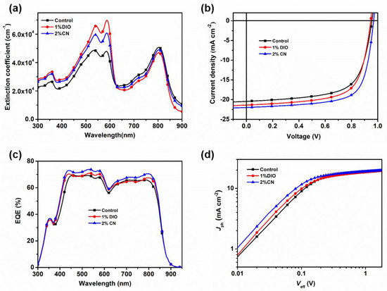
Figure 1.
(a) The extinction coefficient of the D18/PYIT-OD bilayer film fabricated from different processing conditions; (b) the representative J-V curves of devices at different solvent additives; (c) the representative EQE spectra of devices at different solvent additives; (d) the Jph–Veff curves of devices at different solvent additives.

Table 1.
Summary data of photovoltaic performance of devices with different solvent additives.
To investigate the excitons dissociation and charge collection within devices, we conducted experiments to assess the relationship between photo-generated current (Jph) and the effective voltage (Veff), as shown in Figure 1d. Here, the photo-generated current (Jph) and the effective voltage (Veff) are calculated by Jph = JL − JD and Veff = V0 − V, respectively, where JL and JD refer to the current density under illumination and dark conditions, V0 is the voltage when Jph is zero, and V is the applied voltage [28,29]. Under a large Veff, the Jph tends to be saturated (Jsat), at which point nearly all excitons are dissociated into free carriers and collected by the electrodes. We also analyzed the probability of the charge dissociation (P(E,T)) of devices under different processing conditions (Table S2), which was calculated by the ratio of Jph to Jsat under short-circuit conditions. For the devices without additives, with the addition of a 1% DIO additive and a 2% CN additive, the P(E,T) values were 89.3%, 91.4%, and 94.9%, respectively. Based on the equation Jsat = qGmaxL, we calculated the corresponding maximum exciton generation rates (Gmax) was to be 1.31 × 1028, 1.32 × 1028, and 1.38 × 1028 m−3 s−1, respectively. Devices with a 2% CN additive showed increased Gmax, which correlated well with their higher JSC, potentially contributing to the improved light absorption and more orderly molecular packing. These results demonstrate that devices with 2% CN additive exhibit superior performance in exciton and charge dynamics.
To delve into the charge recombination of different devices, we performed J-V under various light intensities (Plight) and plotted the correlation curves of JSC and VOC with Plight. The relationship between JSC and Plight follows the formula JSC ∝ (Plight)S, where S reflects the intensity of bimolecular recombination in the device. Generally, the S value being very close to the unit suggests that OSC devices experience minimal bimolecular recombination [30]. As shown in Figure 2a, for devices without an additive, with a 1% DIO additive, and with a 2% CN additive, the corresponding S values were 0.96, 0.97, and 0.98, respectively. The results indicate that devices based on D18/PYIT-OD with 2% CN are most effective in suppressing bimolecular recombination. Meanwhile, in the VOC versus Plight curves shown in Figure 2b, the controlled device exhibited the highest fitting slope, suggesting severe trap-assisted Shockley–Read–Hall (SRH) or bimolecular recombination. For the device with 1% DIO additives and 2% CN additives, the slopes were decreased to 1.60 kBT/q and 1.52 kBT/q, respectively. The smallest fitting slope for the device with the CN additive indicated that SRH or bimolecular recombination is effectively suppressed, promoting effective charge transport and collection.
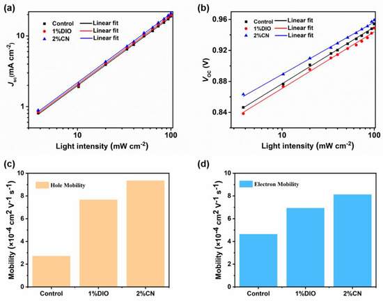
Figure 2.
(a) The relationship between JSC and Plight; (b) the relationship between VOC and Plight; (c) the hole mobility; and (d) electron mobility of the devices.
Single-carrier devices based D18/PYIT-OD bilayer films were fabricated to investigate the charge transport behavior through the space charge-limited current (SCLC) method [31], and the summarized data are listed in Table S3. The specific device structure for the hole-only device is ITO/PEDOT:PSS/D18/PYIT-OD/Ag, while the electron-only device is ITO/ZnO/D18/PYIT-OD/PFN-Br/Ag. As shown in Figure 2c,d, the hole mobility (μh) and electron mobility (μe) of the device without additive are 3.71 × 10⁻⁴ cm2 V−1 s−1 and 4.63 × 10⁻⁴ cm2 V−1 s−1, respectively. After adding additives to PYIT-OD, the measured μh increased to 7.66 × 10⁻⁴ cm2 V−1 s−1 (1% DIO) and 9.34 × 10⁻⁴ cm2 V−1 s−1 (2% CN), while the μe increased to 6.93 × 10⁻⁴ cm2 V−1 s−1 (1% DIO) and 8.18 × 10⁻⁴ cm2 V−1 s−1 (2% CN). It is evident that the device treated with the 2% CN additive not only has a more efficient charge transport performance but also a more balanced charge transport, indicating an effective reduction in charge accumulation and recombination, thereby improving the JSC of devices. In addition, exciton separation and charge transfer at the electron donor and acceptor interface are crucial for a device’s photovoltaic performance. To investigate the exciton separation and charge transfer of bilayer films, we created steady-state photoluminescence (PL) spectra of the pristine D18 film and the D18/PYIT-OD bilayer films, as shown in Figure S4. The films were excited at 467 nm, and D18 exhibited typical emission peaks at 620 and 680 nm. The PL intensity at these emission peaks was significantly quenched in the D18/PYIT-OD bilayer films, indicating efficient charge transfer at the electron donor and acceptor interface. For the bilayer film with added 2% CN, this PL quenching is most pronounced, indicating the most efficient charge transfer.
We used atomic force microscopy (AFM) to observe the influence of the type of additives and their concentrations on the surface morphology of bilayer films. As shown in Figure 3, the root-mean-square (RMS) roughness value is 1.68 nm for the bilayer film without any additives. With an increasing DIO concentration from 0.5% to 2%, the RMS roughness values rose from 1.87 nm to 3.43 nm. When the CN concentration increased from 1% to 2%, the RMS roughness values slightly decreased from 1.70 nm to 1.54 nm, exhibiting a more refined structure. However, an excessive amount of additive (3% CN concentration) led to large-scale aggregation, resulting in a sharp increase in film RMS roughness, which severely damaged device efficiency. Additionally, by examination of the transmission electron microscopy (TEM) images for both the controlled film and those added with 1% DIO and 2% CN (Figure 4), it becomes apparent that these additives precipitate morphological inhomogeneity within the film, likely attributable to the induced crystallization. Comparative analysis indicates that the addition of 2% CN results in a fiber-like film structure, leading to higher FF in the corresponding devices. This also aids in the effective separation of excitons and charge transport.
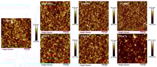
Figure 3.
AFM images of bilayer films based on D18/PYIT-OD under different processing conditions.
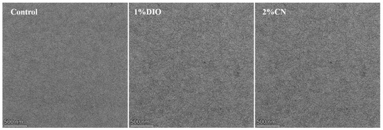
Figure 4.
TEM images of bilayer films based on D18/PYIT-OD under different processing conditions.
To gain a deeper understanding of the molecular packing and crystalline properties within the active layer, we utilized grazing-incidence wide-angle X-ray scattering (GIWAXS) measurements to examine the D18/PYIT-OD bilayer films under various processing conditions. Figure 5a shows the 2D GIWAXS patterns of D18/PYIT-OD bilayer films without any additive (control), with 1% DIO, and with 2% CN. The corresponding line-cut plots in the in-plane (IP) and out-of-plane (OOP) directions are shown in Figure 5b,c, respectively. From the 2D GIWAXS patterns under three different processing conditions, we observed a strong (010) π-π stacking peak in the OOP direction and a distinct (100) lamellar stacking peak in the IP direction. This indicates that the D18/PYIT-OD bilayer films predominantly exhibited a face-on orientation. This result also implied that the fabrication of the upper layer of PYIT-OD does not significantly alter the molecular orientation of the D18 film [32]. For the bilayer film with 1% DIO, the diffraction peak intensities are more pronounced for both the IP lamellar stacking and the OOP π-π stacking. In addition, it is evident that the bilayer film containing 2% CN exhibits a minimum full width at half maximum (FWHM) value of 0.292 Å at 1.69 Å−1 in the OOP direction, indicating strong π-π stacking. In comparison, the FWHM values for the controlled bilayer film and the film with 1% DIO are 0.352 Å and 0.317 Å, respectively. The reduced FWHM value in the film with 2% CN suggests a higher crystal coherence length (CCL). A larger CCL suggested an increase in the number of crystal repeating units within the active layer, which is more conducive to the charge transport. This is consistent with the results above where the OSC device containing 2% CN exhibited the highest hole and electron mobility. The bilayer film that incorporated the 1% DIO additive suffered from excessive aggregation, leading to a compromised photovoltaic performance of the OSC device.
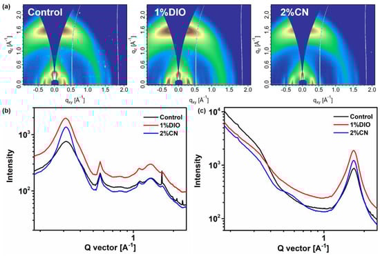
Figure 5.
(a) Two-dimensional GIWAXS patterns of bilayer films based on D18/PYIT-OD under different processing conditions; GIWAXS line-cuts of bilayer films based on D18/PYIT-OD under different processing conditions (b) in the in-plane direction and (c) in the out-of-plane direction.
3. Experimental Details
3.1. Materials
The D18 polymer and the non-fullerene polymer acceptor PYIT-OD were purchased from Derthon Optoelectronics Materials Science Technology Co., Ltd. (Shenzhen, China). Other reagents and solvents were purchased from commercial sources and used without any further treatment.
3.2. Device Fabrication
The solution-processed layer-by-layer solar cells devices were fabricated with a conventional structure of Indium tin oxide (ITO)/PEDOT:PSS/D18/L PYIT-OD/PDIN/Ag and the fabrication details are as follows: ITO coated glass substrates were cleaned prior to device fabrication by sonication in acetone, detergent, distilled water, and isopropyl alcohol. After being treated with an oxygen plasma for 20 min, 40 nm thick poly(styrene sulfonate)-doped poly(ethylene-dioxythiophene) (PEDOT:PSS) (Bayer Baytron 4083) layer was spin-casted on the ITO-coated glass substrates at 3000 rpm for 30 s, the substrates were subsequently dried at 150 °C for 10 min in air and then transferred to a N2 glovebox. The donor and acceptor were dissolved in chloroform (CF) with the concentration of 5 mg/mL and 7 mg/mL, respectively. The D18 solution was stirred at 100 °C for 30 min, followed by stirring at 40 °C for 2 h. After the D18 had completely dissolved in CF, spin-coating with the speed of 3000 rpm at a fixed temperature of 40 °C was performed on the prepared substrate with PEDOT:PSS. The PYIT-OD solution was stirred at 60 °C for 1 h, and then spin-coated at room temperature. The spin-coating conditions were 4000 rpm for 40 s. The thickness of the active layer was 110 nm. PDIN layer was deposited by spin casting from 2 mg/mL solution in methanol. Finally, Ag (~90 nm) was evaporated with a shadow mask as the top electrode. The effective area was measured to be 0.0516 cm2.
3.3. Measurements and Instruments
UV-vis-NIR spectra of pure and blend films on a quartz substrate were recorded at room temperature (ca. 25 °C) using a UV-3600 Plus UV-Vis-NIR spectrometer. Photoluminescence spectra were recorded on a Horiba Nanolog fluorescence spectrophotometer. PCEs were determined from J-V characteristics measured by a Keithley 2400 source-measurement unit under AM 1.5G spectrum from a solar simulator (Oriel model 91192). Solar simulator illumination intensity was determined using a monocrystal silicon reference cell (Hamamatsu S1133, with KG-5 visible color filter) calibrated by the National Renewable Energy Laboratory (NREL). External quantum efficiency (EQE) values of the encapsulated devices were measured by using an integrated system (Enlitech, Kaohsiung City, Taiwan) and a lock-in amplifier with a current preamplifier under short-circuit conditions. The devices were illuminated by monochromatic light from a 75 W xenon lamp. The light intensity was determined by using a calibrated silicon photodiode. Steady-state photoluminescence tests were performed using a Fluorolog 3 spectrofluorometer (HORIBA Instruments Incorporated, Kyoto, Japan). The Transient absorption (TA) spectra were collected by a home-built TA system described briefly as below. The fs laser from an amplifier (800 nm, 1 KHz, Legend Elite F 1K HE+II, Coherent, Saxonburg, PA, USA) was used as the light source. The output from the amplifier (800 nm) or a doubled frequency (400 nm) were employed as the pump light. For the pump light, “on” and “off” were regulated by a mechanical chopper (500 Hz, MC2000B-EC, Thorlabs, Newton, NJ, USA) in the pump beam. The supercontinuum white light generated by a 3 mm thick sapphire plate was used as the probe light, which was then collected by a spectrometer (300 nm–1100 nm, Omni-λ200i, Zolix, Beijing, China). The delay between the probe light and the pump light is controlled by a mechanical delay stage. The atomic force microscopy (AFM) measurements of the surface morphology of D18 films were conducted on a Dimension Icon Scanning Probe Microscope system.
3.4. Charge Carrier Mobility Measurement
Hole and electron mobilities were measured by the space-charge limited current (SCLC) method with the hole-only device structure of ITO/PEDOT:PSS/D18/PYIT-OD/Ag and ITO/ZnO/D18/PYIT-OD/PFN-Br/Ag electron-only devices, respectively. The active layers for these devices were spin-coated under the same condition as that of solar cells. J–V curves in the range of −4 to 4 V were gained by a Keithley 2400 source-measure unit in dark conditions. The mobilities were obtained by fitting J–V curves with the formula of:
where J is the current density, L is the thickness of the active layer, μ is the mobility, εo is the vacuum dielectric constant, εr is the relative dielectric constant of the transport medium, and V (Vapp − Vbi) is the internal voltage, where Vapp is the applied voltage and Vbi is the built-in voltage.
J = 9εoεrµV2/(8L3)
4. Conclusions
In conclusion, LBL all-PSCs based on the D18/PYIT-OD were fabricated by incorporating solvent additives into the PYIT-OD acceptors to regulate the appropriate microstructure. CN and DIO additives have a significant impact on the molecular packing and morphology of the active layer. With the optimized amount of additives, both CN and DIO can significantly enhance the photovoltaic performance of the devices, particularly CN, which is very effective in improving the JSC and FF. The presence of additives also affects the crystallization and packing of D18, thereby affecting the charge mobility of the devices. In addition, devices containing a 2% CN additive experienced a significant increase in exciton separation, and a marked reduction in bimolecular recombination and trap-assisted recombination. Finally, a morphological study confirmed that the presence of additives significantly improves the molecular crystallization and packing of the active layer, resulting in enhanced crystallinity and CCL. As a result, the optimized LBL all-PSCs based on the D18/PYIT-OD delivered a high PCE of 15.07%. The strategy of separately regulating the morphology of the electron donor and acceptor layers via the LBL fabrication method makes it a very promising approach to promote the development of organic photovoltaic technology.
Supplementary Materials
The following supporting information can be downloaded at: https://www.mdpi.com/article/10.3390/molecules29122879/s1, Figure S1 Chemical structures of D18 and PYIT-OD. Figure S2 J-V curves of devices at different solvent additives concentration. Figure S3 EQE curves of devices at different solvent additives concentration. Figure S4 PL spectra of the pristine D18 film and the D18/PYIT-OD bilayer films. Table S1 Photovoltaic parameters for D18/PYIT-OD-based all-PSCs. Table S2 The parameters of exciton dissociation efficiency and Gmax of devices obtained from different processing conditions. Table S3 Summary of the fitting data for hole-only and electron-only devices.
Author Contributions
Conceptualization, L.X.; Data curation, Y.W.; Writing—original draft, Y.W., P.L. and S.Y.; Writing—review & editing, Y.M.; Supervision, L.X.; Project administration, L.X. All authors have read and agreed to the published version of the manuscript.
Funding
L.X. and was supported by the financial support from the National Natural Science Foundation of China (51903057) and the Guangzhou Basic and Applied Basic Research Foundation (2023A04J0349). We also thank the support from the National Key Research and Development Program of China (2020YFB0408100) and Analysis and Test Center of Guangdong University of technology for the UV-vis-NIR and PL spectroscopy measurement.
Institutional Review Board Statement
Not applicable.
Informed Consent Statement
Not applicable.
Data Availability Statement
Data are contained within the article and Supplementary Materials.
Conflicts of Interest
The authors declare no conflict of interest.
References
- Xiao, L.; Wu, X.; Ren, G.; Kolaczkowski, M.A.; Huang, G.; Tan, W.; Ma, L.; Liu, Y.; Peng, X.; Min, Y. Highly efficient ternary solar cells with efficient förster resonance energy transfer for simultaneously enhanced photovoltaic parameters. Adv. Funct. Mater. 2021, 31, 2105304. [Google Scholar] [CrossRef]
- Yi, J.; Zhang, G.; Yu, H.; Yan, H. Advantages, challenges and molecular design of different material types used in organic solar cells. Nat. Rev. Mater. 2024, 9, 46–62. [Google Scholar] [CrossRef]
- Peng, S.; Luo, J.; Li, P.; Xiao, L.; Yang, C.; Jin, Y.; Lin, R.; Huo, Y.; Liu, Y.; Min, Y. Adding the third component with similar building blocks to regulate the miscibility of active layer enables high efficient ternary solar cells. Chem. Eng. J. 2023, 474, 145501. [Google Scholar] [CrossRef]
- Zhang, H.; Jia, S.; Liu, Z.; Chen, Z. Ternary Organic Solar Cells by Small Amount of Efficient Light Absorption Polymer PSEHTT as Third Component Materials. Molecules 2023, 28, 6832. [Google Scholar] [CrossRef] [PubMed]
- Yu, G.; Gao, J.; Hummelen, J.C.; Wudl, F.; Heeger, A.J. Polymer photovoltaic cells: Enhanced efficiencies via a network of internal donor-acceptor heterojunctions. Science 1995, 270, 1789–1791. [Google Scholar] [CrossRef]
- Lin, Y.; Wang, J.; Zhang, Z.G.; Bai, H.; Li, Y.; Zhu, D.; Zhan, X. An electron acceptor challenging fullerenes for efficient polymer solar cells. Adv. Mater. 2015, 27, 1170–1174. [Google Scholar] [CrossRef] [PubMed]
- He, Z.; Xiao, B.; Liu, F.; Wu, H.; Yang, Y.; Xiao, S.; Wang, C.; Russell, T.P.; Cao, Y. Single-junction polymer solar cells with high efficiency and photovoltage. Nat. Photonics 2015, 9, 174–179. [Google Scholar] [CrossRef]
- Han, C.; Wang, J.; Zhang, S.; Chen, L.; Bi, F.; Wang, J.; Yang, C.; Wang, P.; Li, Y.; Bao, X. Over 19% efficiency organic solar cells by regulating multidimensional intermolecular interactions. Adv. Mater. 2023, 35, 2208986. [Google Scholar] [CrossRef] [PubMed]
- Zhu, L.; Zhang, M.; Xu, J.; Li, C.; Yan, J.; Zhou, G.; Zhong, W.; Hao, T.; Song, J.; Xue, X. Single-junction organic solar cells with over 19% efficiency enabled by a refined double-fibril network morphology. Nat. Mater. 2022, 21, 656–663. [Google Scholar] [CrossRef]
- Liu, K.; Jiang, Y.; Liu, F.; Ran, G.; Huang, F.; Wang, W.; Zhang, W.; Zhang, C.; Hou, J.; Zhu, X. Organic Solar Cells with Over 19% Efficiency Enabled by a 2D-Conjugated Non-fullerene Acceptor Featuring Favorable Electronic and Aggregation Structures. Adv. Mater. 2023, 35, 2300363. [Google Scholar] [CrossRef]
- McDowell, C.; Abdelsamie, M.; Toney, M.F.; Bazan, G.C. Solvent additives: Key morphology-directing agents for solution-processed organic solar cells. Adv. Mater. 2018, 30, 1707114. [Google Scholar] [CrossRef] [PubMed]
- Meng, L.; Wu, S.; Wan, X.; Shen, Z.; Li, M.; Yang, Y.; Wang, J.; Lu, G.; Ma, Z.; Yao, Z. Tuning the Phase Separation by Thermal Annealing Enables High-Performance All-Small-Molecule Organic Solar Cells. Chem. Mater. 2022, 34, 3168–3177. [Google Scholar] [CrossRef]
- Hou, Y.; Wang, Q.; Huang, C.; Yang, T.; Shi, S.; Yao, S.; Ren, D.; Liu, T.; Zhang, G.; Zou, B. Controlling the Treatment Time for Ideal Morphology towards Efficient Organic Solar Cells. Molecules 2022, 27, 5713. [Google Scholar] [CrossRef] [PubMed]
- Sun, Y.; Welch, G.C.; Leong, W.L.; Takacs, C.J.; Bazan, G.C.; Heeger, A.J. Solution-processed small-molecule solar cells with 6.7% efficiency. Nat. Mater. 2012, 11, 44–48. [Google Scholar] [CrossRef] [PubMed]
- Li, X.; Du, X.; Zhao, J.; Lin, H.; Zheng, C.; Tao, S. Layer-by-Layer Solution Processing Method for Organic Solar Cells. Sol. RRL 2021, 5, 2000592. [Google Scholar] [CrossRef]
- Li, M.; Wang, Q.; Liu, J.; Geng, Y.; Ye, L. Sequential deposition enables high-performance nonfullerene organic solar cells. Mater. Chem. Front. 2021, 5, 4851–4873. [Google Scholar] [CrossRef]
- Wei, Y.; Chen, Z.; Lu, G.; Yu, N.; Li, C.; Gao, J.; Gu, X.; Hao, X.; Lu, G.; Tang, Z. Binary organic solar cells breaking 19% via manipulating the vertical component distribution. Adv. Mater. 2022, 34, 2204718. [Google Scholar] [CrossRef] [PubMed]
- Chen, H.; Zhao, T.; Li, L.; Tan, P.; Lai, H.; Zhu, Y.; Lai, X.; Han, L.; Zheng, N.; Guo, L.; et al. 17.6%-Efficient Quasiplanar Heterojunction Organic Solar Cells from a Chlorinated 3D Network Acceptor. Adv. Mater. 2021, 33, 2102778. [Google Scholar] [CrossRef] [PubMed]
- Li, X.; Yang, H.; Du, X.; Lin, H.; Yang, G.; Zheng, C.; Tao, S. High-performance layer-by-layer organic solar cells enabled by non-halogenated solvent with 17.89% efficiency. Chem. Eng. J. 2023, 452, 139496. [Google Scholar] [CrossRef]
- Zhang, Y.; Wu, B.; He, Y.; Deng, W.; Li, J.; Li, J.; Qiao, N.; Xing, Y.; Yuan, X.; Li, N. Layer-by-layer processed binary all-polymer solar cells with efficiency over 16% enabled by finely optimized morphology. Nano Energy 2022, 93, 106858. [Google Scholar] [CrossRef]
- Xu, X.; Yu, L.; Meng, H.; Dai, L.; Yan, H.; Li, R.; Peng, Q. Polymer Solar Cells with 18.74% Efficiency: From Bulk Heterojunction to Interdigitated Bulk Heterojunction. Adv. Funct. Mater. 2022, 32, 2108797. [Google Scholar] [CrossRef]
- Wu, X.; Wu, Y.; Peng, S.; Xiao, L.; Xiao, Z.; Zhang, W.; Ren, G.; Min, Y.; Liu, Y. Layer-by-Layer-Processed Organic Solar Cells with 18.02% Efficiency Enabled by Regulating the Aggregation of Bottom Polymers. Sol. RRL 2023, 7, 2300136. [Google Scholar] [CrossRef]
- Yang, X.; Li, B.; Zhang, X.; Li, S.; Zhang, Q.; Yuan, L.; Ko, D.H.; Ma, W.; Yuan, J. Intrinsic Role of Volatile Solid Additive in High-Efficiency PM6: Y6 Series Nonfullerene Solar Cells. Adv. Mater. 2023, 35, 2301604. [Google Scholar] [CrossRef] [PubMed]
- Ma, Y.-F.; Zhang, Y.; Zhang, H.-L. Solid additives in organic solar cells: Progress and perspectives. J. Mater. Chem. C. 2022, 10, 2364–2374. [Google Scholar] [CrossRef]
- Song, X.; Gasparini, N.; Baran, D. The Influence of Solvent Additive on Polymer Solar Cells Employing Fullerene and Non-Fullerene Acceptors. Adv. Electron. Mater. 2018, 4, 1700358. [Google Scholar] [CrossRef]
- Liu, X.; Li, X.; Wang, L.; Fang, J.; Yang, C. Synergistic effects of the processing solvent and additive on the production of efficient all-polymer solar cells. Nanoscale 2020, 12, 4945–4952. [Google Scholar] [CrossRef] [PubMed]
- Song, J.; Zhu, L.; Li, C.; Xu, J.; Wu, H.; Zhang, X.; Zhang, Y.; Tang, Z.; Liu, F.; Sun, Y. High-efficiency organic solar cells with low voltage loss induced by solvent additive strategy. Matter 2021, 4, 2542–2552. [Google Scholar] [CrossRef]
- Ma, Y.; Cai, D.; Wan, S.; Wang, P.; Wang, J.; Zheng, Q. Ladder-Type Heteroheptacenes with Different Heterocycles for Nonfullerene Acceptors. Angew. Chem. Int. Edit. 2020, 132, 21811–21817. [Google Scholar] [CrossRef]
- Hu, K.; Du, J.; Zhu, C.; Lai, W.; Li, J.; Xin, J.; Ma, W.; Zhang, Z.; Zhang, J.; Meng, L.; et al. Chlorinated polymerized small molecule acceptor enabling ternary all-polymer solar cells with over 16.6% efficiency. Sci. China Chem. 2022, 65, 954–963. [Google Scholar] [CrossRef]
- Dong, S.; Zhang, K.; Liu, X.; Yin, Q.; Yip, H.-L.; Huang, F.; Cao, Y. Efficient organic-inorganic hybrid cathode interfacial layer enabled by polymeric dopant and its application in large-area polymer solar cells. Sci. China Chem. 2019, 62, 67–73. [Google Scholar] [CrossRef]
- Xiao, L.; Kolaczkowski, M.A.; Min, Y.; Liu, Y. Substitution effect on thiobarbituric acid end groups for high open-circuit voltage non-fullerene organic solar cells. ACS. Appl. Mater. Interfaces 2020, 12, 41852–41860. [Google Scholar] [CrossRef] [PubMed]
- Xiao, M.; Meng, Y.; Tang, L.; Li, P.; Tang, L.; Zhang, W.; Hu, B.; Yi, F.; Jia, T.; Cao, J.; et al. Solid Additive-Assisted Selective Optimization Strategy for Sequential Deposited Active Layers to Construct 19.16% Efficiency Binary Organic Solar Cells. Adv. Funct. Mater. 2024, 34, 2311216. [Google Scholar] [CrossRef]
Disclaimer/Publisher’s Note: The statements, opinions and data contained in all publications are solely those of the individual author(s) and contributor(s) and not of MDPI and/or the editor(s). MDPI and/or the editor(s) disclaim responsibility for any injury to people or property resulting from any ideas, methods, instructions or products referred to in the content. |
© 2024 by the authors. Licensee MDPI, Basel, Switzerland. This article is an open access article distributed under the terms and conditions of the Creative Commons Attribution (CC BY) license (https://creativecommons.org/licenses/by/4.0/).