Article

Insight into the Role of Rb Doping for Highly Efficient Kesterite Cu2ZnSn(S,Se)4 Solar Cells

1
Key Laboratory of Functional Materials Physics and Chemistry of the Ministry of Education, Jilin Normal University, Siping 136000, China
2
State Key Laboratory of Superhard Materials, College of Physics, Jilin University, Changchun 130012, China
3
Key Laboratory of Physics and Technology for Advanced Batteries (Ministry of Education), College of Physics, Jilin University, Changchun 130012, China
*
Authors to whom correspondence should be addressed.
Molecules 2024, 29(15), 3670; https://doi.org/10.3390/molecules29153670
Submission received: 15 July 2024 / Revised: 30 July 2024 / Accepted: 31 July 2024 / Published: 2 August 2024
(This article belongs to the Special Issue Preparation and Application of Key Materials for Solar Cells)

Abstract

:
Various copper-related defects in the absorption layer have been a key factor impeding the enhancement of the efficiency of Cu2ZnSn(S,Se)4 (CZTSSe) solar cells. Alkali metal doping is considered to be a good strategy to ameliorate this problem. In this article, Rb-doped CZTSSe (RCZTSSe) thin films were synthesized using the sol–gel technique. The results show that the Rb atom could successfully enter into the CZTSSe lattice and replace the Cu atom. According to SEM results, a moderate amount of Rb doping aided in enhancing the growth of grains in CZTSSe thin films. It was proven that the RCZTSSe thin film had the densest surface morphology and the fewest holes when the doping content of Rb was 2%. In addition, Rb doping successfully inhibited the formation of CuZn defects and correlative defect clusters and promoted the electrical properties of RCZTSSe thin films. Finally, a remarkable power conversion efficiency of 7.32% was attained by the champion RCZTSSe device with a Rb content of 2%. Compared with that of un-doped CZTSSe, the efficiency improved by over 30%. This study offers new insights into the influence of alkali metal doping on suppressing copper-related defects and also presents a viable approach for improving the efficiency of CZTSSe devices.

1. Introduction

To achieve a cleaner carbon-neutral future and promote the production of sustainable green energy, abundant, environmentally friendly and non-toxic CZTSSe thin-film solar cells have emerged and are highly competitive among next-generation photovoltaic (PV) technology [1,2,3,4,5]. In addition, kesterite CZTSSe compounds have also been receiving more and more attention because of a higher absorption coefficient (~104 cm−1) and adjustable bandgap energy. However, compared to the Shockley–Queisser limit theoretical efficiency (32.2%) [6], current CZTSSe photovoltaic cells only achieve a certified efficiency of 14.9% [7]. Compared to that of other photovoltaic devices, CZTSSe solar cells have a lower open-circuit voltage (Voc) [8,9,10], limiting their further widespread application. The main reason for the formation of low open-circuit voltage is the band tail states emerging from a significant amount of CuZn defects and [2CuZn + SnZn] defect clusters [11,12,13,14,15].
Investigations have revealed that cationic doping and heterojunction annealing can optimize device performance [16,17,18]. In recent years, cationic doping of alkali metal elements has been validated as a successful strategy for enhancing the PCE of CZTSSe devices [19,20,21]. Studies have also shown that Li, Na, and K elements can be successfully doped into the CZTSSe crystal structure and thus reduce Voc loss and improve cell efficiency. Rubidium, as the same main group element, is known as an effective dopant in enhancing the performance of Cu(In,Ga)Se2 (CIGS) thin-film photovoltaic devices [22,23]. However, in the domain of CZTSSe, rubidium-doped CZTSSe have only been prepared by magnetron sputtering. Wu et al. prepared CZTSSe thin films with different Rb content by magnetron sputtering, and proved that Rb doping can reduce the formation of the high-resistance ZnSe phase and improve device efficiency [24]. Compared with magnetron sputtering, the sol–gel method is one of the simple, economically, and efficient methods, and has its own advantages like low processing temperature, non-vacuum processing conditions, and homogeneity of the produced material. However, there have been no studies conducted on the synthesis of the RCZTSSe absorption layer material using the sol–gel technique, and the effect of Rb doping on the efficiency of CZTSSe devices so far.
In this study, we successfully synthesized high-quality RCZTSSe thin films through a straightforward sol–gel technique. The characteristics of the RCZTSSe thin films, including their structure, optical properties, and electrical behavior, were thoroughly examined. The results show that the applicable content of Rb doping could enhance the quality of the crystallization of the absorption layer and carrier mobility. Moreover, the doping of a small amount of Rb could further suppress the formation of CuZn defects and correlative defect clusters. When the content of Rb was 2%, device efficiency reached 7.32% and open circuit voltage increased to 379.69 mV.

2. Results and Discussion

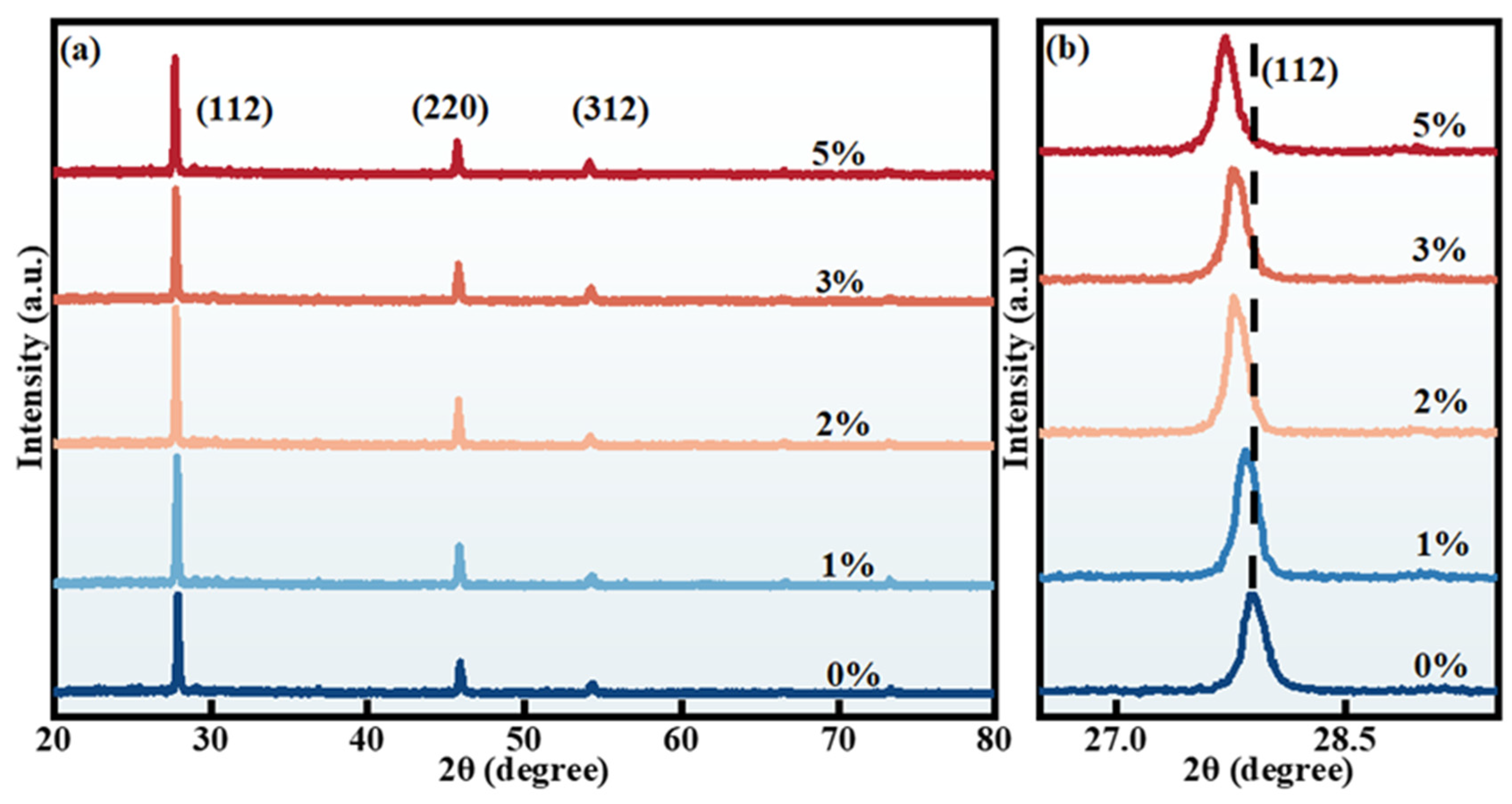
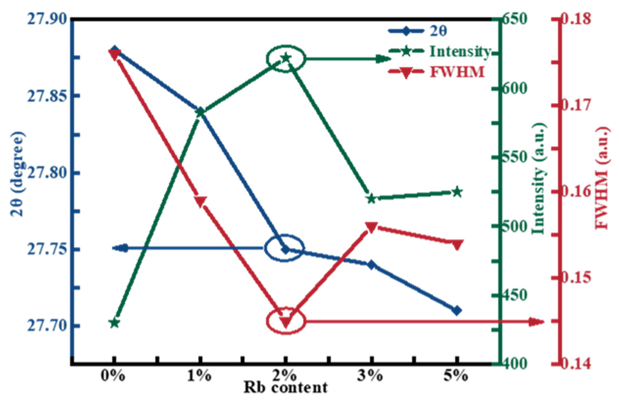
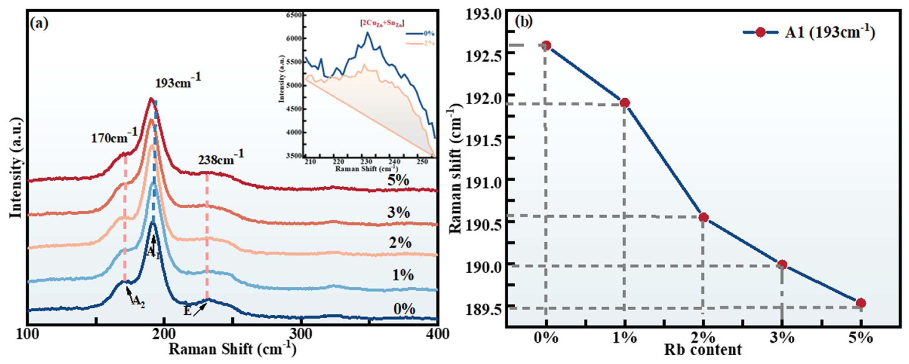
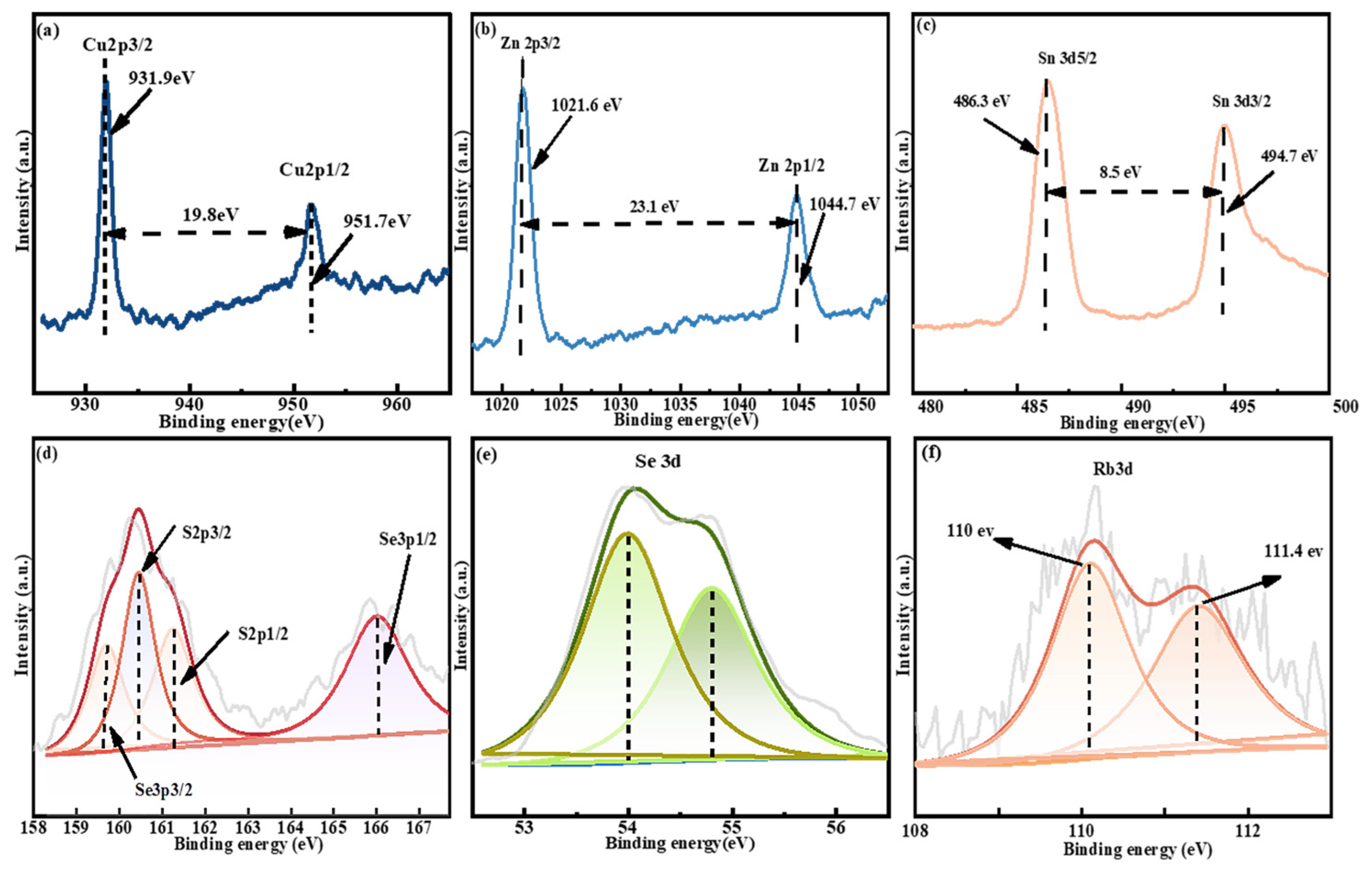
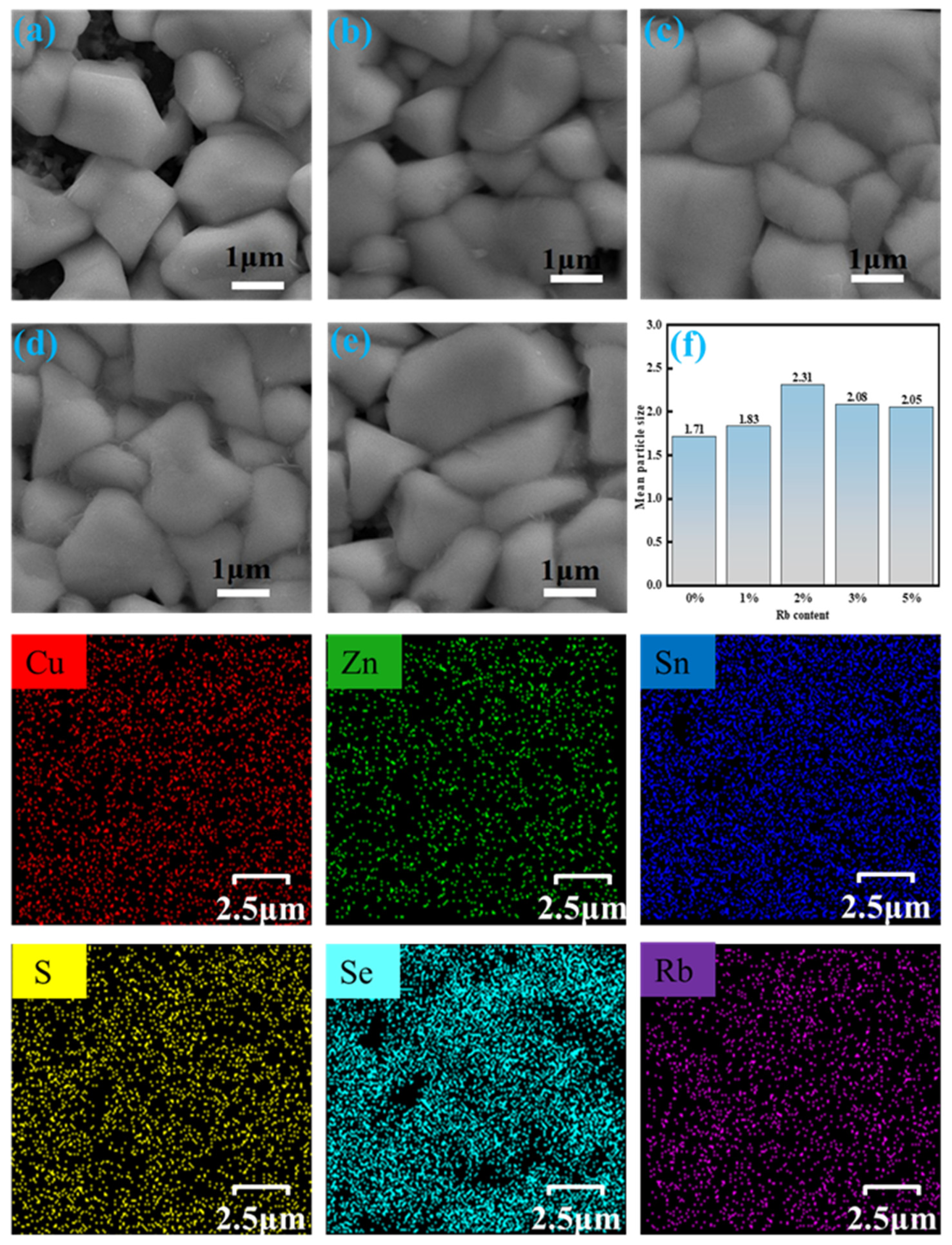
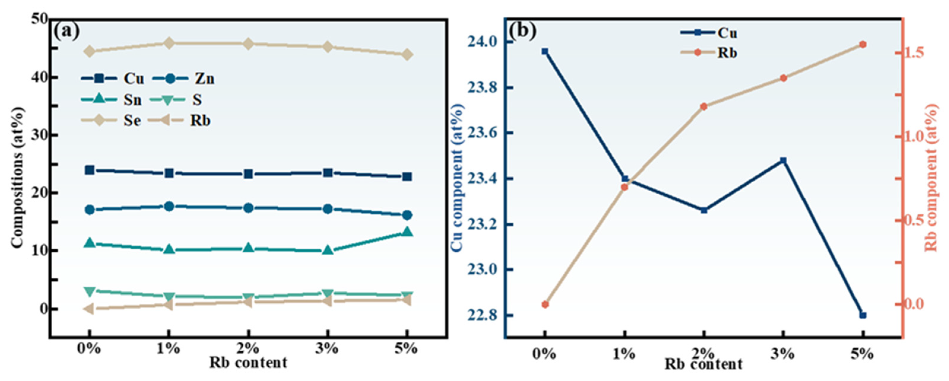
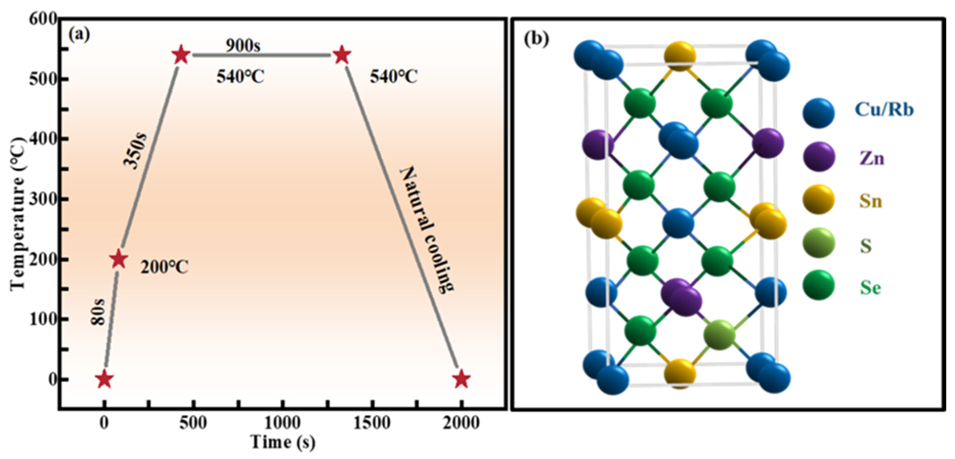
2.1. Structural Characterization

Firstly, XRD data of RCZTSSe thin films with diverse Rb-doping content were analyzed. The results are shown in Figure 1a. In the following, for convenience of description, Rb-0%, Rb-1%, Rb-2%, Rb-3%, and Rb-5% were used to represent the un-doped sample and the doped samples with 1%, 2%, 3%, and 5% of Rb-doping content, respectively. XRD diffraction peaks of all films were located at 27.20°, 45.26°, and 53.39°, corresponding to (112), (220), and (312) crystallographic planes of CZTSSe, respectively [25]. Besides the three peaks above, other diffraction peaks of copper-, zinc-, selenium-, and rubidium-related complexes were not observed, indicating that Rb atoms entered the crystal lattice in the form of replacing Cu atoms or gap atoms, and no impurity phase was formed on the film surface. Figure 1b shows the corresponding enlarged image of the (112) diffraction peaks. When the Rb-doping content increased from 0% to 5%, the diffraction peak moved towards a smaller angle. The reason was that the Rb+ ion’s radius (1.52 Å) surpassed that of the Cu+ ion (0.77 Å), and the replacement of Cu+ by Rb+ ion was the cause of the expansion of the volume of a single crystal cell.
To further research the effect of Rb-doping content on the crystal quality of CZTSSe thin films, the full width at half maximum (FWHM), the diffraction angle 2θ, and the intensity of the peak were obtained from the (112) peak in the XRD spectrum, as shown in Figure 2. The slight shift of the (112) diffraction peak toward a smaller angle was observed with the Rb content increasing. It was because the replacement of smaller Cu+ ions by larger Rb+ ions [26]. When the Rb-doping content was in the range of 0% to 2%, the (112) peak intensity of the film displayed an increasing tendency, and FWHM fell from 0.176 to 0.145, indicating that the crystallinity increased with increasing Rb content. However, as the doping content continue to rise, the intensity of the (112) peak reduced, and FWHM increased gradually, indicating that the crystallinity of the absorbed layer decreased. It was concluded that the crystallinity of the film samples was optimal when the Rb-doping content was 2%.
According to the XRD results, the crystal lattice parameters were calculated by using the Bragg equation, and the influence of Rb doping on the crystal structure was discussed. The Bragg equation for tetragonal crystal materials such as CZTSSe can be expressed in terms of the Miller index (hkl) [27]:
sin θ 2 = λ 2 4 a 2 ( h 2   +   k 2 )   +   l 2
The Bragg equation was utilized in conjunction with Equation (1) to obtain Equation (2), and the ultimate lattice constant is denoted by Equation (3):
2dhklsinθ = nλ
1 d 2 hkl = h 2 + k 2 a 2 + 1 2 c 2
In the formula, dhkl represents lattice spacing (hkl). The lattice constant a can be ascertained from the (220) plane, while the lattice constant c is derivable from the (112) plane. Figure 3a displays the lattice constants of the RCZTSSe films with various Rb contents of 0%, 1%, 2%, 3%, and 5%. It can be seen that when Rb-doping content increased, a escalated from 5.61 Å to 5.62 Å and c increased from 10.56 Å to 10.91 Å. It was due to Rb+ having a bigger ionic radius that primarily occupied the site of Cu+, which has a smaller ionic radius, in the RCZTSSe thin film, leading to an increase in the lattice constant [28], which was consistent with XRD results. In order to prove the structure of the RCZTSSe film, Figure 3b displays the lattice parameters η and volume V of the RCZTSSe film. According to previous reports, when the lattice parameter η is less than or equal to 1, the corresponding CZTSSe-based film sample exhibits a kesterite structure. Figure 3b demonstrates that the η value of RCZTSSe remained below 1 as Rb content increased from 0% to 5%. It is indicated that the crystal structure of the thin film remained unchanged after Rb doping. Furthermore, the V value increased with increasing Rb-doping content due to the larger ionic radius of Rb+ compared to that of Cu+, providing further evidence of successful Rb doping into the CZTSSe lattice.
However, although no diffraction peak of secondary phases was found in the XRD spectrum, the existence of Cu2SnS3, Cu2SnSe3, ZnSe, and ZnS impurity phases still could not be ruled out due to their diffraction peaks coinciding with those of CZTSSe. Therefore, Raman scattering was used as an auxiliary method to detect these possible impurity phases. Shown in Figure 4a, the significant vibrations at 170, 193, and 238 cm−1 in the Raman spectra are closely related to CZTS and CZTSe and are characteristic modes (A2, A1, and E) of the kesterite structure, respectively [29]. Therefore, all peaks appearing in the spectra were associated with CZTSSe materials, and other impurity phases were not found.
In addition, a change in Raman peak intensity can reflect the variation in defect clusters in CZTSSe. The variation of peak intensity at 236 cm−1 is positively correlated with the defect concentration of the [2CuZn + SnZn] defect clusters [30,31]. The illustration in Figure 4a shows the enlarged Raman spectra of Rb-0% and Rb-2% samples in the range of 210–255 cm−1. Comparing with that of the Rb-0% film, the peak intensity of the Rb-2% thin film at 236 cm−1 diminished slightly, suggesting a reduction of the adverse [2CuZn + SnZn] defect cluster density. Combined with XRD and Raman analyses, it was found that Rb doped into the lattice of CZTSSe could impede the formation of detrimental deep-level defects by occupying Cu position individually. Figure 4b reveals the change of the peak position of the A1 vibration mode with Rb-doping content, so as to explore the impact of Rb-doping content on the Raman spectrum. As the content of Rb doping increased from 0% to 5%, the primary Raman peak of the RCZTSSe films exhibited a red shift. It was because larger Rb ions were incorporated into the CZTSSe lattice, resulting in lattice expansion, which led to changes in atomic vibration. These findings are consistent with the results from XRD analysis.
Subsequently, to ascertain the valence states of Cu, Zn, Sn, S, Se, and Rb in RCZTSSe, we employed XPS measurements, illustrated in Figure 5. After cation replacement, the valence states of Cu(+1) and Zn(+2) can be determined from the peak positions and energy differences in the Cu 2p and Zn 2p spectra shown in Figure 5a,b [32,33]. The XPS spectrum of Sn 3d is depicted in Figure 5c. Two independent peaks situated at 486.3 eV and 494.7 eV were consistent with the core energy levels of Sn 3d5/2 and Sn 3d3/2, respectively. This suggests that Sn is in a +4 valence state [34]. Since the fitting curve of S 2p nearly overlapped with that of Se 3p, the S 2p XPS spectrum was acquired using Gaussian fitting techniques, as shown in Figure 5d. These characteristic peaks obtained after fitting were matched with Se 2p3/2, S 2p3/2, S 2p1/2, and Se 3p1/2. The peak values of S 2p3/2 and S 2p1/2 were 160.5 eV and 161.3 eV, respectively, within the established range of standard values for S in sulfide compounds. Consequently, it was deduced that S was present as S2− in RCZTSSe [35]. Figure 5e shows that the peaks of Se 3d3/2 and Se 3d1/2, identified using the Gauss-Lorentz fitting technique, were positioned at 54.8 and 54.0 eV, respectively. This indicates that Se ions were present in the form of Se2− in RCZTSSe [36]. Figure 5f also shows the existence of Rb in the film. Rb 3d peaks were recorded at 110 eV and 110.4 eV, and its binding energy was nearly equivalent to that of Rb+. It indicated that the valence state of Rb was +1 [37]. Therefore, the XPS results showed that Rb was successfully doped into CZTSSe, and the composition elements of RCZTSSe film samples were obtained in the chemical valence states of Cu+, Zn2+, Sn4+, S2−, Se2−, and Rb+1.
A high-quality CZTSSe absorbing layer with high crystallinity and a smooth and dense morphology is also key to achieving high-performance devices [38]. Therefore, we ulteriorly studied the effect of Rb doping on the growth of grains. In Figure 6, the morphology of RCZTSSe films characterized by SEM is shown. It is clearly discernible from Figure 6a–e that the dimension of the grains of all RCZTSSe film samples increased compared with that of the un-doped CZTSSe film sample [39]. The Rb-0% thin film sample had a rough surface, small grain size, and many holes. The existence of holes may hinder the transfer of charge, which harmfully influences the performance of the device. When the doping amount of Rb increased from 0% to 2%, the film sample became inceasingly flatter, denser, and smoother. It is observable in Figure 6f that the average grain dimension of the Rb-2% thin film sample was the largest. It has been reported that in the early selenization process, the elements of alkali metals in the precursor film can potentially react with Se to form alkali metal–Se liquid phase melts. These liquid phase melts can hasten the spread of Cu, Zn, and Sn ions, thereby improving the crystallinity of the absorption layer and passivating the grain boundaries [40,41]. Thus, in the present work, a Rb–Se liquid phase may have been generated after Rb doping, which was conducive to the change of film sample morphology and the inhibition of recombination loss at the grain boundary. However, Figure 6d,e shows that with an incremental rise in Rb content, the surface of the film progressively became coarse, and voids also increased, which was inconvenient to carrier transport [42]. Therefore, suitable Rb doping can enhance grain development, improve the morphology of the film, and aid in the preparation of efficient RCZTSSe solar cells. Finally, we found that when the doping content of Rb was 2%, the surface of the RCZTSSe thin film was exceptionally flat, smooth, and highly compact. Additionally, the elements distribution diagram of the Rb-2% thin film measured by EDS is shown in Figure 6. It can be observed that Cu, Zn, Sn, S, Se, and Rb were evenly distributed in RCZTSSe.
Element composition alteration in the film is very important to crystallinity and the distribution of RCZTSSe defects. Using EDS, the constitution and distribution of elements in the film were analyzed. Table 1 enumerates the actual element composition in RCZTSSe with various Rb-doping contents detected by EDS. It is shown in Table 1 that the Rb/(Rb + Cu) ratios in the films increased with the increasing Rb doping ratio in the solutions. This indicates that the atomic proportion Rb/(Rb + Cu) of RCZTSSe could be modified through altering the chemical proportions of the solutions. Every sample demonstrated Cu-poor and Zn-rich proportions. As is common knowledge, the Cu-poor and Zn-rich ratio can enhance the formation VCu and restrain the formation of CuZn, which have the effect of maximizing the PCE of CZTSSe devices [43].
Figure 7a displays the EDS outcomes of the RCZTSSe films, also shown in Table 1. The findings indicate that with an increasing Rb doping ratio, the content of other elements except Cu in the film were finally actually unchanged. Figure 7b demonstrates that the proportion of Cu atoms decreased when the content of Rb gradually increased. The above results indicate that Rb doped into the CZTSSe lattice by substituting the partial Cu atom.

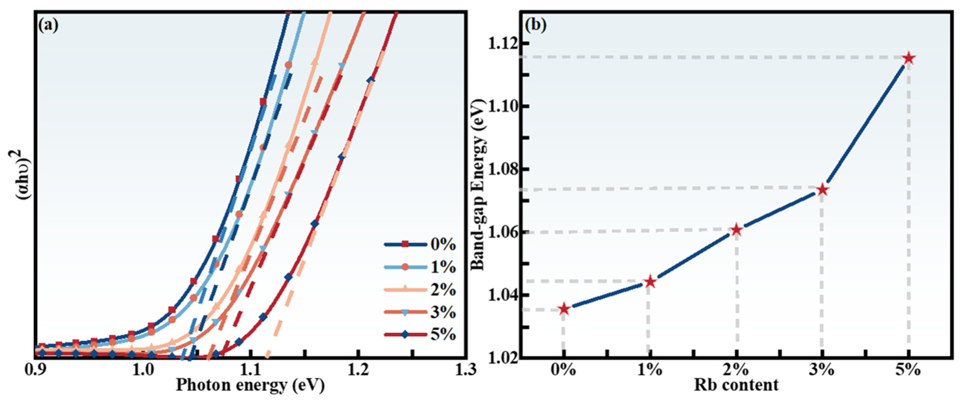
2.2. Photoelectric Characteristics

For the purpose of investigating the impact of Rb-doping content on the optical bandgap (Eg) of RCZTSSe thin films, a UV–Vis–NIR spectrophotometer was utilized to examine the absorption spectra of the RCZTSSe films. Figure 8a shows the (αhυ)2-hυ curve of the RCZTSSe films with diverse Rb-doping content. The optical Eg value of RCZTSSe was determined using the Tauc equation, based on the solid-state energy band theory [44]:
αhυ = B(hυ − Eg)n
where α, hυ, and B are the absorption coefficient, photon energy, and Planck’s constant, respectively [45]. Theoretical research suggests that for permitted direct transition, permitted indirect transition, prohibited direct transition, and prohibited indirect transition semiconductors, the corresponding values of n are 1/2, 3/2, 2, and 3, respectively. RCZTSSe films are direct bandgap semiconductors, therefore, n was 1/2. The correlation between α and the bandgap can be expressed with the listed formula:
αhυ = B(hυ − Eg)1/2
To obtain the value of Eg, the linear part of the curve (αhυ)2 was projected onto the X-axis (i.e., (αhυ)2 = 0, Eg = hυ). As shown in Figure 8b, the Eg values of RCZTSSe films with various Rb contents (Rb-0%, Rb-1%, Rb-2%, Rb-3%, and Rb-5%) were 1.03, 1.04, 1.06, 1.07, and 1.11 eV, respectively. The RCZTSSe thin films’ bandgaps increased with increasing Rb-doping content. This shows that Rb doping could obtain continuously tunable Eg. The bandgap value refers to the variance in energy between the valence band maximum (VBM) and the conduction band minimum (CBM) (i.e., CBM = VBM + Eg) [46]. Based on the first-principles calculations, for RCZTSSe films, the hybridization of Cu 3d and anionic S 3p (Se 4p) orbitals control the VBM. The position of the CBM is ascertained by the hybridization of the Sn 5s and S 3p (Se 4p) orbitals. As reported in some articles, the stronger hybridization between the Cu 3d and S 3p states can push the VBM upward [47,48]. However, this stronger hybridization is weakened when part of Cu+1 is replaced by Rb+1. In other words, the VBM tends to decline with the doping of Rb. Replacing Cu with Rb results in a decrease in the VBM, and the CBM remains invariable, thus, the bandgap of the absorption layer in RCZTSSe film can be modified through the regulation of Rb-doping content. According to literature reports, an absorbing layer with a large bandgap is expected to provide high Voc and device performance because it can suppress recombination at the heterojunction interface [49,50]. Therefore, we believe that Rb doping has a beneficial impact on improving the performance of CZTSSe films.
To better comprehend the electrical properties of RCZTSSe films at room temperature, Hall measurements were performed for RCZTSSe films with different Rb contents, as shown in Table 2. Since a CuZn defect is the primary acceptor defect in CZTSSe films, CZTSSe films show p-type conductivity. With Rb-doping content increasing from 0% to 5%, all RCZTSSe thin film samples still showed p-type conductivity, as evidenced in Table 2. However, the concentration of carriers decreased from 6.26 × 1017 cm−1 to 1.27 × 1017 cm−1 and subsequently increased to 7.28 × 1018 cm−1. As Rb content increased, the concentration of the carriers fells first, then roses, relying on the composition of the film or defects. The primary sources of carriers in CZTSSe are defects. Consequently, when a significant quantity of defects and associated defect clusters are present in the films, it can give rise to a higher carrier concentration [51]. A decline in carrier concentration suggests that Rb doping serves as a restraining factor in the formation of defects. Meanwhile, mobility first decreased and then increased as Rb-doping content increased. Firstly, Hall mobility increased from 2.23 × 101 cm2 V−1s−1 to 6.64 × 101 cm2 V−1s−1 with the increase in Rb-doping content from 0 to 2%. This may have been due to the improved crystallinity of the film, which formed a dense, no-holes, and large-grain morphology, making it easier for carriers to transport [52]. In addition, the reduction of carrier concentration resulted in a weaker collision and scattering process, which boosted carrier mobility. When Rb-doping content was 2%, Hall mobility was the highest. However, when the content of Rb continued to increase, Hall mobility decreased to 7.03 × 101 cm2 V−1s−1. According to SEM, when the content of Rb was too high, it was observed that holes emerged on the surface of films and the crystal quality of the film became worse, which was not beneficial to carrier transport.

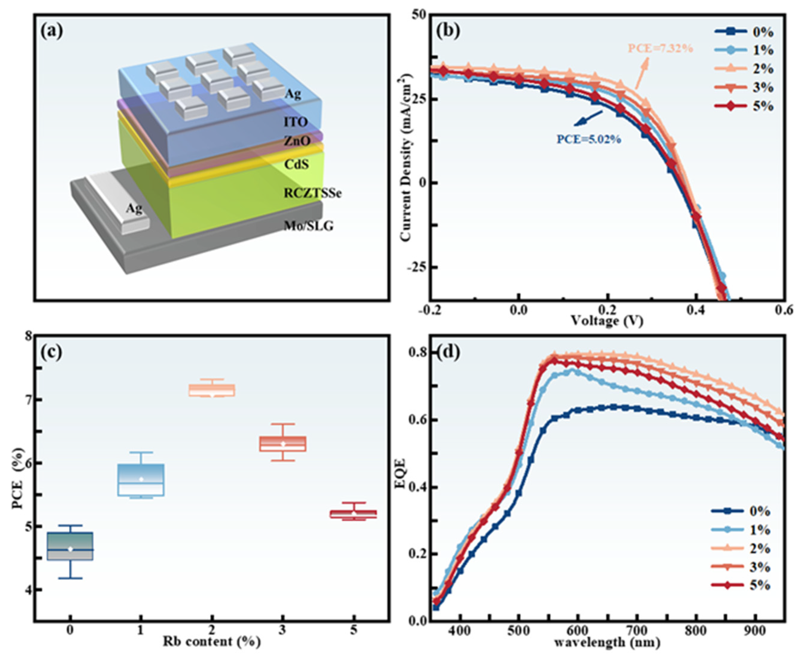
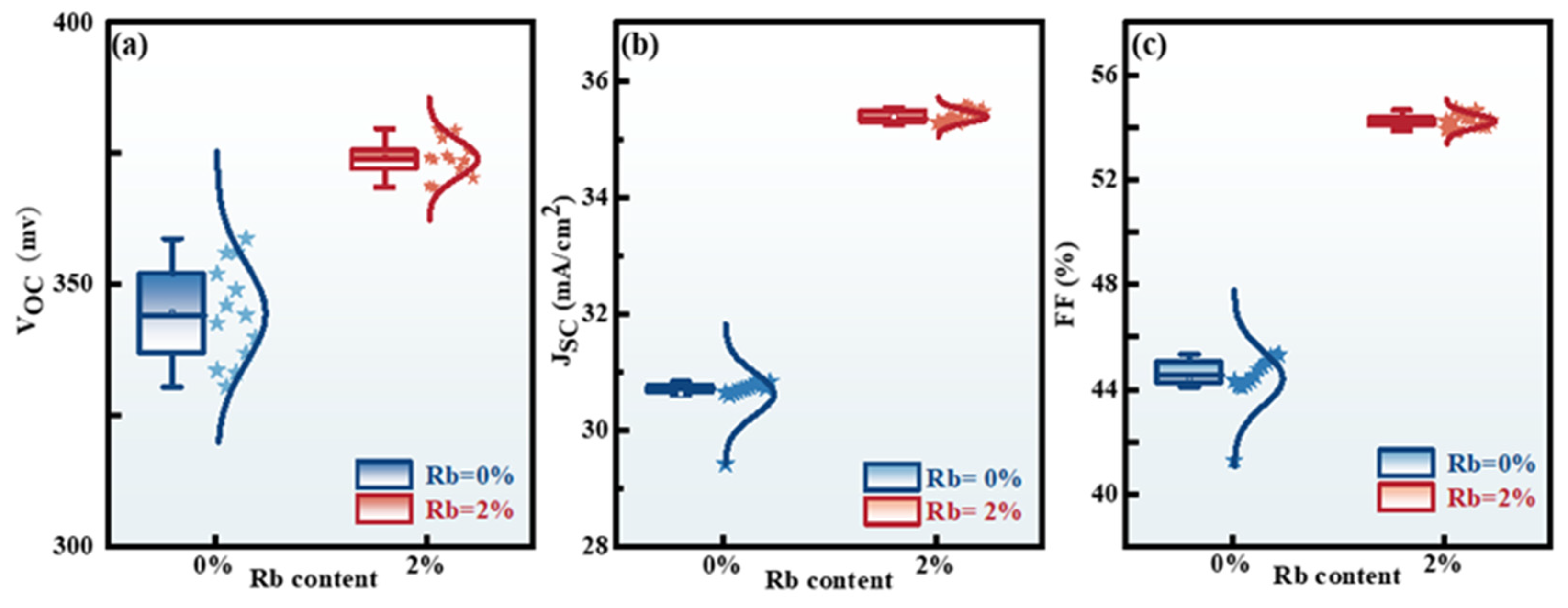
2.3. Device Characterization

To understand the influence of Rb doping on the performance of CZTSSe solar cells, devices with a Ag/ITO/i-ZnO/CdS/RCZTSSe/Mo/SLG structure were prepared, as shown in Figure 9a. RCZTSSe solar cells with varying Rb-doping content were adopted for analysis in detail under simulated AM 1.5 sunshine. Figure 9b displays the J–V curves of the five devices, from which their photovoltaic and electrical characteristics were derived, as showed in Table 3. The J–V curve shows that the device with 2% Rb content exhibited superior photovoltaic characteristics. The maximum PCE of 7.32% was attained by the champion photovoltaic device. Table 3 indicates that, compared to those of the CZTSSe device, the Voc, Jsc, and fill factor (FF) of all RCZTSSe solar cells showed substantial improvements. On the one hand, the increase in Voc might have stemmed from the reduction of CuZn defects and [2CuZn + SnZn] defects from Rb doping, easing the intense band tail states [53]. On the other hand, substituting Cu with Rb might have enabled an adjustment of the valence band edge, causing better alignment of bands between the absorbing and buffer layers, thereby lessening the Voc losses induced by interface mismatch [48,54]. The increase of grain dimensions and crystallinity of the absorbing layer is the reason for the improvement in Jsc and FF [55]. According to Table 3, with an increase in the Rb-doping content from 0% to 5%, the series resistance (Rs) diminished initially, followed by an increase. However, the variation trend of the shunt resistance (Rsh) was contrary to that of Rs. The minimum value of Rs was 12.66 Ω·cm2, and the maximum value of Rsh was 690.58 Ω·cm2 when the content of Rb was 2%. We know that diminishing the number of holes in the RCTSSe absorption layer and an improvement of film smoothness have a positive impact on the RCTSSe/CdS interface, which can suppress the recombination of photogenerated carriers, thereby lessening Rs [56]. Moreover, the increased Rsh was due to CuZn and [2CuZn + SnZn] defects being suppressed by Rb doping and inhibited shunt effect. Therefore, the changes in Rs and Rsh contributed to the further optimization of Jsc and FF.
To guarantee the precision of the experiment, 15 cells were chosen for statistical analysis at each Rb-doping content. The PCE characteristics of solar cells with variable Rb-doping content were assessed using the box diagram (Figure 9c). It was also evident that the PCE of the device was enhanced after Rb doping. In the case of ideal Rb-doping content (i.e., the content of Rb was 2%), the PCE of the RCZTSSe device exhibited the highest efficiency.
The corresponding EQE curves for RCZTSSe solar cells with various Rb contents are shown in Figure 9d. Compare with the un-doped CZTSSe device, the RCZTSSe device exhibited higher optical response throughout the wavelength region, which could be attributed to the reduction of non-radiative recombination [57]. Additionally, Rb doping can also efficiently suppress the formation of the detrimental CuZn defects and related defect clusters, and decrease the route of carrier complexes, thereby enhancing the EQE [58]. A flat and high photoelectric response of nearly 80% was observed for the Rb-2% device within the regions of visible and near-infrared spectra, which indicated that the majority of the deficit induced by the conversion of incident photons into carriers was dealt with, thus enhancing the collection ability of the carriers [59]. It was conducive to the improvement of Jsc. Based on the EQE results, the RCZTSSe thin-film solar cells exhibited enhanced carrier collection abilities compared to those of the un-doped solar cells.
To verify the enhancement of photovoltaic performance, the statistical distributions of other performance characteristics for the Rb-2% and Rb-0% CZTSSe devices were collected and are shown inFigure 10. It was found that the mean values of Voc, Jsc, and FF of the Rb-2% devices were much larger than those of the Rb-0% devices. The increase in Voc could be ascribed to the inhibition of various copper-related defects in the RCZTSSe films, thereby mitigating the detrimental effects of band tail states. The enhancement of Jsc was a result of improved light absorption capabilities. The increase in FF primarily stemmed from the advantageous influence of optimal Rb-doping content on the surface quality of the RCZTSSe films. The outcomes showed that Rb-doped devices significantly outperformed un-doped devices.

3. Experimental Methods

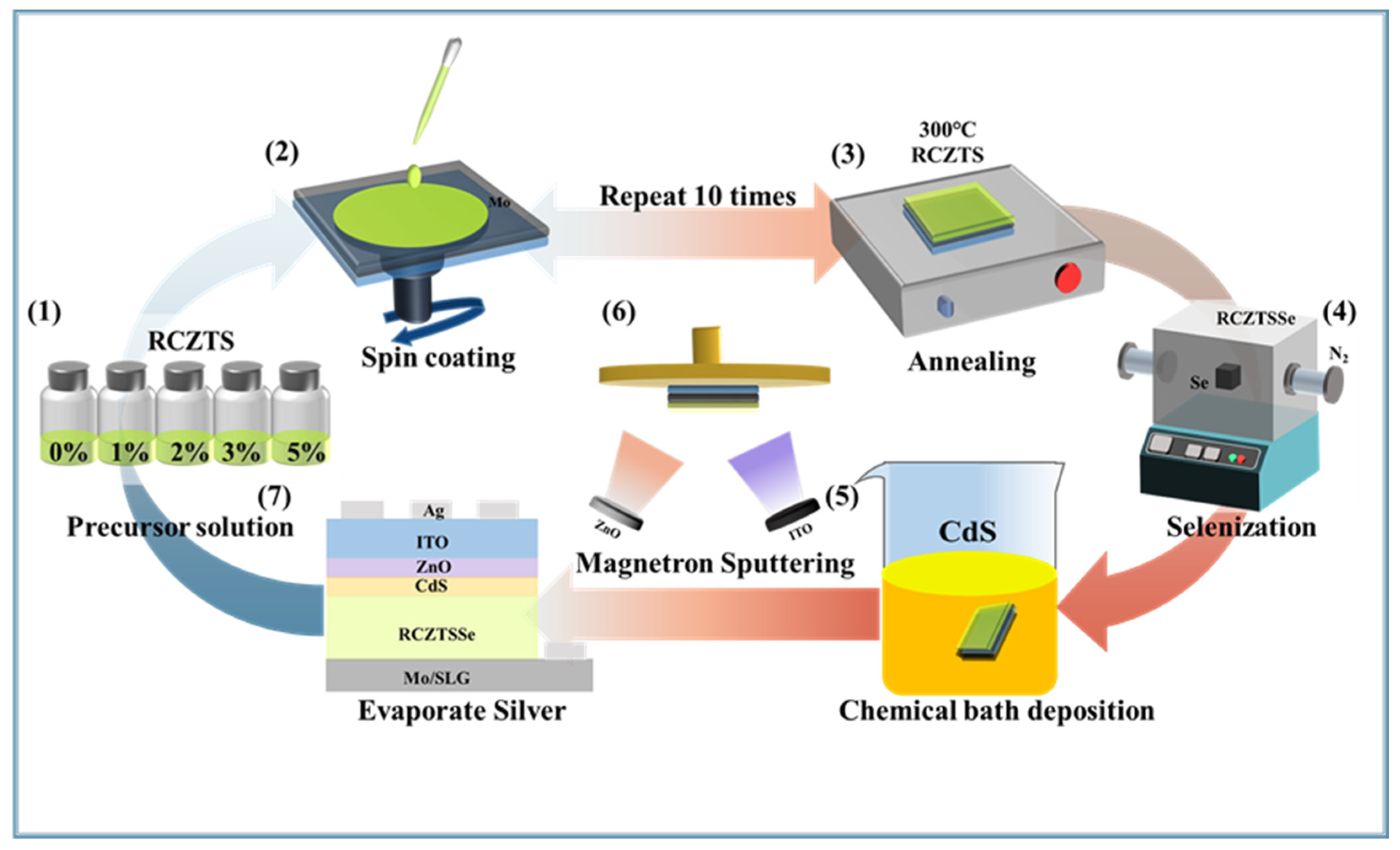
3.1. Preparation of RCZTSSe Thin Films

Firstly, Rb-doped Cu2ZnSnS4 (RCZTS) thin films were synthesized using the sol–gel technique. Appropriate amounts of C4H6CuO4·H2O, ZnCl2, SnCl2·2H2O, CH4N2S, and RbCl were added to DMSO solvent, and C2H7NO was added as a stabilizer. The solution underwent magnetic stirring for a duration of 4 h until the chemicals were all dissolved and the liquid was transparent and clarified. The Rb-doping content in the precursor solution was adjusted by altering the proportion of Rb/(Cu + Rb). The mole ratios of Rb/(Cu + Rb) were set to 0%, 1%, 2%, 3%, and 5%, and the precursor solutions with different Rb-doping contents were obtained. Then, Rb-doped CZTS (RCZTS) precursor films were prepared on 2 × 2 cm2 soda lime glass (SLG) by the spin coating technique. Next, 0.2 g selenium particles and RCZTS film samples were placed in a chamber made of graphite, heated rapidly to 540 °C in two steps in a N2 atmosphere, annealed at this temperature for 15 min, and finally cooled to room temperature to obtain the RCZTSSe films, as shown in Figure 11a. The absorption layer was approximately 1.0 μm thick. The crystal structure of the RCZTSSe thin film is depicted in Figure 11b.

3.2. Solar Cell Fabrication

The RCZTSSe device was prepared using an SLG/Mo/R CZTSSe/CdS/i-ZnO/ITO/Ag structure. As shown in Figure 12, firstly, we introduced a RbCl solution as a Rb source into the precursor solution. The filtered liquid was spin-coated onto Mo-coated SLG operating at 3000 rotations per minute for 30 s, subsequently baked at a temperature of 300 °C on a heated plate to prepare the precursor films. Subsequently, selenium annealing was carried out in a N2 atmosphere. A 60 nm-thick CdS buffer layer was deposited at 65 °C via the standard chemical bath deposition (CBD) process, then, a 60 nm i-ZnO layer and a 250 nm ITO layer were fabricated using magnetron sputtering. Finally, a 200 nm-thick silver electrode was prepared using the thermal evaporation technique. The RCZTSSe device was mechanically divided, and the active area of the measuring device was 0.19 cm2.

3.3. Material and Device Characterization

An X-ray diffractometer (XRD) of Rigaku Company (Rigaku, Tokyo, Japan) was used to explore the crystalline structure of the RCZTSSe thin films. Raman spectra were tracked using a Renishaw spectrometer (Renishaw, London, UK) operating at a specific excitation wavelength of 514 nm. We utilized field emission scanning electron microscopy (FE-SEM, JEOL, Tokyo, Japan) measurements to examine the surface structure of the CZTSSe films. Chemical valence states of Cu, Zn, Sn, S, Se, and Rb were ascertained utilizing X-ray photoelectron spectroscopy (XPS, VG Scienta, Eastgreenstead, East Sussex, UK). The optical bandgap of the samples was evaluated using a UV–Vis spectrophotometer (Shimadzu, Kyoto, Japan). Their electrical characteristics were evaluated using Hall measuring equipment. In this study, we used the Lakeshore 7600 Hall Effect Test System (Lakeshore, Columbus, OH, USA), manufactured in the United States, for testing. The Hall mobility, carrier concentration, and resistivity of the RCZTSSe samples were measured using the four-probe Hall effect measurement method. The current–voltage (J–V) data of the solar cells were fetched by simulating daylight with AM 1.5G illumination. External quantum efficiency (EQE) was obtained by measuring the solar cells with a Zolix Solar Cell Scan100 instrument (Zolix, Beijing, China).

4. Conclusions

In conclusion, Rb cations were introduced by adding a RbCl solution into a CZTS precursor solution. Rb cation-doped CZTSSe thin films were synthesized using the sol–gel method accompanied by the post-selenization technique for the first time. A systematic investigation showed that an appropriate amount of Rb doping greatly improved the crystallinity of CZTSSe thin films, enhanced the surface morphology, and accelerated the growth of grains. When the content of Rb was 2%, the average size of the grain of the film was maximal. As the doping content of Rb increased, the Eg of RCZSSe thin films gradually increased. Hall measurement showed that the Rb-2% RCZTSSe film had the best electrical performance. Our comprehensive research indicates that Rb doping can significantly decrease the defect density of CuZn and [2CuZn + SnZn] defects, thereby improving the light absorption and enhancing charge transport. Finally, on account of the enhanced absorber quality, kinetics of carrier transport, and defect characteristics, Rb-2% was capable of substantial improvements in Voc and Jsc concurrently, resulting in an efficiency boost from 5.02% to 7.32%. Overall, this work demonstrates the optimistic function of Rb doping in inhibiting the various copper-related defects and provides more hopeful possibilities for the progress of alkali metal-doped CZTSSe photovoltaic devices.

Author Contributions

Conceptualization, B.Y.; Methodology, C.M.; Software, Y.C.; Validation, Y.S. and L.Y.; Formal analysis, Y.C. and X.L.; Investigation, Z.W. and F.W.; Resources, X.L.; Writing—original draft, C.M.; Writing—review & editing, Y.S. and B.Y.; Visualization, L.Y.; Supervision, F.W. All authors have read and agreed to the published version of the manuscript.

Funding

This research was funded by the Program for the development of Science and Technology of Jilin province Grant Nos. 20210101410JC, 20220101004JC; National Natural Science Foundation of China under Grant Nos. 62274077.

Institutional Review Board Statement

Not applicable.

Informed Consent Statement

Informed consent was obtained from all subjects involved in the study.

Data Availability Statement

The authors do not have permission to share data.

Conflicts of Interest

The authors declare no conflict of interest.

References

  1. Zhou, H.; Hsu, W.-C.; Duan, H.-S.; Bob, B.; Yang, W.; Song, T.-B.; Hsu, C.-J.; Yang, Y. CZTS nanocrystals: A promising approach for next generation thin film photovoltaics. Energy Environ. Sci. 2013, 6, 2822–2838. [Google Scholar] [CrossRef]
  2. Xie, W.; Yan, Q.; Sun, Q.; Li, Y.; Zhang, C.; Deng, H.; Cheng, S. A Progress Review on Challenges and Strategies of Flexible Cu2ZnSn(S, Se)4 Solar Cells. Solar RRL 2023, 7, 2201036. [Google Scholar] [CrossRef]
  3. Li, J.; Sun, K.; Yuan, X.; Huang, J.; Green, M.A.; Hao, X. Emergence of flexible kesterite solar cells: Progress and perspectives. npj Flexible Electron. 2023, 7, 16. [Google Scholar] [CrossRef]
  4. Wang, D.; Zhao, W.; Zhang, Y.; Liu, S. Path towards high-efficient kesterite solar cells. J. Energy Chem. 2018, 27, 1040–1053. [Google Scholar] [CrossRef]
  5. Li, W.; Tan, J.M.R.; Leow, S.W.; Lie, S.; Magdassi, S.; Wong, L.H. Recent Progress in Solution-Processed Copper-Chalcogenide Thin-Film Solar Cells. Energy Technol. 2018, 6, 46–59. [Google Scholar] [CrossRef]
  6. Shockley, W.; Queisser, H.J. Detailed Balance Limit of Efficiency of p-n Junction Solar Cells. J. Appl. Phys. 1961, 32, 510–519. [Google Scholar] [CrossRef]
  7. Li, Y.; Cui, C.; Wei, H.; Shao, Z.; Wu, Z.; Zhang, S.; Wang, X.; Pang, S.; Cui, G. Suppressing Element Inhomogeneity Enables 14.9% Efficiency CZTSSe Solar Cells. Adv. Mater. 2024, 36, 2400138. [Google Scholar] [CrossRef] [PubMed]
  8. Luo, Z.; Yu, L.; Zheng, T.; Dong, X.; Yang, F.; Chen, J.; Zhang, X.; Zhao, Y.; Li, Y. Promoting effect of lanthanum doping on photovoltaic performance of CZTSSe solar cells. J. Chem. Phys. 2024, 160, 164712. [Google Scholar] [CrossRef] [PubMed]
  9. Moore, J.E.; Hages, C.J.; Agrawal, R.; Lundstrom, M.S.; Gray, J.L. The importance of band tail recombination on current collection and open-circuit voltage in CZTSSe solar cells. Appl. Phys. Lett. 2016, 109, 021102. [Google Scholar] [CrossRef]
  10. Nisika; Kaur, K.; Kumar, M. Progress and prospects of CZTSSe/CdS interface engineering to combat high open-circuit voltage deficit of kesterite photovoltaics: A critical review. J. Mater. Chem. A 2020, 8, 21547–21584. [Google Scholar] [CrossRef]
  11. Kangsabanik, M.; Gayen, R.N. A Comprehensive Review on the Recent Strategy of Cation Substitution in CZTS(Se) Thin Films to Achieve Highly Efficient Kesterite Solar Cells. Solar RRL 2023, 7, 2300670. [Google Scholar] [CrossRef]
  12. Yuan, Z.-K.; Chen, S.; Xiang, H.; Gong, X.-G.; Walsh, A.; Park, J.-S.; Repins, I.; Wei, S.-H. Engineering Solar Cell Absorbers by Exploring the Band Alignment and Defect Disparity: The Case of Cu- and Ag-Based Kesterite Compounds. Adv. Funct. Mater. 2015, 25, 6733–6743. [Google Scholar] [CrossRef]
  13. Gokmen, T.; Gunawan, O.; Todorov, T.K.; Mitzi, D.B. Band tailing and efficiency limitation in kesterite solar cells. Appl. Phys. Lett. 2013, 103, 103506. [Google Scholar] [CrossRef]
  14. Yu, X.; Cheng, S.; Yan, Q.; Fu, J.; Jia, H.; Sun, Q.; Yang, Z.; Wu, S. Efficient flexible Mo foil-based Cu2ZnSn(S, Se)4 solar cells from In-doping technique. Sol. Energy Mater. Sol. Cells 2020, 209, 110434. [Google Scholar] [CrossRef]
  15. Ren, G.; Zhuang, D.; Zhao, M.; Wei, Y.; Wu, Y.; Li, X.; Lyu, X.; Wang, C.; Li, Y. Cu2ZnSn(S, Se)4 solar cell with slight band tailing states achieves 11.83% efficiency by selenizing sputtered Cu–Zn–Sn–S precursor. J. Power Sources 2020, 479, 228747. [Google Scholar] [CrossRef]
  16. Wei, H.; Li, Y.; Cui, C.; Wang, X.; Shao, Z.; Pang, S.; Cui, G. Defect suppression for high-efficiency kesterite CZTSSe solar cells: Advances and prospects. Chem. Eng. J. 2023, 462, 142121. [Google Scholar] [CrossRef]
  17. Li, J.; Wang, D.; Li, X.; Zeng, Y.; Zhang, Y. Cation Substitution in Earth-Abundant Kesterite Photovoltaic Materials. Adv. Sci. 2018, 5, 1700744. [Google Scholar] [CrossRef] [PubMed]
  18. Dhawale, D.S.; Ali, A.; Lokhande, A.C. Impact of various dopant elements on the properties of kesterite compounds for solar cell applications: A status review. Sustain. Energy Fuels 2019, 3, 1365–1383. [Google Scholar] [CrossRef]
  19. Cabas-Vidani, A.; Haass, S.G.; Andres, C.; Caballero, R.; Figi, R.; Schreiner, C.; Márquez, J.A.; Hages, C.; Unold, T.; Bleiner, D.; et al. High-Efficiency (LixCu1−x)2ZnSn(S,Se)4 Kesterite Solar Cells with Lithium Alloying. Adv. Energy Mater. 2018, 8, 1801191. [Google Scholar] [CrossRef]
  20. Yang, W.; Ji, Y.; Chen, W.; Pan, Y.; Chen, Z.; Wu, S.; Russo, S.P.; Xu, Y.; Smith, T.A.; Chesman, A.; et al. The Multiple Roles of Na Ions in Highly Efficient CZTSSe Solar Cells. Small 2024, 20, 2307807. [Google Scholar] [CrossRef] [PubMed]
  21. Dong, L.; Tao, S.; Zhao, M.; Zhuang, D.; Wang, Y.; Wang, H.; Jia, M.; Han, J.; Zhu, H. Crystallization mechanism and defect passivation of Cu2ZnSn(S,Se)4 thin film solar cells via in situ potassium doping. J. Mater. Chem. A 2023, 11, 20139–20150. [Google Scholar] [CrossRef]
  22. Jackson, P.; Wuerz, R.; Hariskos, D.; Lotter, E.; Witte, W.; Powalla, M. Effects of heavy alkali elements in Cu(In,Ga)Se2 solar cells with efficiencies up to 22.6%. Phys. Status. Solidi-R 2016, 10, 583–586. [Google Scholar] [CrossRef]
  23. Ishizuka, S.; Taguchi, N.; Fons, P.J. Similarities and Critical Differences in Heavy Alkali-Metal Rubidium and Cesium Effects on Chalcopyrite Cu(In,Ga)Se2 Thin-Film Solar Cells. J. Phys. Chem. C 2019, 123, 17757–17764. [Google Scholar] [CrossRef]
  24. Wu, Y.; Zhao, M.; Zhuang, D.; Zhang, N.; Yu, X.; Wei, Y.; Lyu, X.; Ren, G.; Wang, C.; Hu, L.; et al. The effect of Rb doping on CZTSSe solar cells. Sol. Energy 2019, 187, 269–273. [Google Scholar] [CrossRef]
  25. Lee, T.; Hamim Sharif, M.; Enkhbayar, E.; Enkhbat, T.; Salahuddin Mina, M.; Kim, J. Defect Passivation for Kesterite CZTSSe Solar Cells via In Situ Al2O3 Incorporation into the Bulk CZTSSe Absorber. Solar RRL 2022, 6, 2100862. [Google Scholar] [CrossRef]
  26. Datt, G.; Raja, M.M.; Abhyankar, A.C. Steering of Magnetic Interactions in Ni0.5Zn0.5Fe2–x (Mn)xO4 Nanoferrites via Substitution-Induced Cationic Redistribution. J. Phys. Chem. C 2021, 125, 10693–10707. [Google Scholar] [CrossRef]
  27. Zhuk, S.; Wong, T.K.S.; Hadke, S.S.; Lie, S.; Guchhait, A.; Gao, Y.; Wong, L.H.; Cheng, S.; Wang, X.; Dalapati, G.K. Molybdenum incorporated Cu1. 69ZnSnS4 kesterite photovoltaic devices with bilayer microstructure and tunable optical-electronic properties. Sol. Energy Mater. Sol. Cells 2019, 194, 777–787. [Google Scholar]
  28. Mondal, R.; Chandra, G.H.; Subbaiah, Y.P.V.; Gupta, M.; Prasada Rao, R. Insights into the structural and optical properties of (Cu,Ag)2ZnSnSe4 thin films: Role of pre-annealing and selenization times. Opt. Mater. 2024, 154, 115618. [Google Scholar] [CrossRef]
  29. Farooq, U.; Ali Shah, U.; Ishaq, M.; Hu, J.-G.; Ahmed, S.; Chen, S.; Zheng, Z.-H.; Su, Z.-H.; Fan, P.; Liang, G.-X. Defects passivation by solution-processed titanium doping strategy towards high efficiency kesterite solar cells. Chem. Eng. J. 2023, 451, 139109. [Google Scholar] [CrossRef]
  30. Qi, Y.-F.; Kou, D.-X.; Zhou, W.-H.; Zhou, Z.-J.; Tian, Q.-W.; Meng, Y.-N.; Liu, X.-S.; Du, Z.-L.; Wu, S.-X. Engineering of interface band bending and defects elimination via a Ag-graded active layer for efficient (Cu,Ag)2ZnSn(S,Se)4 solar cells. Energy Environ. Sci. 2017, 10, 2401–2410. [Google Scholar] [CrossRef]
  31. Cui, C.; Fu, J.; Kou, D.; Li, Y.; Wei, H.; Wu, Z.; Zhou, W.; Zhou, Z.; Yuan, S.; Qi, Y.; et al. Heterojunction reconstruction via In doping towards high-efficiency CZTSSe solar cells. Chem. Eng. J. 2023, 476, 146701. [Google Scholar] [CrossRef]
  32. Du, Y.; Tian, Q.; Huang, J.; Zhao, Y.; Chang, X.; Zhang, A.; Wu, S. Heterovalent Ga3+ doping in solution-processed Cu 2 ZnSn (S, Se) 4 solar cells for better optoelectronic performance. Sustainable Energy Fuels 2020, 4, 1621–1629. [Google Scholar] [CrossRef]
  33. Danilson, M.; Altosaar, M.; Kauk, M.; Katerski, A.; Krustok, J.; Raudoja, J. XPS study of CZTSSe monograin powders. Thin Solid Films 2011, 519, 7407–7411. [Google Scholar] [CrossRef]
  34. Tsega, M.; Dejene, F.B.; Kuo, D.-H. Morphological evolution and structural properties of Cu2ZnSn(S,Se)4 thin films deposited from single ceramic target by a one-step sputtering process and selenization without H2Se. J. Alloys Compd. 2015, 642, 140–147. [Google Scholar] [CrossRef]
  35. Fu, J.; Tian, Q.; Zhou, Z.; Kou, D.; Meng, Y.; Zhou, W.; Wu, S. Improving the performance of solution-processed Cu2ZnSn(S, Se)4 photovoltaic materials by Cd2+ substitution. Chem. Mater. 2016, 28, 5821–5828. [Google Scholar] [CrossRef]
  36. Zhao, J.; Liang, G.-X.; Hu, J.-G.; Zheng, Z.-H.; Luo, J.-T.; Zhang, D.-P.; Zeng, Y.; Fan, P. Substrate Temperature-Assisted Preparation of CZTSSe Thin Films by a Single Quinary Target. J. Electron. Mater. 2018, 47, 873–878. [Google Scholar] [CrossRef]
  37. Maticiuc, N.; Kodalle, T.; Lauche, J.; Wenisch, R.; Bertram, T.; Kaufmann, C.A.; Lauermann, I. In vacuo XPS investigation of Cu(In,Ga)Se2 surface after RbF post-deposition treatment. Thin Solid Films 2018, 665, 143–147. [Google Scholar] [CrossRef]
  38. Chander, S.; Dhaka, M.S. CdCl2 treatment concentration evolution of physical properties correlation with surface morphology of CdTe thin films for solar cells. Mater. Res. Bull. 2018, 97, 128–135. [Google Scholar] [CrossRef]
  39. Datt, G.; Abhyankar, A. Dopant driven tunability of dielectric relaxation in MxCo(1-x)Fe2O4 (M: Zn2+, Mn2+, Ni2+) nano-ferrites. J. Appl. Phys. 2017, 122, 034102. [Google Scholar] [CrossRef]
  40. Hsieh, Y.-T.; Han, Q.; Jiang, C.; Song, T.-B.; Chen, H.; Meng, L.; Zhou, H.; Yang, Y. Efficiency Enhancement of Cu2ZnSn(S,Se)4 Solar Cells via Alkali Metals Doping. Adv. Energy Mater. 2016, 6, 1502386. [Google Scholar] [CrossRef]
  41. Zhou, J.; Xu, X.; Duan, B.; Wu, H.; Shi, J.; Luo, Y.; Li, D.; Meng, Q. Regulating crystal growth via organic lithium salt additive for efficient Kesterite solar cells. Nano Energy 2021, 89, 106405. [Google Scholar] [CrossRef]
  42. Zeng, C.; Liang, Y.; Zeng, L.; Zhang, L.; Zhou, J.; Huang, P.; Hong, R. Effect of S/(S + Se) ratio during the annealing process on the performance of Cu2ZnSn(S, Se)4 solar cells prepared by sputtering from a quaternary target. Sol. Energy Mater. Sol. Cells 2019, 203, 110167. [Google Scholar] [CrossRef]
  43. Yu, Q.; Shi, J.; Guo, L.; Duan, B.; Luo, Y.; Wu, H.; Li, D.; Meng, Q. Eliminating multi-layer crystallization of Cu2ZnSn(S, Se)4 absorber by controlling back interface reaction. Nano Energy 2020, 76, 105042. [Google Scholar] [CrossRef]
  44. Tlili, M.; Jebbari, N.; Naffouti, W.; Kamoun, N.T. Effect of precursor nature on physical properties of chemically sprayed MgO thin films for optoelectronic application. Eur. Phys. J. Plus 2020, 135, 687. [Google Scholar] [CrossRef]
  45. Khadka, D.B.; Kim, J. Structural transition and band gap tuning of Cu2(Zn, Fe)SnS4 chalcogenide for photovoltaic application. J. Phys. Chem. C 2014, 118, 14227–14237. [Google Scholar] [CrossRef]
  46. Qi, Y.; Tian, Q.; Meng, Y.; Kou, D.; Zhou, Z.; Zhou, W.; Wu, S. Elemental Precursor Solution Processed (Cu1–xAgx)2ZnSn(S, Se)4 Photovoltaic Devices with over 10% Efficiency. ACS Appl. Mater. Interfaces 2017, 9, 21243–21250. [Google Scholar] [CrossRef]
  47. Zhang, Y.; Sun, X.; Zhang, P.; Yuan, X.; Huang, F.; Zhang, W. Structural properties and quasiparticle band structures of Cu-based quaternary semiconductors for photovoltaic applications. J. Appl. Phys. 2012, 111, 063709. [Google Scholar] [CrossRef]
  48. Chen, S.; Walsh, A.; Luo, Y.; Yang, J.-H.; Gong, X.; Wei, S.-H. Wurtzite-derived polytypes of kesterite and stannite quaternary chalcogenide semiconductors. Phys. Rev. B 2010, 82, 195203. [Google Scholar] [CrossRef]
  49. Li, Y.; Wei, H.; Cui, C.; Wang, X.; Shao, Z.; Pang, S.; Cui, G. CZTSSe solar cells: Insights into interface engineering. J. Mater. Chem. A 2023, 11, 4836–4849. [Google Scholar] [CrossRef]
  50. Maurya, K.; Singh, V. Sb2Se3/CZTS dual absorber layer based solar cell with 36.32% efficiency: A numerical simulation. J. Sci. Adv. Mater. Devices 2022, 7, 100445. [Google Scholar]
  51. Son, D.-H.; Kim, Y.-I.; Kim, S.-H.; Nam, D.; Cheong, H.; Kang, J.-K.; Yang, K.-J.; Kim, D.-H. Effects of S and Se contents on the physical and photovoltaic properties of Cu2ZnSn(SX, Se1−X)4 thin films: Achieving a PCE of 9.47%. J. Mater. Chem. A 2019, 7, 22986–22995. [Google Scholar] [CrossRef]
  52. Du, Y.; Wang, S.; Tian, Q.; Zhao, Y.; Chang, X.; Xiao, H.; Deng, Y.; Chen, S.; Wu, S.; Liu, S. Defect Engineering in Earth-Abundant Cu2ZnSn(S,Se)4 Photovoltaic Materials via Ga3+-Doping for over 12% Efficient Solar Cells. Adv. Funct. Mater. 2021, 31, 2010325. [Google Scholar] [CrossRef]
  53. Andrade-Arvizu, J.; Fonoll-Rubio, R.; Sánchez, Y.; Becerril-Romero, I.; Malerba, C.; Valentini, M.; Calvo-Barrio, L.; Izquierdo-Roca, V.; Placidi, M.; Vigil-Galán, O. Rear band gap grading strategies on Sn–Ge-alloyed kesterite solar cells. J. Alloys Compd. 2020, 3, 10362–10375. [Google Scholar] [CrossRef]
  54. Ahmad, F.; Lakhtakia, A.; Anderson, T.H.; Monk, P.B. Towards highly efficient thin-film solar cells with a graded-bandgap CZTSSe layer. J. Phys. Energy 2020, 2, 025004. [Google Scholar] [CrossRef]
  55. Cao, Y.; Liu, C.; Yang, T.; Zhao, Y.; Na, Y.; Jiang, C.; Zhou, J.; Pang, J.; Liu, H.; Rummeli, M.H. Gradient bandgap modification for highly efficient carrier transport in antimony sulfide-selenide tandem solar cells. Sol. Energy Mater. Sol. Cells 2022, 246, 111926. [Google Scholar] [CrossRef]
  56. Meng, L.; Yao, B.; Li, Y.; Ding, Z.; Xiao, Z.; Liu, K.; Wang, G. Significantly enhancing back contact adhesion and improving stability of Cu2(Zn, Cd)Sn(S, Se)4 solar cell by a rational carbon doping strategy. J. Alloys Compd. 2017, 710, 403–408. [Google Scholar] [CrossRef]
  57. Mattheis, J.; Rostan, P.; Rau, U.; Werner, J. Carrier collection in Cu(In, Ga)Se2 solar cells with graded band gaps and transparent ZnO: Al back contacts. Sol. Energy Mater. Sol. Cells 2007, 91, 689–695. [Google Scholar] [CrossRef]
  58. Wu, Y.; Sui, Y.; He, W.; Zeng, F.; Wang, Z.; Wang, F.; Yao, B.; Yang, L. Substitution of Ag for Cu in Cu2ZnSn(S, Se)4: Toward wide band gap absorbers with low antisite defects for thin film solar cells. Nano Mater. 2020, 10, 96. [Google Scholar] [CrossRef] [PubMed]
  59. Chen, X.-Y.; Ishaq, M.; Ahmad, N.; Tang, R.; Zheng, Z.-H.; Hu, J.-G.; Su, Z.-H.; Fan, P.; Liang, G.-X.; Chen, S. Ag, Ti dual-cation substitution in Cu2ZnSn(S, Se)4 induced growth promotion and defect suppression for high-efficiency solar cells. J. Mater. Chem. A 2022, 10, 22791–22802. [Google Scholar] [CrossRef]
Figure 1. (a) XRD spectra of RCZTSSe thin films with various Rb contents of 0%, 1%, 2%, 3%, and 5%. (b) Enlarged image of the (112) diffraction peaks.
Molecules 29 03670 g001
Figure 2. Variation trend in 2θ, FWHM, and intensity of (112) peaks with various Rb-doping contents of RCZTSSe films.
Molecules 29 03670 g002
Figure 3. (a) Lattice constants a and c of the RCZTSSe thin films with different Rb contents of 0%, 1%, 2%, 3%, and 5%. (b) ƞ and V of the RCZTSSe thin films with various Rb-doping contents.
Molecules 29 03670 g003
Figure 4. (a) Raman spectra of the RCZTSSe thin films with different Rb-doping contents, and enlarged Raman spectra of the Rb-0% and Rb-2% RCZTSSe thin films in the range of 210–255 cm−1. (b) The variation tendency chart of the primary Raman peaks of the A1 mode with different Rb-doping contents.
Molecules 29 03670 g004
Figure 5. XPS spectra of (a) Cu 2p, (b) Zn 2p, (c) Sn 3d, (d) S 2p, (e) Se 3d, and (f) Rb 3d of the RCZTSSe 0thin film.
Molecules 29 03670 g005
Figure 6. SEM images of RCZTSSe films with various Rb contents: (a) Rb-0%, (b) Rb-1%, (c) Rb-2%, (d) Rb-2%, and (e) Rb-5%. (f) The average grain dimensions in the films. EDS mapping images of Cu, Zn, Sn, S, Se, and Rb elements in the Rb-2% thin film.
Molecules 29 03670 g006
Figure 7. (a) Atomic percentage of all elements in RCZTSSe films with different Rb contents. (b) Ratio of elemental composition of Rb and Cu in RCZTSSe films with different Rb contents.
Molecules 29 03670 g007
Figure 8. (a) (αhυ)2 versus photon energy (hυ) for the RCZTSSe thin films with diverse Rb contents (Rb-0%, Rb-1%, Rb-2%, Rb-3%, and Rb-5%). (b) Variation trend of bandgaps of the RCZTSSe films with Rb content.
Molecules 29 03670 g008
Figure 9. (a) The diagrammatic configuration of the RCZTSSe solar cell. (b) Optimal J–V curves of RCZTSSe devices with various Rb-doping contents under standard AM 1.5 sunshine. (c) Box diagrams of PCE derived from 15 s olar cells. (d) EQE spectrum of the RCZTSSe solar cells.
Molecules 29 03670 g009
Figure 10. Statistical box diagrams of performance parameters of Rb-0% and Rb-2% devices: (a) Voc, (b) Jsc, and (c) FF.
Molecules 29 03670 g010
Figure 11. (a) Temperature profiles of a two-step selenization process. (b) The crystal structure cell of kesterite RCZTSSe.
Molecules 29 03670 g011
Figure 12. Schematic drawing of the preparation process of an RCZTSSe solar cell. (1) Preparing an RCZTS precursor solution with different Rb-doping content; (2) spin-coating the precursor solution; (3) annealing the RCZTS thin film; (4) selenization in a N2 atmosphere; (5) preparing a CdS layer by chemical bath deposition; (6) preparing ZnO and ITO layers by magnetron sputtering; (7) preparing a silver electrode.
Molecules 29 03670 g012
Table 1. Overview of the EDS findings of RCZTSSe thin films with different Rb-doping contents.
xComposition(%at)Cu + Rb/(Zn + Sn)Rb/(Rb + Cu)
CuZnSnSSeRb
023.96 ± 0.117.15 ± 0.2811.27 ± 0.133.15 ± 0.3944.47 ± 0.9100.84 ± 0.010
0.0123.40 ± 0.0317.71 ± 0.5910.15 ± 0.472.15 ± 0.4945.89 ± 0.440.70 ± 0.130.87 ± 0.010.03
0.0223.26 ± 0.2317.43 ± 0.4510.37 ± 0.451.99 ± 0.5245.77 ± 0.631.18 ± 0.350.880.05 ± 0.01
0.0323.48 ± 0.1617.27 ± 0.119.96 ± 0.292.71 ± 0.5145.23 ± 0.381.35 ± 0.120.91 ± 0.020.05
0.0522.80 ± 0.4516.2 ± 0.7113.18 ± 0.772.35 ± 0.0143.92 ± 0.571.55 ± 0.180.83 ± 0.020.07 ± 0.01
Table 2. Electrical properties of the RCZTSSe thin films.
SamplesResistivity (Ω·cm2)Carrier Concentration (cm−3)Mobility (cm2V−1s−1)Type
Rb = 0%9.966.26 × 10172.23 × 101p
Rb = 1%2.94 × 1012.13 × 10174.83 × 101p
Rb = 2%4.91 × 1011.27 × 10176.64 × 101p
Rb = 3%1.43 × 1014.37 × 10171.60 × 101P
Rb = 5%1.227.28 × 10187.03 × 10−1P
Table 3. The features of RCZTSSe thin-film solar cells with various Rb-doping contents. Overview of device parameters of the RCZTSSe solar cells with various Rb-doping contents.
Device.Active Area (cm2)VOC (mV)JSC (mA/cm−2)FF (%)PCE (%)Rs (Ω·cm2)Rsh(Ω·cm2)
CZTSSe (Rb = 0%)0.19358.75 ± 7.3730.84 ± 0.8145.33 ± 2.175.02 ± 0.4419.36 ± 1.16279.76 ± 28.19
CZTSSe (Rb = 1%)0.19374.73 ± 12.0332.33 ± 2.3550.92 ± 0.726.17 ± 0.3416.84 ± 1.84641.44 ± 66.31
CZTSSe (Rb = 2%)0.19379.69 ± 3.9935.27 ± 0.1654.66 ± 0.317.32 ± 0.1012.66 ± 0.47690.58 ± 21.85
CZTSSe (Rb = 3%)0.19371.03 ± 12.7233.52 ± 3.0753.12 ± 1.026.61 ± 0.6512.87 ± 2.14526.30 ± 44.5
CZTSSe (Rb = 5%)0.19366.11 ± 3.1732.32 ± 0.5945.55 ± 0.135.39 ± 0.1319.78 ± 0.52272.59 ± 4.92
Disclaimer/Publisher’s Note: The statements, opinions and data contained in all publications are solely those of the individual author(s) and contributor(s) and not of MDPI and/or the editor(s). MDPI and/or the editor(s) disclaim responsibility for any injury to people or property resulting from any ideas, methods, instructions or products referred to in the content.

