
Design and Analysis of a Novel 24 GHz Up-Conversion Mixer with Improved Derivative Super-Position Linearizer Technique for 5G Applications

 , , and
Abstract
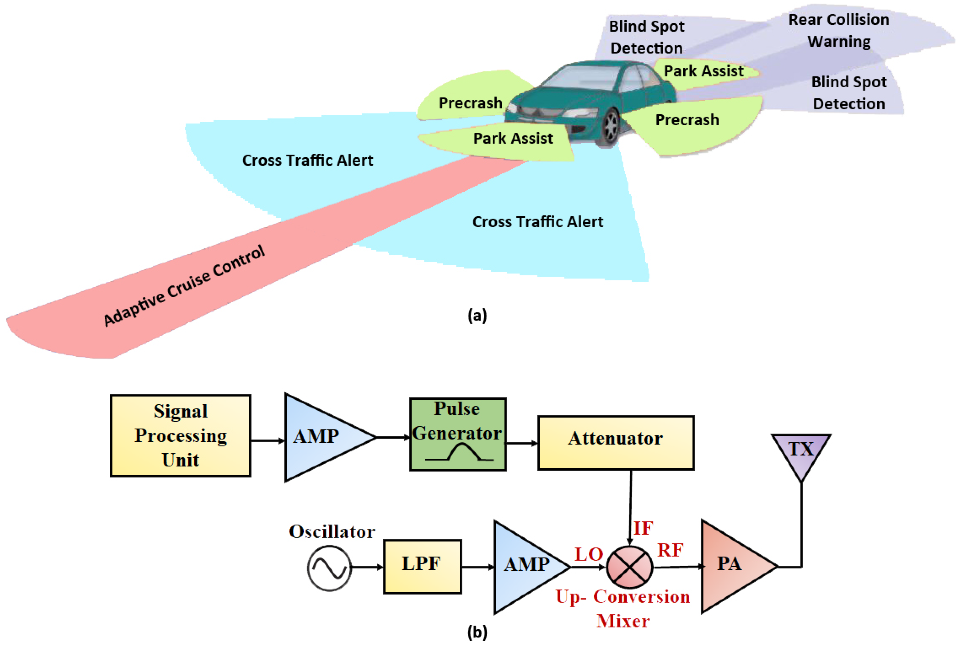
:1. Introduction
Related Literature Survey
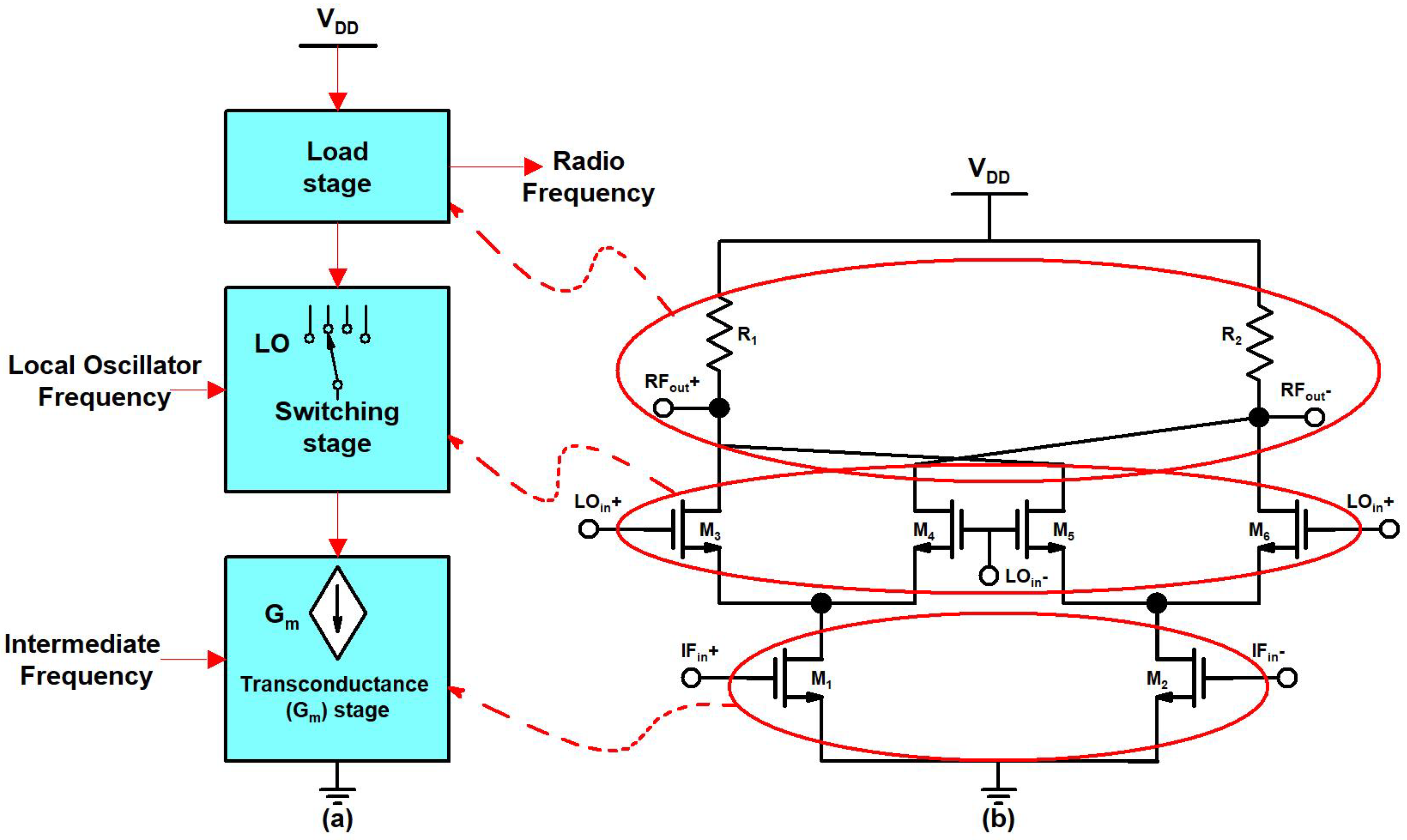
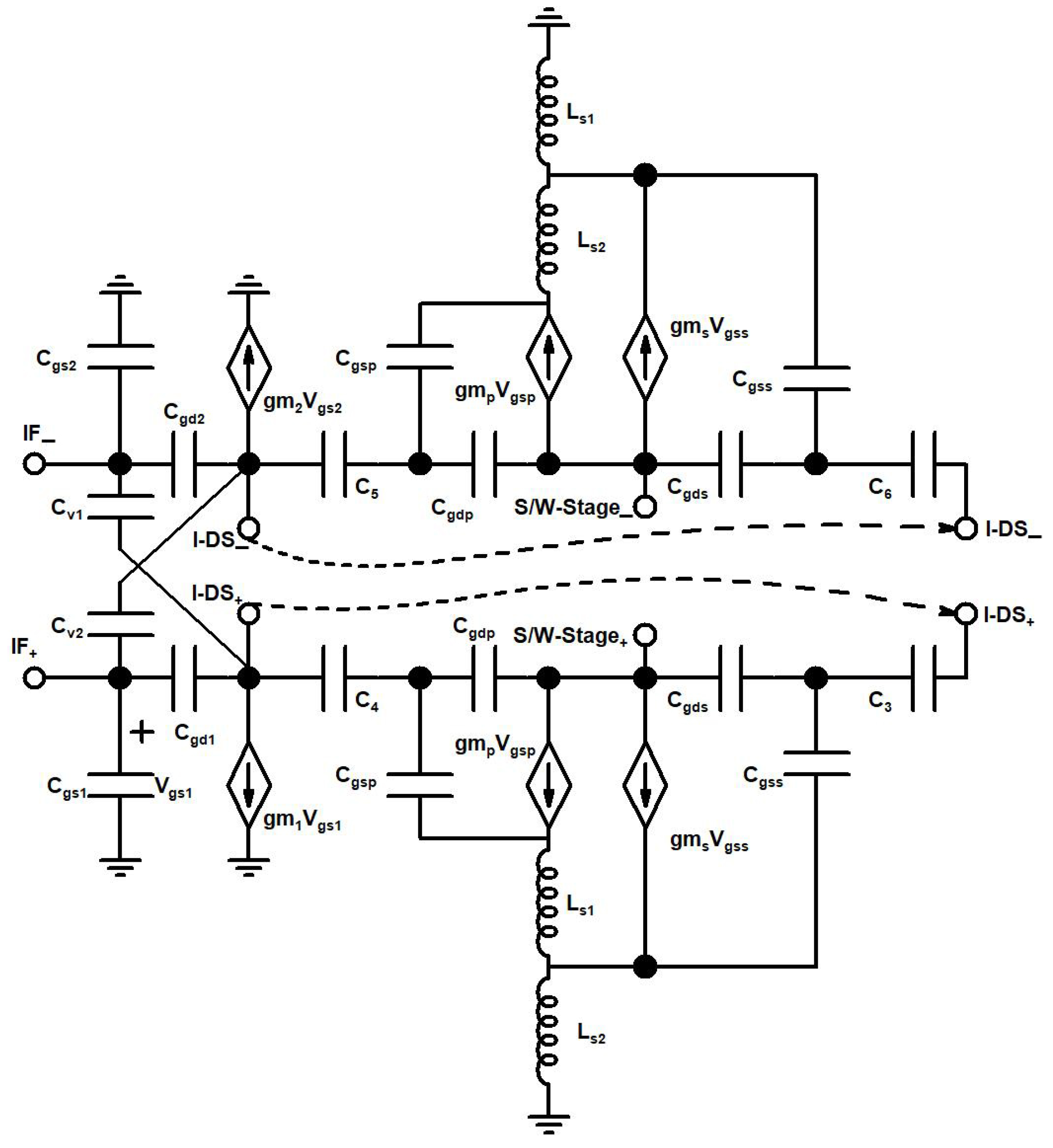
2. Proposed Up-Conversion Mixer Design
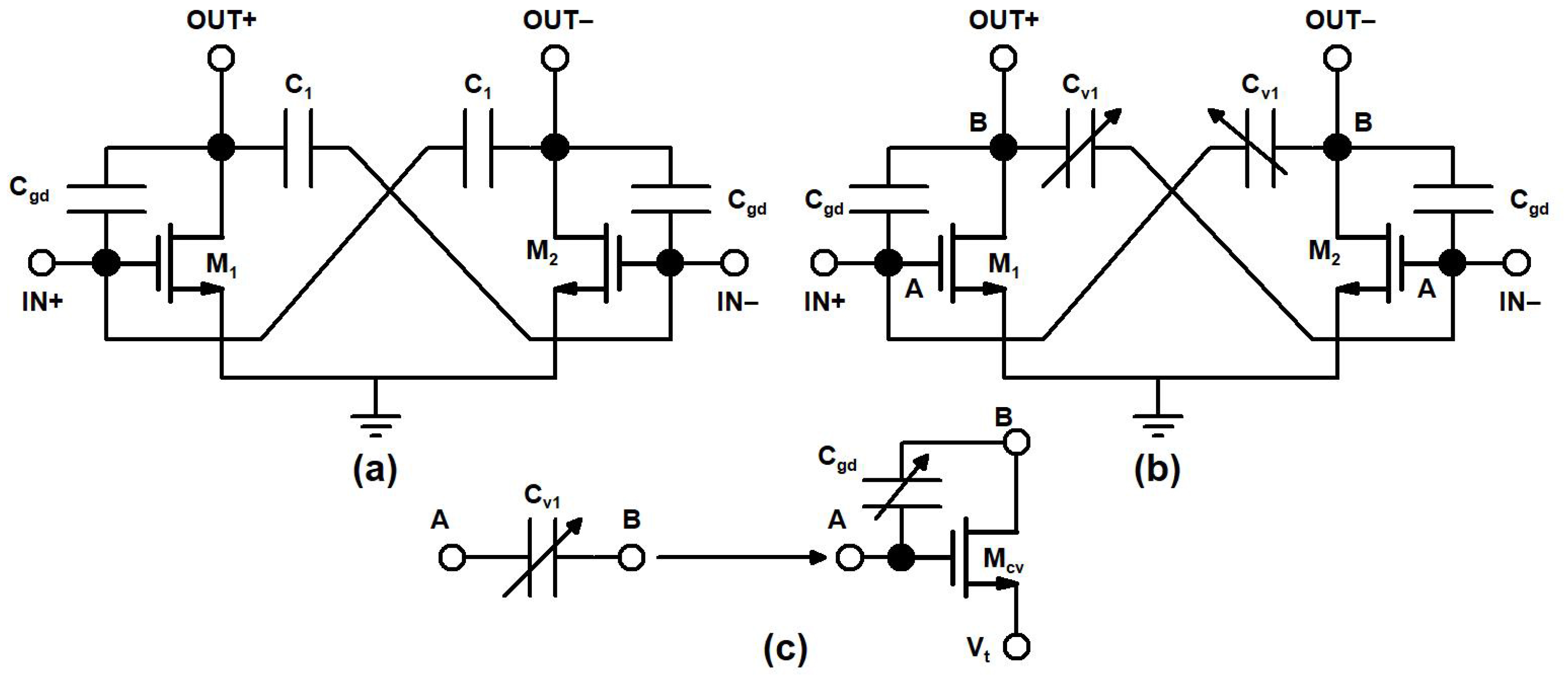
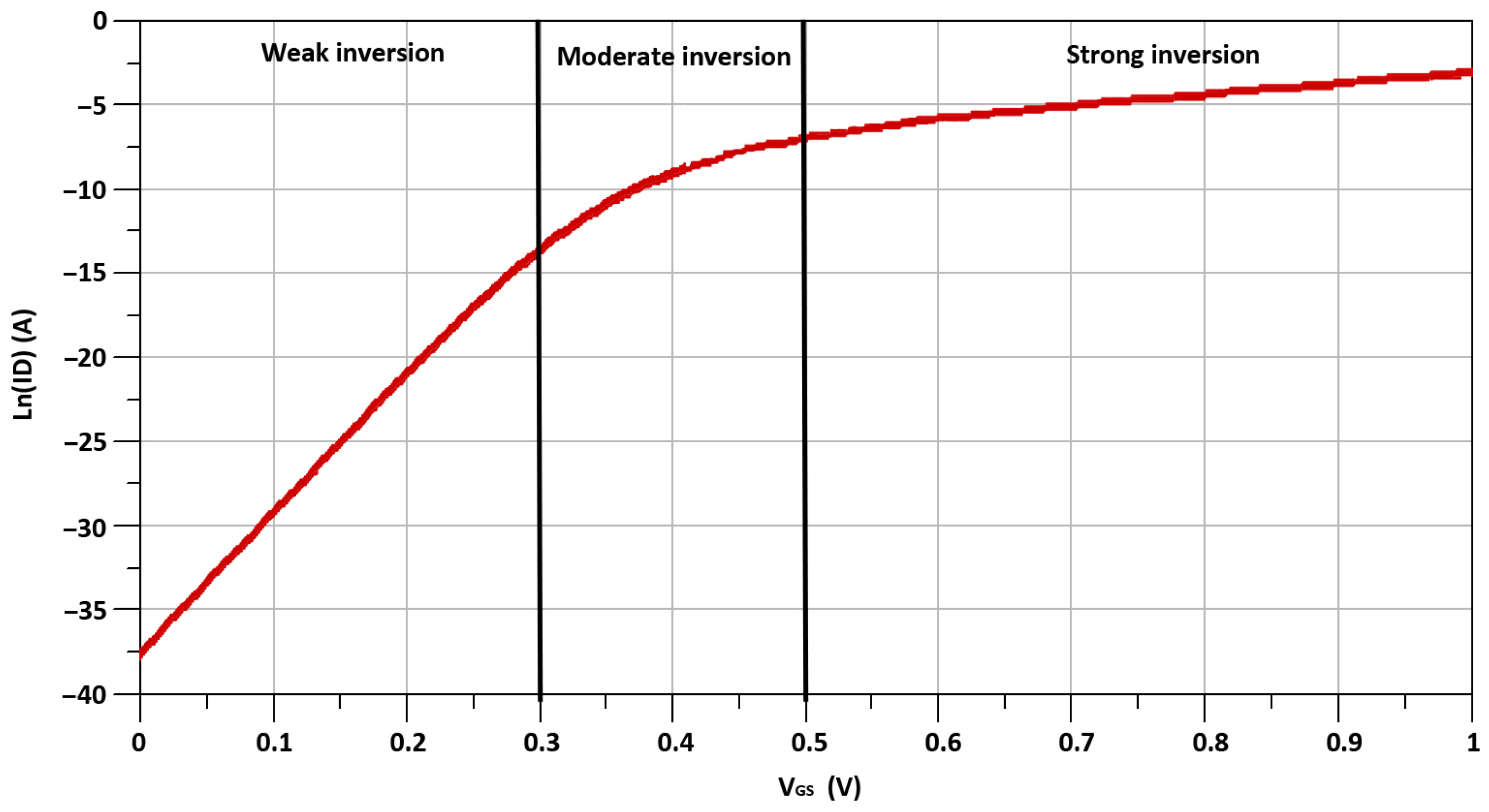
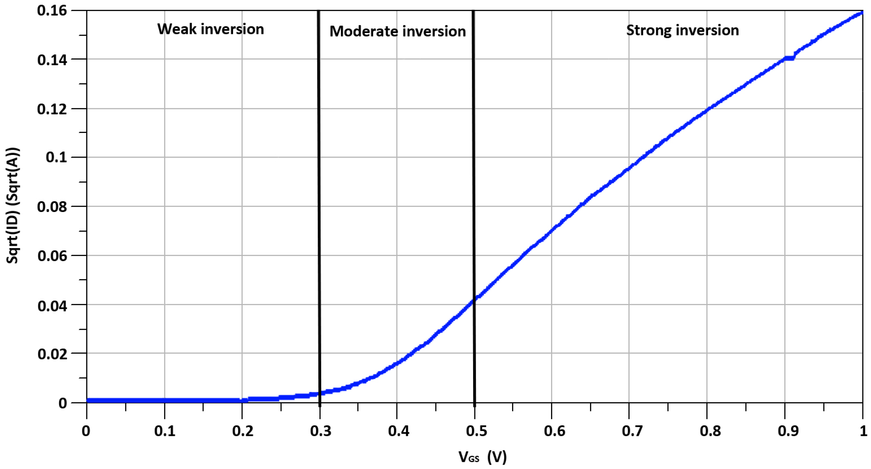
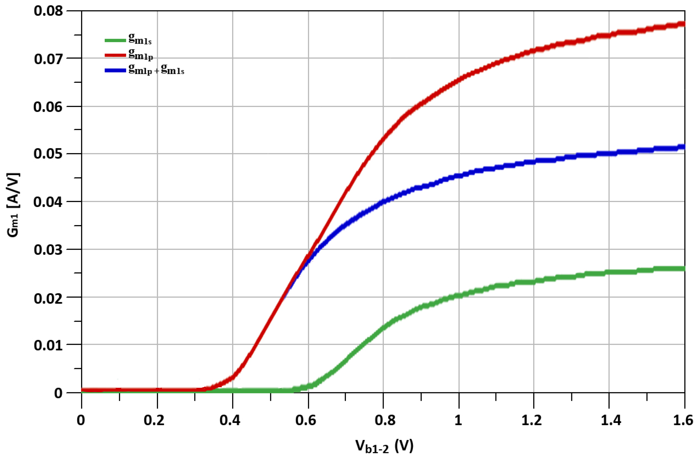
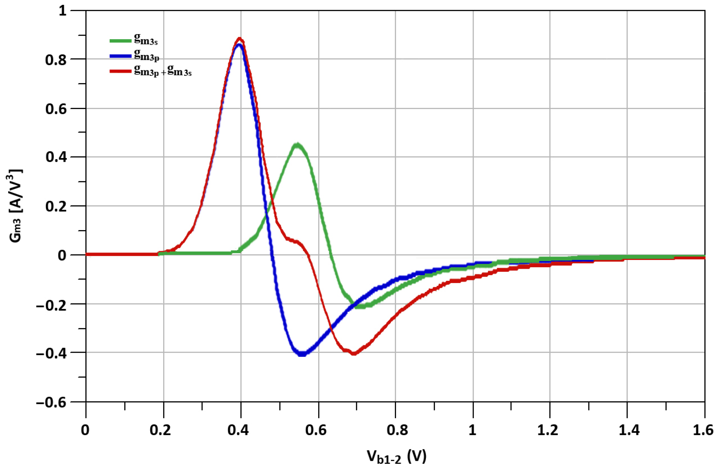
2.1. Linearity Analysis
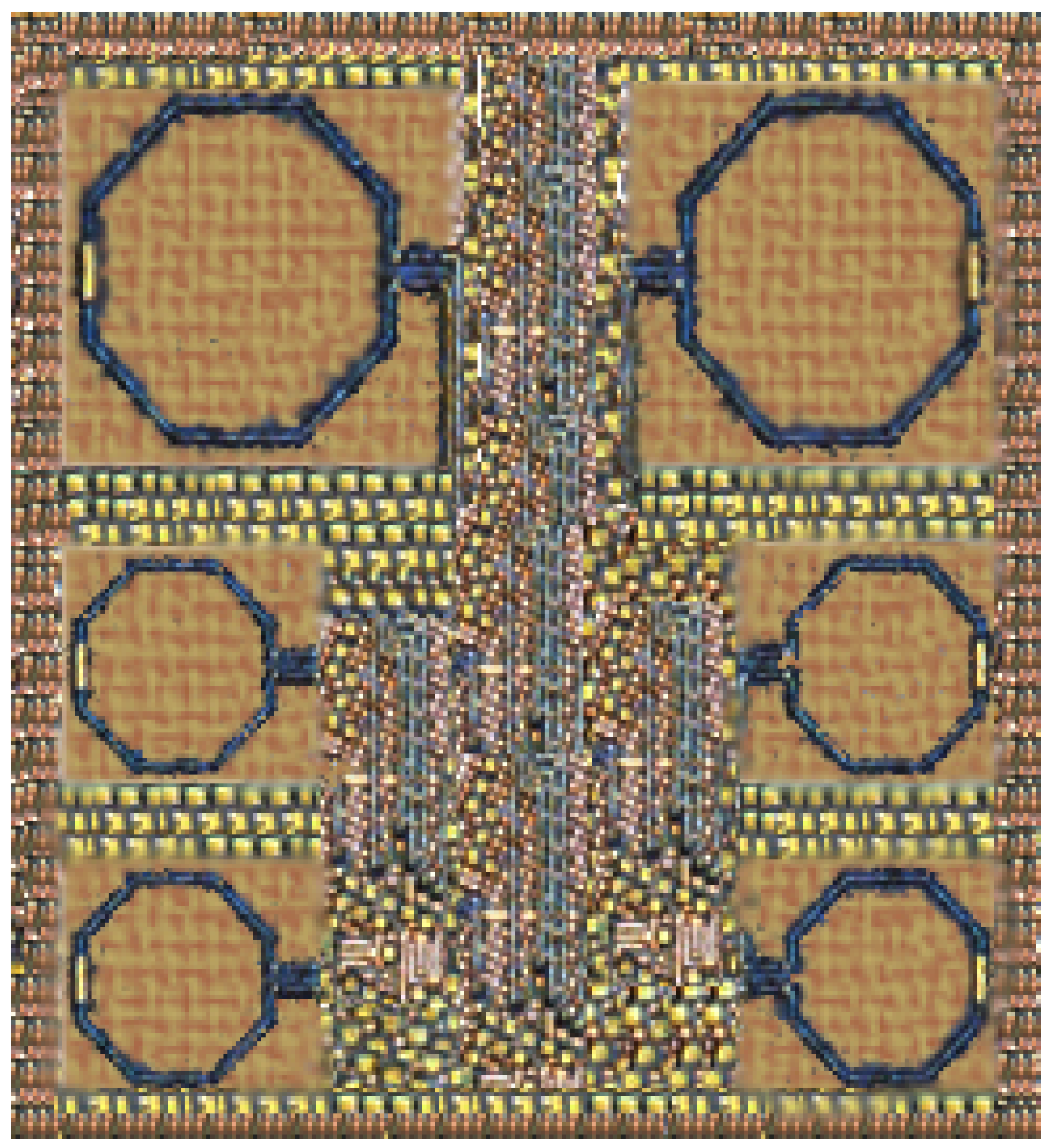
2.2. Layout Issues
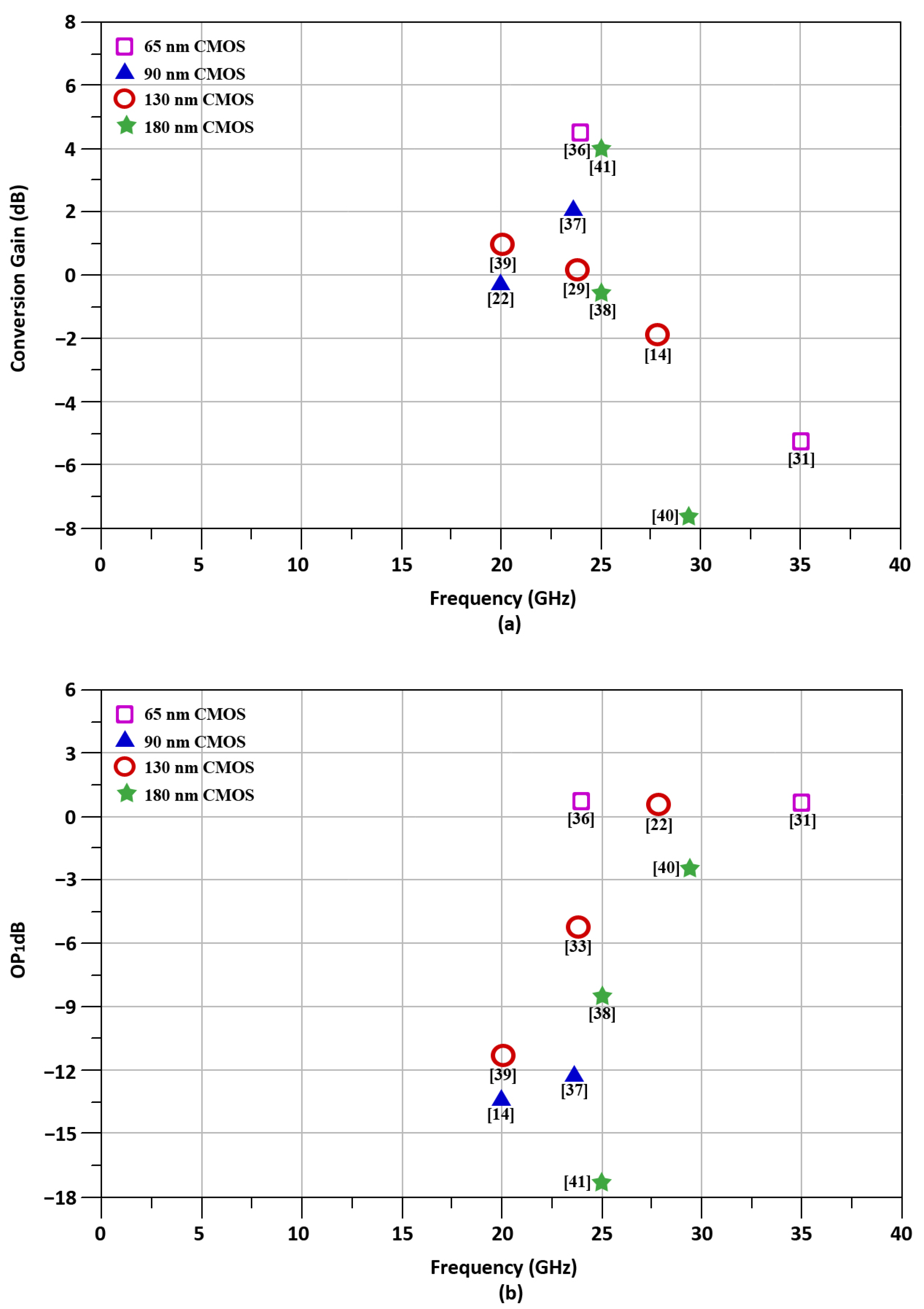
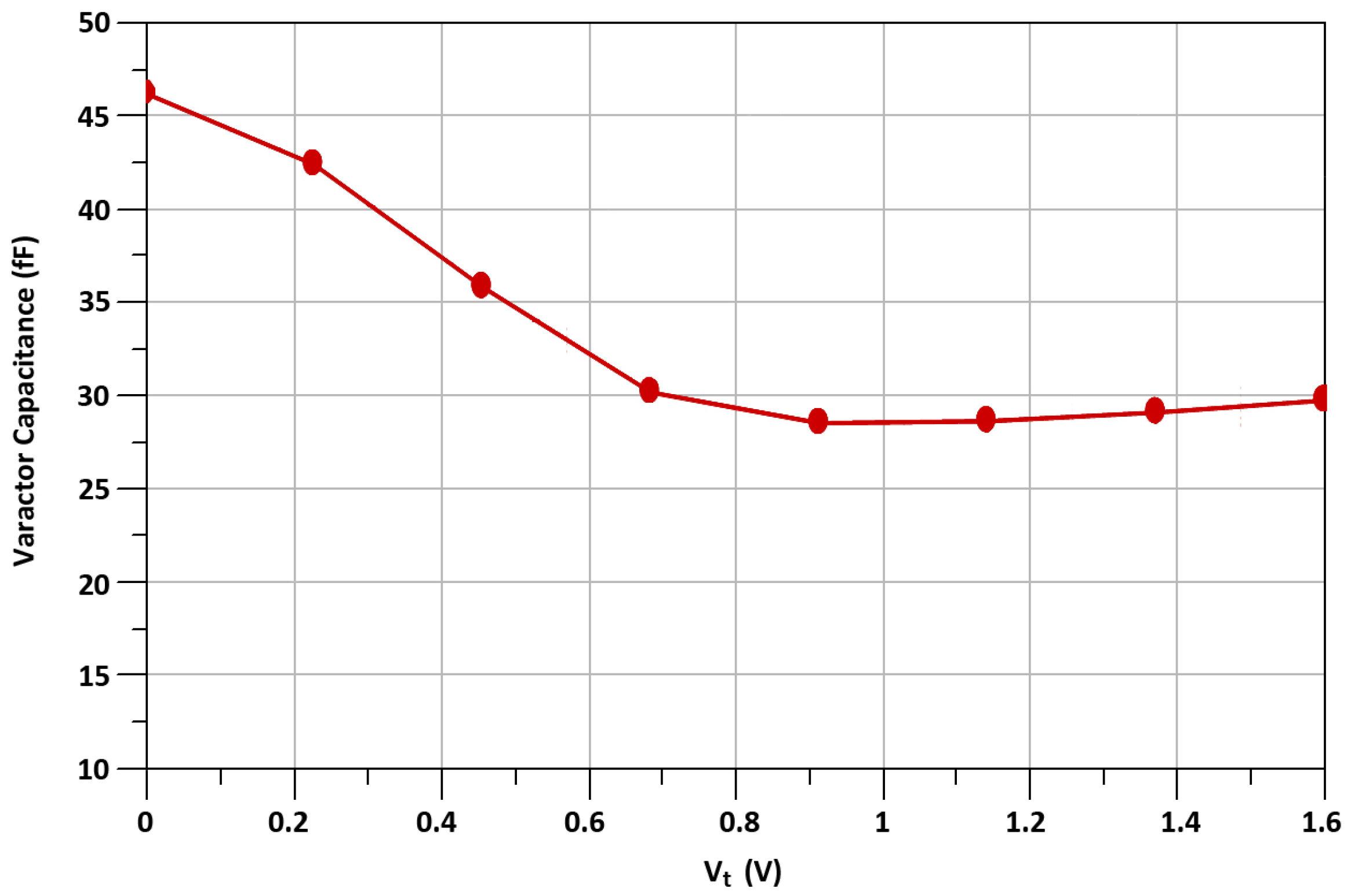
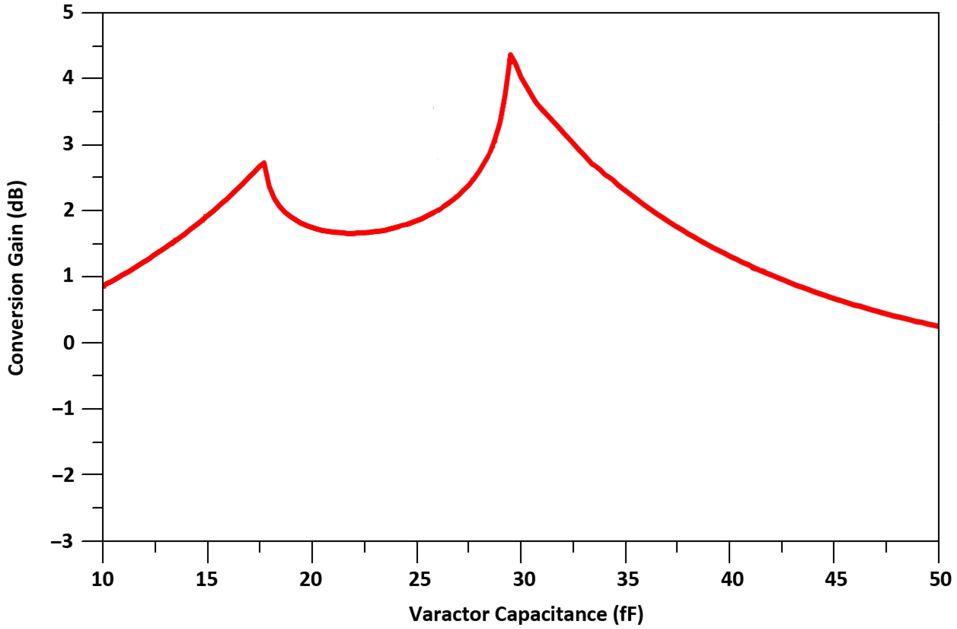
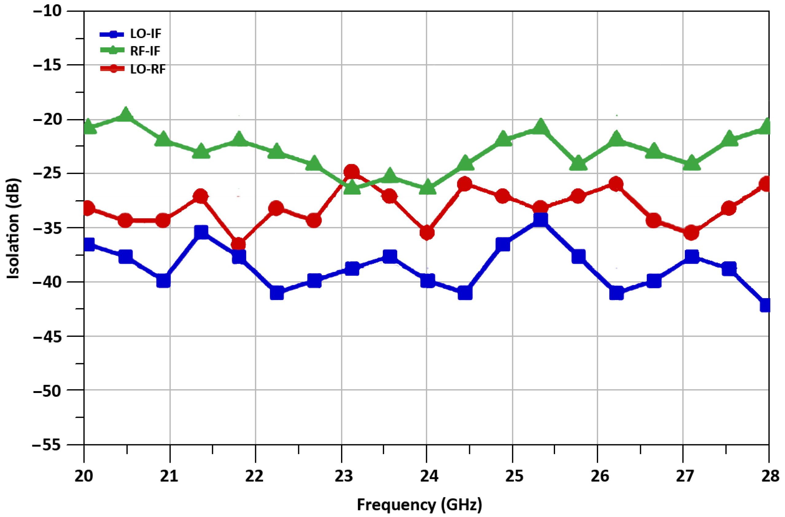
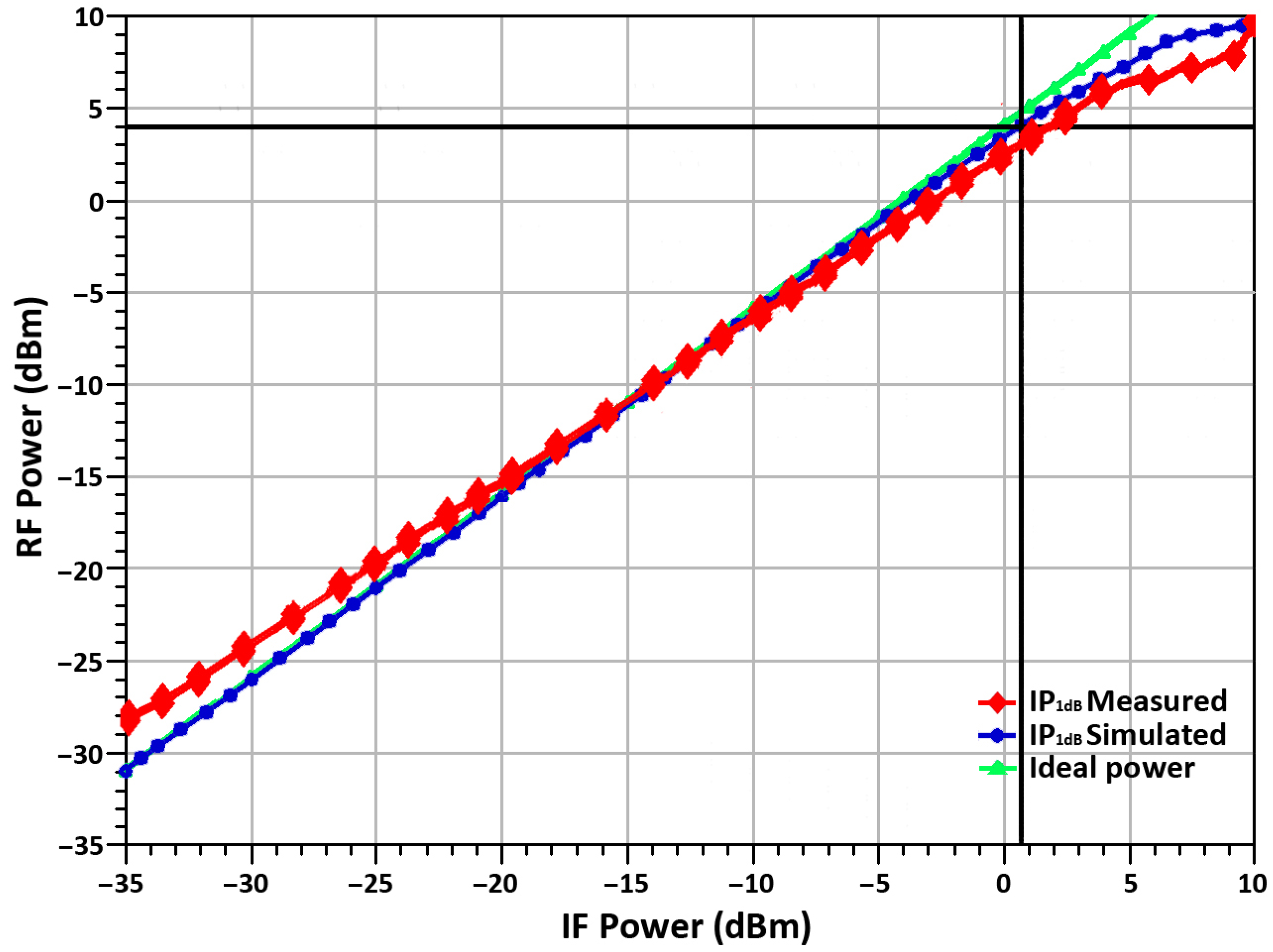
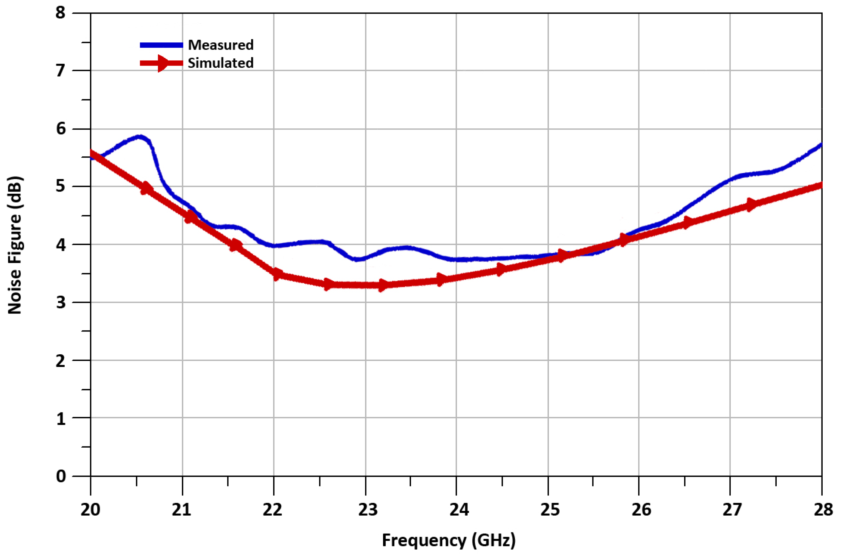
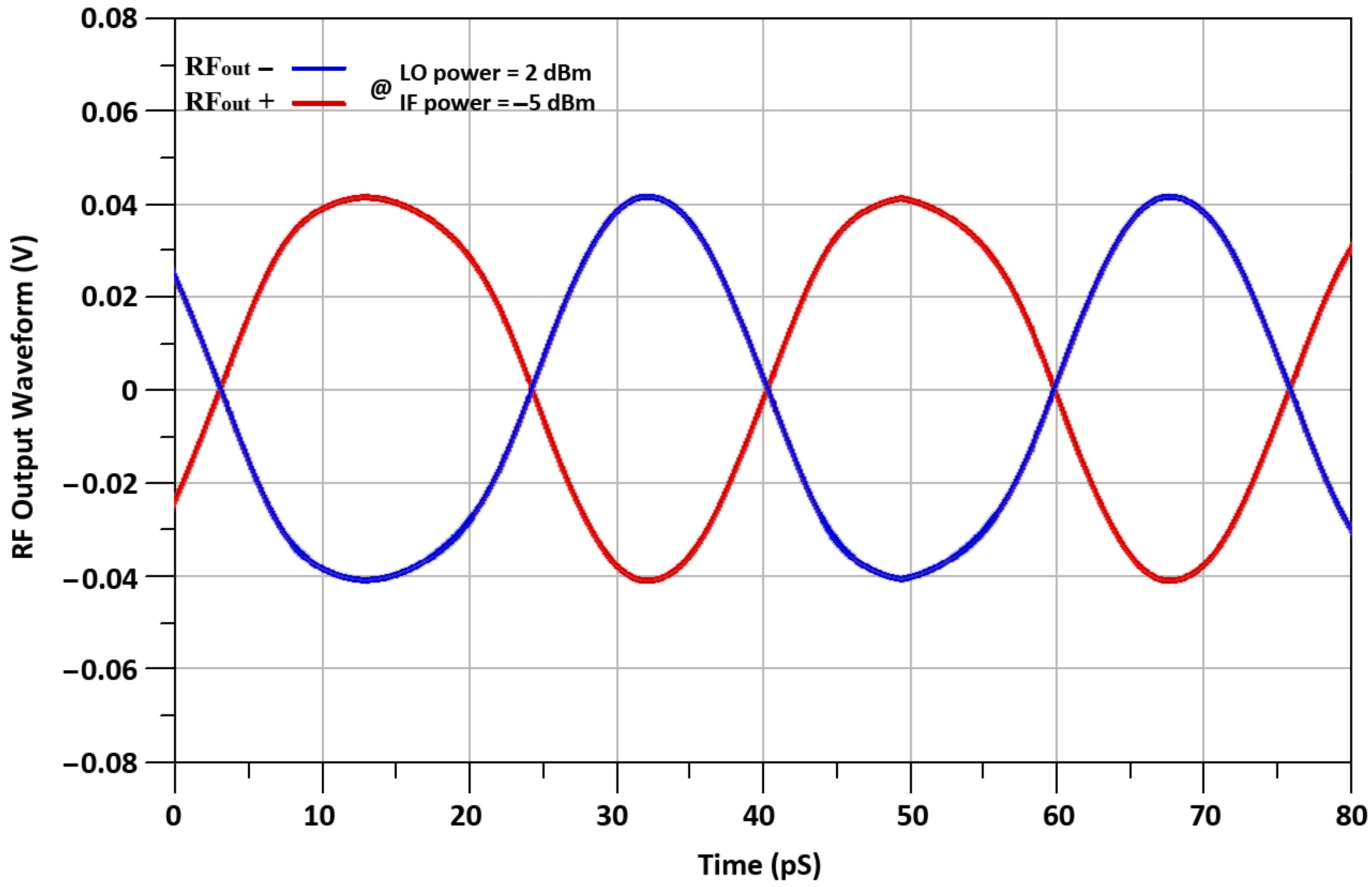
3. Results and Discussion
Proposed Mixer vs. State-of-the-Art Designs
4. Conclusions
Author Contributions
Funding
Institutional Review Board Statement
Informed Consent Statement
Data Availability Statement
Acknowledgments
Conflicts of Interest
References
- Qayyum, J.A.; Albrecht, J.D.; Ulusoy, A.C. A compact V-band upconversion mixer with −1.4 dBm OP1dB in SiGe HBT technology. IEEE Microw. Wirel. Components Lett. 2019, 29, 276–278. [Google Scholar] [CrossRef]
- Ayesha, A.; Rahman, M.; Haider, A.; Majeed Chaudhry, S. On Self-Interference Cancellation and Non-Idealities Suppression in Full-Duplex Radio Transceivers. Mathematics 2021, 9, 1434. [Google Scholar] [CrossRef]
- Siddique, A.; Delwar, T.S.; Kurbanov, M.; Ryu, J.Y. Low-power low-phase noise VCO for 24 GHz applications. Microelectron. J. 2020, 97, 104720. [Google Scholar] [CrossRef]
- Chen, Q.B.; Schaeffer, J.K. 22FDX Embracing IoT, 5G, and Automotive Applications-A Perspective through Global Research. In Proceedings of the 2019 IEEE SOI-3D-Subthreshold Microelectronics Technology Unified Conference (S3S), San Jose, CA, USA, 14–17 October 2019; pp. 1–5. [Google Scholar]
- Siddique, A.; Ryu, J.Y. A 24 GHz frequency synthesizer for automotive collision avoidance radar. Int. J. Electron. Lett. 2020, 8, 1–16. [Google Scholar] [CrossRef]
- Li, D.; Xia, Q.; Huang, J.; Li, J.; Chang, H.; Sun, B.; Liu, H. A 24 GHz Direct Conversion Receiver for FMCW Ranging Radar Based on Low Flicker Noise Mixer. Electronics 2021, 10, 722. [Google Scholar] [CrossRef]
- Voltti, M.; Koivisto, T.; Tiiliharju, E. Comparison of active and passive mixers. In Proceedings of the 2007 18th European Conference on Circuit Theory and Design, Seville, Spain, 27–30 August 2007; pp. 890–893. [Google Scholar]
- El-Desouki, M.M.; Qasim, S.M.; BenSaleh, M.S.; Deen, M.J. Toward realization of 2.4 GHz balunless narrowband receiver front-end for short range wireless applications. Sensors 2015, 15, 10791–10805. [Google Scholar] [CrossRef] [PubMed] [Green Version]
- Zumbahlen, H. Linear Circuit Design Handbook; Newnes/Elsevier: Wilmington, MA, USA, 2008. [Google Scholar]
- Siddiqi, A.A. Design Methodology and Investigation of GHz Range CMOS RF Mixers. Master’s Thesis, Carleton University, Ottawa, ON, Canada, 2000. [Google Scholar]
- Asad, B.Z.J. Low-Noise 24 GHz 0.15 μm GaAs pHEMT Gilbert Cell Mixer for Intelligent Transportation System Radar Receiver. Master’s Thesis, Ottawa-Carleton Institute for Electrical and Computer Engineering, Ottawa, ON, Canada, 2014. [Google Scholar]
- Arun, J.; Ezra, K.; Nithin, M.; Ravi, S. Design and Analysis of Double Balanced Gilbert Cell CMOS Mixer for Heterodyne receivers. Int. J. Appl. Eng. Res. 2013, 8, 2413–2416. [Google Scholar]
- Hu, X. RF CMOS Tunable Gilbert Mixer with Wide Tuning Frequency and Controllable Bandwidth: Design Sythesis and Verification. Master’s Thesis, Department of Electrical Engineering, Wright State University, Dayton, OH, USA, 2017. [Google Scholar]
- Ellinger, F.; Rodoni, L.C.; Sialm, G.; Kromer, C.; von Buren, G.; Schmatz, M.L.; Menolfi, C.; Toifl, T.; Morf, T.; Kossel, M.; et al. 30–40-GHz drain-pumped passive-mixer MMIC fabricated on VLSI SOI CMOS technology. IEEE Trans. Microw. Theory Technol. 2004, 52, 1382–1391. [Google Scholar] [CrossRef]
- Yang, H.-Y.; Tsai, J.-H.; Huang, T.-W.; Wang, H. Analysis of a new 33–58-GHz doubly balanced drain mixer in 90-nm CMOS technology. IEEE Trans. Microw. Theory Technol. 2012, 60, 1057–1068. [Google Scholar] [CrossRef]
- Sedighi, S.; Hashemipour, O.; Dousti, M. A 2.4-GHz highly linear derivative superposition Gilbert cell mixer. Turk. J. Electr. Eng. Comput. Sci. 2016, 24, 571–579. [Google Scholar] [CrossRef]
- Murad, S.A.Z.; Shahimin, M.M.; Pokharel, R.K.; Kanaya, H.; Yoshida, K. Linearity improvement of 5.2-GHz CMOS up-conversion mixer for wireless applications. Microw. Opt. Technol. Lett. 2012, 54, 923–925. [Google Scholar] [CrossRef]
- Zhang, F.; Skafidas, E.; Shieh, W.; Yang, B.; Wicks, B.N.; Liu, Z. A 60-GHz double-balanced mixer for direct up-conversion transmitter on 130-nm CMOS. In Proceedings of the 2008 IEEE Compound Semiconductor Integrated Circuits Symposium, Monterey, CA, USA, 12–15 October 2008; pp. 1–4. [Google Scholar]
- Won, Y.S.; Kim, C.H.; Lee, S.G. A 24 GHz Highly Linear Up-Conversion Mixer in CMOS 0.13 μm Technology. IEEE Microw. Wirel. Components Lett. 2015, 25, 400–402. [Google Scholar] [CrossRef]
- Wan, Q.; Wang, C.; Sun, J. Design of a low voltage highly linear 2.4 GHz up-conversion mixer in 0.18 μm CMOS technology. Wirel. Pers. Commun. 2013, 70, 57–68. [Google Scholar] [CrossRef]
- Siddique, A.; Delwar, T.S.; Ryu, J.Y. A high-linearity high-gain up-conversion mixer for 24 GHz automotive radar applications. Electron. Lett. 2021, 57, 48–50. [Google Scholar] [CrossRef]
- Xavier, B.A.; Sullivan, P.J.; Fransis, B.; Ku, W. A 0.9 V 960 MHz CMOS radio front end employing a doubly balanced transconductance mixer. In Proceedings of the Solid-State Circuits Conference, Southampton, UK, 16–18 September 1997; pp. 404–407. [Google Scholar]
- Lin, Y.S.; Wen, W.C.; Wang, C.C. 13.6 mW 79 GHz CMOS up-conversion mixer with 2.1 dB gain and 35.9 dB LO-RF isolation. IEEE Microw. Wirel. Components Lett. 2013, 24, 126–128. [Google Scholar] [CrossRef]
- Chen, A.Y.K.; Baeyens, Y.; Chen, Y.K.; Lin, J. An 80 GHz High Gain Double-Balanced Active Up-Conversion Mixer Using 0.18 μm SiGe BiCMOS Technology. IEEE Microw. Wirel. Components Lett. 2011, 21, 326–328. [Google Scholar] [CrossRef]
- Lee, C.P.; Behzad, A.; Ojo, D.; Kappes, M.; Au, S.; Pan, M.A.; Carter, K.; Tian, S. A highly linear direct-conversion transmit mixer transconductance stage with local oscillation feedthrough and I/Q imbalance cancellation scheme. In Proceedings of the 2006 IEEE International Solid State Circuits Conference—Digest of Technical Papers, San Francisco, CA, USA, 6–9 February 2006; pp. 1450–1459. [Google Scholar]
- Syu, J.-S.; Meng, C. 2.4/5.7 GHz dual-band high linearity Gilbert upconverter utilizing bias-offset TCA and LC current combiner. IEEE Microw. Compon. Lett. 2007, 17, 876–878. [Google Scholar] [CrossRef]
- Chiou, H.-K.; Chou, H.-T. A 0.4 V microwatt power consumption current-reused up-conversion mixer. IEEE Microw. Compon. Lett. 2013, 23, 40–42. [Google Scholar] [CrossRef]
- Codega, N.; Rossi, P.; Pirola, A.; Liscidini, A.; Castello, R. A currentmode, low out-of-band noise LTE transmitter with a class-A/B power mixer. IEEE J. Solid-State Circuits 2014, 49, 1627–1638. [Google Scholar] [CrossRef]
- Li, J.; Gu, Q.J. Harmonic-based nonlinearity factorization of switching behavior in up-conversion mixers. IEEE Trans. Circuits Syst. Reg. Pap. 2019, 66, 2468–2477. [Google Scholar] [CrossRef]
- Wang, X.; Dengi, A.; Kiaei, S. A high IIP3 -band BiCMOS mixer for radar applications. Proc. Int. Circuits Syst. Symp. 2004, 1, I-113–I-116. [Google Scholar]
- Gilbert, B. The micromixer: A highly linear variant of the Gilbert mixer using a bisymmetric class-AB input stage. IEEE Solid-State Circuits 1997, 32, 1412–1423. [Google Scholar] [CrossRef]
- Tseng, S.C.; Meng, C.C.; Chang, C.-H.; Wu, C.-K.; Huang, G.-W. Monolithic broadband Gilbert micromixer with an integrated Marchand balun using standard silicon ic process. IEEE Trans. Microw. Theory Technol. 2006, 54, 4362–4371. [Google Scholar] [CrossRef] [Green Version]
- Sivonen, P.; Vilander, A.; Parssinen, A. Cancellation of second orderintermodulation distortion and enhancement of IIP2 in common source and common-emitter RF transconductors. IEEE Trans. Circuits Syst. Reg. Pap. 2005, 52, 305–317. [Google Scholar] [CrossRef]
- Bao, M.; Li, Y.; Cathelin, A. A 23 GHz active mixer with integrated diode linearizer in SiGe BiCMOS technology. In Proceedings of the 33rd European Microwave Conference Proceedings (IEEE Cat. No.03EX723C), Munich, Germany, 7 October 2003; pp. 391–393. [Google Scholar]
- Tseng, S.-C.; Meng, C.C.; Wu, C.-K. GaInP/GaAs HBT wideband transformer Gilbert downconverter with low voltage supply. Electron. Lett. 2008, 44, 127–128. [Google Scholar] [CrossRef] [Green Version]
- Chen, J.H.; Kuo, C.C.; Hsin, Y.M.; Wang, H. A 15–50 GHz broadband resistive FET ring mixer using 0.18 μm CMOS technology. In Proceedings of the 2010 IEEE MTT-S International Microwave Symposium, Anaheim, CA, USA, 23–28 May 2010; pp. 784–787. [Google Scholar]
- Lai, I.C.; Fujishima, M. An integrated 20–26 GHz CMOS up-conversion mixer with low power consumption. In Proceedings of the 32nd European Solid-State Circuits Conference, Montreaux, Switzerland, 19–21 September 2006; pp. 400–403. [Google Scholar]
- Comeau, J.P.; Cressler, J.D. A 28-GHz SiGe up-conversion mixer using a series-connected triplet for higher dynamic range and improved IF port return loss. IEEE J. Solid-State Circuits 2006, 41, 560–565. [Google Scholar] [CrossRef]
- Lin, Y.H.; Li, Y.C.; Lin, W.J.; Tsai, J.H.; Alshehri, A.; Almalki, M.; Sayed, A.; Huang, T.W. A Ka-band High Linearity Up-Conversion Mixer with LO Boosting Linearization Technique. In Proceedings of the 2018 48th European Microwave Conference (EuMC), Madrid, Spain, 23–27 September 2018; pp. 259–262. [Google Scholar]
- Madihian, M.; Desclos, L.; Maruhashi, K.; Onda, K.; Kuzuhara, M. A monolithic AlGaAs/InGaAs upconverter IC for K-Band wireless networks. IEEE Trans. Microw. Theory Tech. 1995, 43, 2773–2777. [Google Scholar] [CrossRef]
- Tsai, J.-H.; Lin, W.-H.; Huang, C.-J. Design of 15–34 GHz low-power up-conversion ring mixer using 0.18 μm CMOS technology. In Proceedings of the 2016 IEEE International Symposium on Radio-Frequency Integration Technology (RFIT), Taipei, Taiwan, 24–26 August 2016; pp. 1–3. [Google Scholar]
- Aparin, V.; Larson, L.E. Modified derivative superposition method for linearizing FET low-noise amplifiers. IEEE Trans. Microw. Theory Tech. 2005, 53, 571–581. [Google Scholar] [CrossRef]
- Chen, Z.; Liu, Z.; Jiang, Z.; Liu, P.; Liu, H.; Wu, Y.; Zhao, C.; Kang, K. A 27.5–43.5 GHz high linearity up-conversion CMOS mixer for 5G communication. In Proceedings of the 2017 IEEE Electrical Design of Advanced Packaging and Systems Symposium (EDAPS), Haining, China, 14–16 December 2017; pp. 1–3. [Google Scholar]
- Valdes-Garcia, A.; Reynolds, S.; Plouchart, J.-O. 60 GHz transmitter circuits in 65 nm CMOS. In Proceedings of the 2008 IEEE Radio Frequency Integrated Circuits Symposium, Atlanta, GA, USA, 15–17 June 2008; pp. 641–644. [Google Scholar]
- Verma, A.; O, K.K.; Lin, J. A low-power up conversion CMOS mixer for 22–29-GHz ultra-wideband applications. IEEE Trans. Microw. Theory Tech. 2006, 54, 3295–3300. [Google Scholar] [CrossRef]
- Zhu, F.; Wang, K.; Wu, K. A reconfigurable low-voltage and low-power millimeter-wave dual-band mixer in 65-nm CMOS. IEEE Access 2019, 7, 33359–33368. [Google Scholar] [CrossRef]
- Motieifar, A.; Pour, Z.A.; Bridges, G.; Shafai, C.; Shafai, L. An ultra wideband mixer with integrated impedance-matching circuit. In Proceedings of the 2006 12th International Symposium on Antenna Technology and Applied Electromagnetics and Canadian Radio Sciences Conference, Montreal, QC, Canada, 17–19 July 2006; pp. 1–4. [Google Scholar]
- Wan, Q.; Wang, C.; Yu, F. Design of a 2.4 GHz High-Performance Up-Conversion Mixer with Current Mirror Topology. Radioengineering 2012, 21, 752–757. [Google Scholar]
- Sapone, G.; Palmisano, G. A 1.5-V 0.25-μm CMOS up-converter for 3–5 GHz low-power WPANs. Microw. Opt. Technol. Lett. 2007, 49, 2209–2212. [Google Scholar] [CrossRef]


| Element | Dimension |
|---|---|
| M1, M2 | 31 m/65 nm |
| Mp | 53 m/65 nm |
| Ms | 41 m/65 nm |
| M3–M6 | 37 m/65 nm |
| Mcv | 34 m/65 nm |
| L1–L2 | 175 pH |
| Ls1 | 70 pH |
| Ls2 | 90 pH |
| C3–C6 | 45 fF |
| Cv1–Cv2 | 29.3 fF @ Vt = 0.75 V |
| Ref. | Process (nm) | RF Freq. (GHz) | Gain (dB) | OP1dB | Chip Area (mm) | Power Consumption (mW) | NF |
|---|---|---|---|---|---|---|---|
| [19], 2015 | 130 | 23.4–29.2 | −1.9 | 0.3 | 0.8 | 38 | NA |
| [21], 2021 | 65 | 24 | 4.7 | 0.41 | 0.42 | 5.2 | 3.8 |
| [43], 2017 | 65 | 27.5–43.5 | −5 | 0.42 | 0.686 | 14 | NA |
| [44], 2008 | 65 | 60 | −6.5 | −5 | 0.98 | 29 | NA |
| [45], 2006 | 130 | 18–28 | 0.7 | −5.2 | 0.46 | 22.8 | NA |
| [46], 2019 | 65 | 17–43 | 1.6 | NA | 0.5 | NA | 12.4 |
| [47], 2006 | 180 | 3.1–10.6 | 10 | NA | 1 | NA | 10 |
| [48], 2012 | 180 | 2.4 | 7.1 | NA | 0.4 | 4.5 | 11.9 |
| [49], 2007 | 250 | 3.5 | 3.8 | NA | 0.34 | 3.5 | 8 |
| [This Work] | 65 | 24 | 4.1 | 4.1 | 0.4 | 4.9 | 3.8 |
Publisher’s Note: MDPI stays neutral with regard to jurisdictional claims in published maps and institutional affiliations. |
© 2021 by the authors. Licensee MDPI, Basel, Switzerland. This article is an open access article distributed under the terms and conditions of the Creative Commons Attribution (CC BY) license (https://creativecommons.org/licenses/by/4.0/).
Share and Cite
Siddique, A.; Delwar, T.S.; Behera, P.; Biswal, M.R.; Haider, A.; Ryu, J.-Y. Design and Analysis of a Novel 24 GHz Up-Conversion Mixer with Improved Derivative Super-Position Linearizer Technique for 5G Applications. Sensors 2021, 21, 6118. https://doi.org/10.3390/s21186118
Siddique A, Delwar TS, Behera P, Biswal MR, Haider A, Ryu J-Y. Design and Analysis of a Novel 24 GHz Up-Conversion Mixer with Improved Derivative Super-Position Linearizer Technique for 5G Applications. Sensors. 2021; 21(18):6118. https://doi.org/10.3390/s21186118
Chicago/Turabian StyleSiddique, Abrar, Tahesin Samira Delwar, Prangyadarsini Behera, Manas Ranjan Biswal, Amir Haider, and Jee-Youl Ryu. 2021. "Design and Analysis of a Novel 24 GHz Up-Conversion Mixer with Improved Derivative Super-Position Linearizer Technique for 5G Applications" Sensors 21, no. 18: 6118. https://doi.org/10.3390/s21186118