Fabrication of ZnO Thin Films Doped with Na at Different Percentages for Sensing CO2 in Small Quantities at Room Temperature


Abstract
:1. Introduction
2. Materials and Methods
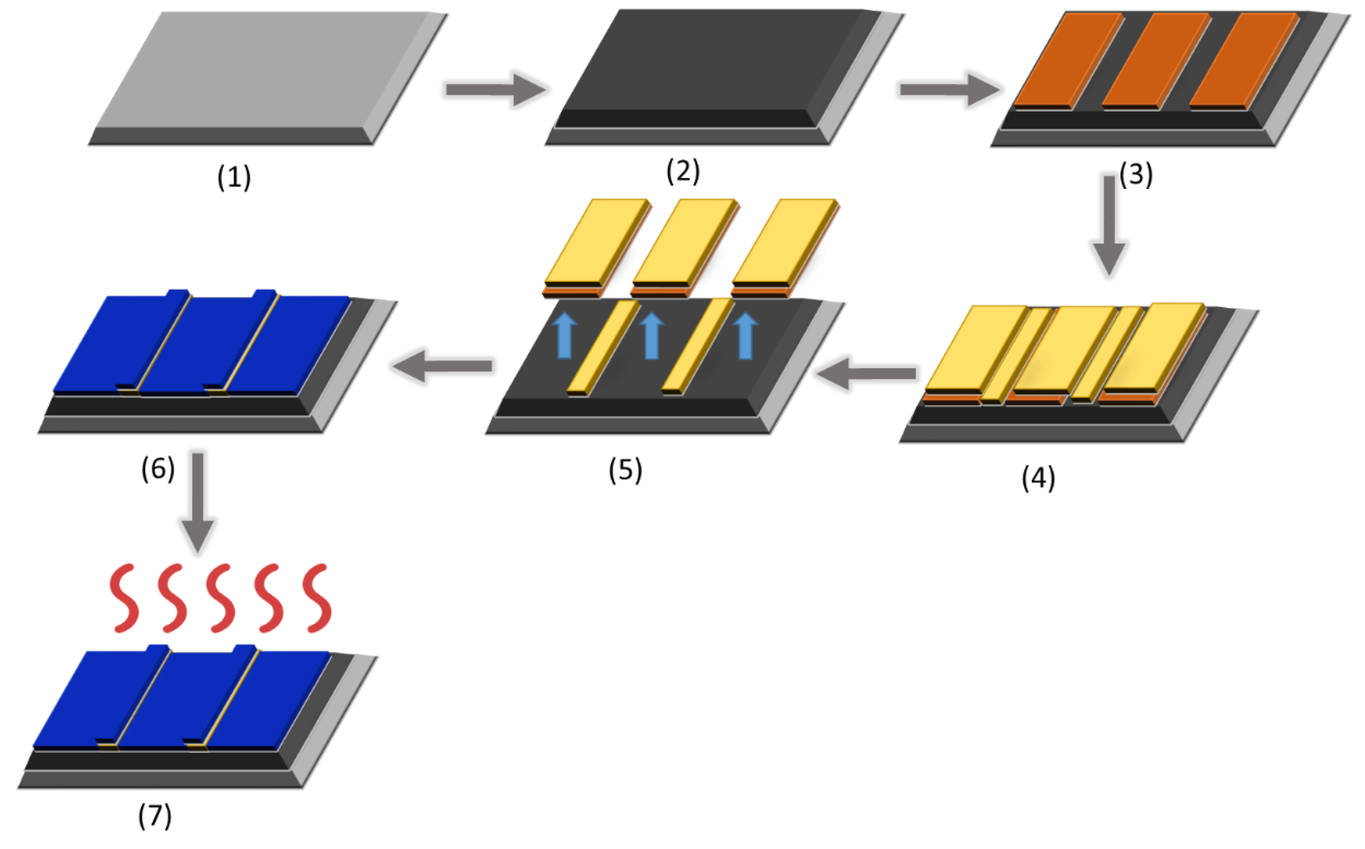
2.1. Sol-Gel Preparation, Film Deposition, and Substrate Development
2.2. Sensor Fabrication
2.3. Morphological and Crystallograpic Characterisation
2.4. Electrical Characterization
3. Results
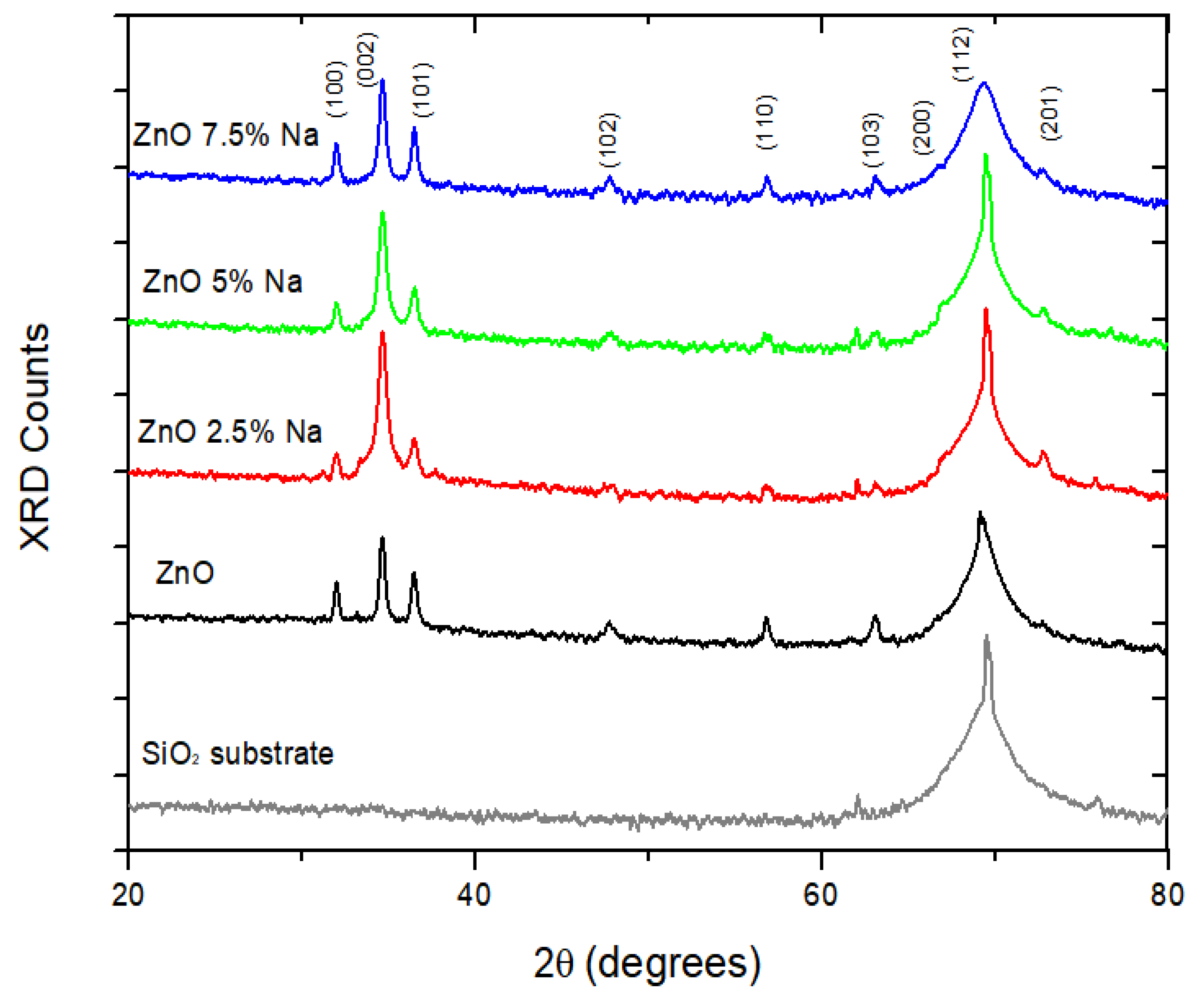
3.1. X-Ray Diffraction (XRD)
3.2. Field Emission-Scanning Electron Microscopy (FE-SEM)
3.3. Atomic Force Microscopy (AFM)
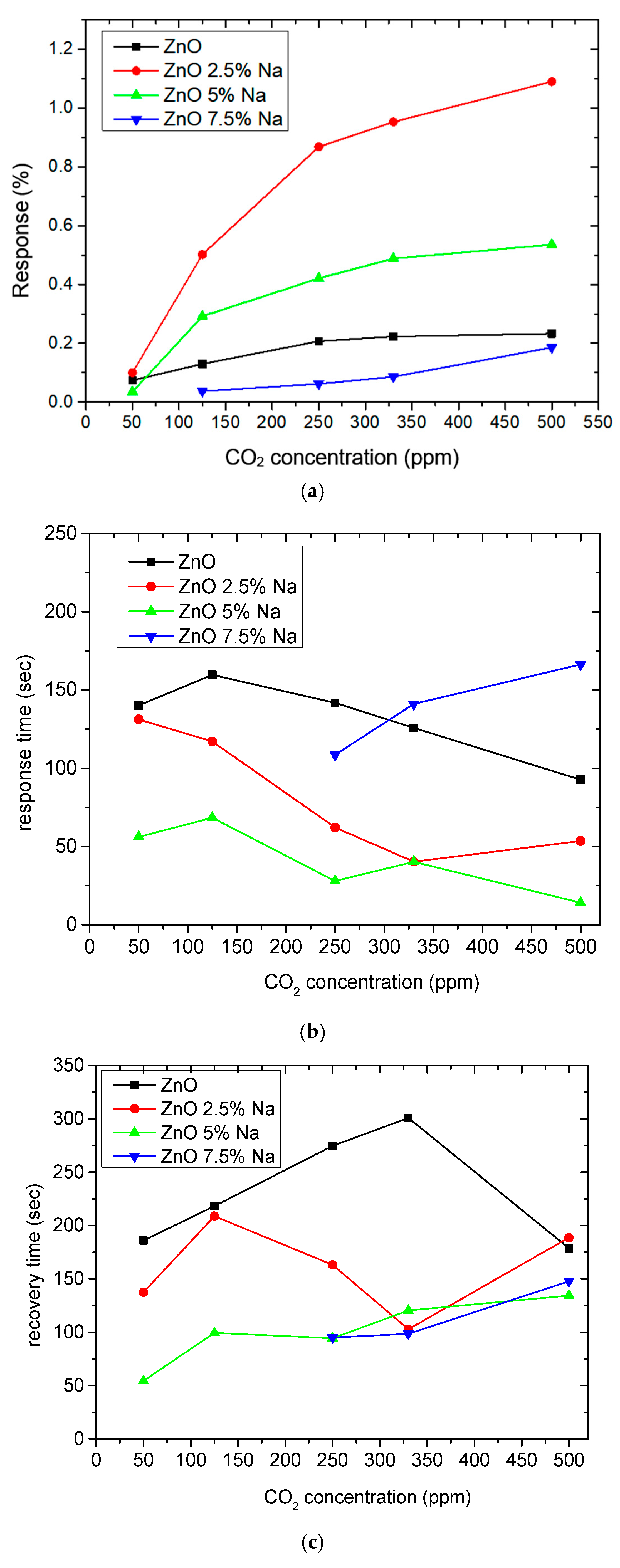
3.4. CO2 Measurements
4. Conclusions
Author Contributions
Funding
Institutional Review Board Statement
Informed Consent Statement
Data Availability Statement
Acknowledgments
Conflicts of Interest
References
- de Cássia Martins Salomão, B. Pathogens and Spoilage Microorganisms in Fruit Juice: An Overview. In Fruit Juices; Elsevier Inc.: Amsterdam, The Netherlands, 2018; pp. 291–308. [Google Scholar] [CrossRef]
- Mustafa, F.; Andreescu, S. Chemical and Biological Sensors for Food-Quality Monitoring and Smart Packaging. Foods 2018, 7, 168. [Google Scholar] [CrossRef] [PubMed]
- Mafe, A.N.; Edo, G.I.; Makia, R.S.; Joshua, O.A.; Akpoghelie, P.O.; Gaaz, T.S.; Jikah, A.N.; Yousif, E.; Isoje, E.F.; Igbuku, U.A.; et al. A review on food spoilage mechanisms, food borne diseases and commercial aspects of food preservation and processing. Food Chem. Adv. 2024, 5, 100852. [Google Scholar] [CrossRef]
- Joshi, N.; Pransu, G.; Adam Conte-Junior, C. Critical Review and Recent Advances of 2D Materials-Based Gas Sensors for Food Spoilage Detection. Crit. Rev. Food Sci. Nutr. 2022, 63, 10536–10559. [Google Scholar] [CrossRef]
- Gobbi, E.; Falasconi, M.; Concina, I.; Mantero, G.; Bianchi, F.; Mattarozzi, M.; Musci, M.; Sberveglieri, G. Electronic Nose and Alicyclobacillus Spp. Spoilage of Fruit Juices: An Emerging Diagnostic Tool. Food Control 2010, 21, 1374–1382. [Google Scholar] [CrossRef]
- Weston, M.; Geng, S.; Chandrawati, R. Food Sensors: Challenges and Opportunities. Adv. Mater. Technol. 2021, 6, 2001242. [Google Scholar] [CrossRef]
- Pavase, T.R.; Lin, H.; Shaikh, Q.; Hussain, S.; Li, Z.; Ahmed, I.; Lv, L.; Sun, L.; Shah, S.B.H.; Kalhoro, M.T. Recent Advances of Conjugated Polymer (CP) Nanocomposite-Based Chemical Sensors and Their Applications in Food Spoilage Detection: A Comprehensive Review. Sens. Actuators B Chem. 2018, 273, 1113–1138. [Google Scholar] [CrossRef]
- Rezk, M.Y.; Sharma, J.; Gartia, M.R. Nanomaterial-Based CO2 Sensors. Nanomaterials 2020, 10, 2251. [Google Scholar] [CrossRef]
- Stramarkou, M.; Bardakas, A.; Krokida, M.; Tsamis, C. ZnO-Based Chemi-Resistive Sensors for CO2 Detection: A Review. Sens. Rev. 2022, 42, 682–706. [Google Scholar] [CrossRef]
- Kotbi, A.; Benyoussef, M.; Ressami, E.M.; Lejeune, M.; Lakssir, B.; Jouiad, M. Gas Sensors Based on Exfoliated G-C3N4 for CO2 Detection. Chemosensors 2022, 10, 470. [Google Scholar] [CrossRef]
- Dhahri, R.; Leonardi, S.G.; Hjiri, M.; El Mir, L.; Bonavita, A.; Donato, N.; Iannazzo, D.; Neri, G. Enhanced Performance of Novel Calcium/Aluminum Co-Doped Zinc Oxide for CO2 Sensors. Sens. Actuators B Chem. 2017, 239, 36–44. [Google Scholar] [CrossRef]
- Altun, B.; Karaduman Er, I.; Çağırtekin, A.O.; Ajjaq, A.; Sarf, F.; Acar, S. Effect of Cd Dopant on Structural, Optical and CO2 Gas Sensing Properties of ZnO Thin Film Sensors Fabricated by Chemical Bath Deposition Method. Appl. Phys. A Mater. Sci. Process 2021, 127, 687. [Google Scholar] [CrossRef]
- Franco, M.A.; Conti, P.P.; Andre, R.S.; Correa, D.S. A Review on Chemiresistive ZnO Gas Sensors. Sens. Actuators Rep. 2022, 4, 100100. [Google Scholar] [CrossRef]
- Bagheri, F.; Haratizadeh, H.; Ahmadi, M. Improving CO2 Sensing and P-n Conductivity Transition under UV Light by Chemo-Resistive Sensor Based on ZnO Nanoparticles. Ceram. Int. 2024, 50, 1497–1504. [Google Scholar] [CrossRef]
- Gong, J.; Li, Y.; Chai, X.; Hu, Z.; Deng, Y. UV-Light-Activated ZnO Fibers for Organic Gas Sensing at Room Temperature. J. Phys. Chem. C 2010, 114, 1293–1298. [Google Scholar] [CrossRef]
- Ghobadifard, M.; Khelghati, M.; Zamani, E.; Maleki, Q.; Farhadi, S.; Aslani, A. Zinc Oxide Nano-Crystals Assisted for Carbon Dioxide Gas Sensing; Prepared by Solvothermal and Sonochemical Methods. Iran. Chem. Commun. 2015, 3, 26–40. [Google Scholar]
- Duan, X.; Jiang, Y.; Liu, B.; Duan, Z.; Zhang, Y.; Yuan, Z.; Tai, H. Enhancing the Carbon Dioxide Sensing Performance of LaFeO3 by Co Doping. Sens. Actuators B Chem. 2024, 402, 135136. [Google Scholar] [CrossRef]
- González-Garnica, M.; Galdámez-Martínez, A.; Malagón, F.; Ramos, C.D.; Santana, G.; Abolhassani, R.; Kumar Panda, P.; Kaushik, A.; Mishra, Y.K.; Karthik, T.V.K.; et al. One Dimensional Au-ZnO Hybrid Nanostructures Based CO2 Detection: Growth Mechanism and Role of the Seed Layer on Sensing Performance. Sens. Actuators B Chem. 2021, 337, 129765. [Google Scholar] [CrossRef]
- Abdelkarem, K.; Saad, R.; El Sayed, A.M.; Fathy, M.I.; Shaban, M.; Hamdy, H. Design of High-Sensitivity La-Doped ZnO Sensors for CO2 Gas Detection at Room Temperature. Sci. Rep. 2023, 13, 18398. [Google Scholar] [CrossRef]
- Mishra, M.; Kumar, M. Effects of Al Doping on Structural, Optical, Morphological, and Low-Concentration CO2 Gas Sensing Properties of ZnO Nanoparticles Synthesized by Sol-Gel Method. Phys. Scr. 2024, 99, 125929. [Google Scholar] [CrossRef]
- Ghosh, A.; Zhang, C.; Zhang, H.; Shi, S. CO2 Sensing Behavior of Calcium-Doped ZnO Thin Film: A Study to Address the Cross-Sensitivity of CO2 in H2 and CO Environment. Langmuir 2019, 35, 10267–10275. [Google Scholar] [CrossRef]
- Soltabayev, B.; Raiymbekov, Y.; Nuftolla, A.; Turlybekuly, A.; Yergaliuly, G.; Mentbayeva, A. Sensitivity Enhancement of CO2 Sensors at Room Temperature Based on the CZO Nanorod Architecture. ACS Sens. 2024, 9, 1227–1238. [Google Scholar] [CrossRef] [PubMed]
- Basyooni, M.A.; Shaban, M.; El Sayed, A.M. Enhanced Gas Sensing Properties of Spin-Coated Na-Doped ZnO Nanostructured Films. Sci. Rep. 2017, 7, srep41716. [Google Scholar] [CrossRef] [PubMed]
- Zhu, L.; Zeng, W. Room-Temperature Gas Sensing of ZnO-Based Gas Sensor: A Review. Sens. Actuators A Phys. 2017, 267, 242–261. [Google Scholar] [CrossRef]
- Pantò, F.; Leonardi, S.G.; Fazio, E. CO2 Sensing Properties of Electro-Spun Ca-Doped ZnO Fi Bres. Nanotechnology 2018, 29, 305501. [Google Scholar] [CrossRef]
- Elsayed, M.H.; Elmorsi, T.M.; Abuelela, A.M.; Hassan, A.E.; Alhakemy, A.Z.; Bakr, M.F.; Chou, H.H. Direct Sunlight-Active Na-Doped ZnO Photocatalyst for the Mineralization of Organic Pollutants at Different PH Mediums. J. Taiwan Inst. Chem. Eng. 2020, 115, 187–197. [Google Scholar] [CrossRef]
- Akcan, D.; Gungor, A.; Arda, L. Structural and Optical Properties of Na-Doped ZnO Films. J. Mol. Struct. 2018, 1161, 299–305. [Google Scholar] [CrossRef]
- Dhawale, D.S.; Lokhande, C.D. Chemical Route to Synthesis of Mesoporous ZnO Thin Films and Their Liquefied Petroleum Gas Sensor Performance. J. Alloys Compd. 2011, 509, 10092–10097. [Google Scholar] [CrossRef]
- Pohle, R.; Tawil, A.; Mrotzek, C.; Fleischer, M. CO2 Sensing by Work Function Readout of ZnO Based Screen Printed Films. In Proceedings of the 2013 Transducers and Eurosensors XXVII: The 17th International Conference on Solid-State Sensors, Actuators and Microsystems, TRANSDUCERS and EUROSENSORS 2013, Barcelona, Spain, 16–20 June 2013. [Google Scholar] [CrossRef]
- Jaballah, S.; Dahman, H.; El Mir, L.; Neri, G.; Donato, N. CO and CO2 Sensing by Al-Mg-ZnO Based Conductometric Sensor. In Proceedings of the IEEE Medical Measurements and Applications, MeMeA 2020—Conference Proceedings, Bari, Italy, 1 June–1 July 2020. [Google Scholar] [CrossRef]
- Shokry Hassan, H.; Kashyout, A.B.; Morsi, I.; Nasser, A.A.A.; Ali, I. Synthesis, Characterization and Fabrication of Gas Sensor Devices Using ZnO and ZnO:In Nanomaterials. Beni Suef Univ. J. Basic. Appl. Sci. 2014, 3, 216–221. [Google Scholar] [CrossRef]
- Motaung, D.E.; Kortidis, I.; Mhlongo, G.H.; Duvenhage, M.M.; Swart, H.C.; Kiriakidis, G.; Ray, S.S. Correlating the Magnetism and Gas Sensing Properties of Mn-Doped ZnO Films Enhanced by UV Irradiation. RSC Adv. 2016, 6, 26227–26238. [Google Scholar] [CrossRef]
- Hunge, Y.M.; Yadav, A.A.; Kulkarni, S.B.; Mathe, V.L. A Multifunctional ZnO Thin Film Based Devises for Photoelectrocatalytic Degradation of Terephthalic Acid and CO2 Gas Sensing Applications. Sens. Actuators B Chem. 2018, 274, 1–9. [Google Scholar] [CrossRef]
- Samarasekara, P.; Yapa, N.U.S.; Kumara, N.T.R.N.; Perera, M.V.K. CO2 Gas Sensitivity of Sputtered Zinc Oxide Thin Films. Bull. Mater. Sci. 2007, 30, 113–116. [Google Scholar] [CrossRef]
- Lupan, O.; Chow, L.; Shishiyanu, S.; Monaico, E.; Shishiyanu, T.; Şontea, V.; Roldan Cuenya, B.; Naitabdi, A.; Park, S.; Schulte, A. Nanostructured Zinc Oxide Films Synthesized by Successive Chemical Solution Deposition for Gas Sensor Applications. Mater. Res. Bull. 2009, 44, 63–69. [Google Scholar] [CrossRef]
- Kannan, P.K.; Saraswathi, R.; Rayappan, J.B.B. CO2 Gas Sensing Properties of DC Reactive Magnetron Sputtered ZnO Thin Film. Ceram. Int. 2014, 40, 13115–13122. [Google Scholar] [CrossRef]
- Dhahri, R.; Hjiri, M.; El Mir, L.; Fazio, E.; Neri, F.; Barreca, F.; Donato, N.; Bonavita, A.; Leonardi, S.G.; Neri, G. ZnO:Ca Nanopowders with Enhanced CO2 Sensing Properties. J. Phys. D Appl. Phys. 2015, 48, 255503. [Google Scholar] [CrossRef]
- Shukla, R.K.; Srivastava, A.; Kumar, N.; Pandey, A.; Pandey, M. Optical and Sensing Properties of Cu Doped ZnO Nanocrystalline Thin Films. J. Nanotechnol. 2015, 2015, 172864. [Google Scholar] [CrossRef]
- Martínez, L.; Holguín-Momaca, J.T.; Karthik, T.V.K.; Olive-Méndez, S.F.; Campos-Alvarez, J.; Agarwal, V. Sputtering Temperature Dependent Growth Kinetics and CO2 Sensing Properties of ZnO Deposited over Porous Silicon. Superlattices Microstruct. 2016, 98, 8–17. [Google Scholar] [CrossRef]
- Hjiri, M.; Zahmouli, N.; Dhahri, R.; Leonardi, S.G.; El Mir, L.; Neri, G. Doped-ZnO Nanoparticles for Selective Gas Sensors. J. Mater. Sci. Mater. Electron. 2017, 28, 9667–9674. [Google Scholar] [CrossRef]
- Karthik, T.V.K.; Martinez, L.; Agarwal, V. Porous Silicon ZnO/SnO2 Structures for CO2 Detection. J. Alloys Compd. 2018, 731, 853–863. [Google Scholar] [CrossRef]
- Ghanbari Shohany, B.; Motevalizadeh, L.; Ebrahimizadeh Abrishami, M. Investigation of ZnO Thin-Film Sensing Properties for CO2 Detection: Effect of Mn Doping. J. Theor. Appl. Phys. 2018, 12, 219–225. [Google Scholar] [CrossRef]
- Ghosh, A.; Zhang, C.; Shi, S.; Zhang, H. High Temperature CO2 Sensing and Its Cross-Sensitivity towards H2 and CO Gas Using Calcium Doped ZnO Thin Film Coated Langasite SAW Sensor. Sens. Actuators B Chem. 2019, 301, 126958. [Google Scholar] [CrossRef]
- Bhowmick, T.; Ghosh, A.; Nag, S.; Majumder, S.B. Sensitive and Selective CO2 Gas Sensor Based on CuO/ZnO Bilayer Thin-Film Architecture. J. Alloys Compd. 2022, 903, 163871. [Google Scholar] [CrossRef]
- Xia, Y.; Pan, A.; Su, Y.-Q.; Zhao, S.; Li, Z.; Davey, A.K.; Zhao, L.; Maboudian, R.; Carraro, C. In-Situ Synthesized N-Doped ZnO for Enhanced CO2 Sensing: Experiments and DFT Calculations. Sens. Actuators B Chem. 2022, 357, 131359. [Google Scholar] [CrossRef]
- Mishra, M.; Banga, V.P.; Kumar, M.; Gupta, M. Effect of Aging on Transmittance, and Effect of Annealing Temperature on CO2 Sensing of ZnO Thin Film Deposited by Spin Coating. e-Prime-Adv. Electr. Eng. Electron. Energy 2024, 7, 100405. [Google Scholar] [CrossRef]
- Wei, A.; Pan, L.; Huang, W. Recent Progress in the ZnO Nanostructure-Based Sensors. Mater. Sci. Eng. B Solid. State Mater. Adv. Technol. 2011, 176, 1409–1421. [Google Scholar] [CrossRef]
- Benzitouni, S.; Zaabat, M.; Ebothe, J.; Boudine, B.; Coste, R. The Use of Advanced Atomic Force Microscopy for the Quantitative Nanomechanical Characterization of Co-Doped ZnO Thin Films. Chin. J. Phys. 2017, 55, 2458–2467. [Google Scholar] [CrossRef]
- Behera, D.; Acharya, B.S. Nano-Star Formation in Al-Doped ZnO Thin Film Deposited by Dip-Dry Method and Its Characterization Using Atomic Force Microscopy, Electron Probe Microscopy, Photoluminescence and Laser Raman Spectroscopy. J. Lumin. 2008, 128, 1577–1586. [Google Scholar] [CrossRef]
- Banerjee, P.; Lee, W.J.; Bae, K.R.; Lee, S.B.; Rubloff, G.W. Structural, Electrical, and Optical Properties of Atomic Layer Deposition Al-Doped ZnO Films. J. Appl. Phys. 2010, 108, 043504. [Google Scholar] [CrossRef]
- Haarindraprasad, R.; Hashim, U.; Gopinath, S.C.B.; Kashif, M.; Veeradasan, P.; Balakrishnan, S.R.; Foo, K.L.; Poopalan, P.; Mishra, Y.K. Low Temperature Annealed Zinc Oxide Nanostructured Thin Film-Based Transducers: Characterization for Sensing Applications. PLoS ONE 2015, 10, e0132755. [Google Scholar] [CrossRef]
- Xu, D.; Jiang, B.; Jiao, L.; Cui, F.D.; Xu, H.X.; Yang, Y.T.; Yu, R.H.; Cheng, X.N. Sol-Gel Synthesis of Y2O3-Doped ZnO Thin Films Varistors and Their Electrical Properties. Trans. Nonferrous Met. Soc. China (Engl. Ed.) 2012, 22 (Suppl. S1), s110–s114. [Google Scholar] [CrossRef]
- Ramos-Ramón, J.A.; Bogireddy, N.K.R.; Giles Vieyra, J.A.; Karthik, T.V.K.; Agarwal, V. Nitrogen-Doped Carbon Dots Induced Enhancement in CO2 Sensing Response from ZnO–Porous Silicon Hybrid Structure. Front. Chem. 2020, 8, 291. [Google Scholar] [CrossRef]
- Mirzaei, A.; Lee, J.H.; Majhi, S.M.; Weber, M.; Bechelany, M.; Kim, H.W.; Kim, S.S. Resistive Gas Sensors Based on Metal-Oxide Nanowires. J. Appl. Phys. 2019, 126, 241102. [Google Scholar] [CrossRef]
- Hernandez, A.G.; Kudriavtsev, Y.; Karthik, T.V.K.; Asomoza, R. Optimization of Ge Substrates for ZnO Deposition and Their Application for CO2 Detection. J. Mater. Sci. Mater. Electron. 2019, 30, 6660–6668. [Google Scholar] [CrossRef]
- Tit, N.; Othman, W.; Shaheen, A.; Ali, M. High Selectivity of N-Doped ZnO Nano-Ribbons in Detecting H2, O2 and CO2 Molecules: Effect of Negative-Differential Resistance on Gas-Sensing. Sens. Actuators B Chem. 2018, 270, 167–178. [Google Scholar] [CrossRef]
- Karthik, T.V.K.; Hernández, A.G.; Kudriavtsev, Y.; Gómez-Pozos, H.; Ramírez-Cruz, M.G.; Martínez-Ayala, L.; Escobosa-Echvarria, A. Sprayed ZnO Thin Films for Gas Sensing: Effect of Substrate Temperature, Molarity and Precursor Solution. J. Mater. Sci. Mater. Electron. 2020, 31, 7470–7480. [Google Scholar] [CrossRef]
- Petrov, V.V.; Sysoev, V.V.; Starnikova, A.P.; Volkova, M.G.; Kalazhokov, Z.K.; Storozhenko, V.Y.; Khubezhov, S.A.; Bayan, E.M. Synthesis, Characterization and Gas Sensing Study of ZnO-SnO2 Nanocomposite Thin Films. Chemosensors 2021, 9, 124. [Google Scholar] [CrossRef]
- Çolak, H.; Karaköse, E. Synthesis and Characterization of Different Dopant (Ge, Nd, W)-Doped ZnO Nanorods and Their CO2 Gas Sensing Applications. Sens. Actuators B Chem. 2019, 296, 126629. [Google Scholar] [CrossRef]
- Shirage, P.M.; Rana, A.K.; Kumar, Y.; Sen, S.; Leonardi, S.G.; Neri, G. Sr- and Ni-Doping in ZnO Nanorods Synthesized by a Simple Wet Chemical Method as Excellent Materials for CO and CO2 Gas Sensing. RSC Adv. 2016, 6, 82733–82742. [Google Scholar] [CrossRef]

| Fabrication Process | Doping | CO2 Concentration | Topt (°C) | Sensing Response | Response/Recovery Time | Ref. |
|---|---|---|---|---|---|---|
| direct current reactive magnetron sputtering | - | 8.5 mbar | 100 | 2.17 | 5 s/10 min | [34] |
| successive chemical solution deposition | 1% Al | 1000 ppm | 25 | ~22.5 | 20 s/150 s | [35] |
| chemical bath deposition | 2600 ppm | 300 | ~17% | - | [28] | |
| direct current reactive magnetron sputtering | - | 1000 ppm | 300 | 1.13% | 20 s/20 s | [36] |
| sol-gel | 5% In | 100 ppm | 200 | 16% | - | [31] |
| sol-gel | 5% Ca | 2500 ppm | 450 | 113 | 10 s/10 s | [37] |
| spray pyrolysis | - | 1000 ppm | 200 | ~650 | 1. | [38] |
| radio-frequency magnetron sputtering | - | 15% | 300 | 9.978 | 57 s/107 s | [39] |
| aerosol spray pyrolysis | 0.1 at. % Mn | 100 ppm | 25 (under UV) | 66% | 1. | [32] |
| sol-gel | 2.5 at. % Na | 50 sccm | 25 | 81.9% | 282.73 s/472.3 s | [23] |
| sol-gel | 3% Ca/1% Al | 5% CO2 | 300 | 5 | 2. | [11] |
| sol-gel | 5% Ca | 2500 ppm | 450 | ~70 | 3. | [40] |
| chemical spray pyrolysis | - | 400 ppm | 350 | 65% | 75 s/108 s | [33] |
| chemical bath deposition | - | 15% | 300 | 9 | ~75 s/~150 s | [41] |
| spray pyrolysis | - | 100 Torr | 150 | ~37 | - | [42] |
| wet chemical synthesis | 5% Ca | 50,000 ppm | 350 | 53% | - | [43] |
| wet chemical synthesis | 5% Ca | 25,000 ppm | 350 | ~32% | - | [21] |
| sol-gel | 5% Al/1% Mg | 2000 ppm | 200 | 1.9 | - | [30] |
| chemical bath deposition | 3% Cd | 100 ppm | 125 | 88.24% | 11 s/10 s | [12] |
| wet chemical solution deposition | ZnO/CuO | 2500 ppm | 375 | 47% | [44] | |
| in-situ annealing | 2.4 at. % N | 500 ppm | - | 5 | - | [45] |
| sol-gel spin coating | 4.0 at. % La | 200 SCCM | 25 | 122.71% | 24.4 s/44 s | [19] |
| sol-gel spin coating | 5% Al | 100 ppm | 227 | 100% | 90 s/160 s | [20] |
| sol-gel spin coating | - | 200 ppm | 450 | ~150 | 20 s/40 s | [46] |
| Top View | Cross Section | Size Distribution | Mean Particle Size (nm) | Mean Film Thickness (nm) | |
|---|---|---|---|---|---|
| 1 | 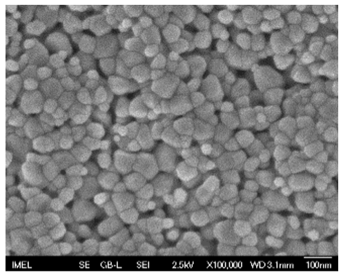 | 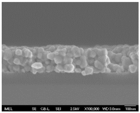 |  | 56 a ± 16 | 217 a ± 8 |
| 2 |  | 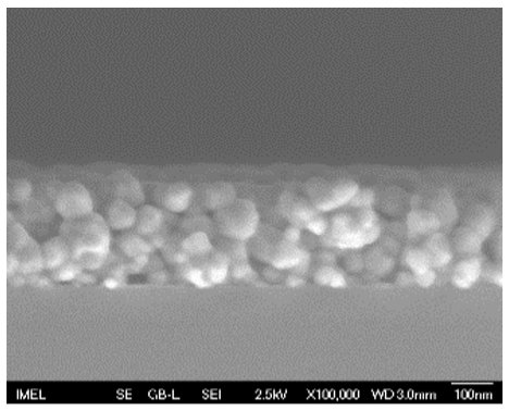 |  | 57 a ± 19 | 247 b ± 10 |
| 3 |  | 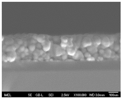 |  | 59 a ± 16 | 268 c ± 10 |
| 4 | 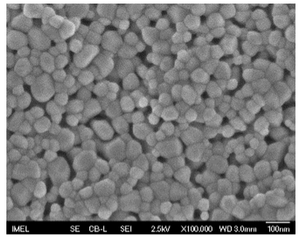 |  | 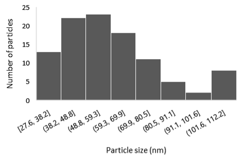 | 60 a ± 20 | 270 c ± 13 |
| 2D Topography | 3D Topography | RMS Roughness sq (nm) | |
|---|---|---|---|
| 1 |  | 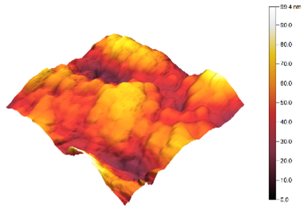 | 12.3 |
| 2 | 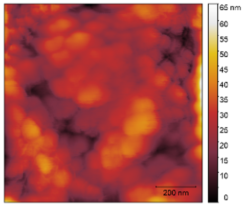 |  | 7.7 |
| 3 | 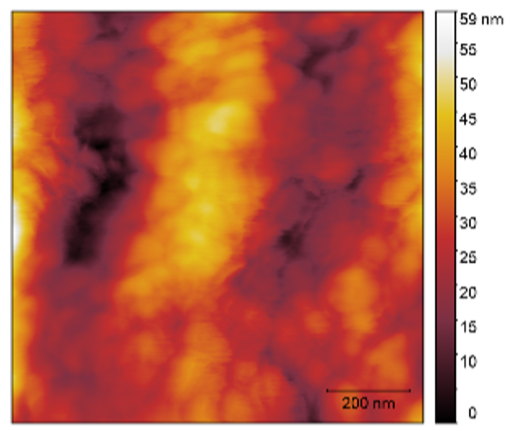 | 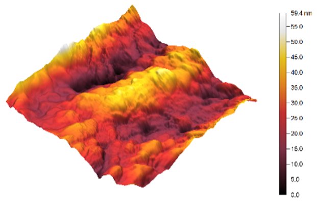 | 9.0 |
| 4 |  | 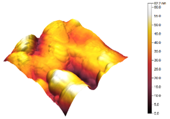 | 9.2 |
| Sensor Response (A)—Time (min) | Sensor Response (A)—CO2 Concentration (ppm) | |
|---|---|---|
| 1 | 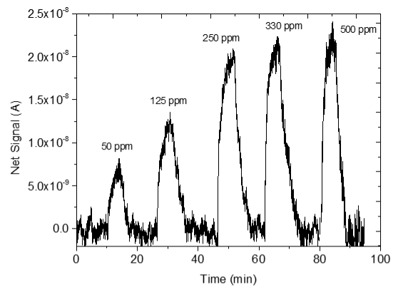 | 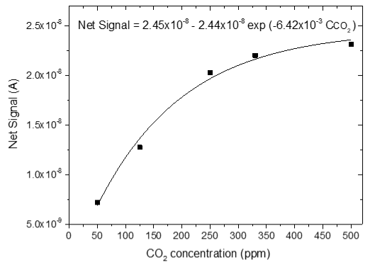 |
| 2 | 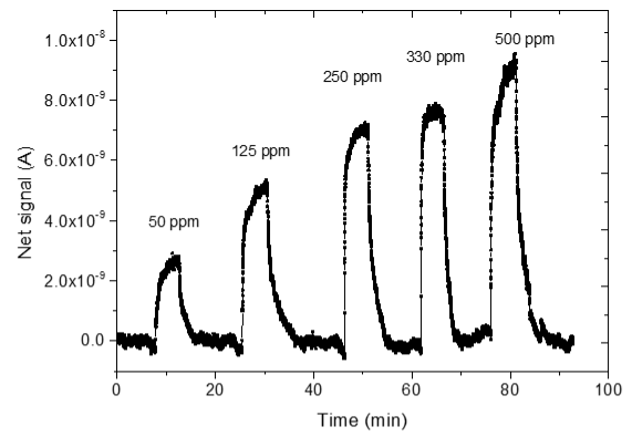 | 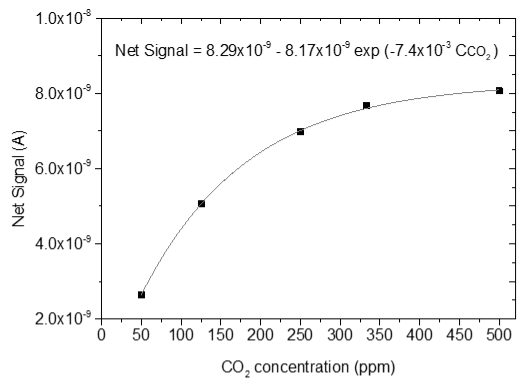 |
| 3 | 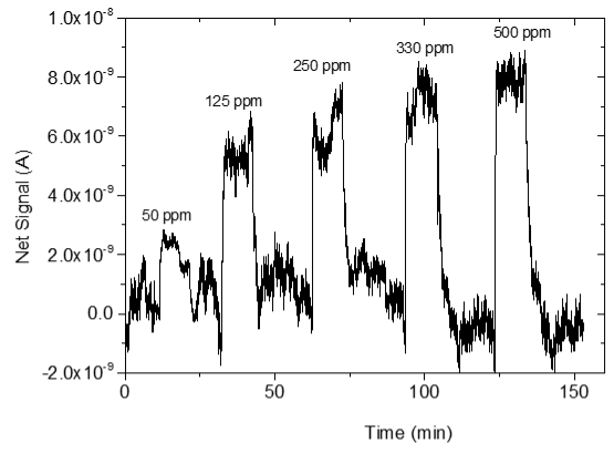 | 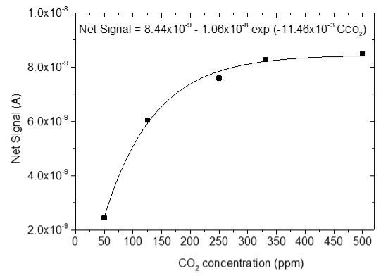 |
| 4 |  |  |
Disclaimer/Publisher’s Note: The statements, opinions and data contained in all publications are solely those of the individual author(s) and contributor(s) and not of MDPI and/or the editor(s). MDPI and/or the editor(s) disclaim responsibility for any injury to people or property resulting from any ideas, methods, instructions or products referred to in the content. |
© 2025 by the authors. Licensee MDPI, Basel, Switzerland. This article is an open access article distributed under the terms and conditions of the Creative Commons Attribution (CC BY) license (https://creativecommons.org/licenses/by/4.0/).
Share and Cite
Stramarkou, M.; Bardakas, A.; Krokida, M.; Tsamis, C. Fabrication of ZnO Thin Films Doped with Na at Different Percentages for Sensing CO2 in Small Quantities at Room Temperature. Sensors 2025, 25, 2705. https://doi.org/10.3390/s25092705
Stramarkou M, Bardakas A, Krokida M, Tsamis C. Fabrication of ZnO Thin Films Doped with Na at Different Percentages for Sensing CO2 in Small Quantities at Room Temperature. Sensors. 2025; 25(9):2705. https://doi.org/10.3390/s25092705
Chicago/Turabian StyleStramarkou, Marina, Achilleas Bardakas, Magdalini Krokida, and Christos Tsamis. 2025. "Fabrication of ZnO Thin Films Doped with Na at Different Percentages for Sensing CO2 in Small Quantities at Room Temperature" Sensors 25, no. 9: 2705. https://doi.org/10.3390/s25092705
APA StyleStramarkou, M., Bardakas, A., Krokida, M., & Tsamis, C. (2025). Fabrication of ZnO Thin Films Doped with Na at Different Percentages for Sensing CO2 in Small Quantities at Room Temperature. Sensors, 25(9), 2705. https://doi.org/10.3390/s25092705