Abstract
This paper proposes a novel high-efficiency isolated three-port bidirectional DC/DC device for photovoltaic (PV) systems. The device contains a high step-up converter for PV modules to supply power to the DC bus, and a bidirectional charge/discharge control circuit for the battery with an improved boost-flyback converter. When the PV modules supply sufficient energy, their output can be stepped up and energy supply to the DC bus and charging of the battery can be achieved simultaneously. However, when the energy supplied is insufficient, the battery provides energy to the DC bus. When the proposed converter is operated in the step-down mode, the DC-blocking capacitor on the high-voltage side is used to reduce the voltage on the transformer and achieve high step-down performance. Moreover, to improve the overall efficiency of the system, the energy stored in the leakage inductance is recycled and supplied to the DC-blocking capacitor during operation in the step-up mode. Finally, to verify the feasibility and practicability of the proposed devices, a 500 W three-port bidirectional DC/DC devices was implemented. The highest efficiencies achieved for operation in different modes were as follows: high step-up mode for the PV modules, 95.2%; battery step-up mode, 94.2%; and step-down mode, 97.6%.
1. Introduction
In recent years, greenhouse gas emissions have increased with advances in technology, leading to global warming and climate change. The energy technology industry continues to be heavily dependent on fossil fuels and is unable to handle this stringent environment [1,2]. Therefore, the use of green energy has become the core of major economic strategies and is a key focus in world politics, especially because reducing greenhouse gas emissions and conserving energy are the main global concerns at present.
In general, because of the large difference between the output voltage of green energy apparatus and the operating voltage of DC bus, a high step-up converter is always required for connecting these two stages. A conventional boost converter should operate with an extremely high duty ratio to provide high step-up voltage. In particular, its maximum step-up ratio is limited by the parasitic elements of the circuit components. The existence of parasitic components [3] and the reverse recovery time of diode [4] reduce the converter efficiency. Consequently, the use of conventional boost converters in the field of green energy is limited. Recently, to achieve a high step-up ratio, the use of a series boost converter, the voltage-lift technique, a coupled inductor, and a cascade circuit structure has been proposed [5,6,7,8,9,10,11]. When the switch of the boost converter is open, a large current flows through the power components, and therefore, power components with high current stress are required, which implies high cost and conduction energy loss. The conventional flyback converter and forward converter have also been proposed for achieving high step-up voltages. However, because the leakage inductance of the transformer in these ones can lead to high reverse voltage across the switch, a passive snubber circuit or an active clamp is required to suppress such a reverse voltage. A passive snubber circuit has a resistance that depletes the excess energy of the leakage inductance, thereby reducing the circuit efficiency. By contrast, an active clamp results in many components being added to the circuit, which not only increases cost but also renders inverter control difficult. In [12], a topology was proposed for solving the leakage inductance problem; however, the remaining disadvantages—large circuit size and high cost—persist.
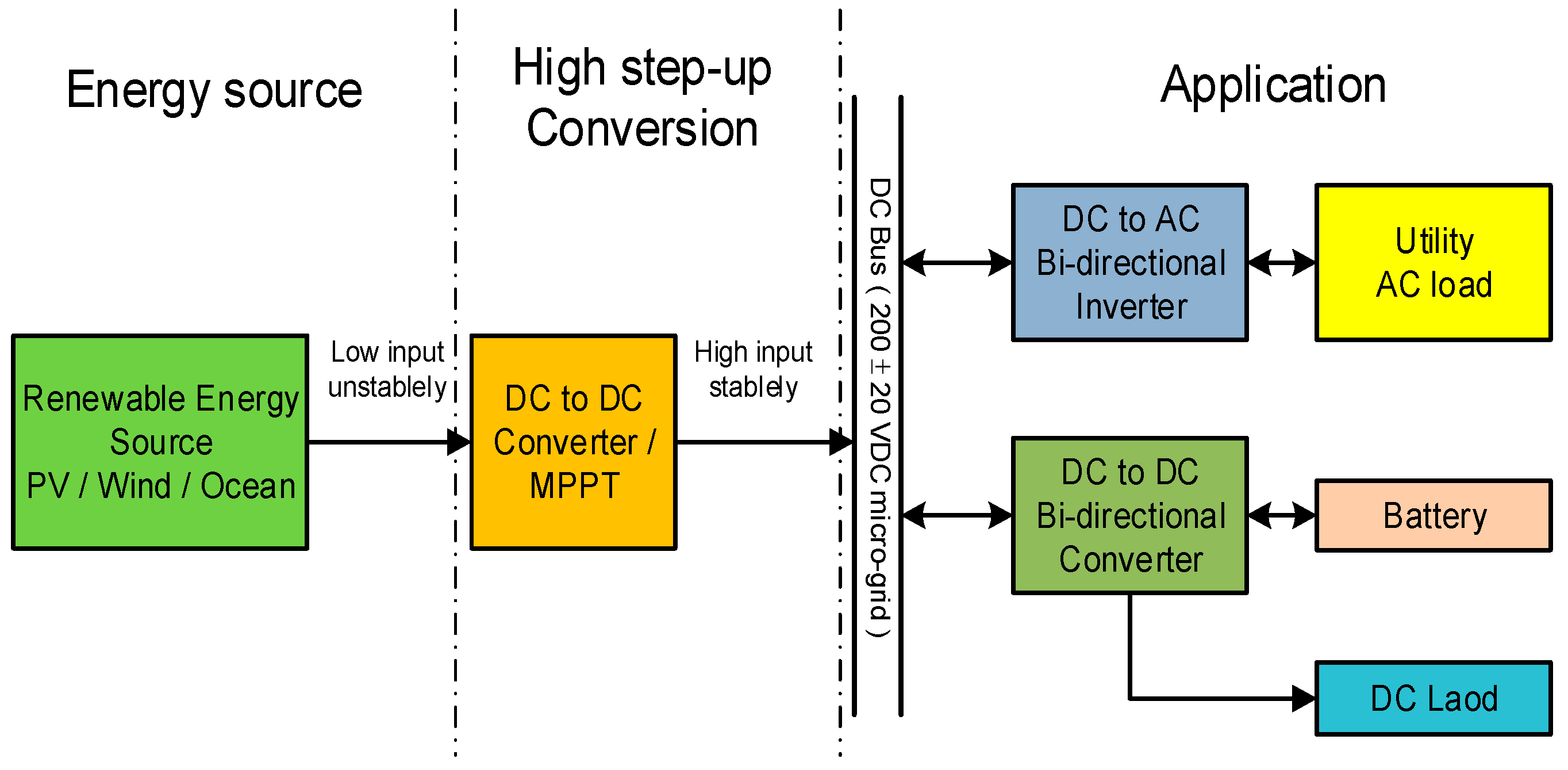
An application block diagram of a typical green energy system is shown in Figure 1. Achieving low cost, a small circuit size, and high efficiency will always be R&D objectives. Furthermore, energy storage systems are a major research subject related to the use of green energy. In the green energy system, because of the large difference between the battery voltage and the DC bus voltage, a high step-up converter is required to transfer energy from the battery to the DC bus. Recently, many studies have conducted research on bidirectional converters [13,14,15,16,17,18,19,20,21,22,23,24,25]. They have attempted to develop a topology that can provide both step-up and step-down operations; which has the potential to reduce the number of components, cost, and size of the system. The commonly used non-isolated bidirectional devices, including the buck/boost bidirectional devices [13], bidirectional Cuk devices [14], and bidirectional single-ended primary inductance devices (SEPIC) [15], have few components, low cost, and high controllability; moreover, they are easy to design. However, all of them have low efficiency and can become unstable when operating at a high voltage conversion rate [3]. Furthermore, these non-isolated circuits are susceptible to interference and cannot be used to achieve electricity isolation, factors that considerably limit their use. While the commonly used isolated bidirectional converters are full-bridge bidirectional converters [17,26,27], half-bridge bidirectional converters [19], and bidirectional flyback converters [18]. Both full-bridge and half-bridge bidirectional converters can perform soft switching by controlling the phase shift, resulting in high efficiency, but their transformer design is such that achieving inductance–inductance–capacitance (IIC) resonance is difficult. Furthermore, bidirectional flyback converters have the same advantages as non-isolated bidirectional converters: few components, low cost, and ease of design. When its switch is OFF, the leakage inductor of the transformer and the parasitic capacitor in the switch produce resonance, resulting in a voltage spike at the switch; therefore, a switch with high voltage stress is required. The aforementioned isolated bidirectional converters always have a large transformer because a high turns ratio is necessary for operation at a high voltage conversion rate. Recently, many modified bidirectional converters have been proposed. For example, Reference [21] shows a bidirectional converter that can recycle the energy of the leakage inductor of the transformer and perform synchronous rectification; thus, the converter shows high efficiency while meeting the requirement of electricity isolation. However, the converter topology involves two inductors, and the transformer is considered an ideal transformer despite having a low turns ratio; moreover, the energy release problem associated with the magnetizing inductor leads to low efficiency for high-power operations. Reference [22] proposed that the battery, which is the auxiliary power source, should be charged and used for providing energy to the DC bus during circuit operation in the step-up mode. The leakage inductance of the coupled inductor can recycle the energy and release it to the battery auxiliary power circuit and DC bus on the high-voltage side. However, the circuit control procedure is complicated, and the battery auxiliary power cannot supply energy to the DC bus.
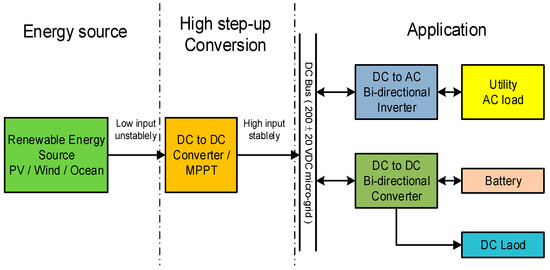
Figure 1.
Application block diagram of a green energy system.
Although a bidirectional converter provides both step-up and step-down voltages, when it is used in a photovoltaic (PV) system, energy generated by the PV system is required to pass through two converter stages for charging the battery, resulting in a reduction in the overall efficiency of the system. To overcome this problem, a three-port DC/DC converter topology has been proposed [23,24,25,26,27,28,29,30,31,32,33,34] for the PV system. When the energy supplied by the PV modules is sufficient, supply of energy to the DC bus and charging of the battery are simultaneously performed. However, in the absence of energy supply from the PV modules, the battery can provide energy to the DC bus. The three-port DC/DC converter can operate in different modes, thereby reducing the cost and size of the system [26,27,28,29,30,31,32,33]. However, it has a larger size, higher cost, and lower efficiency compared with the converter proposed in the current study. In general, a three-port DC/DC converter is not involved in the charging of the battery by the DC bus. This implies that the converter lacks the step-down mode, similar to bidirectional converters. If a topology could combine the advantages of both bidirectional converters and the three-port converter, the size and cost of the system could be further reduced.
For the reasons mentioned above, in this paper we propose a novel isolated three-port bidirectional DC/DC converter whose block diagram is shown in Figure 2. When the energy supplied by the PV modules is sufficient, the converter can not only step up the output of the PV modules, but also provide energy to the DC bus and charge the battery simultaneously. However, when the energy supplied is insufficient, the converter can step up the output of the battery and provide energy to the DC bus. Any excess energy in the DC bus is used to charge the battery, implying that the proposed topology can perform both high step-up and high step-down functions. The topology proposed is isolated, and the DC -blocking capacitor on the high-voltage side can reduce the voltage on the transformer, facilitating the operation of the system in the high step-down mode. An improved boost-flyback converter is used on the low-voltage side of the PV modules to step up the output of the PV modules for charging the battery and providing energy to the DC bus. The auxiliary inductor on the battery side can modify the output step-up voltage and provide a continuous current for battery charging, which can extend the battery lifetime. Additional switches and diodes are added to prevent the energy generated by the PV system from directly flowing to the battery and to control the step-up process for providing energy to the DC bus in the absence of energy supply from the PV system. The proposed topology consists of three operational modes, which reduce the cost and size of the system considerably. Furthermore, the converter can perform synchronous rectification and recycle energy from the leakage inductor simultaneously, and these functions increase the overall efficiency of the system considerably.
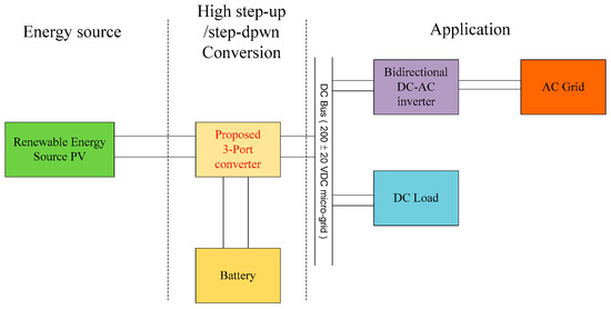
Figure 2.
Block diagram of a three-port bidirectional converter.
2. Operating Principles of the Main Circuit
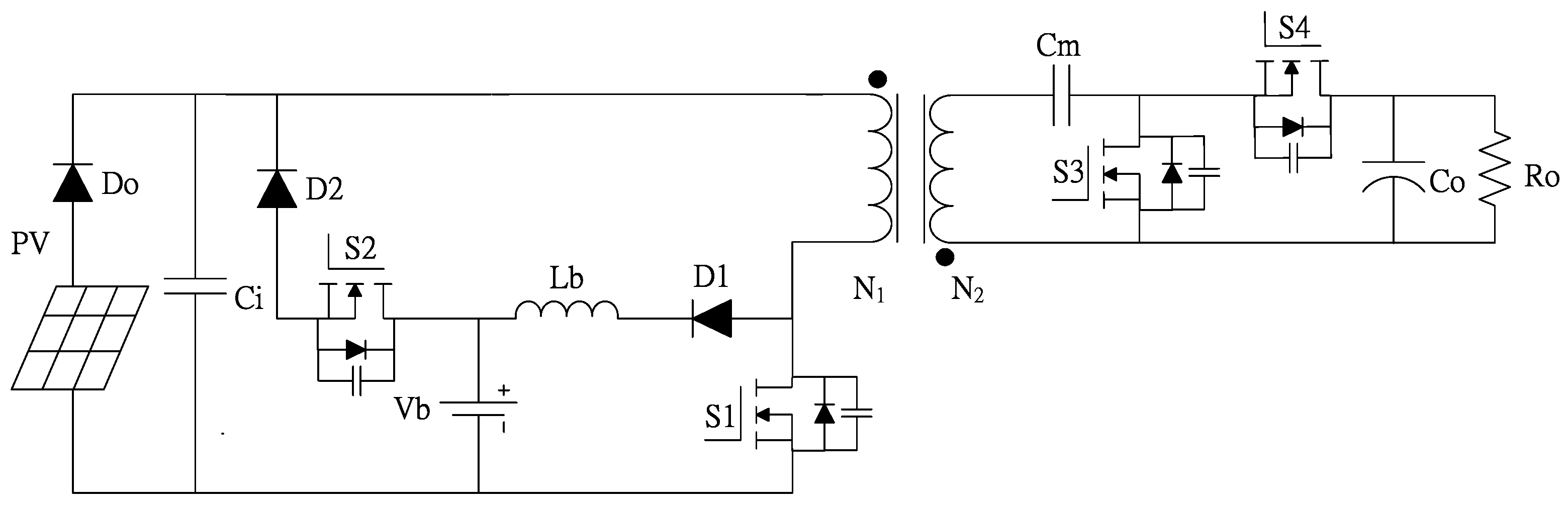
The detailed scheme of our proposed device is shown in Figure 3 and briefly discussed in this section. The DC-blocking capacitor Cm on the high-voltage side facilitates the operation of the system in the high step-down mode by reducing the voltage on the transformer. It can also recycle the energy of the leakage inductor on the secondary side of the transformer and increase the efficiency of the system. An improved boost-flyback converter is used on the low-voltage side of the PV modules to step up the output of the PV modules for charging the battery and providing energy to the DC bus. The auxiliary inductor Lb on the battery side can modify the stepped-up output voltage for providing a continuous current for charging the battery. Switch S2 and diode D2 not only prevent the energy generated by the PV system from directly charging the battery, but also control the step-up process for providing energy to the DC bus and charging the battery when the energy supplied by the PV modules is sufficient. In the absence of energy supply from the PV modules, the battery output is stepped up and energy is provided to the DC bus. Any excess energy in the DC bus is used to charge the battery.
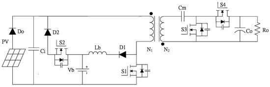
Figure 3.
Novel isolated three-port bidirectional DC/DC converter.
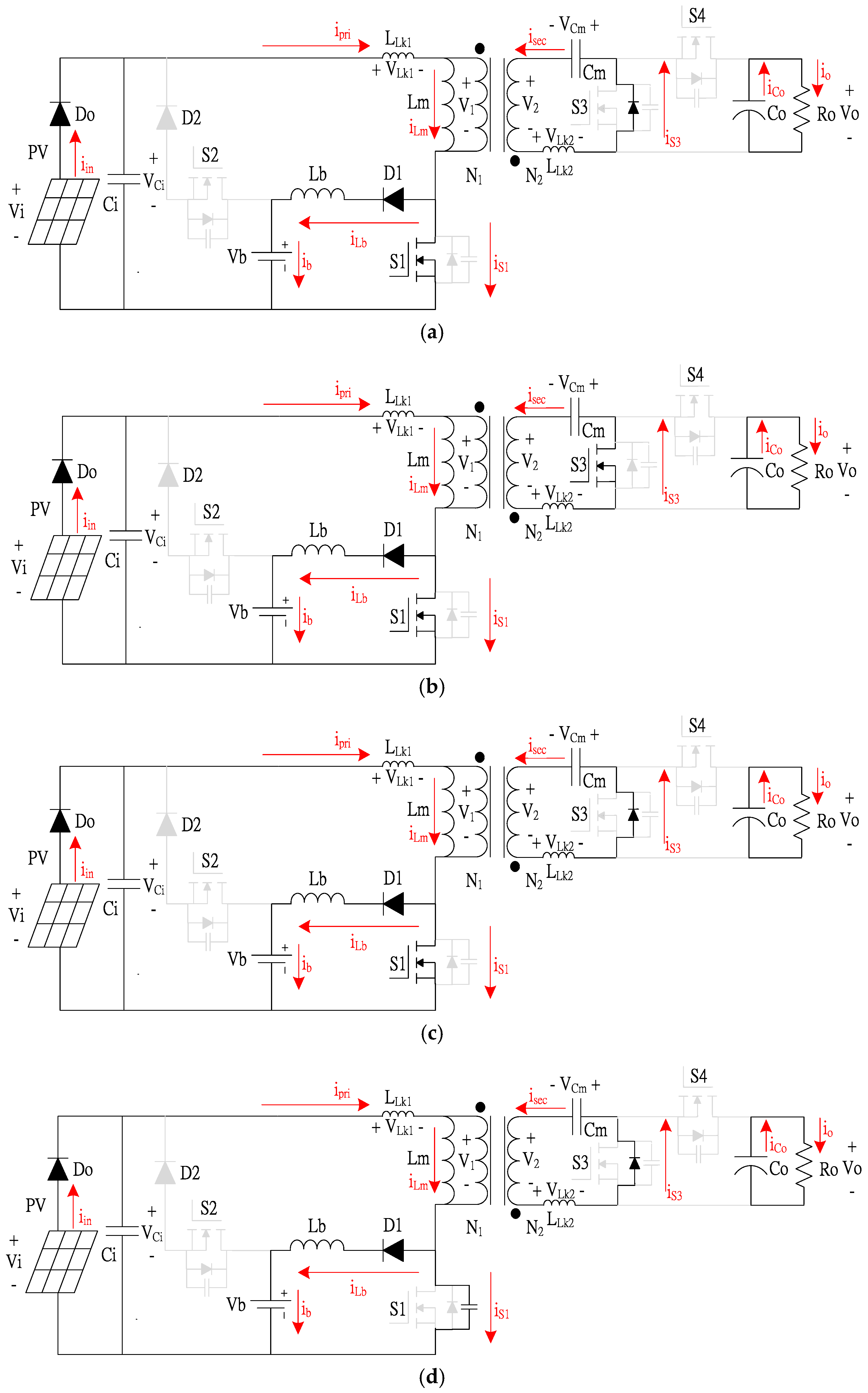
The proposed topology was studied and analyzed by considering three operation stages. In Stage 1, the output of PV modules is stepped up for charging the battery and providing energy to the DC bus when the energy supplied by the PV modules is sufficient. In Stage 2, the output of the battery is stepped up to provide energy to the DC bus when the energy supplied by the PV modules is insufficient. In Stage 3, the output of the DC bus is stepped down and the battery is charged when there is excess energy in the DC bus. To simplify the analysis of the converter, the following assumptions were made:
- (1)
- Capacitors Ci and Co have very high capacitance and can be considered as current sources.
- (2)
- Switches S1, S2, S3, and S4 and diodes D1 and D2 are considered as ideal components.
- (3)
- The magnetizing inductances of the transformer are larger than the leakage inductances of the transformer.
2.1. Stage 1: Stepping up the PV Output for Providing Energy to The DC Bus and Charging the Battery
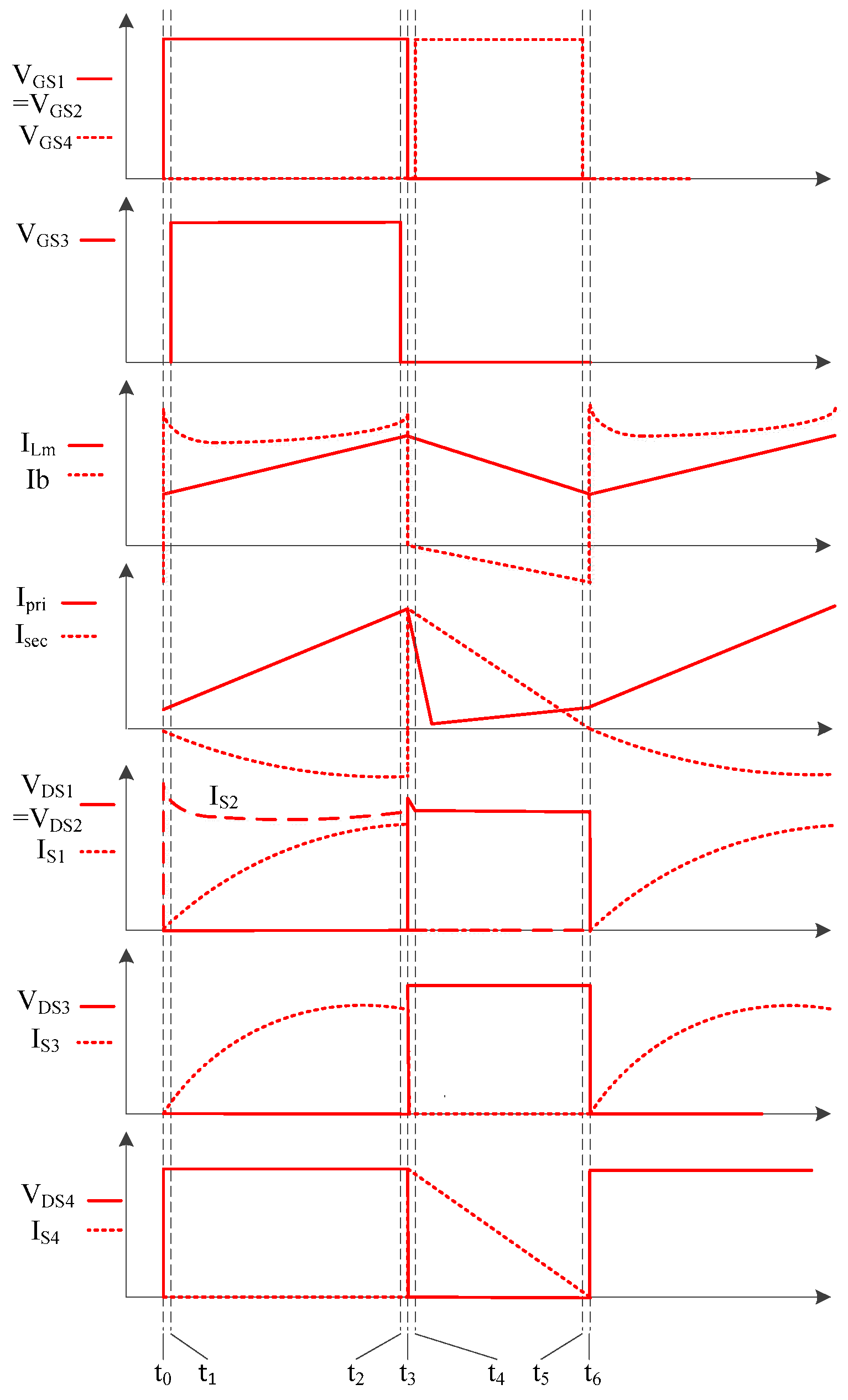
The output voltage of the PV modules is stepped up before being supplied to the DC bus and battery. The waveforms of the main components operating in Stage 1 are shown in Figure 4, and the operating principle is as shown in Table 1.
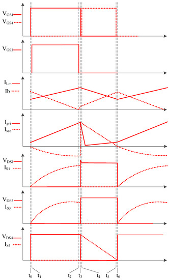
Figure 4.
Key waveforms in Stage 1.

Table 1.
Operating principle of Stage 1.
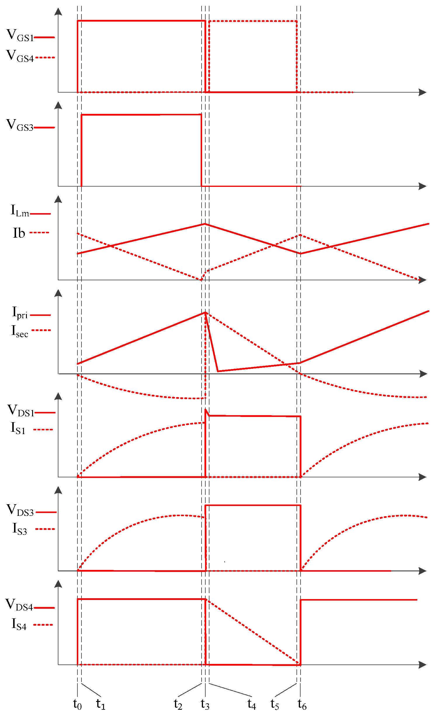
2.2. Stage 2: Stepping up the Battery Output
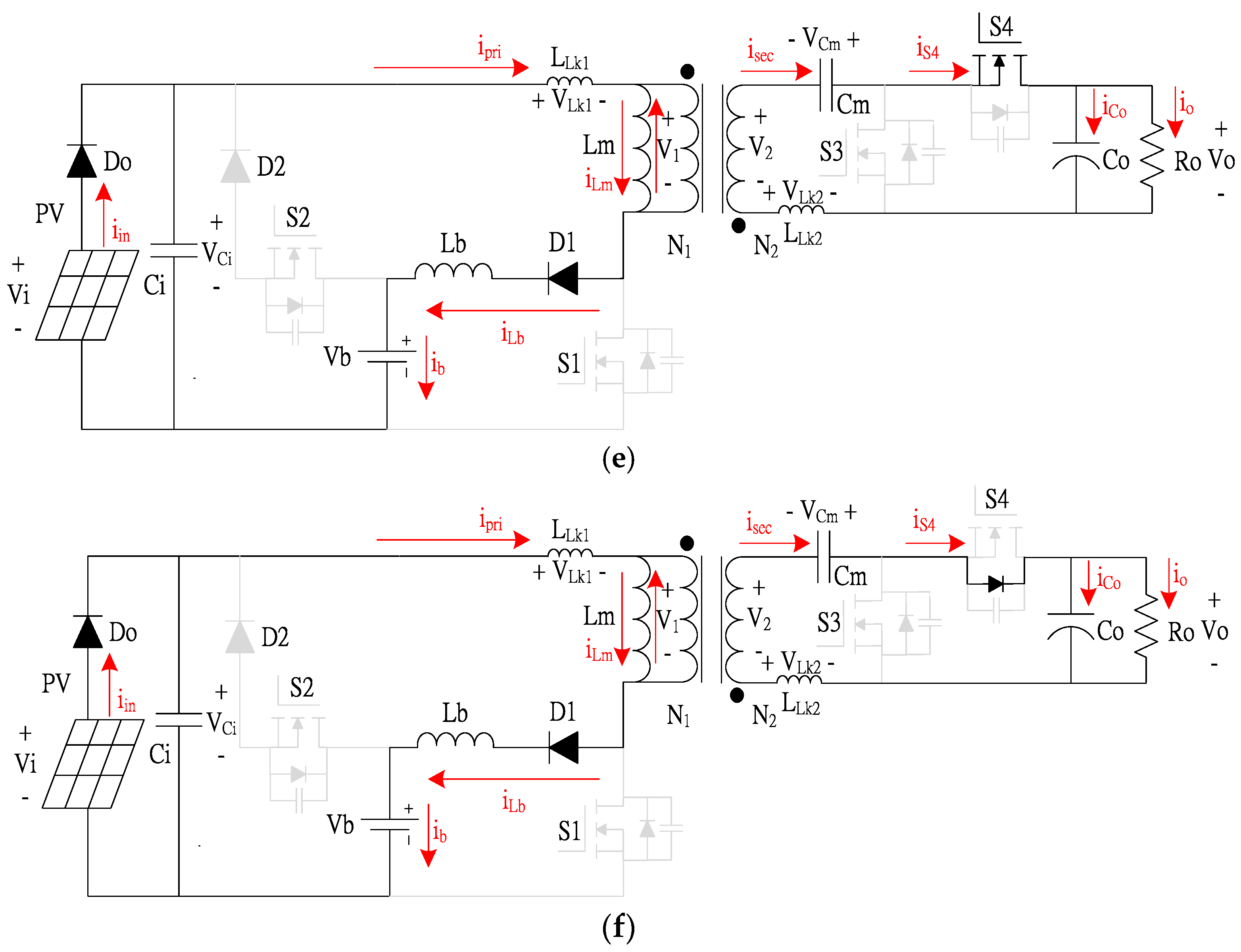
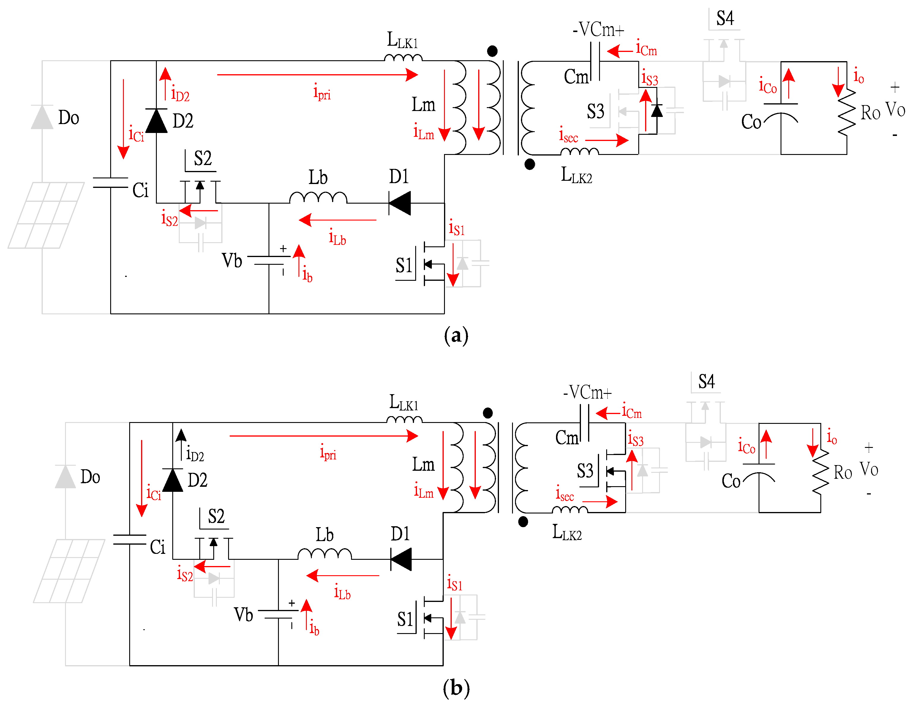
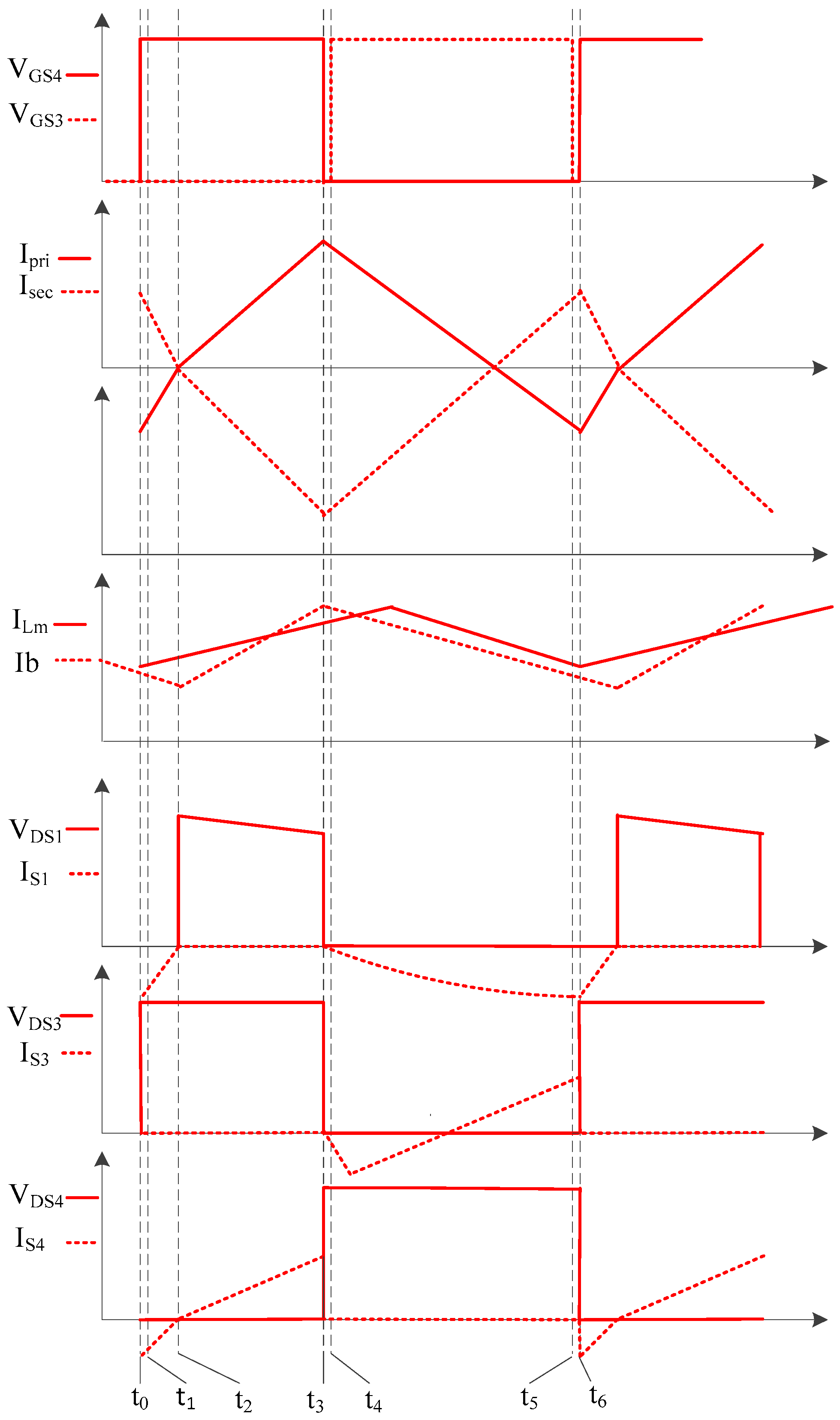
In Stage 2, the output voltage of the battery is stepped up to provide energy for the DC bus. Figure 6 shows the key waveforms of the main components operating in this stage, and the operating principle is as shown in Table 2.
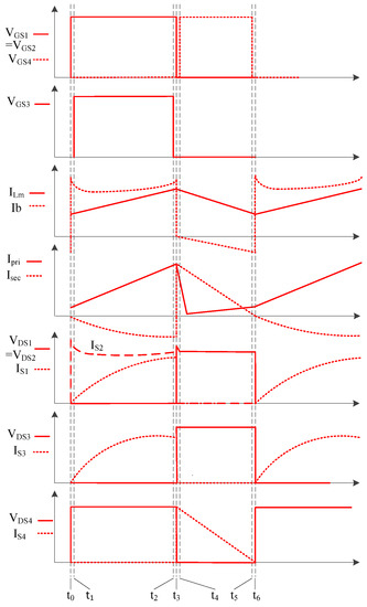
Figure 6.
Key waveforms in Stage 2.
Table 2.
Operating principle of Stage 2.
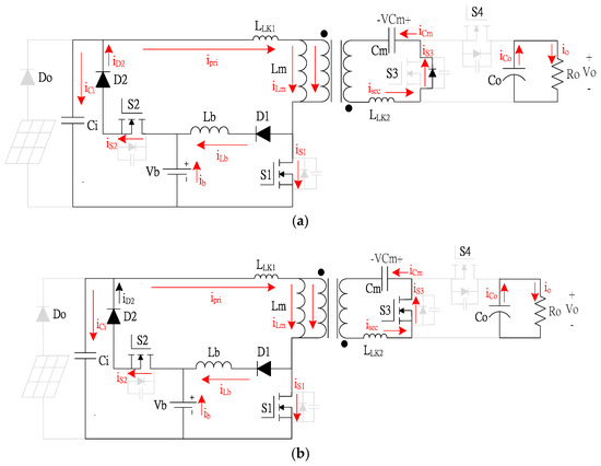
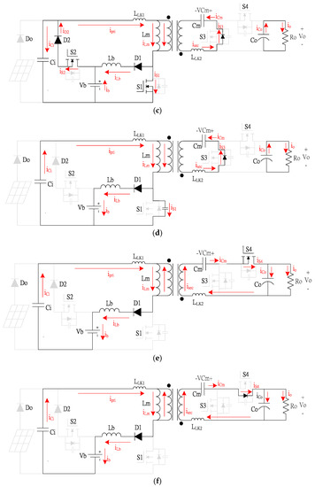
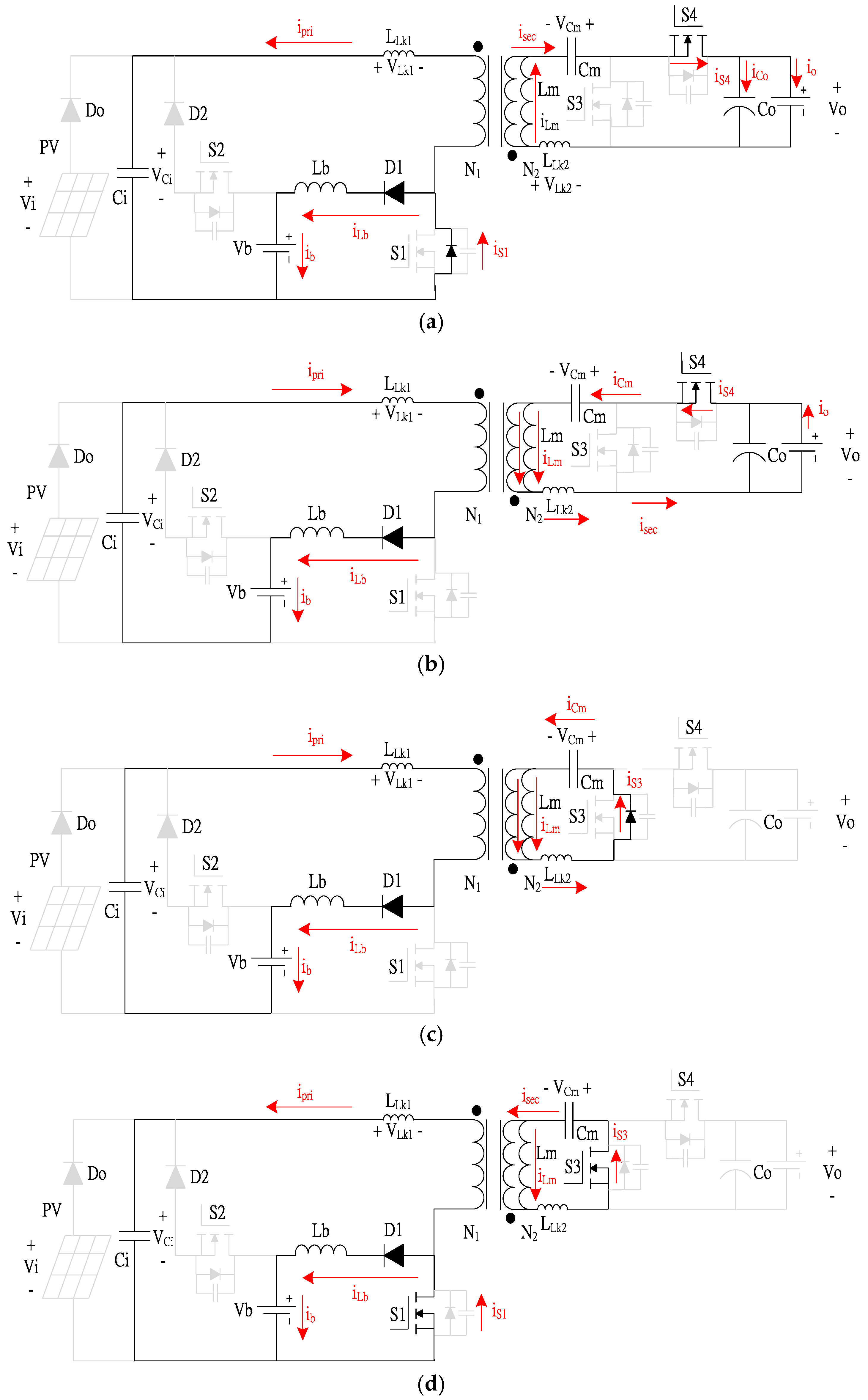
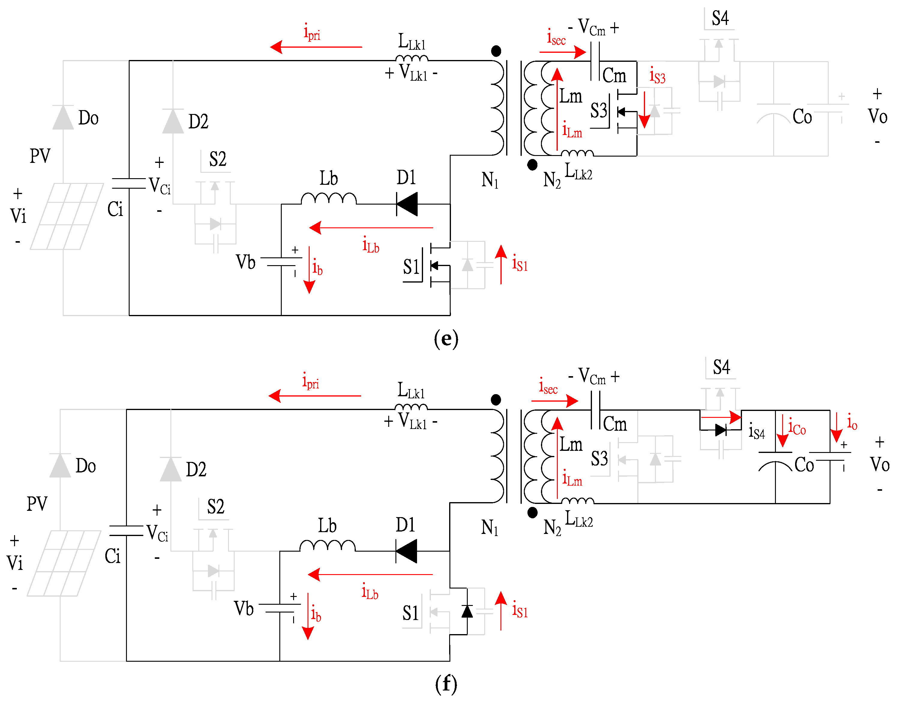
Figure 7.
Operating diagram of each mode in Stage 2: (a) Mode I; (b) Mode II; (c) Mode III; (d) Mode IV; (e) Mode V; and (f) Mode VI.
2.3. Stage 3: Stepping Down the Output of the DC Bus
When the energy supplied by the PV modules is insufficient, the system steps down the output voltage of the DC bus for battery charging. The key waveforms of the proposed converter topology in this stage are shown in Figure 8, and the operating principle is as shown in Table 3.
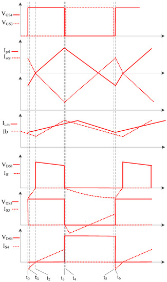
Figure 8.
Key waveforms in Stage 3.
Table 3.
Operating principle of Stage 3.
3. Steady-State Analysis
This section focuses on the mathematical derivation of the voltage conversion ratio and the voltage stress of components. The following assumptions were made to simplify the analysis:
- (1)
- Capacitors Ci and Co have very high capacitance and can be considered as current sources;
- (2)
- Switches S1, S2, S3, and S4 and diodes D1 and D2 are considered as ideal components;
- (3)
- The leakage inductances of the transformer are smaller than the magnetizing inductances, and therefore, they can be neglected;
- (4)
- The system operates in the continuous conduction mode.
3.1. Voltage Conversion Ratio
When the energy supplied by the PV modules is sufficient, switch S1 is turned ON and the voltage difference across the magnetizing inductor is equal to the input voltage of the PV modules. In the absence of energy supplied by the PV modules, switches S1 and S2 are turned ON and the voltage across the magnetizing inductor is equal to the battery voltage. Because the input voltage of the PV modules and the battery voltage are almost the same in a three-port converter, both step-up from the PV modules to the DC bus and that from the battery to the DC bus have the same step-up ratio. To simplify the derivation of the voltage conversion ratio, first, we neglect part of the battery circuit.
(1) Step-up voltage conversion ratio GVo
When switch S1 is turned on:
where it is assumed that N = and the total turn-on time Ton = DTs.
When switch S1 is turned OFF:
Substituting (3) into (4) gives:
The total turn-off time Toff is given by (1 − D)Ts.
According to the principle of voltage-second balance:
Assuming that all the energy of the magnetizing inductors is transferred to the battery and that the maximum current is equal to the current of the magnetizing inductors, we can design the battery charging current:
(2) Step-down voltage conversion ratio GVb
For deriving the step-down voltage conversion ratio of the DC bus, which charges the battery, switch S2 and diode D2 should first be turned OFF, and subsequently, switch S4 is turned ON and switch S3 is turned OFF:
VLm = (Vo − VCm)
When switch S4 is turned OFF and switch S3 is turned ON, we have:
Substituting (11) into (14) gives:
According to the principle of voltage-second balance:
3.2. Voltage Stress of Components
The voltage stress of each component can be derived by analyzing its operation in the ON and OFF states. The voltage stress of switch S1 in the ON state can be determined using Figure 5a:
Vi − VLm = 0
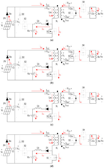
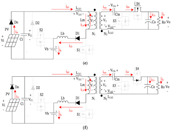
Figure 5.
Operational diagram of each mode in Stage 1: (a) Mode I; (b) Mode II; (c) Mode III; (d) Mode IV; (e) Mode V; and (f) Mode VI.
On the basis of voltage-second balance, VLmDTS + VLm(1 − D)TS = 0. Therefore, we can derive the voltage stress of switch S1 to be:
Because diode D2 is considered ideal, the voltage of switch S2 is equal to the difference between the battery voltage and the voltage across the input capacitor:
VS2 = VB − VCi
In the step-down mode, when switch S4 is turned ON, switch S3 is turned OFF, as shown in Figure 9e, and the voltage across S3 is equal to the output voltage:
VS3 = Vo
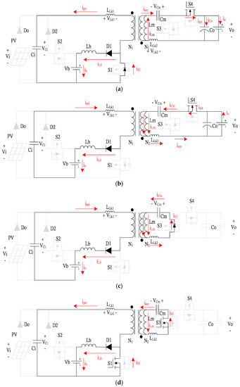
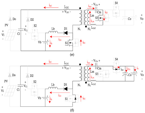
Figure 9.
Operating diagram of each mode in Stage 3: (a) Mode I; (b) Mode II; (c) Mode III; (d) Mode IV; (e) Mode V; and (f) Mode VI.
In the step-down mode, when switch S3 is turned ON, switch S4 is turned OFF, as shown in Figure 9b, and the voltage across S4 is equal to the output voltage:
VS4 = Vo
When the entire energy stored in Lb is released and switch S1 is turned ON, diode D1 is turned OFF, and the voltage difference across the diode equals the battery voltage:
VD1 = VB
Diode D2 has the same voltage stress as switch S2 does:
VD2 = VB − VCi
When switch S3 is turned ON in the step-down mode, the voltage stress on the input capacitor Ci is:
The voltage stress of output capacitor Co is equal to Vo:
VCo = Vo.
The voltage stress of voltage-doubling capacitor Cm can be expressed as:
VCm = Vo/2
4. Experimental Results and Analysis
In this section, a comparison between the proposed converter and two groups of converters is presented. First, we compare the proposed converter with the bidirectional converters presented in [21,22]. As shown in Table 4, the converters presented in [21,22] can be used only as traditional bidirectional converters, whereas the proposed three-port bidirectional converter can operate in three stages and perform different functions. Apart from regular bidirectional step-up/step-down operations, the proposed converter can be used in a PV system as a three-port converter. Although the converter presented in [21] does not require a diode and has a lower turns ratio of the transformer, it has one more inductor, resulting in a larger system size. Furthermore, the efficiency of the converter presented in [21] decreases during high-power operations, and the maximum power at which the converter can be operated is 200 W. Although the converter presented in [22] can operate at 1 kW, its efficiency does not reach even 90% for operation above 500 W. In addition, controlling the switches is considerably complicated.
Table 4.
Comparison of the Proposed Converter with Existing Bidirectional Converters.
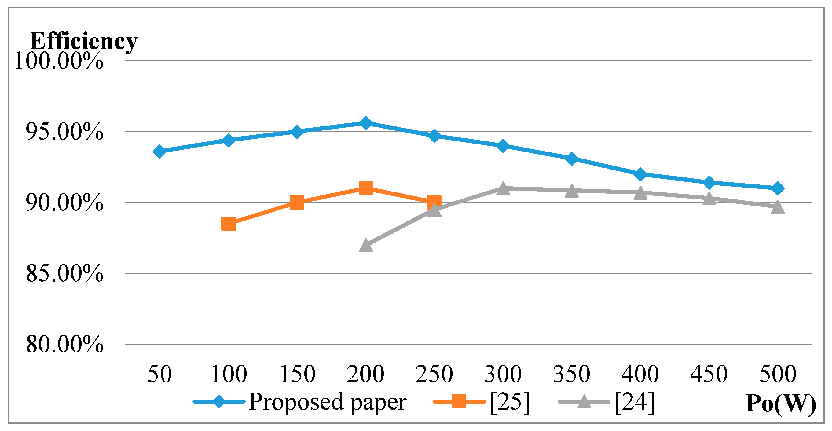
Table 5 presents a comparison between the proposed converter and the converters proposed in [24,25]; all of them are three-port converters. In the table, the highest conversion efficiency is the calculated efficiency of energy conversion from the PV modules to the DC bus, and the proposed converter is superior in conversion efficiency. In addition, the proposed converter has a higher step-up ratio, fewer components, and lower cost. The converter proposed in [24] requires two transformers and an inductor on the output side, and therefore, it is a larger and costlier system; moreover, it cannot achieve high efficiency in high-power operations, and its maximum efficiency is approximately 90.9%. Although the converter proposed in [25] has lower cost compared with that presented in [24], it is not superior in efficiency and system size. Moreover, its step-up ratio cannot be increased by a factor of ten despite the turns ratio of the transformer being identical to that of the proposed converter topology. Additionally, because there is no inductor on the output side, the converter proposed in [25] has low efficiency in high-power operations. Typically, a three-port converter cannot charge a battery by using energy from the DC bus, but the proposed converter has this capability; therefore, the proposed converter is more suitable for PV systems.
Table 5.
Comparison of the Proposed Converter with Other Three-Port Converter.
To verify the operation of the proposed isolated bidirectional three-port DC/DC converter, a 500 W hardware prototype was designed and implemented (Figure 10). The microcontroller unit dsPIC30F4011 was used as the control unit for the proposed converter topology, and the performance was measured for a light load of 50 W, half load of 250 W, and full load of 500 W. The measured waveforms of all components confirmed the feasibility and practicability of the proposed converter topology. The specifications and component parameters are presented in Table 6.
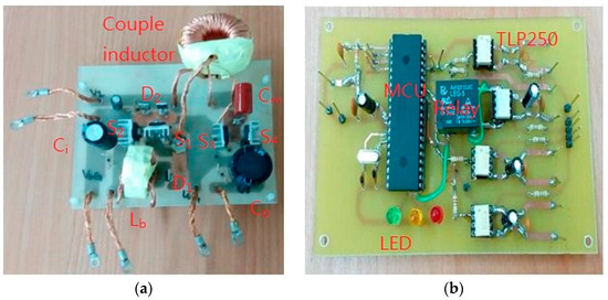
Figure 10.
Photographs of the proposed three-port bidirectional DC/DC converter: (a) the converter circuit and (b) the control circuit.
Table 6.
Electrical Specifications and Component Parameters of the Proposed Converter.
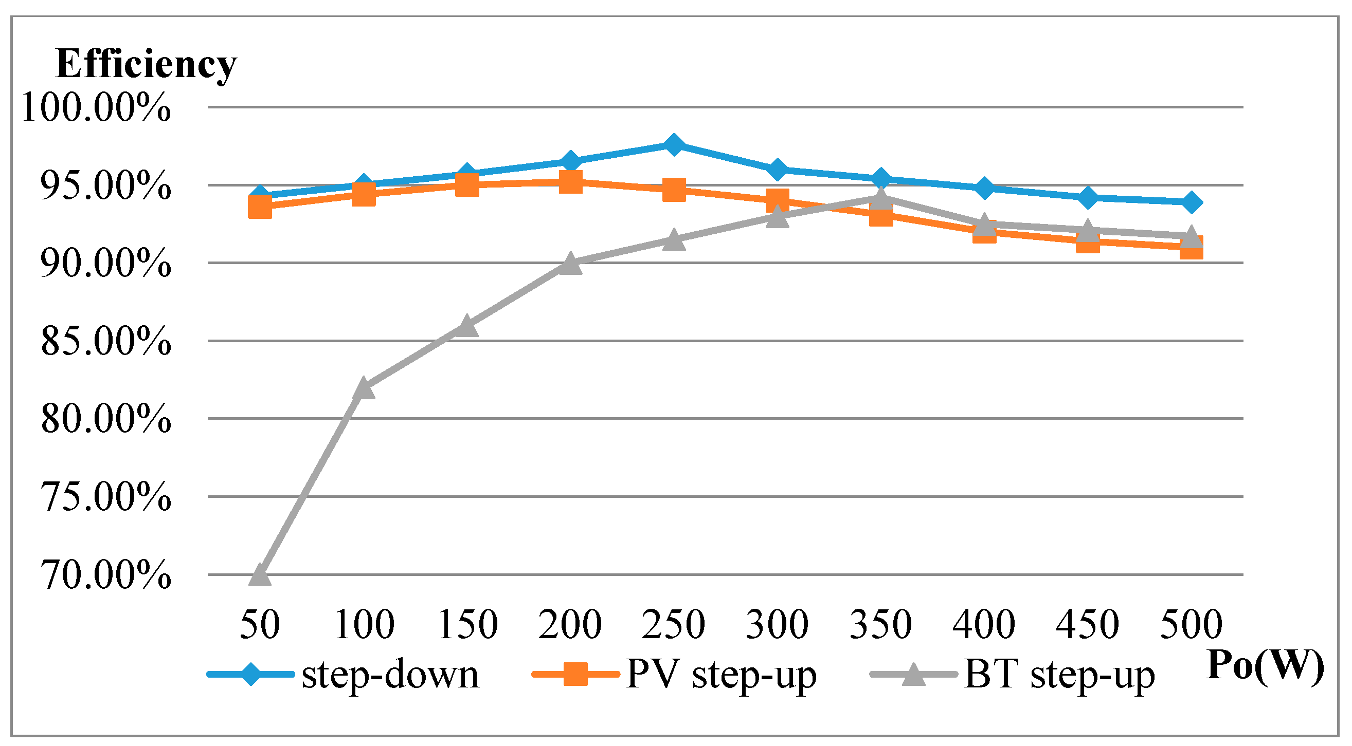
Figure 11 shows the measured efficiency curves of the proposed converter topology for operation in the three stages. The efficiencies corresponding to operations with the light load and full load in Stage 1 are 92% and 91%, respectively. However, for operation at approximately 200 W, the highest efficiency is 95.2%. Furthermore, for Stage 2, the highest efficiency is 94.2%. Finally, for Stage 3, the efficiencies for the light load and full load are 94.3% and 93.9%, respectively. For operation at 250 W, the highest efficiency reached was 97.6%.
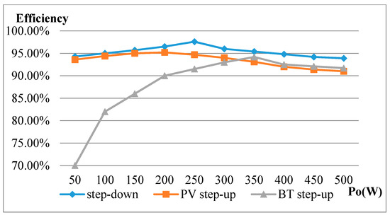
Figure 11.
Efficiency curves of the proposed three-port bidirectional converter.
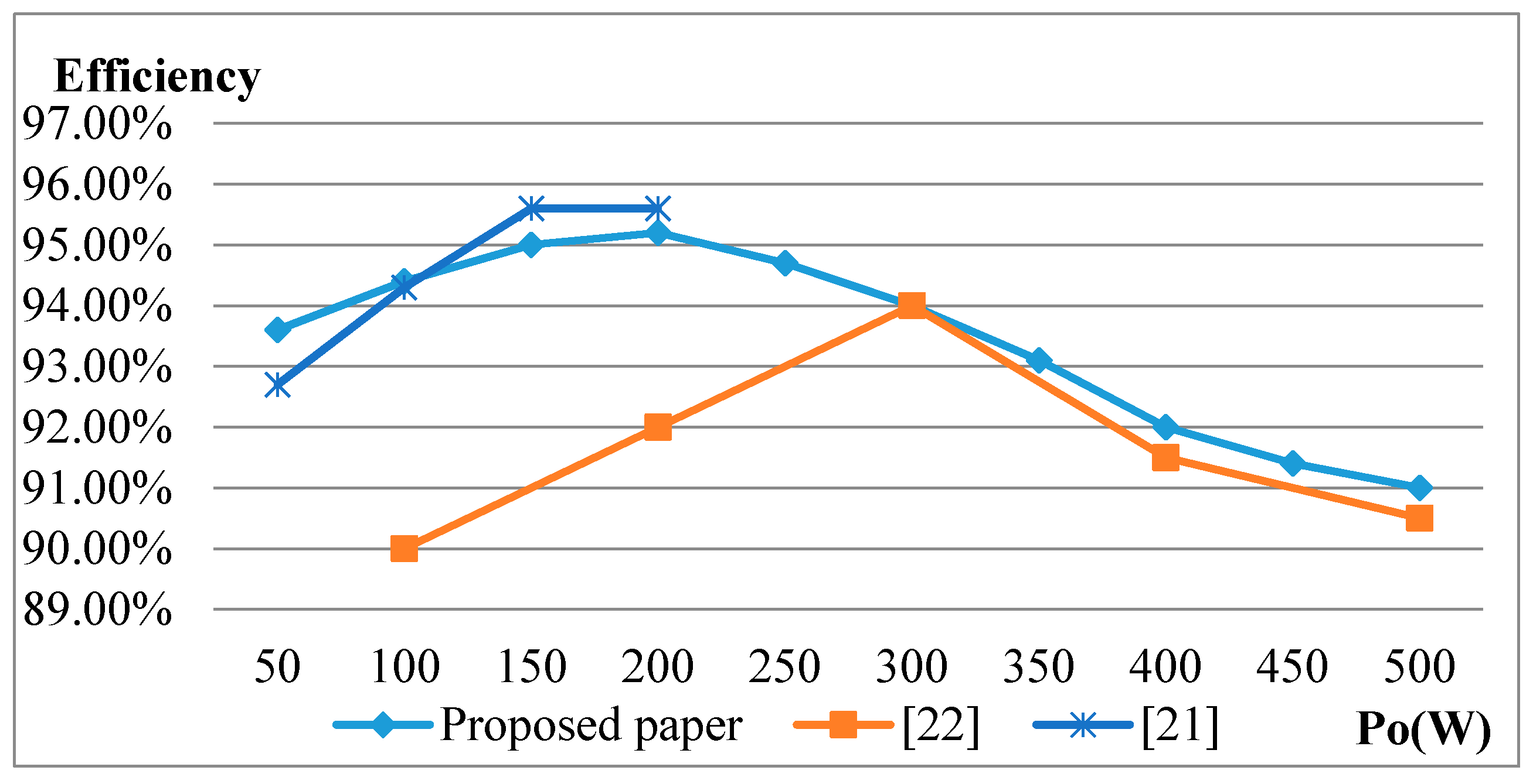
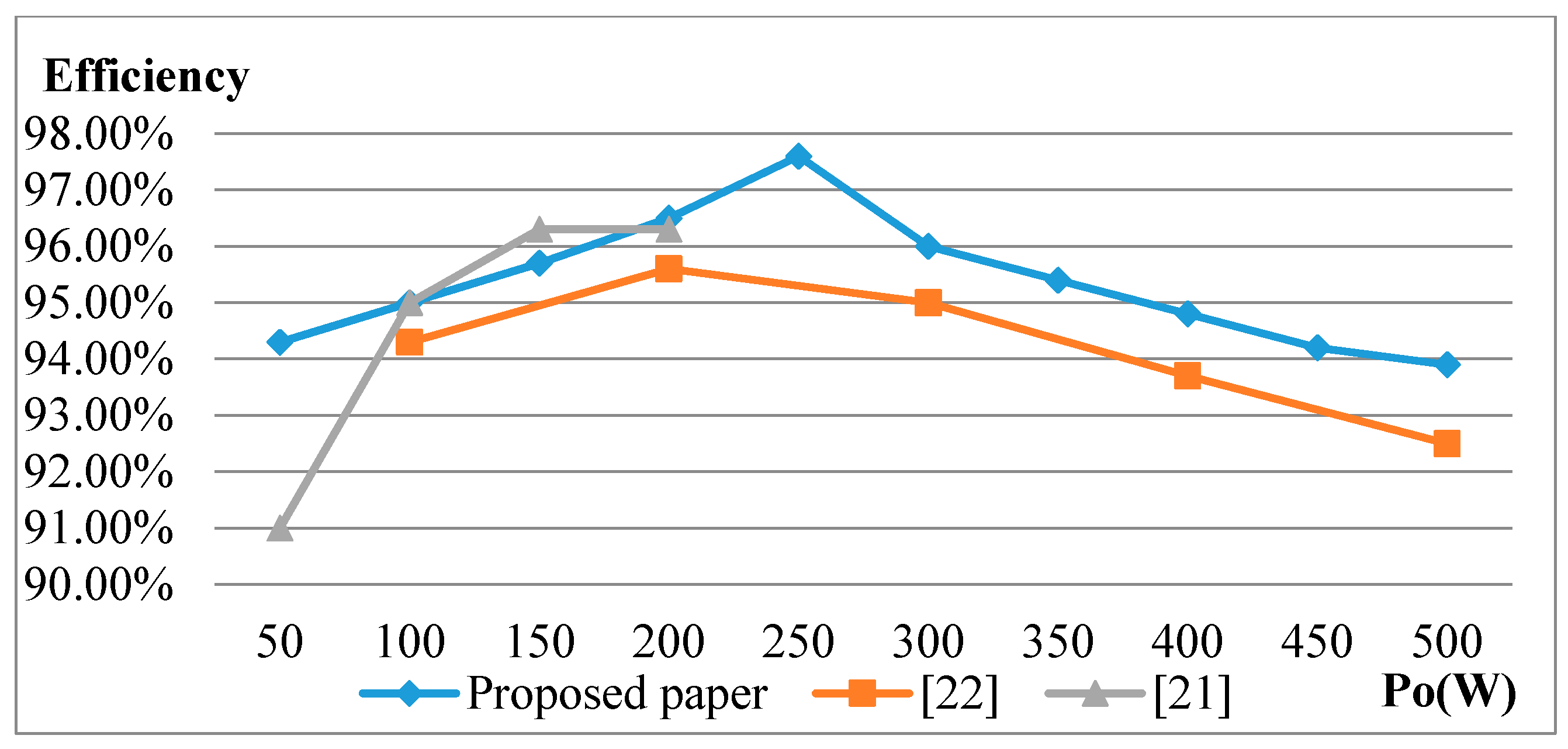
Figure 12 shows a comparison graph of the measured step-up efficiencies of the proposed converter and the converters proposed in [21,22]. Although the efficiency of the proposed converter is greater than that of the converter proposed in [22], it is lower than the efficiency of the converter presented in [21]. In particular, the proposed converter can operate in three stages and at higher powers. Figure 13 shows another comparison graph of the proposed converter and the converters presented in [21,22] for operation in the step-down mode. Clearly, the proposed converter shows higher step-down efficiency.
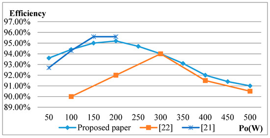
Figure 12.
Comparison graphs of the measured efficiencies of the proposed converter and existing bidirectional converters for operation in the step-up mode.
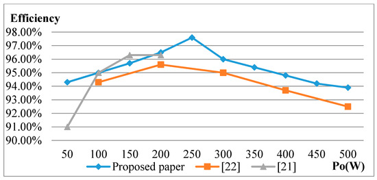
Figure 13.
Comparison graphs of measured efficiencies of the proposed converter and existing bidirectional converters for operation in the step-down mode.
Figure 14 shows a comparison graph of the efficiencies of the proposed converter topology and the converter topologies presented in [24,25] for operation in Stage 1. Clearly, the proposed converter topology is superior.
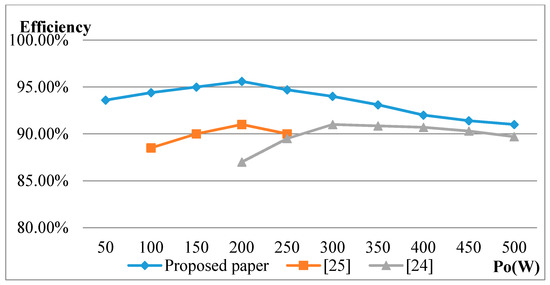
Figure 14.
Comparison graphs of the measured efficiencies of the proposed converter and other three-port converters.
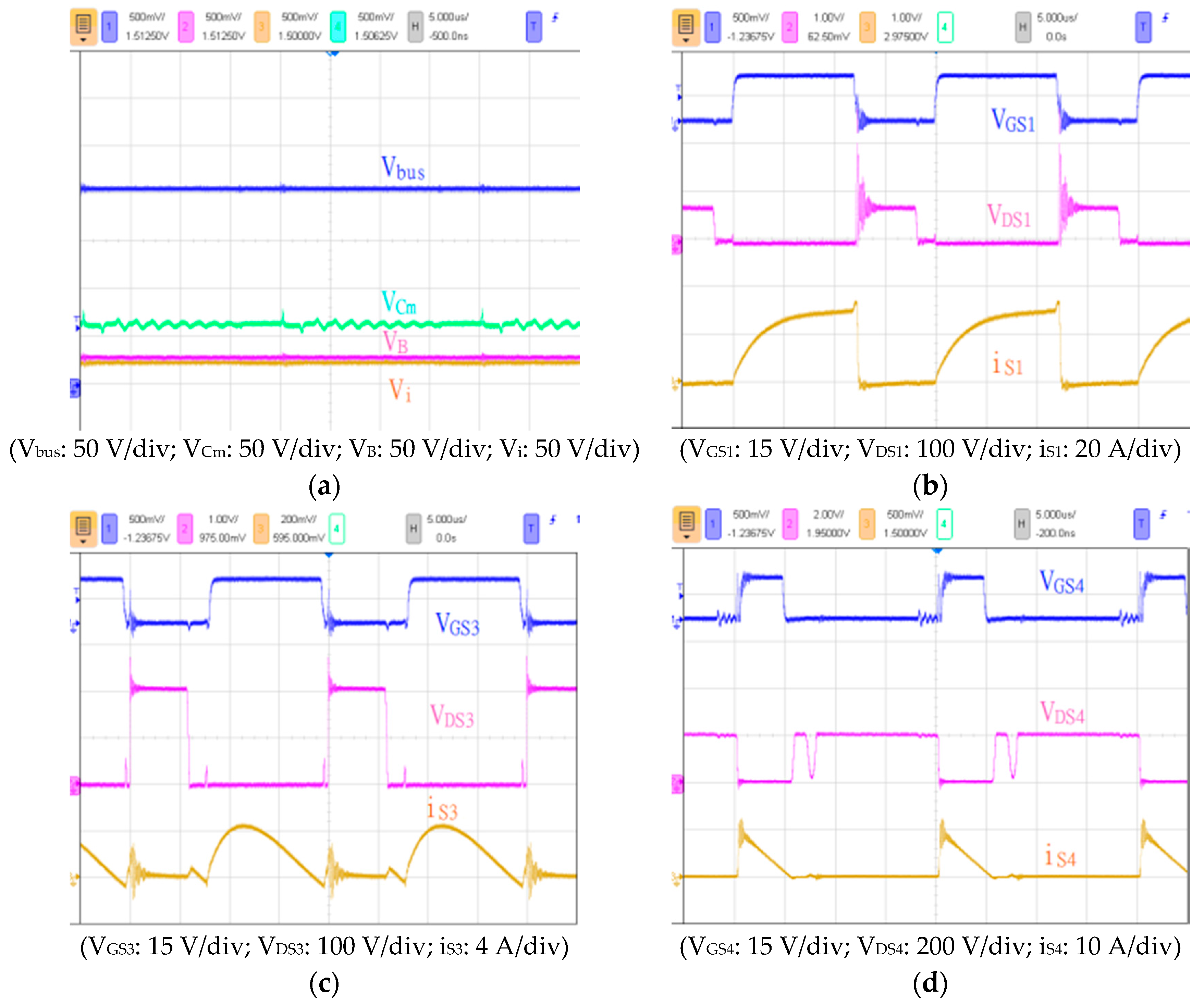
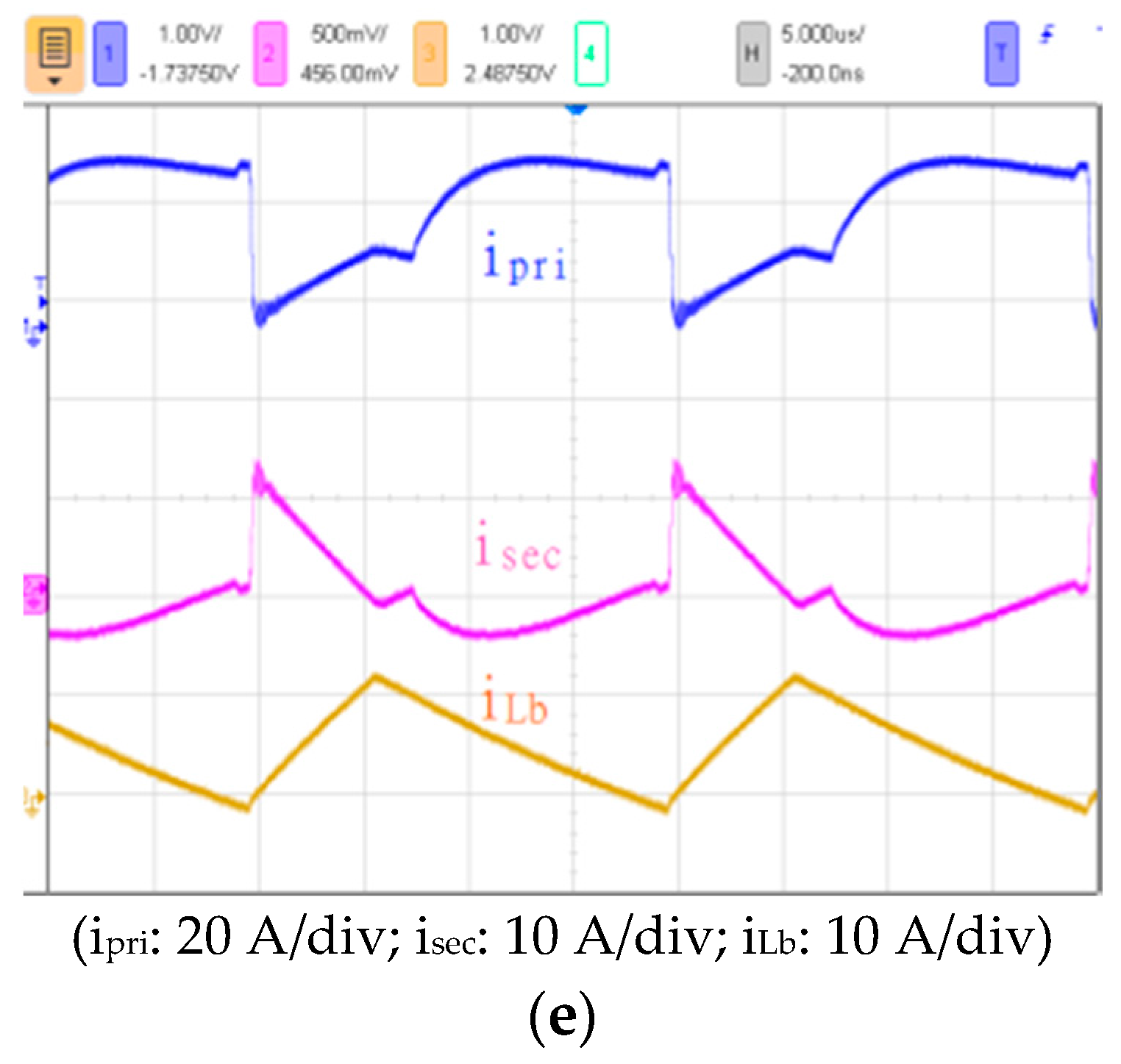
Figure 15 shows the measurement results for the proposed converter for Stage 1. Figure 15a shows the voltage waveforms of the DC bus Vbus, voltage-doubling capacitor VCm, battery VB, and input Vi. Figure 15b–d show the waveforms of the drive signal Vgs, switch voltage Vds, and switch current is of switches S1, S3, and S4 for the full load, and Figure 15e depicts the current waveforms of the transformer (ipri and isec) and inductor (iLb) for the same load. Figure 15 shows that the voltage stresses of S1, S3, and S4 are approximately 90, 150, and 90 V, respectively. The surge resulting from the leakage inductance when a switching is turmed off is suppressed, and Vbus is 200 V.
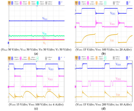

Figure 15.
Measurement results for Stage 1 for a load of 500 W: (a) output voltage waveforms; (b) switch S1 waveforms; (c) switch S3 waveforms; (d) switch S4 waveforms; and (e) current waveforms of the transformer and inductors.
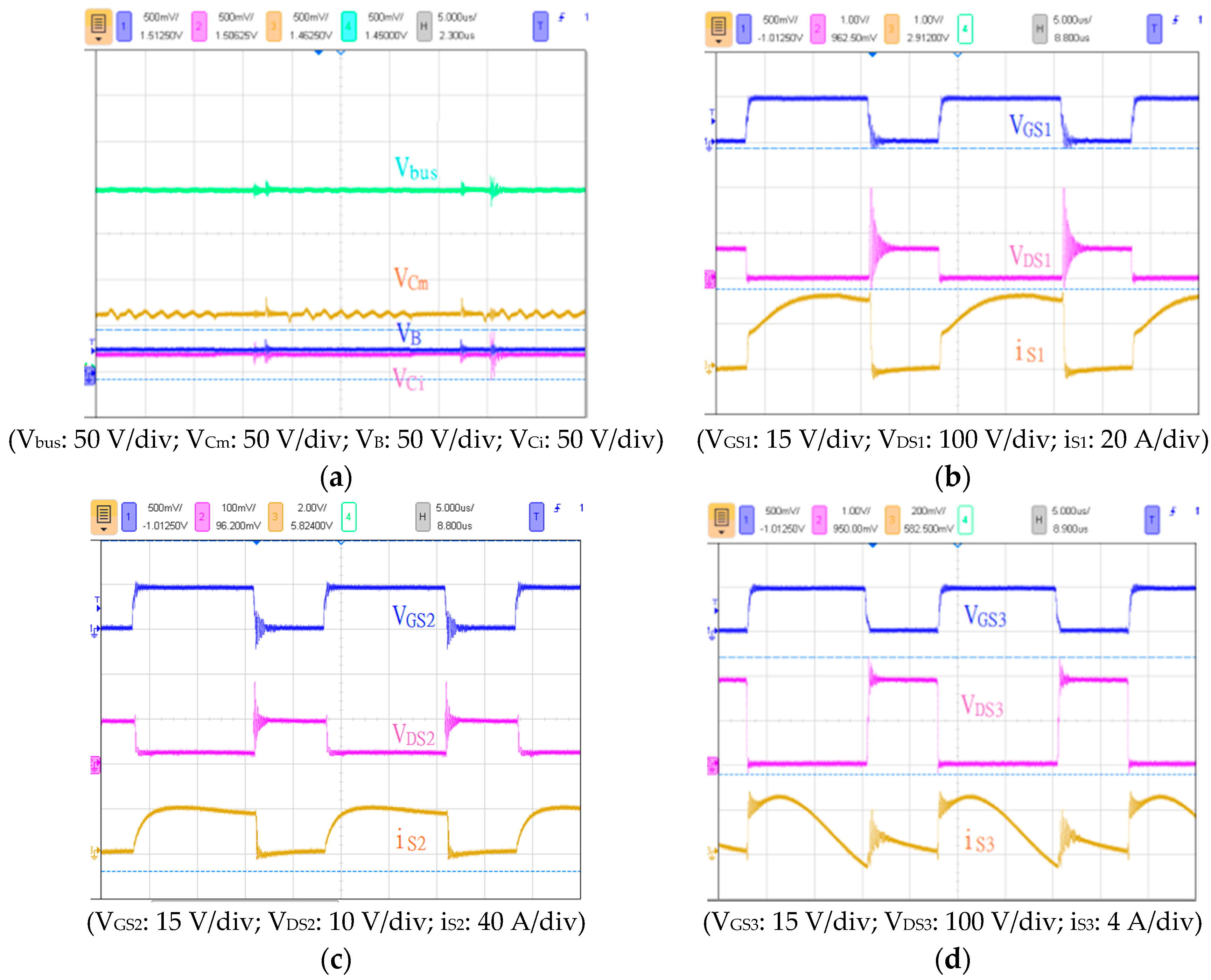
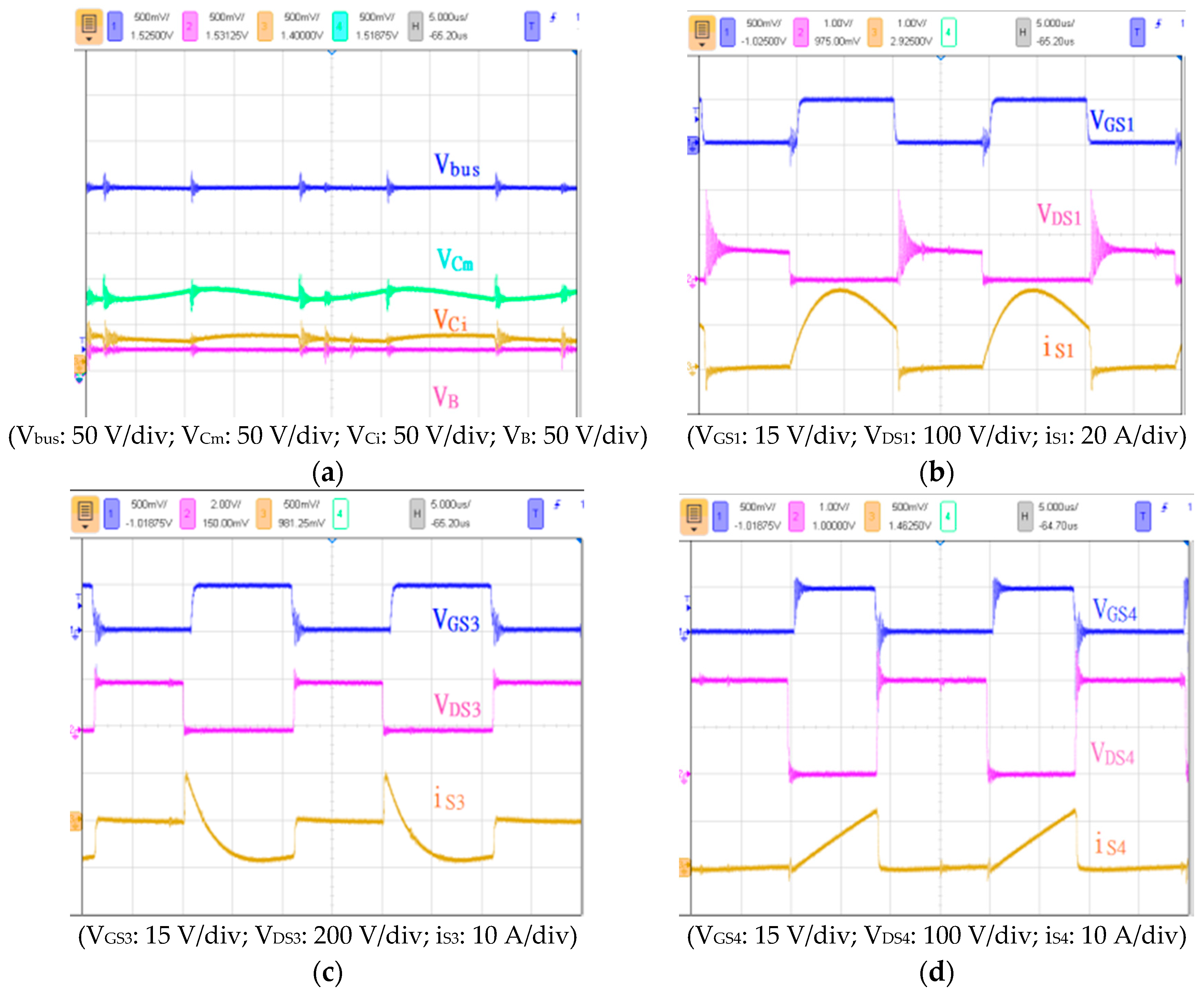
Figure 16 shows the measurement results for the proposed converter for Stage 2. Figure 16a shows the waveforms of Vbus, VCm, VB, and Vi. Figure 16b–e show the waveforms of Vgs, Vds, and is for switches S1, S2, S3, and S4 for the full load. Furthermore, Figure 16f presents the waveforms of ipri, isec, and iLb for the full load. Figure 16 shows that Vbus is 200 V and that the voltage stresses of S1, S2, S3, and S4 are approximately 90, 90, 160, and 160 V, respectively.

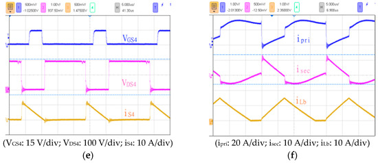
Figure 16.
Measurement results for Stage 2: (a) output voltage waveforms; (b) switch S1 waveforms; (c) switch S2 waveforms; (d) switch S3 waveforms; (e) switch S4 waveforms; and (f) current waveforms of the transformer and inductors.
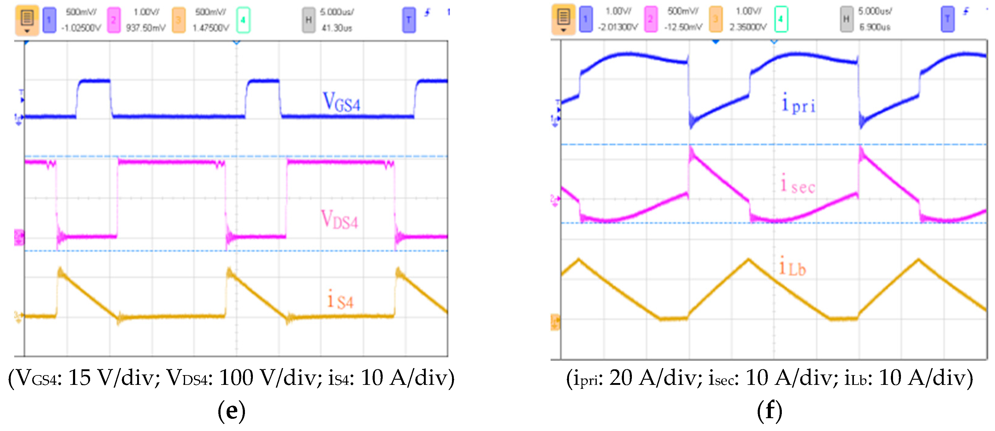
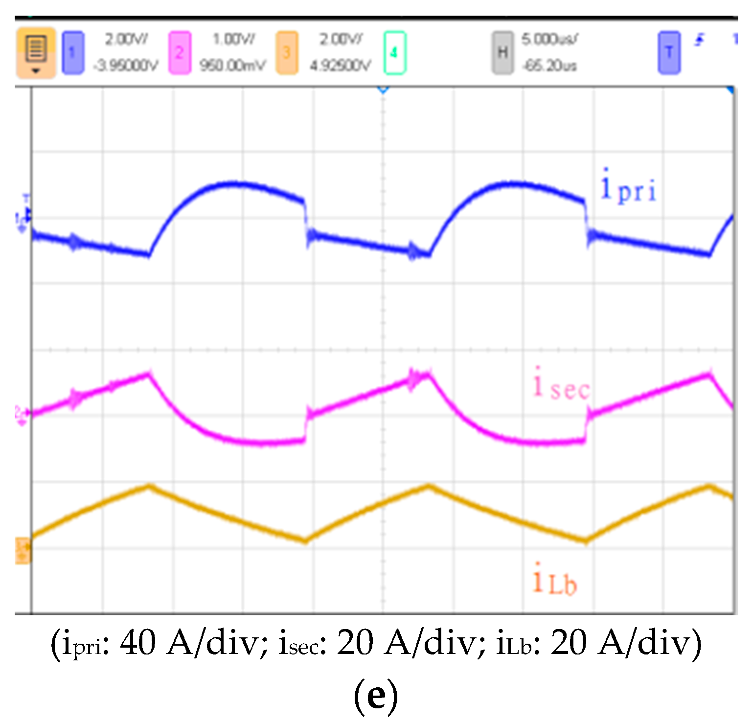
Figure 17 shows the measurement results for the proposed converter for Stage 3. Figure 17a presents the waveforms of Vbus, VCm, VB, and Vi. Furthermore, Figure 17b–d shows the waveforms of Vgs, Vds, and is for switches S1, S3, and S4 for the full load, and Figure 17e depicts the waveforms of ipri, isec, and iLb for the same load.
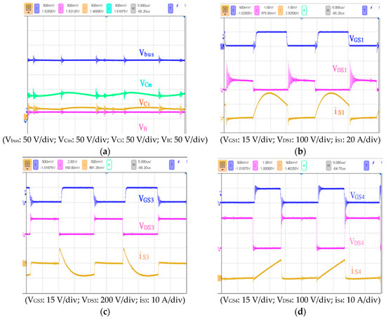
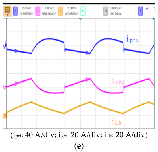
Figure 17.
Measurement results for Stage 3: (a) output voltage waveforms; (b) switch S1 waveforms, (c) switch S3 waveforms; (d) switch S4 waveforms; and (e) current waveforms of the transformer and inductors.
5. Conclusions
This paper presents a theoretical analysis of the steady state, related considerations, and experimental results of the proposed three-port bidirectional DC/DC converter. The converter operates in a PV step-up mode, battery step-up mode, and DC bus step-down mode, reflecting the high circuit functionality of the circuit. An improved boost-flyback converter and a DC -blocking capacitor are included on the low-voltage side and high-voltage side, respectively, to increase the voltage conversion ratio and to reduce the voltage on the transformer, both of which are necessary for high step-down performance. In addition, the energy stored in the leakage inductor is recycled, which improves the overall efficiency of the system. The proposed converter offers the advantages of high efficiency, a high step-up/step-down ratio (8–10/8.33), small system size, and low cost. Finally, a 500 W three-port bidirectional converter was implemented to verify its feasibility and practicability. The highest efficiencies of the proposed converter for operation in the PV step-up stage, battery step-up stage, and step-down stage were 95.2%, 94.2%, and 97.6%, respectively, and the highest efficiencies associated with the maximum output power were 91%, 94%, and 96%, respectively.
Author Contributions
These authors contributed equally to this work.
Conflicts of Interest
The authors declare no conflict of interest.
Nomenclature
| Lm | Magnetization inductor |
| Co | Output Capacitor |
| N1 | Primary Turns |
| LLk1 | Primary Leakage |
| Vo | Output Voltage |
| V2 | Second Voltage |
| VLk1 | Primary Leakage Voltage |
| Ts | Switch period |
| GVo | Step-up voltage conversion ratio |
| io | Output Current |
| iLb | Charge Current |
| iS1 | Switch S1 Current |
| iS4 | Switch S4 Current |
| VS2 | Switch S2 Voltage Stress |
| VD1 | Diode D1 Voltage Stress |
| Lb | Charger inductor |
| Cm | Double Voltage Capacitor |
| N2 | Second Turns |
| LLk2 | Second Leakage |
| Vb | Battery Voltage |
| VCi | Input Capacitor Voltage |
| VLk2 | Second Leakage Voltage |
| Ton | Switch turn-on time |
| GVb | Step-down voltage conversion ratio |
| iLm | Magnetization inductor Current |
| ipri | Primary Current |
| iS2 | Switch S2 Current |
| iLb(max) | Charger Maximum Current |
| VS3 | Switch S3 Voltage Stress |
| VD2 | Diode D2 Voltage Stress |
| Ci | Input Capacitor |
| Do | PV Blocking Diode |
| N | Turns ratio |
| Vi | PV input Voltage |
| V1 | Primary Voltage |
| VCm | Double Voltage Capacitor Voltage |
| D | Switch Duty Cycle |
| Toff | Switch turn-off time |
| iin | PV Input Current |
| ib | Battery Charge Current |
| isec | Second Current |
| iS3 | Switch S3 Current |
| VS1 | Switch S1 Voltage Stress |
| VS4 | Switch S4 Voltage Stress |
References
- Response to the Framework Convention on Climate Change News in Taiwan. Available online: http://www.tri.org.tw/unfccc/ (accessed on 12 March 2015). (In Chinese).
- Ministry of Economic Affairs Bureau of Energy 2014 Energy and Industrial Technology White Paper. Available online: http://www.moeaboe.gov.tw/ECW/populace/content/SubMenu.aspx?menu_id=3282 (accessed on 12 March 2015).
- Ismail, E.H.; Al-Saffar, M.A.; Sabzali, A.J. High Conversion Ratio DC-DC Converters with Reduced Switch Stress. IEEE Trans. Circ. Syst. I 2008, 55, 2139–2151. [Google Scholar] [CrossRef]
- Li, W.; Lv, X.; Li, W.; Lv, X.; Deng, Y.; Liu, J.; He, X. A Review of Non-Isolated High Step-Up DC/DC Converter in Renewable Energy Applications. In Proceedings of the Twenty-Fourth Annual IEEE Applied Power Electronics Conference and Exposition (APEC 2009), Washington, DC, USA, 15–19 February 2009; pp. 364–369. [Google Scholar]
- Zhao, Q.; Lee, F.C. High Performance Coupled-Inductor DC-DC Converters. In Proceedings of the Eighteenth Annual IEEE Applied Power Electronics Conference and Exposition (APEC ‘03), Miami, FL, USA, 9–13 February 2003; Volume 1, pp. 109–113. [Google Scholar]
- Huber, L.; Jovanovic, M.M. A design approach for server power supplies for networking applications. In Proceedings of the Fifteenth Annual IEEE Applied Power Electronics Conference and Exposition (APEC 2000), Los Angeles, CA, USA, 21–25 February 2000; pp. 1163–1169. [Google Scholar]
- Feng, X.G.; Liu, J.J.; Lee, F.C. Impedance specifications for stable DC distributed power systems. IEEE Trans. Power Electron. 2002, 17, 157–162. [Google Scholar] [CrossRef]
- Wu, T.F.; Yu, T.H. Unified approach to developing single-stage power converters. IEEE Trans. Aerosp. Electron. Syst. 1998, 34, 211–223. [Google Scholar]
- Luo, F.L.; Ye, H. Positive output super-Lift converters. IEEE Trans. Power Electron. 2003, 18, 105–113. [Google Scholar]
- Zhao, Q.; Tao, F.; Lee, F.C. A Front-end DC/DC Converter for Network Server Applications. In Proceedings of the 2001 IEEE 32nd Annual Power Electronics Specialists Conference (PESC), Vancouver, BC, Canada, 17–21 June 2001; Volume 3, pp. 1535–1539. [Google Scholar]
- Wai, R.J.; Duan, R.Y. High step-up converter with coupled-inductor. IEEE Trans. Power Electron. 2005, 20, 1025–1035. [Google Scholar] [CrossRef]
- Chen, F.; Amirahmadi, A.; Batarseh, I. Zero voltage switching Forward-Flyback Converter with efficient active LC snubber circuit. In Proceedings of the 2014 IEEE Applied Power Electronics Conference and Exposition (APEC), Fort Worth, TX, USA, 16–20 March 2014; pp. 2041–2047. [Google Scholar]
- Jianhua, W.; Fanghua, Z.; Chunying, G.; Ran, C. Modeling and analysis of a buck/boost bidirectional converter with developed PWM switch model. In Proceedings of the 8th International Conference on Power Electronics (ECCE Asia), Shilla Jeju, Korea, 30 May–3 June 2011. [Google Scholar]
- Mohammadi, M.R.; Farzanehfard, H. A new bidirectional ZVS-PWM Cuk converter with active clamp. In Proceedings of the 2011 19th Iranian Conference on Electrical Engineering, Tehran, Iran, 17–19 May 2011; pp. 1–6. [Google Scholar]
- Dimna Denny, C.; Shahin, M. Analysis of bidirectional SEPIC/Zeta converter with coupled inductor. In Proceedings of the 2015 International Conference on Advancements in Power and Energy (TAP Energy), Kollam, India, 24–26 June 2015; pp. 103–108. [Google Scholar]
- Song, Y.; Enjeti, P.N. A new soft switching technique for bi-directional power flow, full-bridge DC-DC converter. In Proceedings of the 2002 37th IAS Annual Meeting Industry Applications Conference, Harrisburg, PA, USA, 13–18 October 2002; Volume 4, pp. 2314–2319. [Google Scholar]
- Ma, Z.; Hu, R. Zero-voltage-switching Condition of isolated-type Symmetrical Half-bridge Bidirectional DC/DC Converter. In Proceedings of the Electrical and Control Engineering (ICECE), Yichang, China, 16–18 September 2011; pp. 2347–2350. [Google Scholar]
- Chen, Y.-T.; Wei, S.-Y. A multiple-winding bidirectional flyback converter used in the solar system. In Proceedings of the Next-Generation Electronics (ISNE), Kaohsiung, Taiwan, 25–26 February 2013; pp. 130–133. [Google Scholar]
- Saranya, P.S.; Lekshmi, R. Chandran Analysis of bidirectional flyback converter. In Proceedings of the Computation of Power, Energy Information and Communication (ICCPEIC), Chennai, India, 22–23 April 2015; pp. 425–429. [Google Scholar]
- Wu, H.; Sun, K.; Chen, L.; Zhu, L.; Xing, Y. High Step-Up/Step-Down Soft-Switching Bidirectional DC–DC Converter With Coupled-Inductor and Voltage Matching Control for Energy Storage Systems. IEEE Trans. Ind. Electron. 2016, 63, 2892–2903. [Google Scholar] [CrossRef]
- Liang, T.-J.; Lee, J.-H. Novel High-Conversion-Ratio High-Efficiency Isolated Bidirectional DC–DC Converter. IEEE Trans. Ind. Electron. 2015, 62, 4492–4503. [Google Scholar] [CrossRef]
- Wai, R.-J.; Liaw, J.-J. High-Efficiency-Isolated Single-Input Multiple-Output Bidirectional Converter. IEEE Trans. Ind. Electron. 2015, 30, 4914–4930. [Google Scholar] [CrossRef]
- Nathan, M.S.; Rajasekaran, R.; Rani, P.U. Rules based functional control of bidirectional DC-DC converter for stand-alone PV with hybrid energy storage system. In Proceedings of the Innovations in Information, Embedded and Communication Systems (ICIIECS), Coimbatore, India, 19–20 March 2015; pp. 1–6. [Google Scholar]
- Krishnaswami, H.; Mohan, N. Three-port series-resonant DC-DC converter to interface renewable energy sources with bidirectional load and energy storage ports. IEEE Trans. Power Electron. 2009, 24, 2289–2297. [Google Scholar] [CrossRef]
- Wang, Z.; Li, H. An integrated three-port bidirectional DC-DC converter for PV application on a DC distribution system. IEEE Trans. Power Electron. 2013, 28, 4612–4624. [Google Scholar] [CrossRef]
- Wu, H.; Sun, K.; Chen, R.; Hu, H.; Xing, Y. Full-bridge three-port converters with wide input voltage range for renewable power systems. IEEE Trans. Power Electron. 2012, 27, 3965–3974. [Google Scholar] [CrossRef]
- Zeng, J.; Qiao, W.; Qu, L. An Isolated Three-Port Bidirectional DC-DC Converter for Photovoltaic Systems with Energy Storage. IEEE Trans. Ind. Appl. 2015, 51, 3493–3503. [Google Scholar] [CrossRef]
- Li, W.; Xu, C.; Luo, H.; Hu, Y.; He, X.; Xia, C. Decoupling-Controlled Triport Composited DC/DC Converter for Multiple Energy Interface. IEEE Trans. Ind. Electron. 2015, 62, 4504–4513. [Google Scholar] [CrossRef]
- Hu, Y.; Xiao, W.; Cao, W.; Ji, B.; Morrow, D.J. Three-Port DC–DC Converter for Stand-Alone Photovoltaic Systems. IEEE Trans. Ind. Electron. 2015, 30, 3068–3076. [Google Scholar] [CrossRef]
- Tao, H.; Kotsopoulos, A.; Duarte, J.L.; Hendrix, M.A.M. Family of multiport bidirectional DC-DC converters. IEE Proc. Electr. Power Appl. 2006, 153, 451–458. [Google Scholar] [CrossRef]
- Li, W.; Xiao, J.; Zhao, Y.; He, X. PWM plus phase angle shift (PPAS) control scheme for combined multiport DC/DC converters. IEEE Trans. Power Electron. 2012, 27, 1479–1489. [Google Scholar] [CrossRef]
- Kim, S.Y.; Song, H.-S.; Nam, K. Idling port isolation control of three-port bidirectional converter for Evs. IEEE Trans. Power Electron. 2012, 27, 2495–2506. [Google Scholar] [CrossRef]
- Phattanasak, M.; Gavagsaz-Ghoachani, R.; Martin, J.-P.; Nahid-Mobarakeh, B.; Pierfederici, S.; Davat, B. Control of a hybrid energy source comprising a fuel cell and two storage devices using isolated three-port bidirectional DC-DC converters. IEEE Trans. Ind. Appl. 2015, 51, 491–497. [Google Scholar] [CrossRef]
- Chien, L.-J.; Chen, C.-C.; Chen, J.-F.; Hsieh, Y.-P. Novel three-port converter with high-voltage gain. IEEE Trans. Power Electron. 2014, 29, 4693–4703. [Google Scholar] [CrossRef]


© 2017 by the authors. Licensee MDPI, Basel, Switzerland. This article is an open access article distributed under the terms and conditions of the Creative Commons Attribution (CC BY) license (http://creativecommons.org/licenses/by/4.0/).