Abstract
To overcome the problem of switching loss during the balancing process, a novel cell balancing circuit is proposed with the integration of a zero current switching technique. Moreover, the balancing circuit proposed can change between a classical buck-boost pattern and a resonant switched-capacitor pattern with flexible control to cater to the balancing requirements under different driving scenarios. The results of the simulation of field experiments demonstrate successful balancing, various balancing speed, and low energy loss. The proposed balancing circuit proves to be effective for a wide range of application and is the first attempt to integrate a dual balancing function in a single balancing circuit for cells.
1. Introduction
The pursuit of better battery performance has become the top challenge for electric vehicle (EV) design, as it primarily determines the driving mileage and manufacturing cost [1,2,3,4]. With the fast development of a supercapacitor (SC), the battery and SC strings composed of a large number of series and parallel-connected cells are usually used to formulate a hybrid energy package for better power performance [5,6,7,8]. Moreover, increasing numbers of researchers are collecting retired batteries for second-life application, hoping to cut costs while maintaining a qualified driving performance. Due to non-uniform individual cell properties, a certain imbalance may be easily generated among voltages of different cells during charging and discharging processes. As the effect of imbalance is accumulative and leads to battery deterioration, voltage balancing is necessary to guarantee the safe operation of the hybrid energy package [9,10,11].
Researchers have done many state-of-the-art works on promoting the balancing efficiency and balancing speed and decreasing loss. The passive balancing method is the most commonly adopted technique. Resistors in parallel with the cell strings are switched on when the cells get close to the peak withstanding voltage or when they have a higher state-of-charge (SoC) than other cells. This method generates additional heating loss because the energy dissipates into resistors during balancing process [12]. For energy-saving purposes, an active balancing method is put forward so that the charging and discharging current of each cell can be controlled to keep the same SoC among all cell units for the higher energy to be transferred into the cells with lower energy using a power converter circuit, instead of wasting it as heat loss. This method has proven to be more efficient, hence, many advanced voltage equalizers have been designed based on the active method using converters [13,14], switched-capacitors [15,16,17,18], transformers [7] or switched inductors [19,20]. However, those methods are not flexible enough for changing scenarios. Furthermore, as a hard switching operation is adopted in a large number of cell balancing circuits [21,22,23], electromagnetic interference (EMI) and high switching energy loss will appear. On the other hand, the service life of energy sources will also be affected by a current spike in hard switching circuits. In this paper, a novel balancing circuit is proposed to realize zero-current switching (ZCS) similar to quasi-resonant [24,25] during the switched-capacitor mode and has been proven to further reduce energy loss [24,25,26,27,28,29].
Different states of EVs, such as the drive state, brake state, and park state, may have different requirements on the output power, balancing speed, and balancing loss. Many existing papers [22,23] do not take the real driving state into account and make a fixed cell balancing strategy, which decreases the overall balancing efficiency [30,31,32,33]. They are based on switched-capacitor techniques [34,35]. Some papers have realized the difference in energy management at different driving states and proposed specific energy controllers respectively. The energy saving controller for electric mining trucks is introduced in Reference [36], as it runs in high-frequency start-up processes. A predictive energy controller based on preceding vehicle movement management is designed in Reference [37] for lined up EVs on the road. A real-time energy controller for EVs in a charge-depletion mode is discussed in References [38,39,40] for adaptive energy consumption minimization.
In this paper, a novel and multi-functional balancing circuit is proposed with a ZCS technique to improve energy saving during the balancing process. The multi-functional circuit can easily change between a buck-boost pattern and switched-capacitor pattern with flexible switching frequency and duty ratios, i.e., the circuit can adapt to changing driving states. Figure 1 demonstrates six different operating modes with different cell balancing requirements for the corresponding driving states. Moreover, voltage sensors can be installed at each cell in order to collect the voltage signals for an intelligent control box. In the real-time feedback control, switching frequency and duty ratios are adjusted to accelerate voltage balancing process and decrease loss. This paper is the first attempt to use the ZCS technique in the integrated balancing circuit for rapid mode switching, accurate voltage tracking, and loss reduction. The circuit configuration, operation principle, and equations are presented in Section 2 and Section 3. The results of the simulation and field experiment are presented in Section 4 and Section 5. Section 6 concludes this paper.
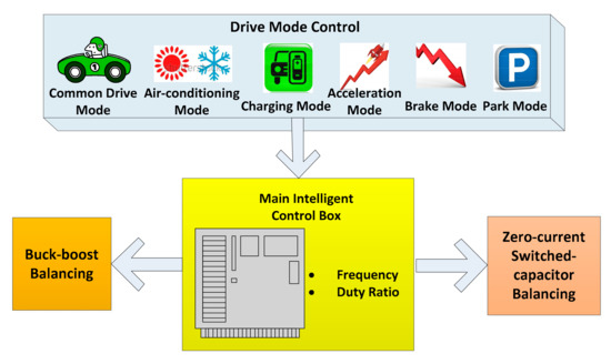
Figure 1.
Different operating modes and requirements.
2. Proposed Cell Balancing Circuits
2.1. Circuit Configuration
In this section, a series multi-functional balancing circuit is presented for analysis. Different states of EVs, such as the drive state, brake state, and park state, may have different requirements on the output power, balancing speed, and balancing loss. Figure 1 demonstrates six different operating modes with different cell balancing requirements for the corresponding driving states. For example, EVs in acceleration desire a high balancing speed and low loss while the park state does not have requirements on the balancing speed. The circuitry of Figure 2 shows the SC cells (SC1, SC2, …, SCn) in series connection. In the n-cells voltage balancing system, there are n − 1 switched-capacitors and 4n − 4 switches which are dominated by the main intelligent control box to operate the circuit in different modes. All the switches are named in two groups Sa and Sb, the switches in each group are divided as Sa2m−1, Sa2m, Sa2m+1 and Sa2m+2, where m varies from 1 to n − 1; In Sb2m−1, Sb2m, Sb2m+1 and Sb2m+2, m varies from 1 to n − 1. This multi-functional balancing circuit has two operation states, buck-boost balancing and switched-capacitor balancing, under different control of inductors (L1, L2, …, Ln−1) and switched-capacitors (C1, C2, …, Cn−1). And the charge is transferred from a higher voltage SC to lower ones automatically. The proposed circuit changes its topology and parameters to cater to the operation requirements of different operation modes, such as the common drive mode, drive with air-conditioning mode, acceleration mode, brake mode, and park mode for EVs.
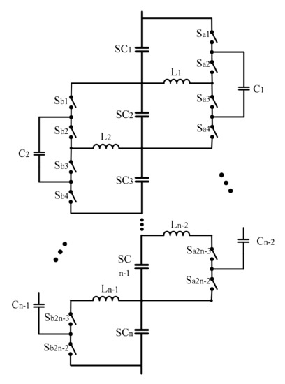
Figure 2.
Proposed balancing circuit.
2.2. Balancing Circuit Operation Analysis
In an ideal case, the switching frequency fs should be equal to the resonant frequency fr.
where ; R is the equivalent resistance, L is the inductance of the inductor and C is the capacitance of the switched-capacitor.
However, it is arduous to precisely match the RLC parameters of different balancing branches in real implementation. To avoid a reverse current of the resonant inductor, the switching frequency in the proposed switched-capacitor circuit should be slightly higher than the resonant frequency with regards to the tolerances of the RLC parameters.
There are two clock phase φa and φb in one switching period T, as shown in Figure 3. During the φa, the switches Sa2m−1, Sb2m−1 and Sa2m+1, Sb2m+1 are turned on, the circuit forms the switched-capacitors resonant tanks series connecting with switched-capacitors as shown in Figure 4a,b. Meanwhile, Figure 4c,d are in a buck-boost mode state during the φb, when Sa2m−1, Sb2m−1 and Sa2m, Sb2m are turned on, there is only an inductor connect with SC. These two functioning modes operate alternatively with a high frequency control signal. They are divided into ZCS mode state I, ZCS mode state II, buck-boost mode state I and buck-boost mode state II which will be discussed in Section 2.3.
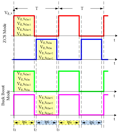
Figure 3.
Control signal of the switches.
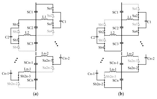
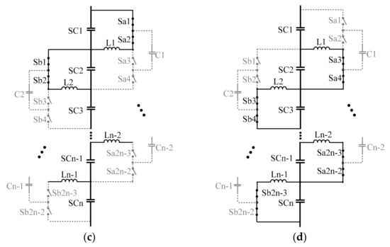
Figure 4.
Working principle of the proposed balancing system. (a) ZCS mode state I; (b) ZCS mode state II; (c) buck-boost mode state I; (d) buck-boost mode state II.
2.3. Analysis of ZCS Operation
When the switches Sa2m−1, Sb2m−1 and Sa2m+1, and Sb2m+1 are turned on, the circuit forms the switched-capacitors resonant tanks as shown in Figure 5. In the state of the ZCS-SC, charge will transfer from SCk to Ck switched-capacitor tank when the voltage of SCk is higher than the initial voltage of Ck. Therefore, Ck is charged and the control signal during the process is shown in the top curve of Figure 5 and Table 1. In a similar way, the charge will transfer from Cj to SCj when the voltage of SCj is lower than the initial voltage of Cj. Cj is discharged in this process and the control signal is shown in the bottom curve of Figure 5 and Table 1. SCk, Ck, Lk and SCj, Cj, Lj form the resonant loops. The rSC, rC, rS, and rL internal resistors for SCs, switched-capacitors, ON-resistance of the switches, and inductors, respectively. In order to simplify the operation analysis, the internal resistance will first be ignored. All the components are ideal.
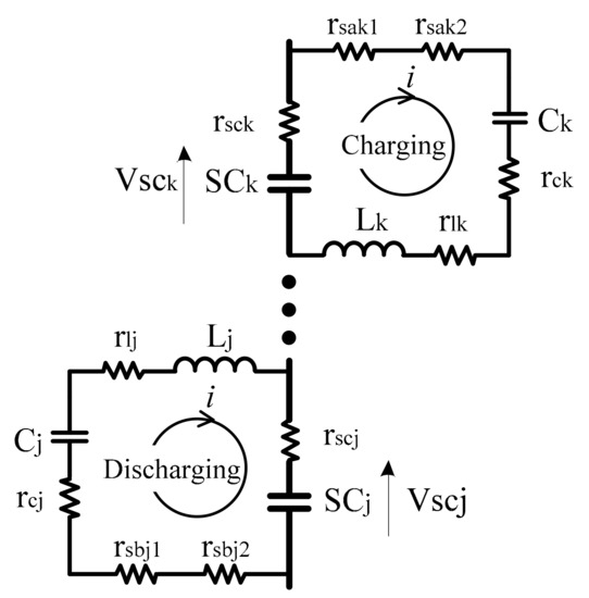
Figure 5.
Circuit of ZCS mode.

Table 1.
Switches control logical signal.
(1) State I (See Figure 5 charging circle)
In the state when Sa2m−1 and Sa2m+1 are turned on and Sa2m and Sa2m+2 are turned off. Assume that all the components here are ideal and there is zero internal resistance for the SCs, switched-capacitors, inductors, and switches in this analysis. The relationship between the current and the voltage are as shown below:
where Lk is the inductance of inductor Lk; VSCk is the voltage of SCk.
Then, the variations of the VCk and ir of the above are
where ΔVCk is the peak-to-peak amplitude of VCk; Ir is the amplitude of the ir; ω is the resonant angular frequency which is , Ck is the capacitance of Ck.
In this resonant period, assume that the initial voltage VCmin across the capacitor Ck is minimum voltage, which is lower than the voltage VSCk across the SCk. The initial voltage VLk and the amplitude of the ir are:
After half a resonant period, the voltage of the VCk could reach maximum VCk_max, which is shown below:
(2) State II (See Figure 5 discharging circle)
In the state when Sb2m−1 and Sb2m+1 are turned on and Sb2m and Sb2m+2 are turned off, the switched-capacitor Cj is discharging SCj and the resonant current ir is increasing in the opposite direction. Similarly as state I, the amplitude of the resonant current is
The voltage of VCj could reach minimum VCj_min at the end of this resonant period.
In fact, there are equivalent series resistance (ESR) for the components and the voltage drop across the switches that cannot be ignored. The rSC, rC, rS, and rL internal resistors for SCs, switched-capacitors, ON-resistance of the switches and inductors respectively should be considered in the following analysis. The total ESR RESR in one resonant tank of the circuit is RESR = rSC+ rC+ rL+ 2rS.
The resonant current of charging and discharging state should be revised as:
State I:
State II:
where , .
Lk,j refers to either Lk or Lj in each of their state I and II and hence ρ and ωr are calculated according to their respective Lk or Lj in State I and State II. The maximum and minimum voltage of VCk,j are
3. Modeling for Balancing Mode
3.1. Modeling for ZCS Balancing Mode
As it is shown in Figure 6, SC cells can be formulated to be charged or discharged between each other with the equivalent resistance. In the resonant circuit, Ck, Lk and Cj, Lj has the same value C and L, respectively, and all the switches are the same. The voltage of VC could achieve the maximum VC_max at the end of the state I and be reduced to the minimum at the end of state II. The voltage ripple ΔVC can be obtained by subtracting (14) from (13).
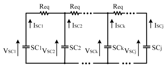
Figure 6.
Model of the ZCS mode circuit.
In one switching cycle the quantity of electric charge is CΔVC, flowing from higher voltage cell to lower voltage cell. The average current Iavg_r of one cycle is
When ΔVC in (15) is substituted into (16), the equivalent resistance Req of each resonant tank is
The power loss Ploss_r of the ZCS mode is shown below
3.2. Modeling for Buck-Boost Balancing Mode
During the progress of the buck-boost balancing mode, the charging/discharging varies in one cycle, the charge is transferred between SCk and SCj. The equivalent model of the balancing circuit is shown in Figure 7, where the ESR and the on-state voltage for the diode are included to facilitate modeling.
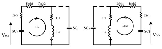
Figure 7.
Model of the buck-boost mode circuit under charging and discharge.
To illustrate the voltage conversion process for the inductor L1, the mmf values of M_ch and M_disch to investigate the voltage conversion of the converter circuit for charging and discharging, respectively, during one cycle are
where D1 and D2 are the turn-on duty ratio of switches for charging and discharging, respectively, D1 + D2 = 1.
Considering volt-second balancing of L1, the relationship between two cells is
where R1 = 2rS + rL + rSCk, R2 = 2rS + rL + rSCj; ich and idisch are instantaneous current across L1 for charging and discharging, respectively. Iavg_ch and Iavg_disch are the average current across L1 when it is charging or discharging.
When and , Iavg_ch could be obtained from (21) as:
The average current Iavg_b of SC in this mode is
In the balancing progress, all the energy transfers between each cell, from the higher voltage SC cell to lower voltage cell. During these states, the variation of the ich is
where Δich is the current difference during charging state, .
The variation of the idisch is
where Δidisch is the current difference during discharging state.
The energy discharged Edisch from SCk and the energy charged Ech to the SCj throughout one cycle are:
The energy transferred in the inductor L1 is
The energy loss Eloss could be obtained by subtracting Equation (27) from (26).
where .
The power loss Ploss_b of the buck-boost mode is
4. Simulation Results of the Multi-Function Voltage Equalizer
In PSIM software, the proposed circuit is simulated. The circuit topologies of three series connected SCs with initial voltages of 2.0, 2.4, 2.6 V, respectively, and with the same capacitance 1F are built in the simulation shown in Figure 8. Switched-capacitors C = 22 μF are used in simulation while fs = 15, 20, 25 kHz and 90, 100, 110 kHz of the control signals are used to operate the circuit. The above configurations are the same with practical application, except the capacitance of the SCs.
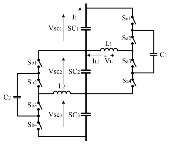
Figure 8.
Multi-functional equalizer built in laboratory.
Table 2 illustrates the comparison of the waveforms in the simulation varied with a different switching frequency fs for ZCS and buck-boost mode. It is observed that VSC1, VSC2, and VSC3 finally converge to the same voltage level in all circumstances. For the ZCS mode, when fs is larger, the switching speed is faster that accelerates the equalization process.
Table 2.
Simulation results of the switched-capacitor voltage equalizer.
Figure 9 shows the simulation results of the ZCS mode under 20 kHz frequency with 350 F SCs. At 32 s the balancing progress was about 10%, the voltage between VSC1 and VSC2 are 0.18 V at this moment. The balancing progress reached approximately 90% at 290 s when the difference reduces to 0.02 V. And the variations of the voltage of the switched-capacitor C1 and current I1 are shown in this figure.

Figure 9.
Simulation results of ZCS mode under 20 kHz frequency with 350 F SCs.
The balancing phenomenon conforms to the principles in Equation (16). When the switching frequency fs is the same as the resonant frequency fr the balancing progress could reach zero current when switches are turn on and off, this conforms to the principle in Equation (1). But the variation of the fs could not affect the balancing speed for buck-boost mode which is illustrated in Equation (23).
5. Experimental Results of the Multi-Function Circuit
The proposed circuit has advantages in performing balancing for different EV driving modes so that it is more flexible for an energy storage system which has different working conditions. To verify the mathematical derivation and software simulation, energy storage strings composed of three SCs were formulated with the multi-functional balancing circuit controlled by different switching signals. The topology is shown in Figure 8 and the list of components is recorded in Table 3. Figure 10 is the supercapacitor test platform used in the laboratory.
Table 3.
Parameters in the experiment.
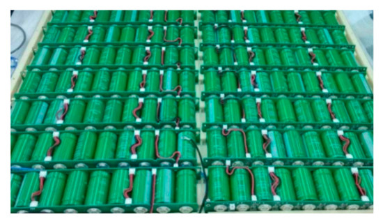
Figure 10.
The supercapacitor test platform.
The voltage balancing process for the ZCS mode of the experiment is shown in Figure 11. The initial voltages of the SCs are 2.6 V, 2.31 V, and 1.88 V, respectively. After the voltage balancing was conducted, VSC1 VSC2 and VSC3 were all finally balanced to the same voltage magnitude, which coincides with the results in the above theoretical analysis. The integrated voltage magnitude after balancing was 2.23 V. Figure 12 depicts the voltage and current variations of C1, C2, and L1. It is clearly shown that when the switch turns on/off, the instantaneous current of the resonant loop is close to zero, which conforms to the principles of ZCS and loss reduction.
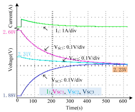
Figure 11.
The ZCS mode balancing waveform from the experiment in the laboratory.
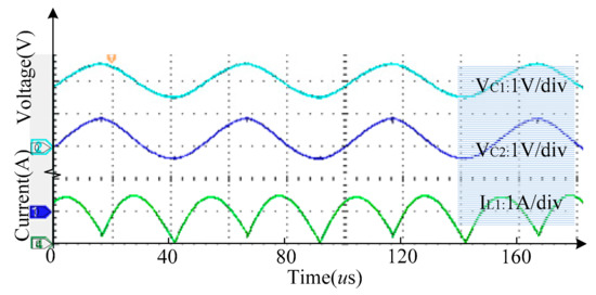
Figure 12.
The voltage VC1,2 and current IL1 waveform of switched-capacitor C1 during the balancing progress of ZCS mode.
The voltage balancing process for the buck-boost mode of the experiment is shown in Figure 13. The initial voltages of the SCs were set as 2.42 V, 2.29 V and 2.03 V, respectively. After conducting voltage balancing, VSC1 VSC2 and VSC3 were also balanced to the same voltage magnitude, as expected. The integrated voltage magnitude after balancing operation was 2.17 V. Figure 14 depicts the voltage and current variations of L1. The energy loss of ZCS mode decreased 35% compared with that in buck-boost mode.
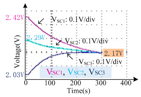
Figure 13.
The buck-boost mode balancing waveform from the experiment in the laboratory.
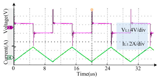
Figure 14.
The voltage VL1 and current IL1 waveform of switched-capacitor C1 during the balancing progress of buck-boost mode.
The experimental results demonstrate that the variations of both voltage and current in the proposed circuit conform to the charging/discharging principles analyzed in each phase.
6. Conclusions
A novel zero-current switching cell balancing circuit is proposed in this paper to decrease switching loss during balancing process. Furthermore, in order to adjust to different requirements of EV operation states, the multi-functional circuit was able to easily change between buck-boost and switched-capacitor pattern with flexible switching frequency and duty ratios. Simulation and field experiment were conducted to demonstrate its loss reduction effect and flexibility in various situations. The energy loss of the ZCS mode decreased 35% compared with that in the buck-boost mode. Future works may include voltage feedback control during the balancing process to further increase speed and decrease loss.
Author Contributions
X.W. proposed the theoretical models and conducted the experiment, K.W.E.C. gave the supervision and the ideas of the research work and Y.C.F. provided guidance and key suggestions.
Funding
This research was funded by Research Office, The Hong Kong Polytechnic University, Grant number G-YBLH.
Acknowledgments
The author gratefully thanks the support of Green Power Research Study 845G of The Hong Kong Polytechnic University.
Conflicts of Interest
The authors declare no conflict of interest.
References
- Fotouhi, A.; Auger, D.J.; Propp, K.; Longo, S. Electric vehicle battery parameter identification and SOC observability analysis: NiMH and Li-S case studies. IET Power Electron. 2017, 10, 1289–1297. [Google Scholar] [CrossRef]
- Kandasamy, K.; Vilathgamuwa, D.M.; Madawala, U.K.; Tseng, K.-J. Inductively coupled modular battery system for electric vehicles. IET Power Electron. 2016, 9, 600–609. [Google Scholar] [CrossRef]
- Ju, F.; Deng, W.; Li, J. Performance Evaluation of Modularized Global Equalization System for Lithium-Ion Battery Packs. IEEE Trans. Automat. Sci. Eng. 2016, 13, 986–996. [Google Scholar] [CrossRef]
- Brando, G.; Dannier, A.; Spina, I.; Tricoli, P. Integrated BMS-MMC Balancing Technique Highlighted by a Novel Space-Vector Based Approach for BEVs Application. Energies 2017, 10, 1628. [Google Scholar] [CrossRef]
- Guo, X.; Kang, L.; Huang, Z.; Yao, Y.; Yang, H. Research on a Novel Power Inductor-Based Bidirectional Lossless Equalization Circuit for Series-Connected Battery Packs. Energies 2015, 8, 5555–5576. [Google Scholar] [CrossRef]
- Ye, Y.; Cheng, K.W.E. An Automatic Switched-Capacitor Cell Balancing Circuit for Series-Connected Battery Strings. Energies 2016, 9, 138. [Google Scholar] [CrossRef]
- Xu, A.; Xie, S.; Liu, X. Dynamic voltage equalization for series connected ultracapacitors in EV/HEV applications. IEEE Trans. Veh. Technol. 2009, 58, 3981–3987. [Google Scholar]
- Choudhury, A.; Pillay, P.; Williamson, S.S. Comparative Analysis Between Two-Level and Three-Level DC/AC Electric Vehicle Traction Inverters Using a Novel DC-Link Voltage Balancing Algorithm. IEEE J. Emerg. Sel. Top. Power Electron. 2014, 2, 529–540. [Google Scholar] [CrossRef]
- Shili, S.; Hijazi, A.; Sari, A.; Lin-Shi, X.; Venet, P. Balancing circuit new control for supercapacitor storage system lifetime maximization. IEEE Trans. Power Electron. 2017, 32, 4939–4948. [Google Scholar] [CrossRef]
- Chemali, E.; Preindl, M.; Malysz, P.; Emadi, A. Electrochemical and Electrostatic Energy Storage and Management Systems for Electric Drive Vehicles: State-of-the-Art Review and Future Trends. IEEE J. Emerg. Sel. Top. Power Electron. 2016, 4, 1117–1134. [Google Scholar] [CrossRef]
- Cheng, K.W.E.; Divakar, B.P.; Wu, H.; Ding, K.; Ho, H.F. Battery-Management System (BMS) and SOC Development for Electrical Vehicles. IEEE Trans. Veh. Technol. 2011, 60, 76–88. [Google Scholar] [CrossRef]
- Cao, J.; Schofield, N.; Emadi, A. Battery balancing methods: A comprehensive review. In Proceedings of the IEEE Vehicle Power and Propulsion Conference, Harbin, China, 3–5 September 2008; pp. 1–6. [Google Scholar]
- Shang, Y.; Zhang, C.; Cui, N.; Guerrero, J.M. A Cell-to-Cell Battery Equalizer with Zero-Current Switching and Zero-Voltage Gap Based on Quasi-Resonant LC Converter and Boost Converter. IEEE Trans. Power Electron. 2015, 30, 3731–3747. [Google Scholar] [CrossRef]
- Lee, Y.-S.; Cheng, M.-W. Intelligent Control Battery Equalization for Series Connected Lithium-Ion Battery Strings. IEEE Trans. Ind. Electron. 2015, 52, 1297–1307. [Google Scholar] [CrossRef]
- Ye, Y.; Cheng, K.W.E.; Liu, J.; Ding, K. A Step-Up Switched-Capacitor Multilevel Inverter with Self-Voltage Balancing. IEEE Trans. Ind. Electron. 2014, 61, 6672–6680. [Google Scholar] [CrossRef]
- Ragheb, A.N.; Kim, H.W. Reference-Free Dynamic Voltage Scaler Based on Swapping Switched-Capacitors. Energies 2019, 12, 625. [Google Scholar] [CrossRef]
- Khodaparast, A.; Azimi, E.; Azimi, A.; Adabi, M.E.; Adabi, J.; Pouresmaeil, E. A New Modular Multilevel Inverter Based on Step-Up Switched-Capacitor Modules. Energies 2019, 12, 524. [Google Scholar] [CrossRef]
- Rodič, M.; Milanovič, M.; Truntič, M.; Ošlaj, B. Switched-Capacitor Boost Converter for Low Power Energy Harvesting Applications. Energies 2018, 11, 3156. [Google Scholar] [CrossRef]
- Wang, X.; Eric Cheng, K.W.; Fong, Y.C. Non-equal voltage cell balancing for Battery and super-capacitor management system using coupled inductor techniques. Energies 2018, 11, 1037. [Google Scholar] [CrossRef]
- Wang, X.; Eric Cheng, K.W.; Fong, Y.C. Series-Parallel Switched-Capacitor Balancing Circuit for Hybrid Source Package. IEEE Access 2018, 6, 34254–34261. [Google Scholar] [CrossRef]
- Pascual, C.; Krein, P.T. Switched capacitor system for automatic series battery equalization. In Proceedings of the APEC 97—Applied Power Electronics Conference, Atlanta, GA, USA, 27 February 1997; pp. 848–854. [Google Scholar]
- Baughman, A.C.; Ferdowsi, M. Double-tiered switched-capacitor battery charge equalization technique. IEEE Trans. Ind. Electron. 2008, 55, 2277–2285. [Google Scholar] [CrossRef]
- Kim, M.-Y.; Kim, C.-H.; Kim, J.-H.; Moon, G.-W. A chain structure of switched capacitor for improve cell balancing speed of lithium-ion batteries. IEEE Trans. Ind. Electron. 2014, 61, 3989–3999. [Google Scholar] [CrossRef]
- Cheng, K.W.E.; Evans, P.D. Parallel-mode extended-period quasiresonant convertor. IEE Proc. B 1991, 138, 243–251. [Google Scholar] [CrossRef]
- Hui, S.Y.R.; Cheng, K.W.E.; Prakash, S.R.N. A fully soft-switched extended-period quasi-resonant power-factor-correction circuit. IEEE Trans. Power Electron. 1997, 12, 922–930. [Google Scholar] [CrossRef]
- Jabbar, M.; Tehrani, U.D. Double-boost switched-resonator converter. IET Power Electron. 2018, 11, 1382–1388. [Google Scholar] [CrossRef]
- Lin, J.Y.; Lin, Y.F.; Lee, S.Y. A Novel Multi-Element Resonant Converter with Self-Driven Synchronous Rectification. Energies 2019, 12, 715. [Google Scholar] [CrossRef]
- Fong, Y.C.; Cheng, K.W.E.; Raman, S.R.; Wang, X. Multi-Port Zero-Current Switching Switched-Capacitor Converters for Battery Management Applications. Energies 2018, 11, 1934. [Google Scholar] [CrossRef]
- Wang, C.S.; Li, W.; Meng, Z.; Wang, Y.F.; Zhou, J.G. Three-Phase High-Power and Zero-Current-Switching OBC for Plug-In Electric Vehicles. Energies 2015, 8, 6672–6704. [Google Scholar] [CrossRef]
- Kutkut, N.H.; Wiegman, H.L.N.; Divan, D.M.; Novotny, D.W. Design considerations for charge equalization of an electric vehicle battery system. IEEE Trans. Ind. Electron. 1999, 35, 28–35. [Google Scholar] [CrossRef]
- Ohno, T.; Suzuki, T.; Koizumi, H. Modularized LC resonant switched capacitor cell voltage equalizer. In Proceedings of the IECON 2014—40th Annual Conference of the IEEE Industrial Electronics Society, Dallas, TX, USA, 29 October–1 November 2014; pp. 3156–3162. [Google Scholar]
- Lambert, S.M.; Pickert, V.; Atkinson, D.J.; Zhan, H. Transformer-Based Equalization Circuit Applied to n-Number of High Capacitance Cells. IEEE Trans. Power Electron. 2016, 31, 1334–1343. [Google Scholar] [CrossRef]
- Chen, Y.; Liu, X.; Cui, Y.; Zou, J.; Yang, S. A Multi-Winding Transformer Cell-to-Cell Active Equalization Method for Lithium-Ion Batteries With Reduced Number of Driving Circuits. IEEE Trans. Power Electron. 2016, 31, 4916–4929. [Google Scholar] [CrossRef]
- Ye, Y.M.; Eric Cheng, K.W. Quadratic boost converter with low buffer capacitor stress. IET Power Electron. 2014, 7, 1162–1170. [Google Scholar] [CrossRef]
- Ye, Y.M.; Cheng, K.W.E.; Liu, J.F.; Xu, C. A Family of Dual-Phase-Combined Zero-Current Switching Switched-Capacitor Converters. IEEE Trans Power Electron. 2014, 29, 4209–4218. [Google Scholar] [CrossRef]
- Zhang, Y.; Zhang, Y.; Ai, Z.; Feng, Y.; Cheng, W.; Hu, Z. Energy Saving Control Strategy for the High-Frequency Start-up Process for Electric Mining Haul Trucks. IEEE Trans. Intell. Veh. 2018, 3, 595–606. [Google Scholar] [CrossRef]
- Zhang, S.; Luo, Y.; Wang, J.; Wang, X.; Li, K. Predictive Energy Management Strategy for Fully Electric Vehicles Based on Preceding Vehicle Movement. IEEE Trans. Intell. Transp. Syst. 2017, 18, 3049–3060. [Google Scholar] [CrossRef]
- Rezaei, A.; Burl, J.B.; Rezaei, M.; Zhou, B. Catch Energy Saving Opportunity in Charge-Depletion Mode, a Real-Time Controller for Plug-In Hybrid Electric Vehicles. IEEE Trans. Veh. Technol. 2018, 67, 11234–11237. [Google Scholar] [CrossRef]
- Yuan, J.S.; Bi, Y. Process and temperature robust voltage multiplier design for RF energy harvesting. Microelectron. Reliab. 2014, 55, 107–113. [Google Scholar] [CrossRef]
- Yuan, J.S.; Xu, Y.; Yen, S.D.; Bi, Y.; Hwang, G.W. Hot carrier injection stress effect on a 65 nm lna at 70 ghz. IEEE Trans. Device Mater. Reliab. 2014, 14, 931–934. [Google Scholar] [CrossRef]


© 2019 by the authors. Licensee MDPI, Basel, Switzerland. This article is an open access article distributed under the terms and conditions of the Creative Commons Attribution (CC BY) license (http://creativecommons.org/licenses/by/4.0/).