Abstract
Dynamic voltage restorer (DVR) is a compensation device that can effectively improve power quality, and it is widely used to compensate the voltage sag on sensitive loads. However, DVR will affect the operation of the sensitive loads in parallel at the same busbar (such parallel are defined as adjacent loads) in the process of improving sensitive load voltage quality. With the externality theory, this paper proposes a solution to clarify the influence of DVR on the adjacent load and handle the possible controversy. This paper first establishes a simple system that consists of a DVR, sensitive loads, and adjacent loads. Based on the equivalent network, the influence of the DVR on the adjacent load is analyzed in terms of voltage change and power consumed. The externality boundaries are clearly defined when considering network parameters in order to fairly deal with the interaction of multi entities. Afterwards, an optimization compensation strategy that is based on externality theory is proposed. Finally, the simulation on compensation strategy is tested on the MATLAB/Simulink platform to demonstrate the feasibility and effectiveness of the proposed method.
1. Introduction
Electrical energy is the most widely used source of energy nowadays. Its quality will have a direct impact on industrial production. With the development of automated production lines and precision equipment, high power quality is highly desired. Some kinds of key automation equipment are extremely sensitive to interference in the distribution network, such as just permission to tolerate inferior power to 1–2 cycles [1]. Among the power quality problems, the voltage sag has caused widespread concern. According to some historical records, in countries, such as Europe and the United States, the economic loss that is caused by voltage sags can reach millions of dollars [2]. According to statistics, voltage sag contributes about 70%-90% of power quality problems [3]. How to eliminate the impact of voltage sag on the sensitive load has become an important issue in the field of power quality nowadays.
A dynamic voltage restorer (DVR) is a series voltage compensation device that can effectively tackle power quality problems, such as voltage sag [4]. Table 1 gives a comparison between the Uninterruptible power system (UPS), Static synchronous compensator (STATCOM), and DVR. It is obvious that DVR has an advantage in dealing with a short time voltage sag, but DVR has a high investment cost because storage capacity is expensive. An advanced compensation strategy is important for reducing the cost of DVR.

Table 1.
Comparison between the main voltage sag compensation devices.
As shown in Figure 1, a DVR is generally composed of a storage capacitor, a pulse-width modulation (PWM) inverter, an LC filter circuit, a series transformer, and a relative control system. When the voltage sag occurs in the system, the voltage drop detection module transmits the detected falling voltage information on amplitude and phase angle to the compensation module, and the compensation part calculates the compensation voltage amplitude and phase angle, according to the reference voltage set by the compensation strategy. Subsequently, a corresponding control signal is generated through the PWM module according to the compensation calculation result, and to make the inverter output the desired compensation voltage waveform. Finally, after filtering, the system voltage is combined and compensated to the sensitive load, so that the voltage amplitude and phase angle of the sensitive load are maintained at normal levels [5].
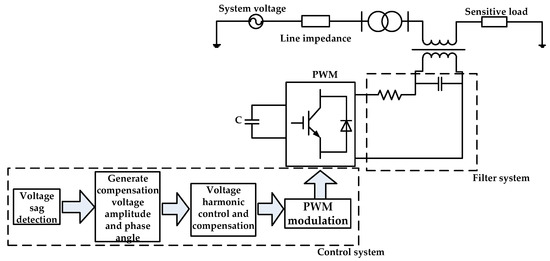
Figure 1.
Dynamic voltage restorer (DVR) compensation schematic.
The main aspects in the research field of DVR include the DVR topology [6,7,8], the location of the output filter capacitance [9], the series transformer’s capacity [10], the control strategies [11,12], the voltage detection methods [13], and the compensation strategies [14]. The studies about the DVR control strategies [11,12] mainly focus on how to improve DVR dynamic performance and harmonic control. The studies about the compensation strategies [14] mainly focus on how to generate the appropriate reference signal economically and effectively. Plenty of researches concentrate on the DVR compensation strategies. Among them, presag compensation, in-phase compensation, and minimum energy compensation are mainly employed [15,16]. The above compensation strategy referenced focus on how to minimize the storage capacitance capacity and increase the DVR effective duration. A new compensation strategy that is based on the combination of minimum energy compensation method and the longest compensation duration method is proposed [17]. The simulation results prove that this compensation strategy can provide compensation of a longer time under the limited energy storage capacity, but the strategy put forward higher requirements on the detecting speed and the accuracy of the equipment. In [5], the compensation voltage vector of DVR is represented by polarization ellipse parameters, and the most effective voltage compensation strategy with the minimum DVR capacity can be achieved by partially optimizing the direction of compensation voltage. However, the compensation to the jumping voltage phase angle of the sensitive load is not considered in the strategies that are mentioned above. For such a situation, a new DVR optimization compensation strategy is proposed in [18], by designing the DVR transition process compensation. As a result, the voltage phase of the sensitive load is compensated, and the compensation time is also significantly increased. Table 2 shows the comparison between the state-of-the-art compensation methods. At present, the researches on DVR compensation strategies focus on the elimination of phase angle jump and the reduction of energy storage capacity to decrease the DVR investment cost. The possible effect of DVR action on adjacent loads has not been studied.
Table 2.
Comparison between the other state-of-the-art compensation methods.
The current research on DVR compensation strategy focuses on how to better improve the compensation capability and the compensation duration for the voltage sag on the sensitive load, but the impact caused by DVR action on the parallel load, named as the adjacent load thereinafter, to the sensitive load at the same busbar has been rarely investigated so far. When a voltage sag occurs in main gird, DVR as an additional source to compensate the voltage for the sensitive load, might cause secondary impacts on the adjacent load. The adjacent load, in turn, might impair the efficiency of DVR in some unfavourable scenarios. The expected influences of DVR on the adjacent load will be pursued as possible, and in which DVR compensation strategies might play an important role. Therefore, the mechanism of the influence of DVR on the adjacent load is worth studying. Besides, when using DVR to mitigate voltage sags, there is an inevitable controversial issue among users who install DVR and those who do not. A more transparent and fairer method in the economic aspect is proposed to address the issue, which is important when the rights of individual users are highly respected nowadays.
In the field of economics, externality, or the spillover effect, reveals that economic activity not only produces the expected effect, but also has certain impact on other parts, except for the main entity in economic activity. This impact is difficult to embody in currency or price in market transactions [19]. Nowadays, the study of externality has covered most economic production activities of the society. The two major problems about externality are how to define externality and how to internalize it [20]. In fact, except for traditional economic activities, some scholars have progressively introduced externality theory into the electrical field. Literature [21] defines energy externality as a kind of transcendence of traditional power systems and it needs to be considered as one of the important problems when constructing new generation of power systems. Literature [22] studies the construction of a new optimal power configuration and externality algorithm based on the externality of communication networks. Literature [23] calculates the external impact of wind power integration on multiple subjects of the power system, and an effective reference is provided for grid operators and in the formulation of subsidies. In the behavior of the DVR compensation for the voltage sag of the sensitive load, the sensitive load is seen as the activity entity, and the adjacent load is the receptor in the whole structure. When the DVR is only carried out compensation when considering the private benefit of the sensitive load, with the presag compensation strategy, for example, the negative externalities or positive externalities might be produced in adjacent loads. In other circumstances when the DVR considers the common interests of the sensitive load and the adjacent load, that is, the normal coordinated strategy to compensate the sensitive load, the compensation effect of the sensitive load itself will be reduced.
From the perspective of traditional equivalent circuit analysis, this paper firstly explores the influence of DVR on adjacent load that is based on the parameters change of network. Subsequently, combined with the theory of externality, a new concept of the first event circle (FEC) is proposed and the externality boundaries are clearly defined when considering network parameters to handle the controversy caused by DVR action among multi entities. Finally, an optimization compensation strategy of DVR based on externality is proposed to ensure different entities’ benefits, and the feasibility and effectiveness of the proposed method is verified by simulation in the MATLAB/Simulink platform.
2. Analysis of Influence of DVR on the Adjacent Load
Figure 2 illustrates the equivalent circuit diagram of the DVR, sensitive load, and adjacent load in order to theoretically analyze the influence of DVR on adjacent load. DVR is regarded as a series voltage source. When there is no voltage sag problem, the switch S closes, and the DVR is standby mode.
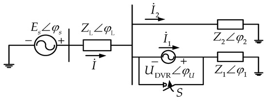
Figure 2.
Equivalent circuit of DVR-sensitive load structures with the adjacent loads; is an infinite system source, regarded as a constant; is the compensation voltage of the DVR; is the line impedance; is the sensitive load impedance; is the adjacent load impedance; are normal running currents of the sensitive load and the adjacent load respectively before voltage sag; and, is the current provided from the source to the loads in normal operation.
When a voltage sag occurs in the infinite system, the monitoring device of DVR triggers to open the switch S, and the DVR outputs the voltage needed. At this time, there are two sources to supply voltage, i.e., the system source and the DVR. The circuit is divided into two parts, according to the superposition theorem for this linear system in the study, as shown in Figure 3 and Figure 4, respectively.
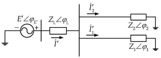
Figure 3.
Equivalent circuit when the system source acts alone; is the grid voltage after the voltage sag occurs, are the currents of the sensitive load and the adjacent load respectively without DVR after voltage sag, is the current supplied by the system source to the loads after voltage sag.
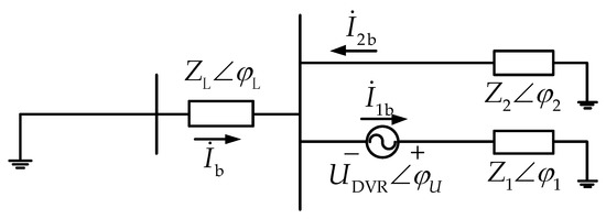
Figure 4.
Equivalent circuit when DVR acts alone; are the compensation currents of the sensitive load and the adjacent load, respectively, provided by DVR after the voltage sag, is the compensation current distributed by the DVR to the other branches in the system, here means the branch to which the original source belong.
The following relationship is obtained, according to the current distribution principle:
where the ratio .
In order to simplify the Equation (1), the distribution coefficient k is defined:
where p is the amplitude of k; is the phase angle of k.
Substitute (2) into Equation (1), then
Meanwhile, k is rationally treated, and expressed into a general plural form, as follows:
It shows that k is dependent on the complex impedance of the transmission line and the complex impedance of the adjacent load. The value of k has the following three cases:
(1) k closes to 1 when x approaches zero, meaning is much smaller than . At this case, the might be close to . As the reference direction of the compensation current provided by DVR is opposite to the reference direction of the adjacent load current itself, the existence of compensation current may cause the adjacent load current drop again (secondary current drop) or rise after the first current drop instantaneous response to the voltage sag. The extent of this subsequent current rise or secondary current drop depends on the size of x.
(2) k is a complex number whose real part is less than 1 when x is set as constant , meaning , and the compensation current of the adjacent load can be obtained with the scaling and rotating of the sensitive load compensation current. There is still a secondary current rise or secondary current drop of the adjacent load for this case.
(3) k approaches 0, when x tends to infinity, meaning that can be ignored. In this case, also closes to 0. For the DVR-sensitive load structure with adjacent load, the influence of the DVR on the adjacent load is generally effective, since the equivalent system line impedance is always large enough to be considered in a real case. The larger the k is, the more influence of the DVR on the adjacent load will be.
In the circumstance where the system structure parameters are given, the magnitude and phase angle of the is affected by , and the amplitude of depends on the magnitude and phase angle of the DVR compensation voltage. How the DVR compensation voltage affects the adjacent load behavior in terms of current change with different would be addressed by the phasor diagram. The phasor diagram analysis can simplify the complex theoretical analysis into an intelligible phasor analysis and it is widely used in the analysis of DVR compensation strategy regarding the DVR compensation strategy [5,17,24,25]. The analysis of different is shown, as follows:
(A) When the impedance of the sensitive load is different from that of the adjacent load, namely , as shown in Figure 5.
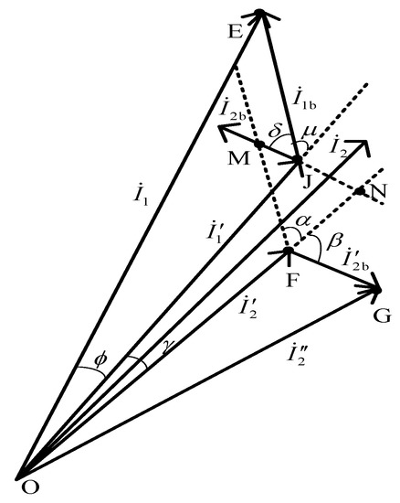
Figure 5.
Phasor diagram of the influence of DVR on the adjacent load current.
In Figure 5, as is opposite to in the direction, when solving the secondary current change of the adjacent load , it is necessary to move along the reverse direction and parallel to the point F to obtain . In this diagram, the angle between and is defined as . The angle between and is defined as . In , , and , with is to be searched. and can be obtained by the solution of , and is the angle between the adjacent load current and the sensitive load current after the voltage sag occurs, which can be obtained by the measuring device of DVR. From Figure 5, it can be seen that the adjacent load current change highly depends on the relation of the impedance of the sensitive load and that of the adjacent load.
(B) For simplification, while assuming , the corresponding phasor diagram is shown in Figure 6. The phasor like in the Figure 6 means that and are equal. Noticeably, the analysis in Section 3 is based on the assumption .
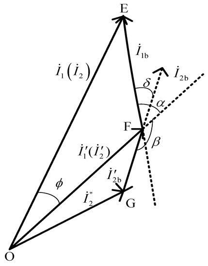
Figure 6.
Phasor diagram of the influence of DVR on the adjacent load current when .
Taking the classical presag compensation strategy of DVR as an example, the corresponding conditions for the secondary current drop, secondary current rise, or keeping current constant for adjacent load are deduced, as follows.
As the reference direction of the compensation current for the adjacent load is opposite to the original current reference direction of the adjacent load, one can obtain
In Figure 3, it is shown that is rotated 180 degrees counterclockwise around point F and is then summed with to obtain . The Equations (6) and (7) can be deduced, referring to Figure 4 and Figure 5 as
When the secondary current drop of adjacent load occurs:
Substitute the Equations (6) and (7) into (8), then
Finally:
Similarly, if secondary current rises with DVR action after voltage sag and the adjacent load current amplitude is kept unchanged, (11) and (12) can be determined, respectively.
In Equations (10)–(12), except for the amplitude and phase angle of , other variables can be obtained in given real cases. By controlling the amplitude and the phase angle of , the influence of DVR on the adjacent load in terms of current change could be estimated and directed based on different strategies.
3. Definition of Externality
3.1. Judgment of the Nature of Externality
Generally, according to whether the influence caused by the activity harms the interests of others or not, the externality is divided into positive externality and negative externality, as shown in Figure 7.
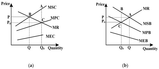
Figure 7.
Externality schematics: (a) Negative externality, MSC represents marginal social cost, MPC represents marginal private cost, MR represents marginal requirement, and MEC represents marginal external cost. (b) Positive externality, MSB represents the marginal social benefits, MPB represents the marginal private benefits, and MEB represents the marginal external benefits.
In Figure 7a, point C means the economic activity entity conducts economic activities according to marginal private cost (MPC). However, when the activity entity conducts activities, having a negative externality to other entities, a MEC is appearing. From the perspective of the whole society, the production cost of the activity entity is no longer the MPC, but the marginal social cost (MSC). The intersection of MSC and demand curve (point B in Figure 7a) is the social optimal value in this case. The product cost price at point B is larger than P0, and the output Q is less than Q0, which means that the production output is too much due to externalities, and the society also bears part of the cost loss, which makes the product cost lower. In Figure 7b, point C means the activity entity conducts activities according to marginal private benefits (MPB). As the social benefit marginal social benefits (MSB) is greater than MPB, the intersection of MSB and demand curve (point A in Figure 7b) is the social optimal value in positive externality circumstance. It can be seen that at the optimum of society output Q is greater than the output Q0. In Figure 7a,b, due to the increase in the cost price P, it is difficult for the activity entity to spontaneously arrange production activities from the perspective of the whole society.
The above analysis indicates that there are three possible cases of DVR affecting the adjacent load, representing positive, negative, and no externality. The externality theory is introduced in order to better analyze these three cases. In this paper, the way to solve the external problem of DVR is to set the appropriate compensation mechanism, combined with the actual situation in China. Coase’s property right definition theory is not very applicable in China at present, so “Pigovian tax” is employed as the theoretical basis for our design of compensation mechanism. When using the “Pigovian tax” method, firstly we must determine the externality accepting entity and release entity, and then design the compensation mechanism according to the principle of “who compensates who benefits” and “who pollutes who manages” [26,27]. When the voltage sag occurs, the external release entity in this paper is DVR at the sensitive load branch, while the accepting entity is the adjacent load. The magnitude of the externality w can be generally embodied in electric field by relative vectors, such as current, voltage, and so on. The quantitative definition of the externality w is described in the below section.
As shown in Figure 8, we define two current circles in phasor diagram: one is the normal running circle (NRC), with the amplitude of the sensitive load current during normal operation as the radius, namely , another circle is the FEC, and the amplitude of the sensitive load current after the voltage sag occurs is the radius, namely . On this basis, FEC is used as the boundary between positive and negative externalities, and the criteria for defining externalities. as follows:
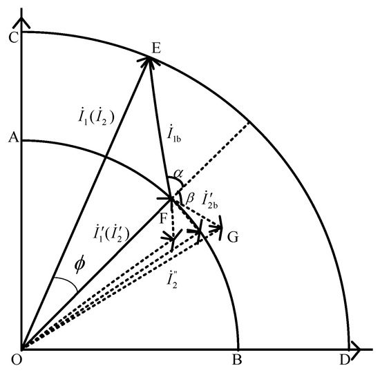
Figure 8.
Phasor diagram of DVR’s externality.
a. when , the DVR has positive external influence on adjacent load;
b. when , the DVR has a negative external influence on the adjacent load; and,
c. when , the DVR has no external influence on the adjacent load, and the ideal case is that only the phase angle of changes with the amplitude fixed.
The externality is defined as w, and its expression is as follows:
3.2. The External Compensation Range
The following discussion is based on the hypothesis that the DVR energy storage can realize the in-phase compensation strategy at least, which means that the dotted circle in Figure 9 can intersect with arc CD. When the resulting current of the sensitive load and adjacent load drop to ( in Figure 9) due to the system voltage sag, the DVR acts to compensate the voltage sag, which provides a compensation current called ( in Figure 9) for the sensitive load. The compensation of the DVR returns the sensitive load to the normal current level; at the same time, the compensation current, called ( in Figure 9), is also provided for the adjacent load, so that the adjacent load current drops again to ( in Figure 9).
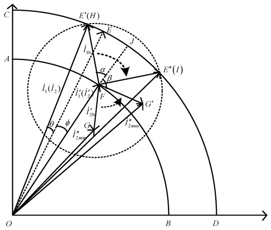
Figure 9.
Phasor diagram of the external compensation range.
In phasor diagram analysis of the traditional DVR compensation strategy, in order to represent the DVR compensation capability limit, the concept of DVR compensation voltage limit circle (CVLC) is often cited [28]. Correspondingly, the concept of DVR compensation current limit circle (CCLC) is created in this paper. The point F, as the phasor end of sensitive load current after the voltage sag, is set as the center of the circle, and the DVR limit compensation current amplitude is the radius, and then a dotted circle is made, as shown in Figure 9. The circle is defined as the CCLC, with the limit compensation current is calculated, as follows:
In Equation (14), is the limit compensation voltage amplitude of the DVR. The CCLC intersects the arc CD of NRC at points H and I, in which the boundary of would be found as follows.
During this voltage sag, is given according to real grid situation and can be regarded as constant. Each of varies with , where is determined by the DVR’s compensation strategy. The amplitude range of is . , and the phase angle α varies from , where J is the intersection of the current () extension line and the NRC after voltage sag. If the compensation current is turned to the J point, the magnitude of the compensation current is the smallest, which in fact refers to the in-phase compensation strategy. The phasor diagram that is shown in Figure 9 shows that, when the compensation current is limited to the arc HJ, it is necessary to use for determining the phase angle α of . First of all, by the cosine theorem, the rotation angle of , , is
in the range of . It is easy to know from Equation (15) that monotonously increases as increases. Similarly, we can obtain the complementary angle of ∠EFO of , α, as
where β is the complementary angle of ∠OFG, and the value of ∠OFG can be obtained by solving β. It is easy to know that α increases with . Figure 6 shows the relationship between α and β, as follows,
It can be seen from Equation (2) that δ is a phase angle that is determined by a given complex number k, and then combined ∆OFG with (3), the result is
Let , , Equation (18) becomes:
where only n, m is unknown. It shows that for n in anywhere between , m is a monotonically increasing function with respect to n. Let n take the maximal , then , namely when in Figure 9 is rotated to H, gets the maximum value. Similarly, a similar geometric analysis can be conducted to know that, when the compensation current is limited to the arc JI, , namely when in Figure 9 is rotated to I, is minimal. Thus, the upper and lower limits of is obtained in general. The nature of DVR’s externality, no, positive and negative, could be discriminated by checking the externality of the two intersection points (H,I). In this paper, the range of the externality w, , is set to correspond to the range of .
In the above analysis, only the situation when the angle of and is an obtuse angle is discussed. Similarly, if the angle of and is arbitrary, the similar analysis by phasor diagram can be used to obtain a function relationship between and . The compensation range of from the expected compensation strategies can determine the variance of , and then the range of can be calculated with Equation (18), and so does the externality w.
3.3. Compensation Costs for Externalities
When the DVR’s externality on the adjacent load is not completely internalized, no matter positive or negative, the DVR owner (the sensitive load is the DVR’s owner in this paper) or the adjacent load is compensated by the grid with “Pigovian tax” in this paper. The externality w is defined as the compensation power of the adjacent load , from the DVR.
Correspondingly, is the sensitive load compensation power from the DVR.
In order to quantify the impact of externality and compensate the DVR owner, the DVR full-life cost model [29] is proposed, as follows:
Equations (22) and (23) assume that is the total cost for the entire life cycle of the DVR, consisting of three parts: installation cost , maintenance cost , and operating cost . is the discount rate, T is the engineering life, t is the year of use, and q is the number of times when the DVR compensation amplitude reaches 100% after the voltage sag in the entire life cycle of the DVR. is the cost of each voltage sag compensation action. Then we can calculate the economic cost of externality in each DVR compensation process:
The current ratio in the Equation (24) represents the degree of decrease in current relative to the normal operating current during sag, and it is used to represent the severity of the accident.
4. Design of DVR Optimization Compensation Strategy Considering Externality
Before the optimization compensation strategy is proposed, several hypotheses for the establishment of the strategy need to be explained:
- The proposed compensation strategy in this paper is only applicable to the optimization of fundamental signal.
- The line impedance should not be ignored, otherwise the externalities will be very small, and the compensation strategy of DVR should not take the possible externalities on adjacent loads into a consideration.
- The externalities of the DVR on adjacent loads can only be discussed if the equivalent circuit structure shown in the Figure 2 is satisfied.
According to the previous section, the range of the externality on the adjacent load that is caused by DVR compensation will be obtained with the sag current of the sensitive load, the sag current of the adjacent load and DVR compensation limit determined by its capacity. Figure 10 shows the optimized compensation strategy to minimize the externality.
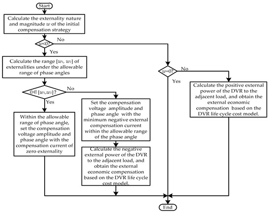
Figure 10.
Flow chart of optimized compensation strategy.
In Figure 10, If the condition w < 0 is not met, it indicates that the externality of the initial compensation strategy is non-negative, and the compensation costs will be given to the DVR owner directly, and there is no need to further optimize the compensation strategy. If the judgment w < 0 is yes, then the initial compensation strategy needs to be optimized. Subsequently, if is not true, this means that even the pursuing optimization strategy cannot achieve no or positive externality, thus the target is to achieve the minimum negative externality as much as possible.
Immediate compensation is not suitable for the single external economic compensation payment in the flow chart due to its small value. Instead, the grid operator will offer compensation to the DVR owners as soon as the cumulative external economic compensation reaches a certain value. If the externality is positive, the grid operator will reward the DVR owners; conversely, if the externality is negative, the network operator will punish the DVR owners with “Pigovian tax” and compensate the adjacent load of DVR at the same time. The compensation that is caused by negative externality is marked as a negative value, and the compensation that is related to the positive externality is considered to be positive.
Potentially, different compensation ranges might result in scalable externality, but the calculation process is consistent. Taking Figure 9 as an example, the computational complexity of the model is analyzed. According to Figure 11, the whole calculation model is divided into two parts: calculation of external compensation range and calculation of external costs. The calculation model does not involve iteration process, but it mainly involves algebraic calculation and a large number of trigonometric function’s operations. When compared with the traditional compensation strategies, the proposed optimization strategy only increases the calculation of some algebraic equations. Its computational complexity and calculated time are controllable, which is within the acceptable range of real projects.
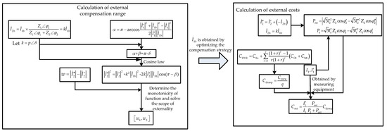
Figure 11.
The calculation flow chart of the calculation model.
5. Simulation Results
5.1. Construction of the Simulation System with DVR and Loads
The proposed method is checked in the simple system of small-capacity shown in the Figure 2, which is constructed in MATLAB/Simulink platform. The DVR compensation effect can be analyzed by imitating just single-phase DVR compensation, as that most of the DVRs currently used are of single-phase full-bridge inverter structure. The initial parameters of the test system are given by Table 3. The allowable phase angle offset of the sensitive load is set to [−5°, 5°]. It is assumed that the voltage sag in the system occurs 100 times in one year, with a fixed duration of 80ms each time. The extent of amplitude decrease are 25% (50 times), 50% (30 times), and 75% (20 times) respectively, and the drop phase angles are −30° (- means decrease), −20°, and −10°, respectively.
Table 3.
Simulation parameters of system with DVR
5.2. Externalities Analysis Considering Impedance Ratio k and z1/z2 Change
According to the analysis in the second section, the externality caused by DVR compensation to the adjacent loads depends on the impedance ratio k and the sensitive load and the adjacent load impedance ratio . For comparison, three cases are tested for th presag compensation strategy.
Case 1 uses the parameters of Table 3. The parameters of case 2 is the same as case 1, except , meaning that the size of sensitive load is 10 times that of the adjacent load. Case 3 adapts the k to 0.5 times of the default value in case 1 with other parameter unchanged. The most often happening situation of 25% voltage sag is taken as an example. Besides, assume that the line impedance and the sensitive load impedance are fixed, and only the adjacent load impedance is variable. Figure 12 shows the simulation results.
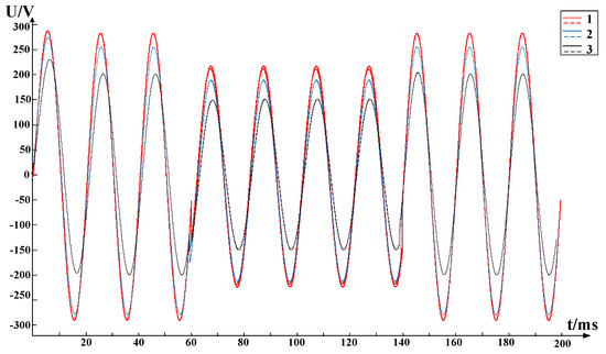
Figure 12.
Comparison of adjacent load voltages of three cases.
In Figure 12, the voltage sag occurs from 60 ms to 140 ms. The solid line indicates the adjacent load voltage with DVR compensation, and the dashed line represents the adjacent load voltage without DVR. The externality effect of case 1 is more obvious than cases 2 and 3, and the dashed line and the solid line of cases 2, 3 almost completely overlaps. We zoom in the part of the curve in Figure 11 from 85 ms to 90 ms to manifest the difference of cases, as shown in Figure 13.
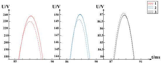
Figure 13.
Adjacent load voltages of 3 cases from 85 ms to 90 ms.
Figure 13 shows that cases 1 and 2 have positive externalities on the adjacent load, while case 3 is of negative externality. In case 1, the DVR in the presag compensation strategy resulted in the adjacent load voltage a secondary rise of 6.1V. In case 2, only a secondary voltage rise of 0.5V was found for the adjacent load. As to case 3, a secondary voltage drop of 0.3V was imposed in the adjacent load.
It can be seen that, sometimes, the single impact of the DVR on the adjacent load is relatively small, but not negligible. This paper counts the DVR externality compensation cost for voltage sag in 100 times accumulated per year, and Table 4 shows the results:
Table 4.
Comparison of external cost caused by DVR action within one year.
The sign in brackets following the data in the table only means the resulting externality nature, positive or negative. In most cases, the externality influence of the DVR on the adjacent load is negative, and the result of case 3 clarifies that the external influence will be weakened with a decreasing k. On the basis of a conservative estimation that the voltage sag accidents only happen 100 times a year, the DVR causes a non-negligible economic loss to the adjacent load. It should be noted that the load capacity of the test system in this paper is small, hence the external compensation cost is also not obvious. However, in the industrial parks with having high-quality power requirement, the capacity of the DVR and the system are probable both at the MVA level. The compensation cost counted due to the externality is magnified several tens of times of this case and it surely cannot be ignored.
5.3. Optimization Compensation Strategy Analysis
A comparison between the externality minimum compensation strategy (Optimized) and the traditional presag compensation strategy (Normal) will be presented in this part to verify the effectiveness of the optimized compensation strategy. According to the above section, when the traditional presag compensation strategy is adopted, the DVR compensation shows positive externality in a 25% voltage sag case. In this occasion, the economic compensation is directly carried out according to the rule suggested. However, when 50% and 75% voltage sag accidents occur, the DVR compensation results are a negative externality to the adjacent load. At this time, the proposed externality minimum compensation strategy is applied to reduce the negative externalities. Take the 50% voltage sag as an example, and the results are shown in Figure 14 and Figure 15.
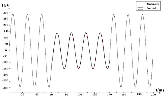
Figure 14.
Comparison of adjacent load voltage waveforms for different strategies at 50% voltage sag.
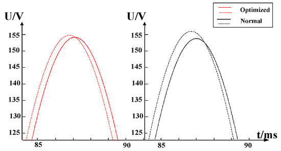
Figure 15.
Partial enlargement of Figure 14 from 85ms to 90ms.
According to the calculated results, with a −20° phase angle offset and a 50% voltage sag, the influence of the DVR on the adjacent load always appears as a negative externality within the allowable phase angle deviation range. In addition, the negative externality is minimal when the offset phase angle is −5°. In Figure 14, the voltage curves of the two compensation strategies almost coincide, because the optimization compensation strategy is based on the fine adjustment of the presag compensation strategy. A partially enlarged version (Figure 15) of Figure 14 gives more detailed information in order to illustrate the similarities and differences of the compensation strategies more clearly. It can be concluded that the optimized compensation strategy reduces the negative externality to a certain extent when compared to the normal presag compensation strategy.
Table 5 indicates that considering a given allowable phase offset range of the sensitive load, the optimized compensation strategy can significantly reduce the economic loss of the adjacent load that was caused by the DVR compensation. If it is the case that the sensitive load in this paper only need to compensate for the voltage amplitude without requirement on the phase angle, the DVR compensation capability is determined by just the phase angle to offset range permitted, which might realize better compensation result with less cost. For such a case, the simulated results are shown in Table 6.
Table 5.
Comparison between optimized compensation strategy and presag compensation strategy.
Table 6.
Comparison of optimized compensation strategy and presag compensation strategy when phase angle jump compensation is not required.
Referring to Table 6, if the DVR capacity is large enough and the sensitive load does not have any requirement for the phase angle offset, the optimized compensation strategy can achieve no externality as possible and positive externality if it can not realize any externality.
6. Conclusions
This paper deals with the externality of the influence of DVR on the adjacent load and then introduces the FEC and CCLC in phasor diagram for quantification analysis. As a result, the positive externality, the negative externality, and no externality are found and are described based on the system configuration parameters. The existence of externalities causes “free-riding” between adjacent loads and sensitive loads. An external optimization compensation strategy is presented and verified by simulation in order to serve a clue for solving such kind problems.
The findings are as followings:
- (1)
- The impact of DVR on adjacent load does exist and will become more and more obvious in the future. This will probably result in disputes between electric energy users, which is not conducive to the popularization and promotion of DVR equipment.
- (2)
- Transforming the influence of DVR on adjacent load into a model of externality is beneficial to distinguish the interaction between different entities. Referring to the classical solution of external problems, this paper classifies the externality of DVR on adjacent load and deduces the corresponding existence conditions. An optimization compensation strategy is proposed to reduce the compensation cost and the effectiveness of the proposed method is verified by simulation in a simple test system in the MATLAB platform.
The main disadvantage of the proposed method is that it will greatly increase the computational difficulty in operation scenarios with many adjacent loads. Clustering equivalence of adjacent loads might be a solution to this problem. In the future, more detailed economic cost analysis based on externality can be considered for the structure of multi sensitive loads and multi adjacent loads. Additionally, the power quality equipment configuration and optimization would be investigated with the implementation of the solution strategy.
Author Contributions
Conceptualization, Z.D., Z.C. and G.D.; methodology, Z.D. and Z.C.; software, G.D.; validation, Z.D., M.Y.J. and C.S.; formal analysis, Z.D.; data curation, Z.C.; writing—original draft preparation, Z.D. and Z.C.; writing—review and editing, M.Y.J., H.Z. and C.S.
Funding
The research work is supported by the National Natural Science Foundation of China under Grant no. 51761145106.
Conflicts of Interest
The authors declare no conflict of interest.
References
- Bollen, M.H.J. Understanding Power Quality Problems, Voltage Sags and Interruptions; IEEE Press: New York, NY, USA, 2000. [Google Scholar]
- Steciuk, P.B.; Redmon, J.R. Voltage sag analysis peaks customer service. IEEE Comput. Appl. Power 1996, 9, 48–51. [Google Scholar]
- Gomez, J.C.; Morcos, M.M. Voltage Sag and Recovery Time in Repetitive Events. IEEE Trans. Power Deliv. 2002, 17, 1037–1043. [Google Scholar] [CrossRef]
- Yang, Y.; Xiao, X.; Guo, S.; Gao, Y.; Yuan, C.; Yang, W. Energy Storage Characteristic Analysis of Voltage Sags Compensation for UPQC Based on MMC for Medium Voltage Distribution System. Energies 2018, 11, 923. [Google Scholar] [CrossRef]
- Li, P.; Xie, L.; Han, J.; Pang, S.; Li, P.A. New Voltage Compensation Philosophy for Dynamic Voltage Restorer to Mitigate Voltage Sags Using Three-Phase Voltage Ellipse Parameters. IEEE Trans. Power Electron. 2018, 33, 1154–1166. [Google Scholar] [CrossRef]
- Jiang, F.; Tu, C.; Shuai, Z.; Cheng, M.; Lan, Z.; Xiao, F. Multilevel Cascaded-Type Dynamic Voltage Restorer with Fault Current-Limiting Function. IEEE Trans. Power Deliv. 2016, 31, 1261–1269. [Google Scholar] [CrossRef]
- Kim, S.; Kim, H.-G.; Cha, H. Dynamic Voltage Restorer Using Switching Cell Structured Multilevel AC-AC Converter. IEEE Trans. Power Electron. 2017, 32, 8406–8418. [Google Scholar] [CrossRef]
- Zhou, M.; Sun, Y.; Su, M.; Li, X.; Lin, J.; Liang, J.; Liu, Y. Transformer-less dynamic voltage restorer based on a three-leg ac/ac converter. IET Power Electron. 2018, 11, 2045–2052. [Google Scholar] [CrossRef]
- Choi, S.S.; Li, B.H.; Vilathgamuwa, D.M. A comparative study of inverter- and line-side filtering schemes in the dynamic voltage restorer. In Proceedings of the 2000 IEEE Power Engineering Society Winter Meeting. Conference Proceedings, Singapore, 23–27 January 2000. [Google Scholar]
- Majchrzak, V.; Parent, G.; Brudny, J.-F.; Costan, V.; Guuinic, P. Design of a Coupling Transformer with a Virtual Air Gap for Dynamic Voltage Restorers. IEEE Trans. Magn. 2016, 52, 8401104. [Google Scholar] [CrossRef]
- Tien, D.V.; Gono, R.; Leonowicz, Z. A Multifunctional Dynamic Voltage Restorer for Power Quality Improvement. Energies 2018, 11, 1351. [Google Scholar] [CrossRef]
- Roldan-Perez, J.; Garcia-Cerrada, A.; Rodriguez-Cabero, A.; Luis Zamora-Macho, J. Comprehensive Design and Analysis of a State-Feedback Controller for a Dynamic Voltage Restorer. Energies 2018, 11, 1972. [Google Scholar] [CrossRef]
- Sadigh, A.K.; Smedley, K.M. Fast and precise voltage sag detection method for dynamic voltage restorer (DVR) application. Electr. Power Syst. Res. 2016, 130, 192–207. [Google Scholar] [CrossRef]
- Farhadi-Kangarlu, M.; Babaei, E.; Blaabjerg, F. A comprehensive review of dynamic voltage restorers. Int. J. Electr. Power Energy Syst. 2017, 92, 136–155. [Google Scholar] [CrossRef]
- Biricik, S.; Komurcugil, H.; Tuyen, N.D.; Basu, M. Protection of Sensitive Loads Using Sliding Mode Controlled Three-Phase DVR with Adaptive Notch Filter. IEEE Trans. Ind. Electron. 2019, 66, 5465–5475. [Google Scholar] [CrossRef]
- Tu, C.; Sun, Y.; Guo, Q.; Fei, J.; Li, Z. The Minimum Energy Soft-Switching Control Strategy for Dynamic Voltage Restorer. Trans. China Electrotech. Soc. 2019, 34, 3035–3045. [Google Scholar]
- Rauf, A.M.; Khadkikar, V. An Enhanced Voltage Sag Compensation Scheme for Dynamic Voltage Restorer. IEEE Trans. Ind. Electron. 2015, 62, 2683–2692. [Google Scholar] [CrossRef]
- Domijan, A.; Montenegro, A.; Keri, A.J.F.; Mattern, K.E. Simulation Study of the World’s First Distributed Premium Power Quality Park. IEEE Trans. Power Deliv. 2005, 20, 1483–1492. [Google Scholar] [CrossRef]
- James, M. Buchanan and Wm. Craig Stubblebine. Externality. Economica 1962, 29, 371–384. [Google Scholar]
- Rochet, J.C.; Tirole, J. Two-sided markets: a progress report. RAND J. Econ. 2006, 37, 645–667. [Google Scholar] [CrossRef]
- O’Neill-Carrillo, E.; Zamot, H.R.; Hernández, M.; Irizarry-Rivera, A.A.; Jiménez-Rodríguez, L.O. Beyond traditional power systems: Energy externalities, ethics and society. In Proceedings of the 2012 IEEE International Symposium on Sustainable Systems and Technology, Boston, MA, USA, 16–18 May 2012. [Google Scholar]
- Kallitsis, M.G.; Michailidis, G.; Devetsikiotis, M. Optimal Power Allocation Under Communication Network Externalities. IEEE Trans. Smart Grid 2012, 3, 162–173. [Google Scholar] [CrossRef]
- Huiru, Z.; Sen, G.; Hongze, L. Economic Impact Assessment of Wind Power Integration: A Quasi-Public Goods Property Perspective. Energies 2015, 8, 8749–8774. [Google Scholar]
- Li, P.; Xie, L.; Han, J.; Pang, S.; Li, P. New Decentralized Control Scheme for a Dynamic Voltage Restorer Based on the Elliptical Trajectory Compensation. IEEE Trans. Ind. Electron. 2017, 64, 6484–6495. [Google Scholar] [CrossRef]
- Jayaprakash, P.; Singh, B.; Kothari, D.P.; Chandra, A.; Al-Haddad, K. Control of Reduced-Rating Dynamic Voltage Restorer with a Battery Energy Storage System. IEEE Trans. Ind. Appl. 2014, 50, 1295–1303. [Google Scholar] [CrossRef]
- De Borger, B.; Glazer, A. Support and opposition to a Pigovian tax: Road pricing with reference-dependent preferences. J. Urban Econ. 2017, 99, 31–47. [Google Scholar] [CrossRef]
- Robson, A.; Skaperdas, S. Costly enforcement of property rights and the Coase theorem. Econ. Theory 2008, 36, 109–128. [Google Scholar] [CrossRef]
- Sun, Z.; Guo, C.; Xiao, X.; Xu, Y.; Liu, Y. Analysis Method of DVR Compensation Strategy Based on Load Voltage and Minimum Energy Control. Proc. CSEE 2010, 30, 43–49. [Google Scholar]
- Zheng, Z.; Li, Y.; Xie, X.; Zheng, Y.; Zhang, Z.; Ai, Q. Allocation plan of voltage sags mitigation devices based on life cycle cost. Power Syst. Prot. Control 2018, 46, 128–134. [Google Scholar]


© 2019 by the authors. Licensee MDPI, Basel, Switzerland. This article is an open access article distributed under the terms and conditions of the Creative Commons Attribution (CC BY) license (http://creativecommons.org/licenses/by/4.0/).