Abstract
The aging fracture of bonding wire is one of the main reasons for failure of insulated gate bipolar transistor (IGBT). This paper proposes an online monitoring method for IGBT bonding wire aging that does not interfere with the normal operation of the IGBT module. A quantitative analysis of aging degree was first performed, and the results of multivariate and univariate monitoring were compared. Based on the relationship between the monitoring parameters and the aging of the IGBT bonding wire, gradual damage of the IGBT bond wire was implemented to simulate aging failure and obtain the aging data. Moreover, the change of junction temperature was considered to regulate monitoring parameters. Then, the aging degree was evaluated by an artificial neural network (ANN) algorithm. The experimental results showed the effectiveness of the proposed method.
1. Introduction
In modern industrial systems, power semiconductor devices have become increasingly indispensable. They are widely used in electric locomotive traction, aerospace, industrial automation, transportation, new energy generation, and so on. Power switching devices as the core components of electronic devices are becoming increasingly important [1,2,3]. Among them, insulated gate bipolar transistors (IGBTs) are the most widely used power switching devices in the industrial field. As one of the most inefficient devices in power converters [4,5], IGBT failure is mainly caused by the breakage and shedding of bond wires due to aging [6]. In order to improve the reliability of power converters, it is necessary to monitor the state of the IGBT module and study the aging process.
The health management and condition monitoring methods for IGBTs have been widely studied and discussed. The mainstream research can be divided into two categories. The first category is IGBT life assessment technologies. Here, life analysis models, such as the Coffin–Manson model [7], the Norris–Landzberg model [8], and the Bayerer model [9], have been proposed. In addition, physical models of finite element simulation analysis based on different physical properties of materials have also been proposed to more accurately analyze the change in stress [10]. The second category is the IGBT condition monitoring technologies. Gate voltage oscillations are monitored to analyze the relationship between bond wire degradation and high frequency response. The k-nearest neighbor algorithm based on the cycle aging of power is explored to evaluate its health status through power characteristics such as Vce(on) [11]. Moreover, training data is used to evaluate the weight factor of each feature according to the statistical feature weighting method. The accuracy of the optimized classification is analyzed to estimate the remaining life [12]. In addition, the rupture of the bond wire can be clearly monitored by eddy current pulse thermal imaging, which requires the application of additional measuring equipment on the IGBT module and may affect the normal operation of the IGBT module [13]. The saturation conduction voltage drop Vce-sat [14,15,16] and the bond wire equivalent resistance RJ [17] are also often used for the detection of bond wire shedding as well as monitoring of the IGBT turn-off time as a symptom of the latch-up effect [18]. These techniques cannot quantitatively analyze the loss rate of the IGBT bond wire and may affect the normal operation of the IGBT in the application.
In view of the above discussion, an online monitoring and evaluation method based on multivariable IGBT bond wire aging is proposed in this paper. An IGBT aging test bench and monitoring system was built to realize online evaluation of the aging state of IGBT bond wire. First, the failure mechanism of IGBT was analyzed theoretically. Then, the relationship between IGBT’s conduction voltage drop Vce, Miller platform voltage Vge, Miller platform duration tge, and bond line aging was evaluated. Through the gradual destruction of the IGBT bond wire, the aging failure of the IGBT bond wire was simulated. Meanwhile, Vce, Vge, and tge at different degrees of aging were obtained. Then, the relationship between junction temperature and the three parameters was established through experiments. Junction temperature correction was performed after standardizing the three parameters at different temperatures. Finally, an artificial neural network (ANN) algorithm was used to evaluate and monitor the current aging degree of IGBT bond wires.
2. Characteristics Analysis of IGBT Aging Mechanism
2.1. IGBT Failure Mechanism
The key parameter to assess the degree of system performance degradation is reliability, and the life cycle of a power device is determined by the module failure mechanism. Therefore, the power device failure mechanism is the basis of state evaluation [3].
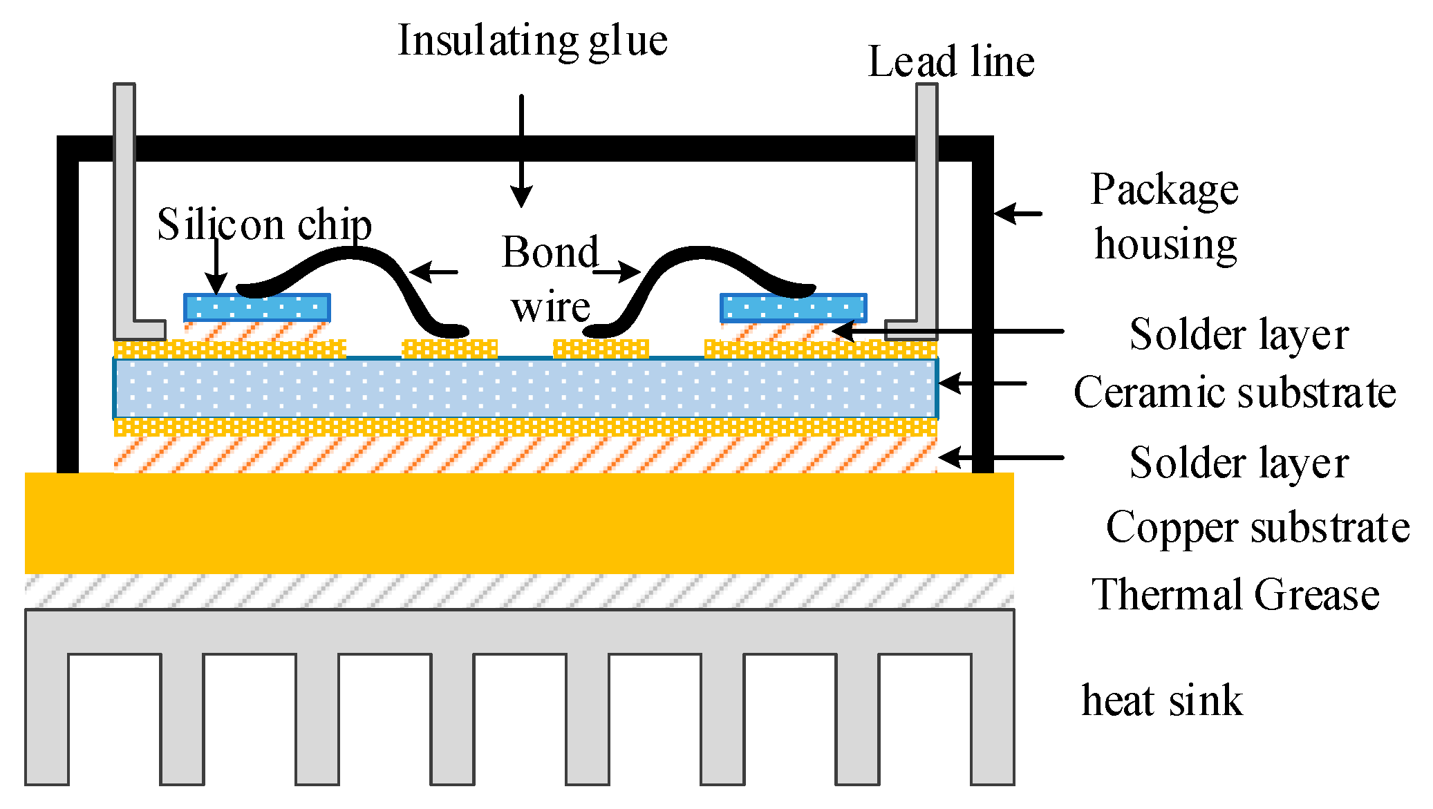
A fully packaged IGBT module is a multilayer structure with different materials packaged together, as shown in Figure 1.
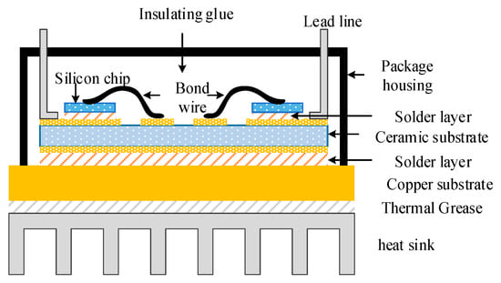
Figure 1.
Diagram of insulated gate bipolar transistor (IGBT) cross-sectional structure.
Each material increases in volume to a certain extent after being heated, also known as thermal expansion. The coefficient characterizing this property is called the coefficient of thermal expansion. Each layer is composed of a different material, and the coefficient of thermal expansion is also different. The difference in thermal expansion coefficient of the aluminum bonding wire and the solder layer is large. In actual work, the on-state loss and switching loss of the IGBT cause the junction temperature of the device to rise. The material of each layer expands, and the device cools to shrink the materials of each layer. Different thermal expansion coefficients lead to different degrees of expansion of different materials during temperature cycling. Therefore, different materials are subjected to different compressive or tensile stresses, so the thermomechanical stress inside the IGBT is generated by the power cycle. These thermal stresses cause repeated impacts on the material joints of the various layers within the IGBT module, especially the bonding of the bond wires to the chip and the solder layer. In the end, the joints, such as the solder layer, the bonding wires, and the terminal pads, are directly damaged, causing fatigue of the solder layer, cracking, crack growth, and even delamination of the layers, voids, and bonding wires, causing the module to fail [19].
2.2. Influence of Aging of IGBT Bond Wire on Turn-On Voltage
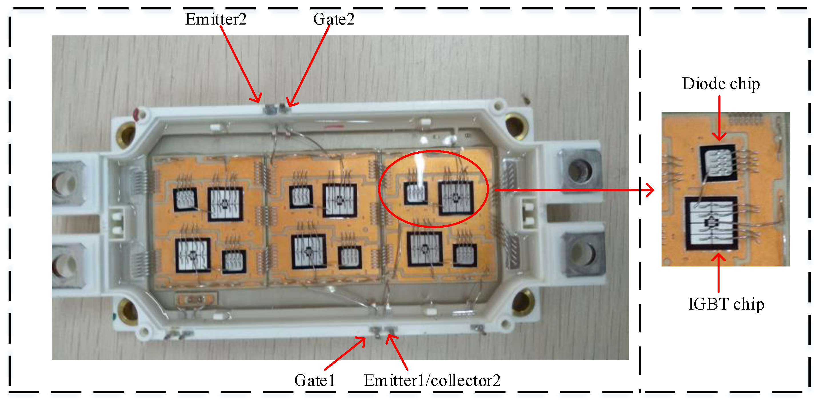
The IGBT module used in this study was Infineon FF225R17ME4. This module is similar to most existing IGBT structures. A diagram of the opened IGBT module is shown below in Figure 2.
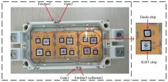
Figure 2.
The opened IGBT module.
The IGBT module comprises a whole IGBT bridge arm and two IGBT submodules. Each submodule has three modules in which one IGBT chip and one diode chip are connected in antiparallel, and each IGBT chip has four bond wires. A direct cutting IGBT bond wire can be used to simulate the aging of IGBT bond wire and ensure an effective simulation of IGBT bond wire failure [20].
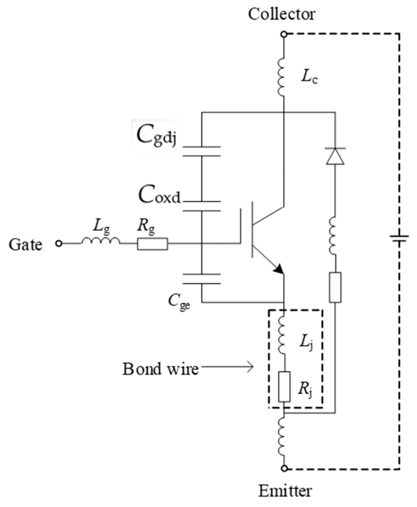
The equivalent circuit diagram of IGBT is shown in Figure 3, where Lj and Rj are the equivalent inductance and resistance of the bonding wire, respectively; Lg and Rg are the gate parasitic inductance and parasitic resistance, respectively; Cge is the gate-emitter parasitic capacitance; and Cgc is the gate-collective parasitic capacitance, where Cgc = Cgdj + Coxd.
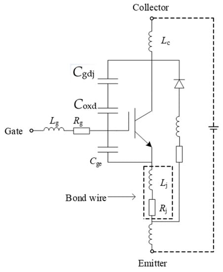
Figure 3.
Equivalent circuit diagram of IGBT.
When the IGBT is fully turned on, the mathematical expression of the turn-on voltage drop Vce is as follows:
The Vpn (pn junction voltage drop of the IGBT) and the Vdrift (conduction voltage drop of the drift region) remain substantially unchanged when the IGBT is fully turned on, and the bond line equivalent resistance Rj gradually becomes larger as the bonding wire ages and breaks. The IGBT turn-on voltage drop rises, with the emitter current Ie not changing.
2.3. Influence of Aging of IGBT Bond Wires on Miller Plateau Voltage and Its Duration
Due to the existence of gate parasitic capacitance, the gate voltage of the IGBT is determined by the charge and gate capacitance, which is given by
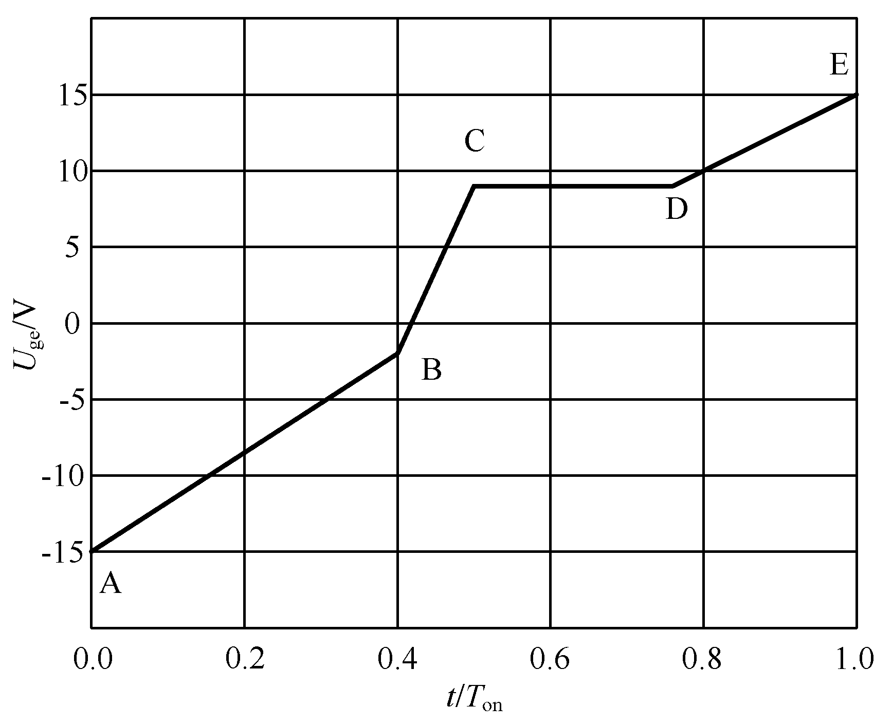
When the IGBT is turned on, the change in gate voltage is not linear but rather a multistage process. The changing process of gate voltage Uge during the turn-on process is shown in Figure 4.
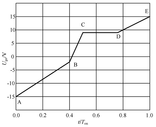
Figure 4.
The gate voltage Uge changing process.
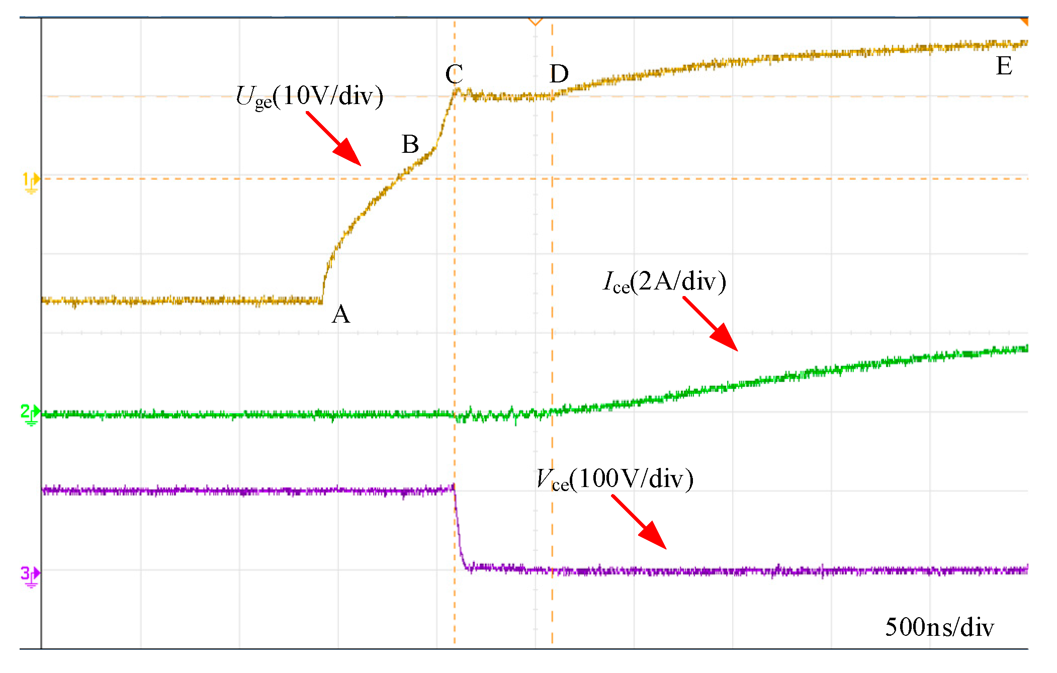
At point A, Uge rises when the gate capacitance Cge is charged, and Uge rises exponentially, affected by the gate capacitance Cge. At point B, Uge reaches the flatband voltage Ufb, and part of the Cge capacitor, called metal–oxide–semiconductor (MOS) capacitor, no longer affects charging, which is equivalent to the reduction of Cge at this time; the slope of Uge rises faster than the AB segment. Up to point C, the gate voltage exceeds the threshold voltage Uge(to), at which point the IGBT begins to conduct. In the CD segment, the charging process of the gate is affected by Cgc. During this time, the IGBT starts to conduct, the collector–emitter voltage Uce decreases continuously, the current Igc discharges to the gate through Cgc, and the discharge current needs the driving current Idrive to compensate. At this point, a constant voltage appears at the gate, and this voltage is called the Miller platform voltage. In the DE segment, the drive current charges the gate to point E, and the IGBT is fully turned on to saturation; the turn-on voltage is the saturation voltage Uce-sat. Figure 5 shows the gate voltage and the collector–emitter current and the collector–emitter voltage when the IGBT is actually turned on. We can see that the actual voltage change and conduction process are in good agreement with our analysis, which also confirms the correctness of our analysis process.
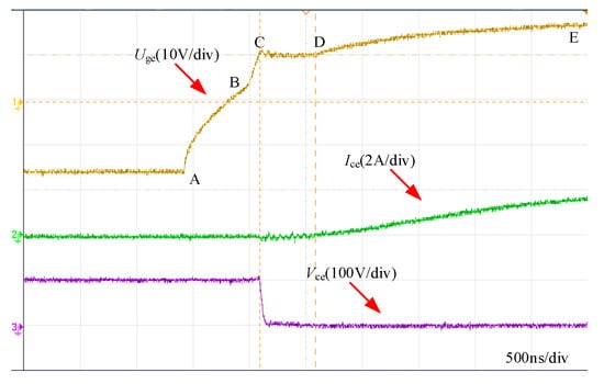
Figure 5.
Comparison chart of Uge, Ice, and Vce.
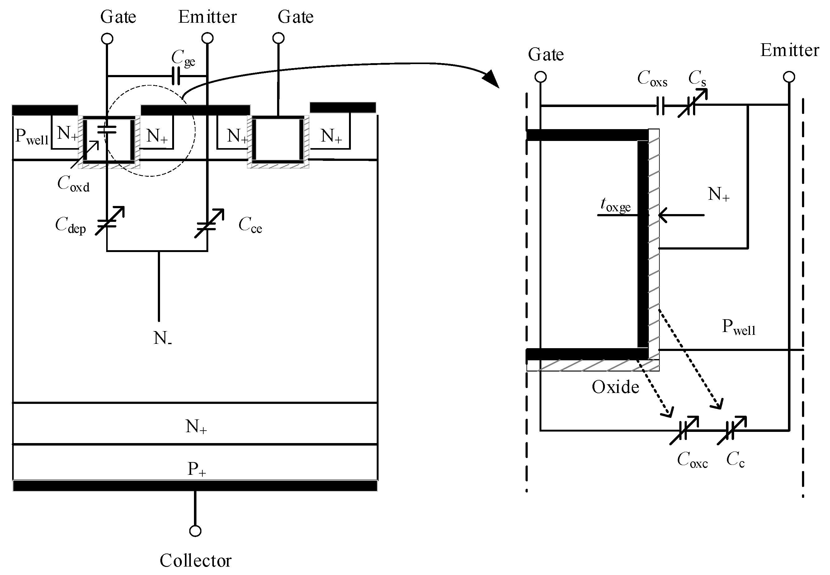
Thus, the Miller platform voltage Vm and the Miller platform duration tm are determined by the gate equivalent capacitance Cge and the feedback capacitance Cce (also called Miller capacitance). The effect of aging of the IGBT bond wire on the gate equivalent capacitance Cge and the feedback capacitance Cce were analyzed. A concrete diagram of the internal structure of the gate equivalent capacitor Cge and the feedback capacitor Cce of the IGBT is shown in Figure 6.
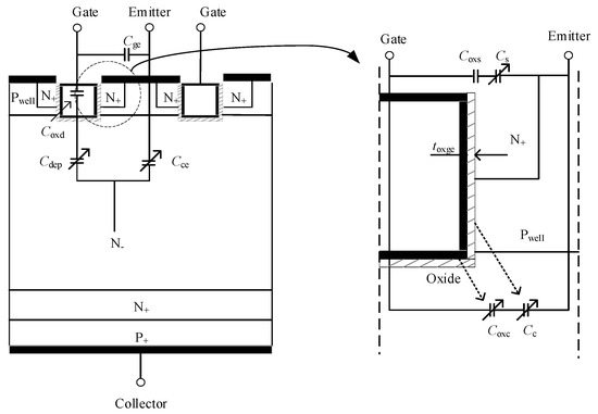
Figure 6.
IGBT internal equivalent capacitance diagram.
The gate equivalent capacitance Cge is usually composed of two parts. One part overlaps the gate polysilicon from the source N+ region, including Coxs and Cs, and another part overlaps the top surface of the gate polysilicon and the P well region, including Coxc and Cc. The specific mathematical expression of the gate equivalent capacitance is as follows:
with
where Ages and Agec represent the area of the gate polysilicon overlapping the source N+ region and the P-well region, respectively; toxge is the thickness of the oxide between them; and and are the dielectric constant and conductivity of the oxide, respectively. In the IGBT chip, the breakage caused by the aging of the bond wire leads to the decreasing of Ages and Agec, and this causes a decrease in Coxs and Coxc, even leading to a decrease in Cge.
The gate-collector capacitance, that is, the Miller capacitance Cce, is composed of a gate oxide capacitor Coxd and a depletion layer capacitor Cdep in series. The specific mathematical expression is as follows:
with
where Cox is the oxide capacitance per unit area; Aai is the area between the cells in the die; and W is the length of the oxide depletion region. As analyzed previously, the breakage caused by the bonding wire aging causes the Aai and W to decrease, which causes the gate oxide capacitance Coxd to decrease and the depletion layer capacitance Cdep to change, thereby causing the Miller capacitance Cce to change.
Based on the above analysis, we can find that the gate equivalent capacitance Cge and the Miller capacitance Cce change with the IGBT bond wire aging and breakage, therefore affecting the Miller platform voltage Vm and the Miller platform duration tm.
3. Accelerated Aging Experiment of IGBT Bonding Wire
3.1. Design Aging Experiment and Parameter Acquisition
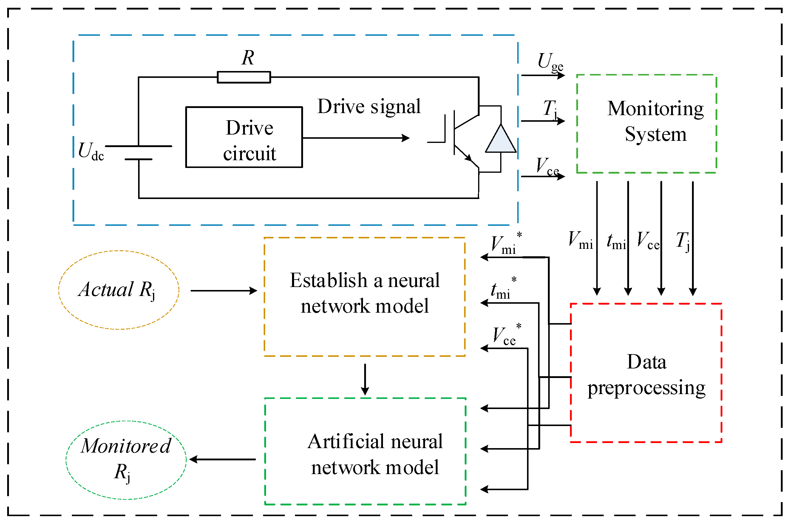
An IGBT aging test bench and monitoring system were built. The schematic diagram is shown in Figure 7. The main circuit consisted of a programmable DC power supply, a resistive load, and an IGBT. The drive circuit was composed of a function generator, an IGBT driver board, and a patch cord. The IGBT driver board could only drive the IGBT by setting the driving frequency in the function generator. The monitoring system consisted of a probe, a voltage sensor, a current sensor, a high-precision oscilloscope, and a host computer. The parameters used are shown in Table 1.
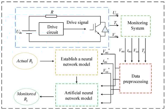
Figure 7.
Process diagram of monitoring and analysis.

Table 1.
Main circuit parameter.
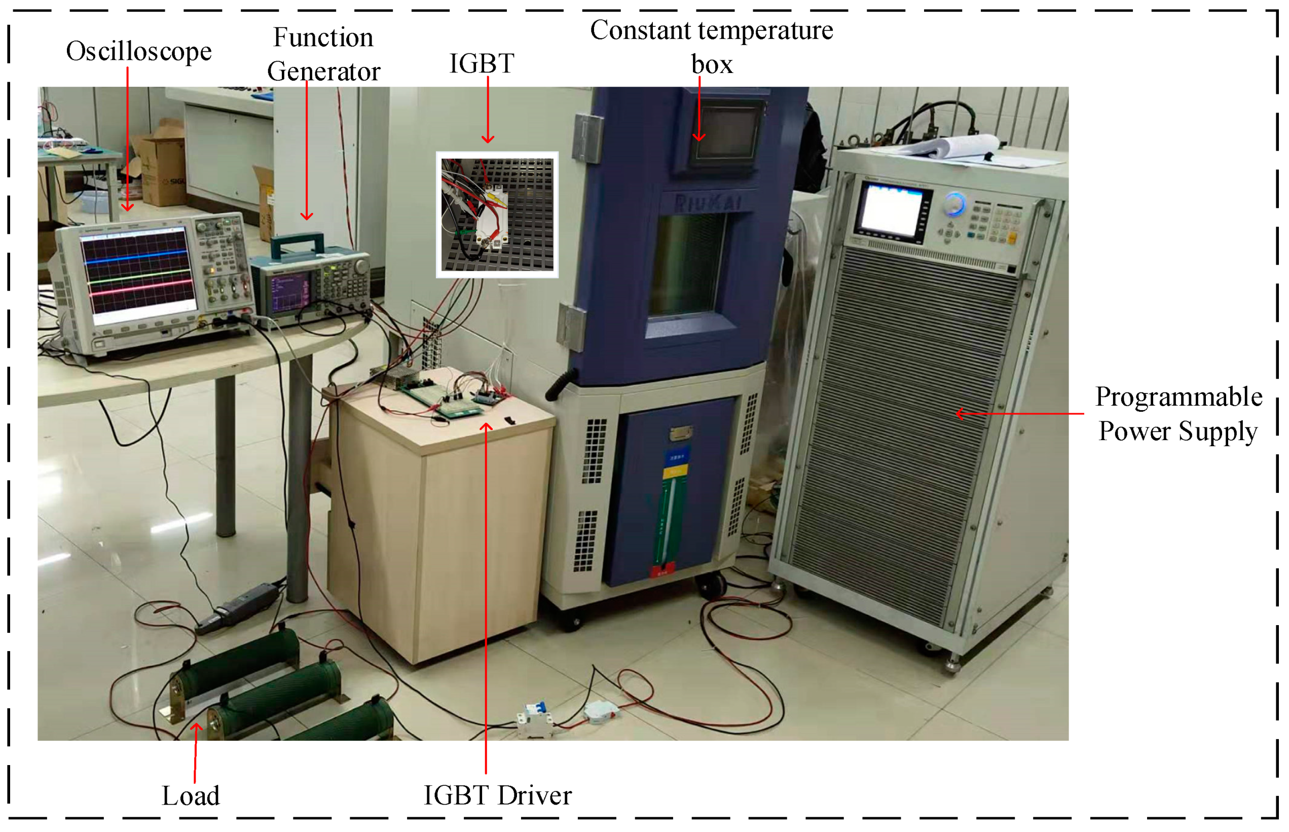
The aging failure in the IGBT operation by gradual damage to the IGBT bond wire (cutting the IGBT bond wire one by one) was simulated. Then, the electrical parameters under the online operation, which included the conduction voltage drop Vce, Miller platform voltage Vm, Miller platform duration tm, and temperature T, were separately recorded in different IGBT aging conditions. The physical diagram is shown in Figure 8.

Figure 8.
Physical diagram of the test system.
Nearly 90% of the simulation data for several IGBTs was used to establish the neural network relationship, while the rest was applied for verification of the method. As the actual waveform had voltage fluctuations, the actual voltage value and the average conduction voltage drop Vce and the Miller platform voltage Vm in one cycle was collected into the computer so as to get more reliable experimental data.
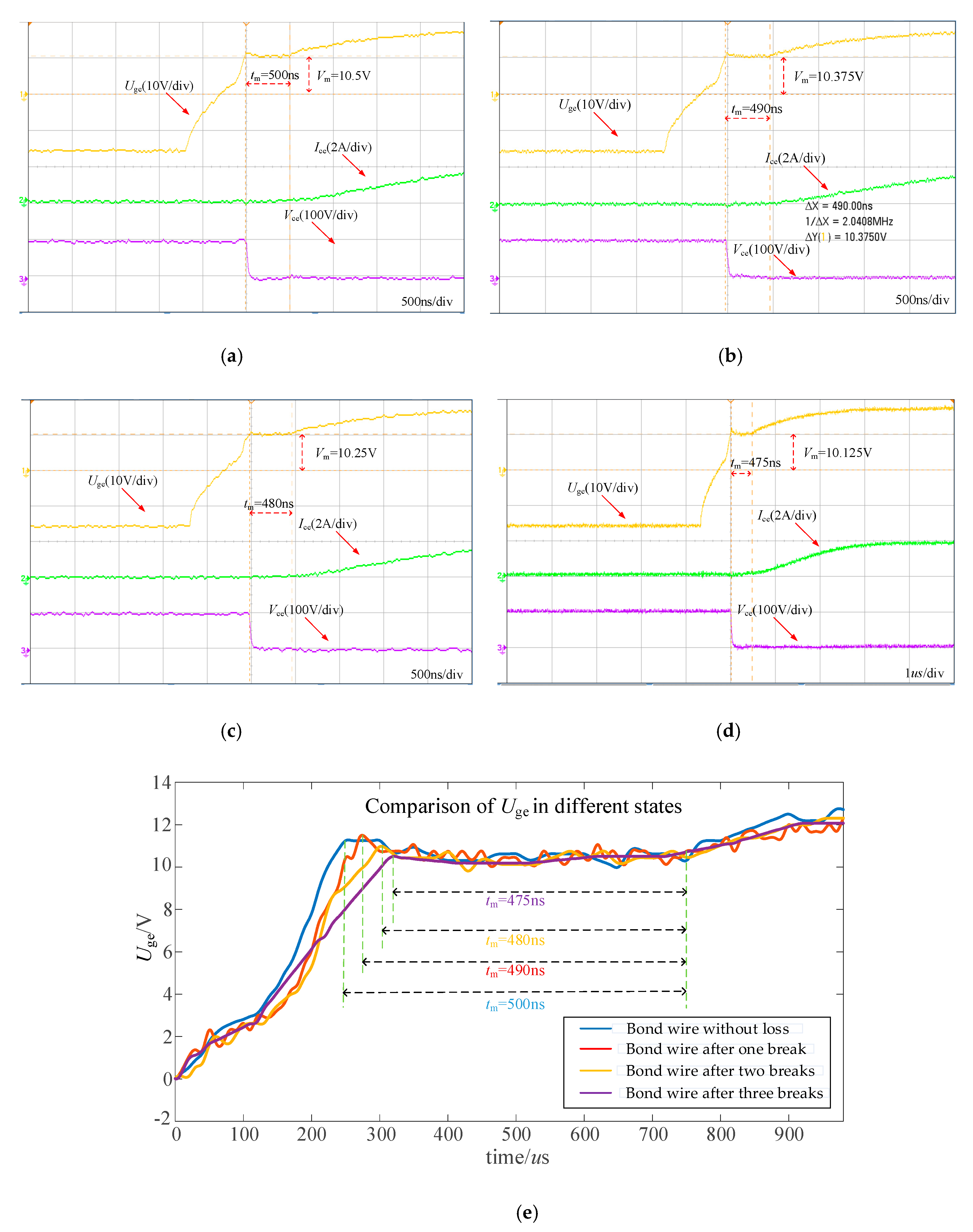
Figure 9 shows the effect of breakage of the bond wire, with each broken bond line indicating a 25% increase in bond aging. It can be seen the Miller plateau voltage gradually reduced, and the Miller platform duration also gradually reduced. This is because the bond wire breakage affected the change of the IGBT gate equivalent capacitance. The course changed as the process was affected. The specific structure of an IGBT is complicated, and it is difficult to quantitatively analyze the influence of bonding wire aging on Miller platform voltage value and Miller platform duration. Therefore, in this study, the neural network model was used for subsequent data processing to deal with this relationship.
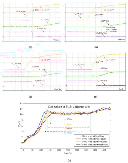
Figure 9.
Uge, Ice, and Vce waveforms with different IGBT bond line losses: (a) bond wire without loss; (b) bond wire after one break; (c) bond wire after two breaks; (d) bond wire after three breaks; (e) comparison of Uge with different IGBT bond line losses.
The average value of Vm in one cycle was taken as the actual value of the IGBT Miller platform voltage in the current state, thereby effectively reducing the measurement error. The IGBT turn-on voltage, the true value of the Miller platform voltage, and the Miller platform duration in the different states are shown in Table 2. It can also be seen from the table that the true value of the Miller platform voltage is the same as our analysis.
Table 2.
Actual value of Vm, Vce, and tm at different IGBT bond wire losses.
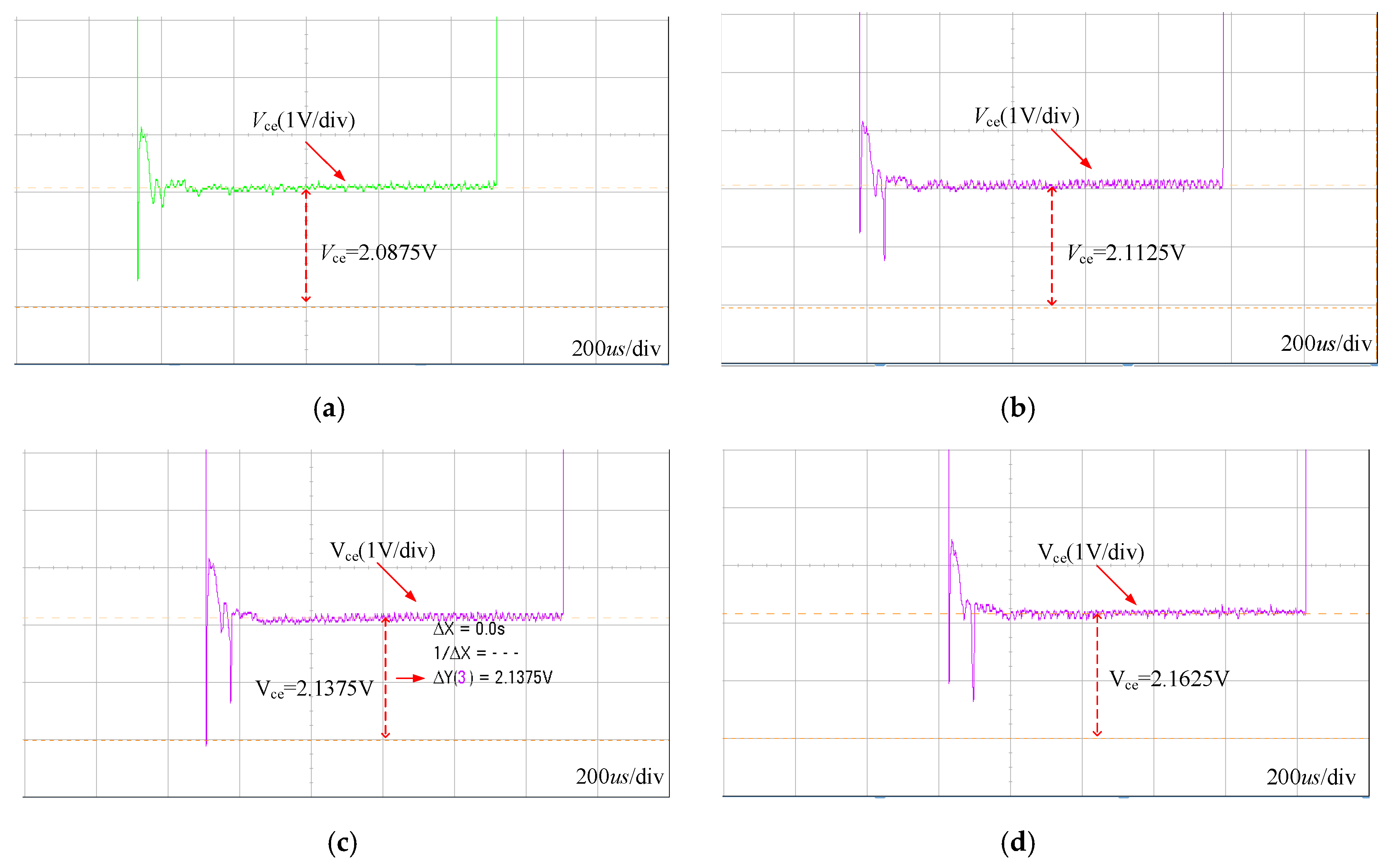
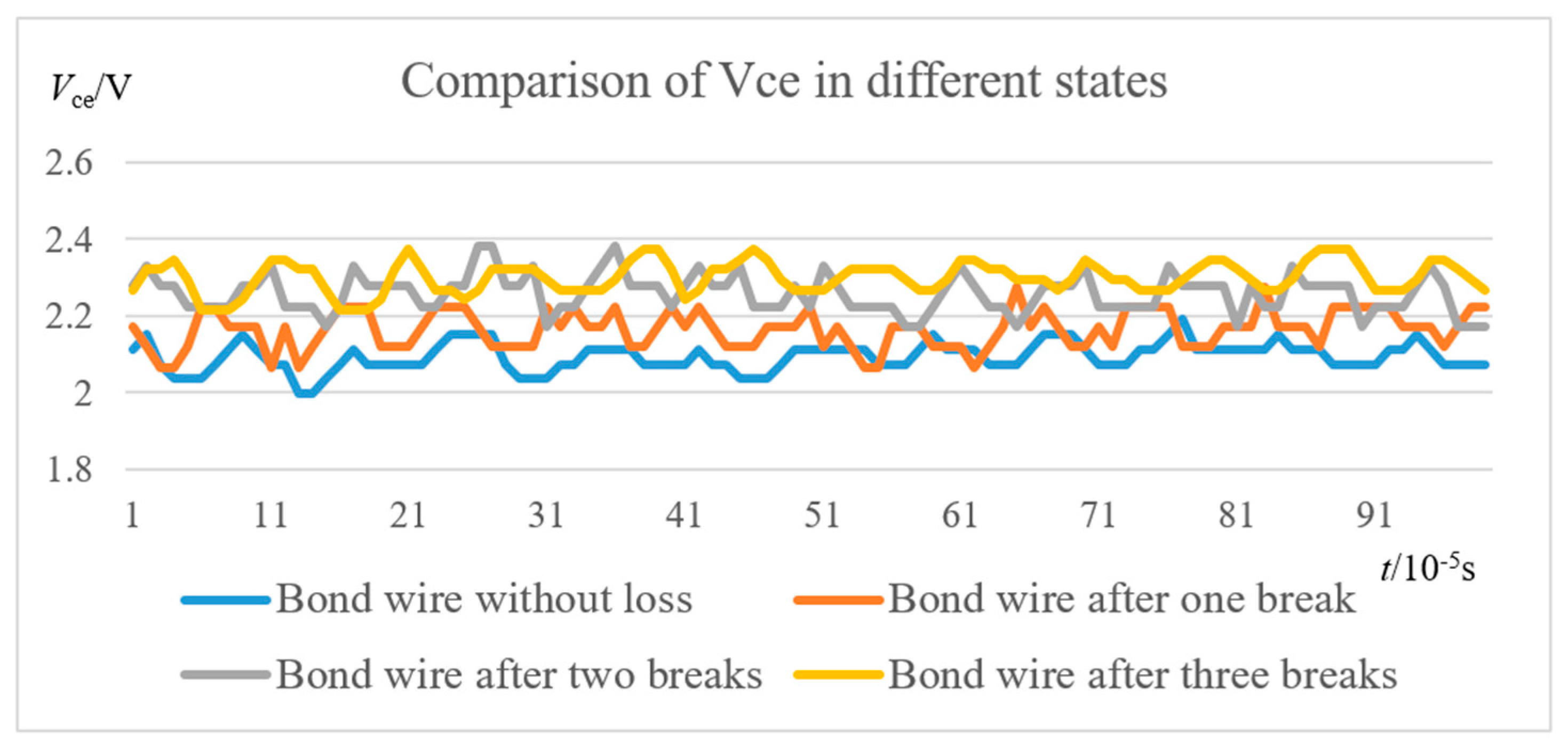
The above treatment was similarly performed on the turn-on voltage drop Vce. Figure 10 shows the change in Vce with the bond wire, while Figure 11 gives a comparison of Vce in different states. The actual value of Vce in one cycle was averaged as the true value of the IGBT turn-on voltage in the current state. It can also be seen from Table 2 that the true value of the turn-on voltage is the same as our analysis.
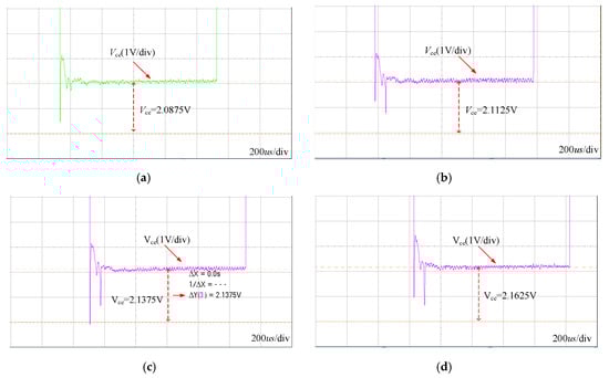
Figure 10.
Waveform of Vce at different IGBT bond wire losses: (a) bond wire without loss; (b) bond wire after one break; (c) bond wire after two breaks; (d) bond wire after three breaks.
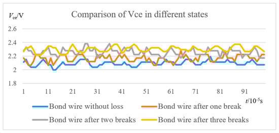
Figure 11.
Comparison of Vce in different states.
3.2. Junction Temperature Conversion Experiment
As the IGBT operates under different working conditions, the internal junction temperature of the IGBT is different, and the change of the temperature causes the internal resistance of the IGBT to change. Therefore, the on-voltage drop Vce, the Miller platform voltage Vm, and the Miller platform duration tm of the IGBT vary depending on the junction temperature, which affects predictions. In order to avoid this effect, the IGBT was placed in an incubator to establish the relationship between the junction temperature of the IGBT at different temperatures and the on-state voltage drop Vce, the Miller platform voltage Vm, and the Miller platform duration tm. When the data was processed, the Vce, Vm, and tm at the current temperature were corrected, and the data obtained at different temperatures were equivalent to the data monitored at the same temperature, thus avoiding the influence of the junction temperature fluctuation on the experimental results.
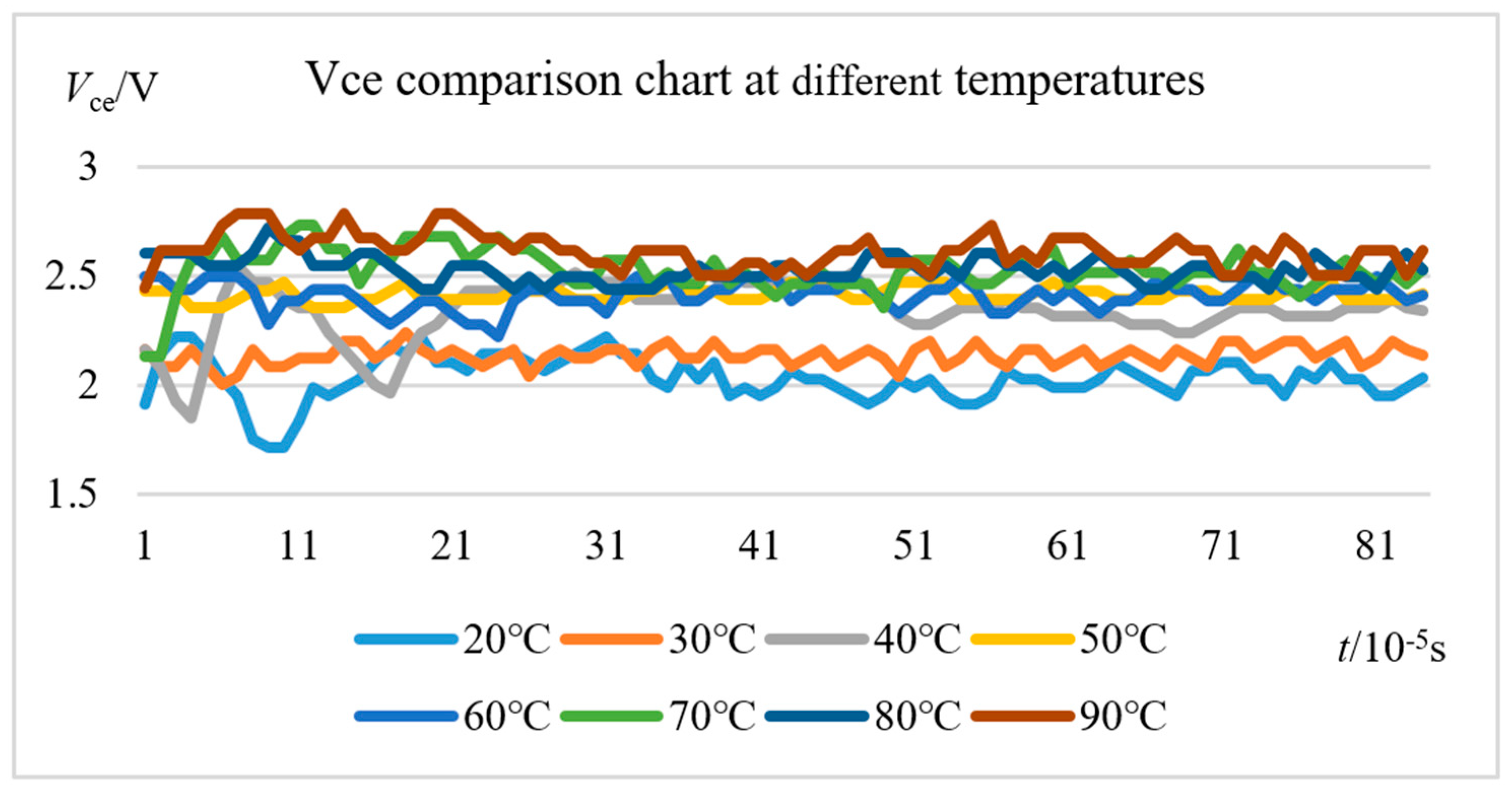
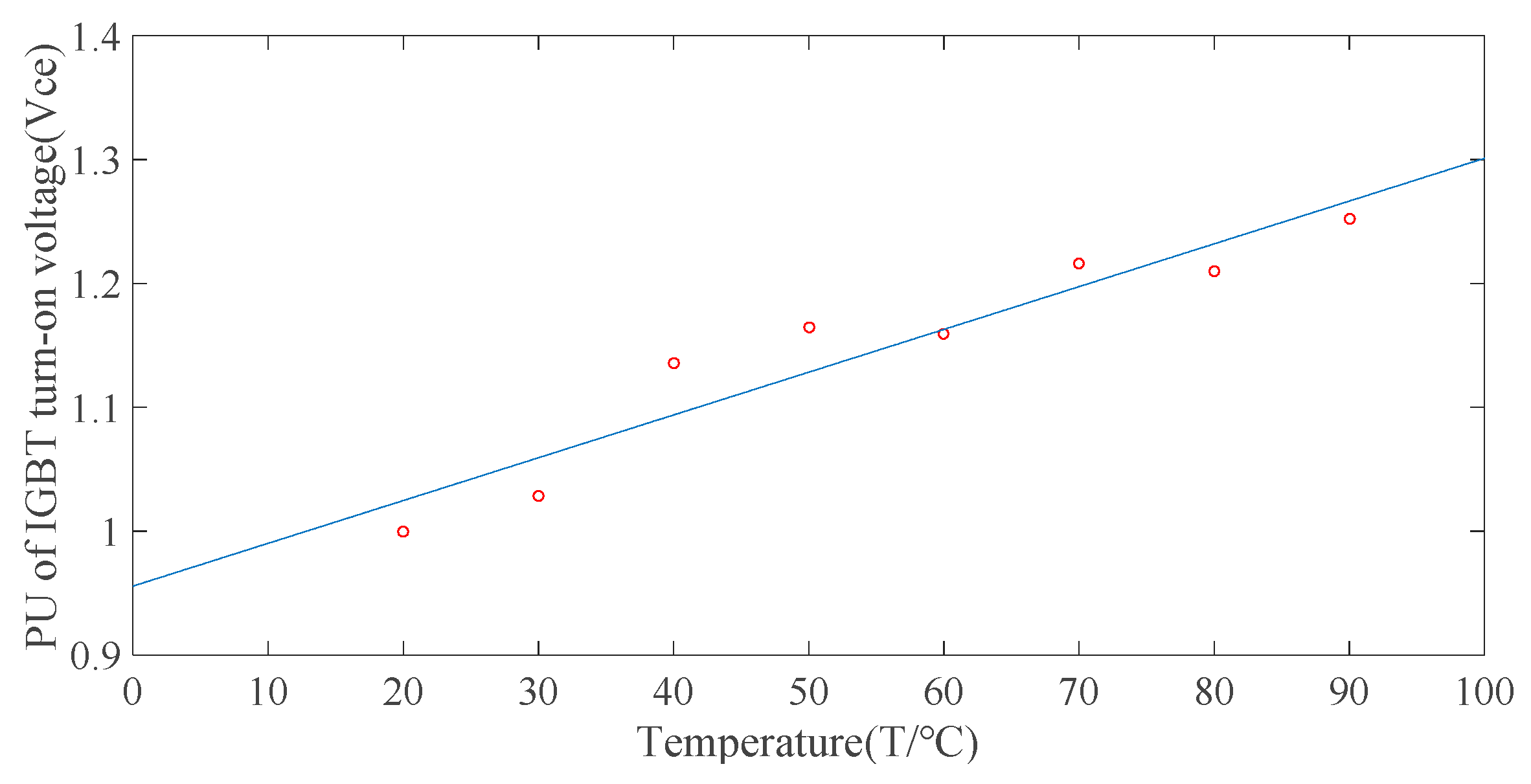
The change in the IGBT turn-on voltage drop Vce in the same state at different temperatures was measured, as shown in Figure 12. It can be seen that there was a significant change in the conduction voltage drop Vce at different temperatures. In addition, it is obvious that, as the temperature rose, the IGBT turn-on voltage drop Vce gradually increased. However, because there was a certain voltage fluctuation when the IGBT was turned on, preliminary processing was performed on the Vce before fitting the relationship between the conduction voltage drop Vce and the IGBT junction temperature. The actual data was then collected into the computer. The Vce of the on-period was averaged as the actual value of the IGBT turn-on voltage drop at the current temperature. The results are shown in Table 3.
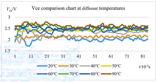
Figure 12.
Comparison of Vce at different temperatures.
Table 3.
Actual value of Vce at different temperatures.
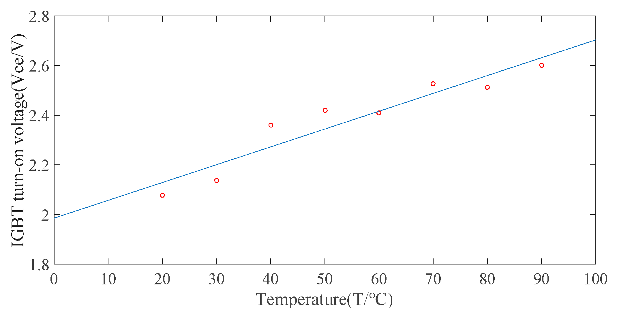
It can be clearly seen that, as the temperature rose, the IGBT conduction voltage drop also increased. We made a function fit of the junction temperature and the tube pressure drop. Figure 13 is a fitted graph, and the fitting results were as follows:
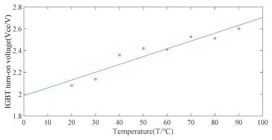
Figure 13.
A function fitting diagram of Vce and T.
Because IGBTs have different conduction voltages Vce at the same temperature, the fitting data wad made usable for different IGBT monitoring by standardizing Vce at 20 °C at different temperatures. The relationship between the conduction voltage drop and the temperature after the standardization at different temperatures was obtained. Table 4 is the data of the conduction voltage drop Vce after the standardization, and Figure 14 is the fitting map after the standardization. The fitting results were obtained as follows:
Table 4.
Comparison of Vce at different temperatures.
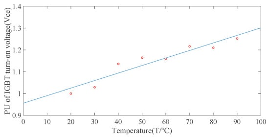
Figure 14.
A function fitting diagram of Vce* and T.
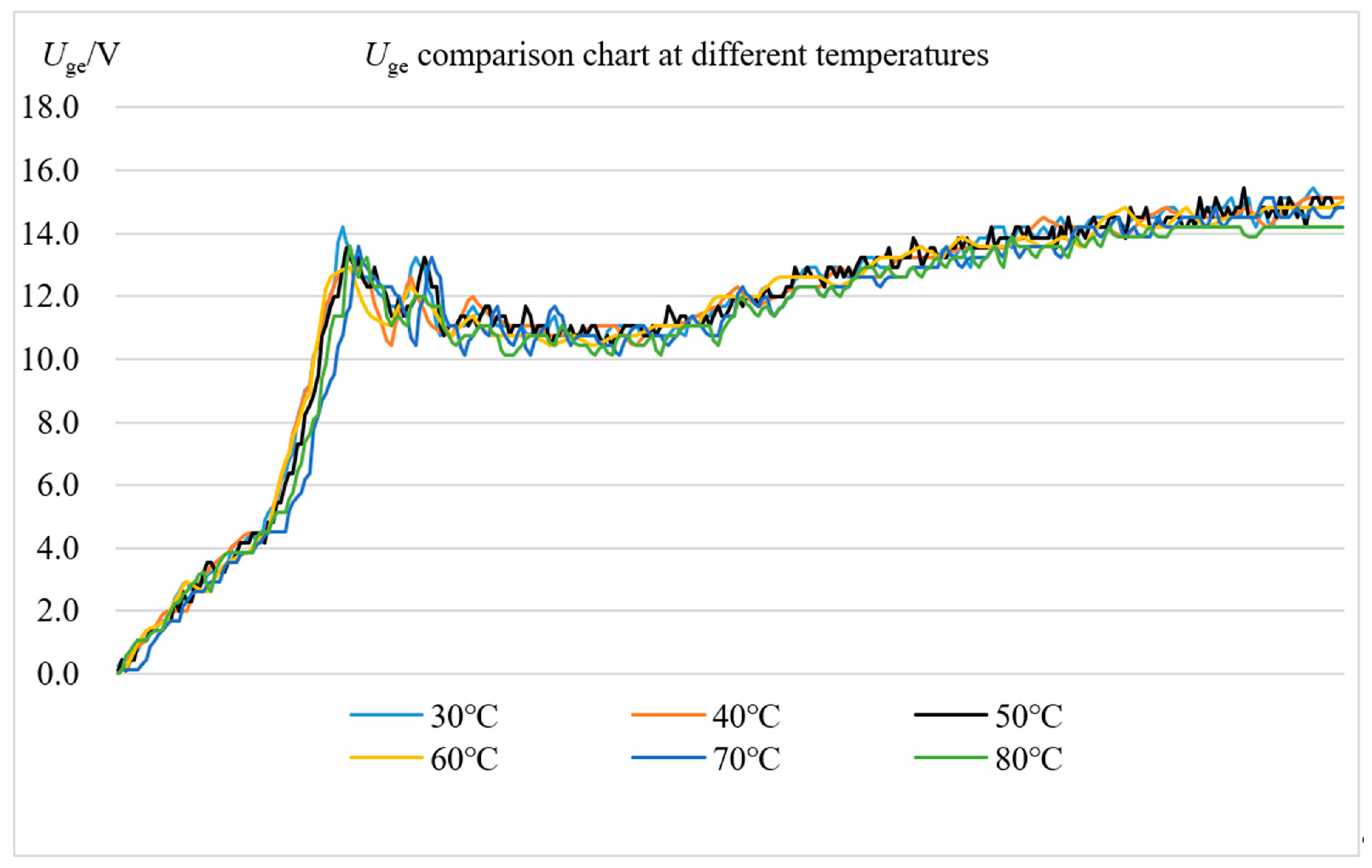
Table 4 shows the correspondence between Vce* and T at a partial temperature. Meanwhile, the change of gate voltage Uge at different temperatures is illustrated in Figure 15. It is obvious that Uge was basically unchanged with the IGBT junction temperature, which means that Uge was basically unaffected by the change in IGBT junction temperature. The literature [20,21] also shows that the Miller platform voltage is not affected by the IGBT junction temperature. Considering the fact that Vm is not affected by the IGBT temperature, taking the average value of Vm at different temperatures as the actual value of Vm, as shown in Table 5, it is clear that Uge has no relationship with junction temperature.
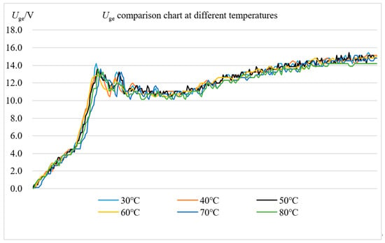
Figure 15.
Comparison of Uge at different temperatures.
Table 5.
Table of actual values of Vm as a function of temperature.
4. The Method of Monitoring IGBT Bond Wire Aging
4.1. Artificial Neural Networks
With the increasing speed of the CPU, more and more neural network structures are used to solve the mapping relationship between parameters. In this study, through theoretical analysis and experimental conclusions, it was found that there is a relationship between the saturation conduction voltage drop Vce of the IGBT, the Miller platform voltage Vm, the Miller platform time tm, and the bond line equivalent resistance Rj. As mentioned above, the breakage of the bonding wire affects the change of the equivalent capacitance of the IGBT gate, which causes the conduction process to be affected and changed. This law of variation is nonlinear, and it is difficult to quantitatively analyze the influence of bond line aging on Miller platform voltage value and Miller platform duration. It is meaningful to use the ANN structure to establish the corresponding relationship. Therefore, there is a need to fully analyze the specific relationship between the gate voltage Uge and the degree of bond line loss when IGBT is turned on.
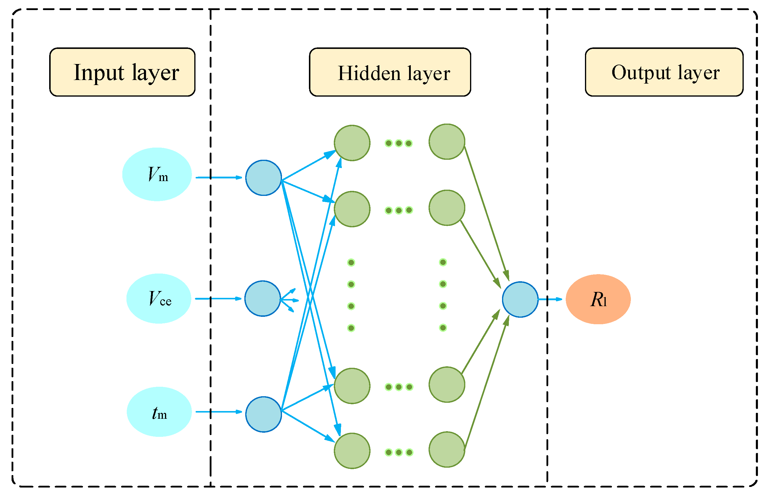
As shown in Figure 16, by substituting the test result data after the junction temperature correction and the standardization experiment, the saturation conduction voltage drop Vce of the IGBT, the Miller platform voltage Vm, and the Miller platform time tm were set as the input layer. The bond wire loss rate Rloss was set to the output layer, and the ANN correspondence was established by setting a reasonable activation function f(x) in the neural network toolbox. After establishing the neural network structure, the current IGBT bond wire loss rate could be calculated by inputting the result obtained from online monitoring of the IGBT.
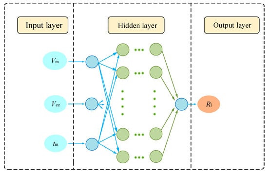
Figure 16.
Structural diagram of artificial neural network (ANN).
4.2. Establishment of Multivariate Parameters and Bond Line Aging
Due to the small gap in the actual production of IGBTs, even if the internal equivalent electrical parameters of the same type of IGBT have small gaps, it is necessary to standardize the on-voltage drop Vce, Miller platform voltage Vm, and Miller platform duration tm in order to make the neural network widely usable in the monitoring of similar types of IGBTs. The standard value of the standardization was taken as the value when the bonding wire had no loss. Then, using the relationship between the conduction voltage drop and the temperature established in the study, the conduction voltage drop Vce was corrected at the current junction temperature and uniformly converted to a value at a junction temperature of 20 °C. Four IGBT bond wires were used in the study. Using the bond wire loss rate Rloss to quantify the current IGBT bond wire loss degree, the loss rate Rloss was 0% when the bond wire was intact, 25% when the bond wire broke once, 50% when the bond wire broke twice, and 75% when the bond wire broke three times. Table 6 shows the data before the standardization, and Table 7 shows the data after the standardization. Table 8 gives a comparison of the data before and after the junction temperature conversion.
Table 6.
Data before standardization.
Table 7.
Data after standardization.
Table 8.
Comparison of the data before and after the junction temperature conversion.
Finally, the processed training set data was input to the ANN, and iterative training was performed to establish a corresponding neural network. It can be seen from the results that the accuracy of the neural network correspondence can be verified using a training set.
4.3. Verification of Results
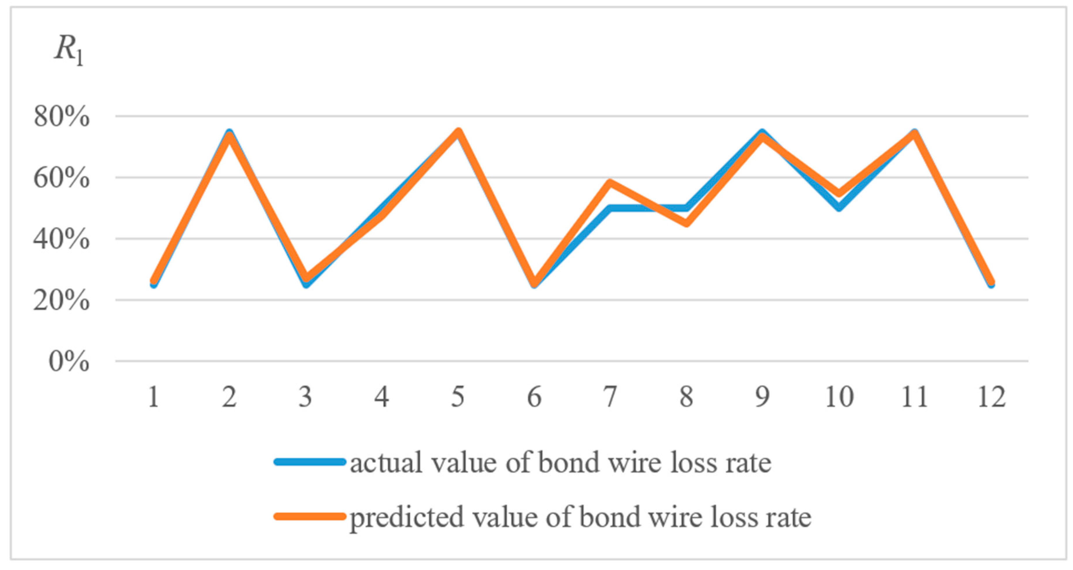
In order to verify the effectiveness of the proposed method after establishing the corresponding neural network, the processed verification data was input into the neural network, and the monitored value results and the actual results were output, as shown in Table 9 and Figure 17. From the results, it can be seen that the monitored value results are very close to the theoretical value results, which indicates that the proposed method in this paper is effective.
Table 9.
Comparison of monitored and actual values.
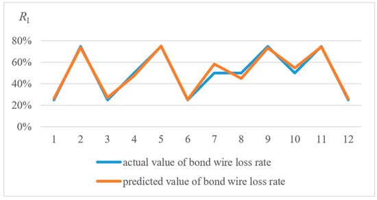
Figure 17.
Diagram comparing the monitored and actual values.
4.4. Comparison between Univariate Monitoring and Multivariate Monitoring
A single variable was used to evaluate the aging of IGBT bond wires, and the corresponding results were compared to that of the multivariate monitoring method.
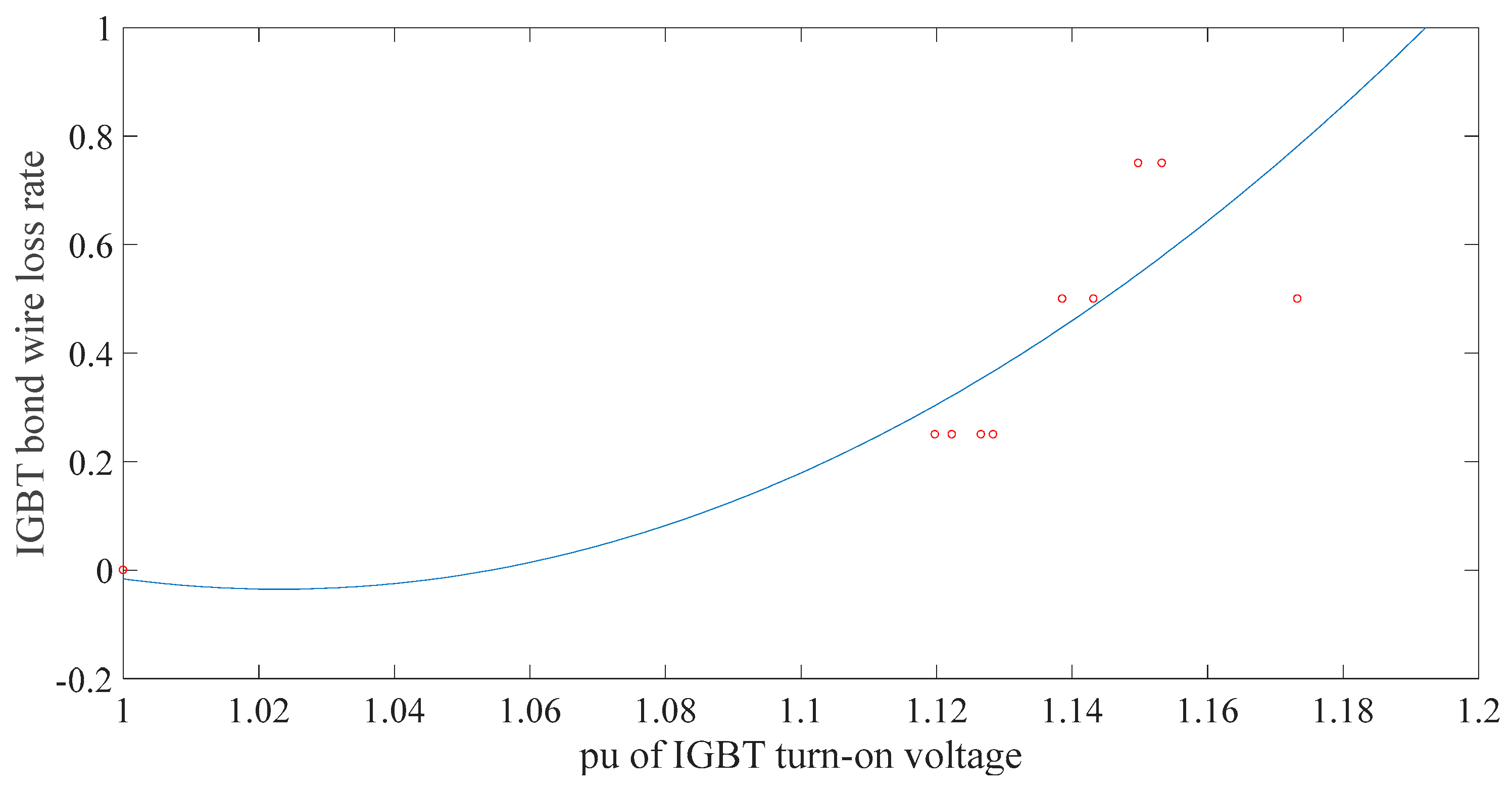
When using the univariate Vce to evaluate the aging degree of the IGBT bond wire, the function fitting method was directly adopted, and Figure 18 shows the corresponding result. The fitting result is as follows:
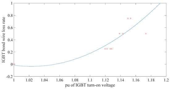
Figure 18.
Fitted function between the univariate Vce* and Rloss.
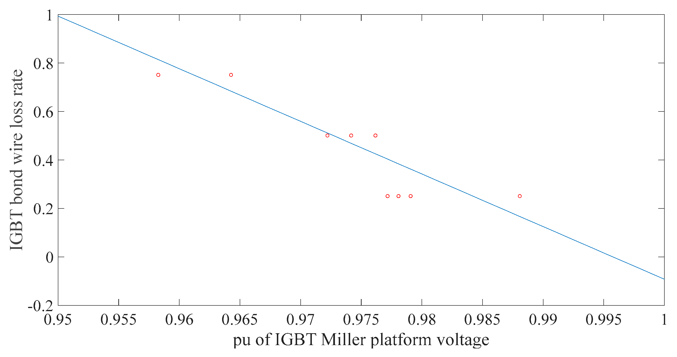
Similarly, the fitted functions between the univariate Vm and the IGBT bond wire loss rate Rloss as well as that between tm and Rloss were adopted, and the results are presented in Figure 19 and Figure 20, respectively. The fitting results are as follows:
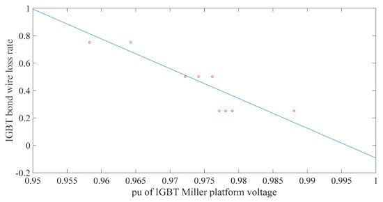
Figure 19.
Fitted function between the univariate Vm* and Rloss.
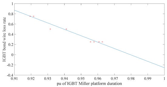
Figure 20.
Fitted function between the univariate tm* and Rloss.
Implementing the function of Equations (11)–(13), the estimated value of the IGBT bond wire loss rate were calculated and accordingly compared to the actual value. A comparison between the estimated value and the actual value in terms of the IGBT bond wire loss rate is given in Table 10. Additionally, it can be observed from Table 10, Table 11 and Table 12 that the average monitoring errors were Δe1 = 17.24%, Δe2 = 7.72%, and Δe3 = 11.52%, respectively.
Table 10.
Comparison of the estimated and actual values (using the univariate Vce).
Table 11.
Comparison of monitored and actual values(using the univariate Vm).
Table 12.
Comparison of monitored and actual values (using the univariate tm).
The average error Δe was 2.47% when multivariable was used to evaluate the aging degree of IGBT bond wires, which is significantly lower than that of the univariate evaluation, indicating that multivariate monitoring was more accurate.
5. Conclusions
On the basis of analyzing the aging of IGBT bond wire in relation to on-voltage (Vce), Miller plateau voltage (Vm), and Miller platform duration (tm), an online monitoring method with ANN is proposed in this paper for evaluating the degradation of IGBT bond wires. Before ANN was constructed with Vce, Vm, tm, and IGBT bond wire loss rate, Vce, Vm, and tm were subjected to standardization and junction temperature correction so that the method could be suitable for online monitoring of bond wire aging for different types of IGBTs. The main conclusions of this study are as follows: (1) As the IGBT bond wire aged and broke (the bond wire loss rate increased), its turn-on voltage increased, the Miller plateau voltage decreased, and the Miller platform duration decreased. (2) The monitored value of the IGBT bond wire loss rate obtained by the proposed method was close to the actual value, and the average error was 2.47%, which indicates that the method is feasible and effective. The reliability of an electronic device can be improved by avoiding failure of the entire device due to IGBT failure. This requires pre-identification of the aging degree of IGBT bond wire. In this regard, the method presented in this paper allows replacement of the IGBT module before module failure. When using this method in future works, if the actual aging of the IGBT bond wire is obtained, the result will be more reliable and more realistic. At the same time, monitoring the aging of other locations of the IGBT module is also required. In addition, considering the turn-off voltage and current to evaluate the aging degree of IGBT bond wire is open to further research.
Author Contributions
Writing—original draft preparation, Z.H. and F.Y.; methodology, Z.H. and X.G.; writing—review and editing, D.X. and X.G.; supervision, X.G.; funding acquisition, X.G.; software, B.Y. and J.D.; validation Z.H. and Y.Z.; formal analysis, Z.H.; conceptualization, Z.H. and X.G.; data curation, Z.H.
Funding
This research was funded by National Natural Science Foundation of China: 51677156, National Natural Science Foundation of China: 61733015.
Conflicts of Interest
The authors declare no conflict of interest.
References
- Stockmeier, T. From Packaging to “Un”-Packaging-Trends in Power Semiconductor Modules. In Proceedings of the 20th International Symposium on Power Semiconductor Devices and ICs, Orlando, FL, USA, 18–22 May 2008. [Google Scholar]
- Hensler, A.; Lutz, J.; Thoben, M.; Zachariae, J. Power cycling tests at high temperatures with IGBT power modules for hybrid electrical vehicle applications. In Proceedings of the 3rd Electronics System Integration Technology Conference ESTC, IEEE, Berlin, Germany, 13–16 September 2010; pp. 1–6. [Google Scholar]
- Ciappa, M. Selected failure mechanisms of modern power modules. Microelectron. Reliab. 2002, 42, 653–667. [Google Scholar] [CrossRef]
- Kostandyan, E.E.; John, D.S. Reliability assessment of solder joints in power electronic modules by crack damage model for wind turbine applications. Energies 2011, 12, 2236–2248. [Google Scholar] [CrossRef]
- Wang, H.; Ge, X.; Liu, Y. An Active Damping Stabilization Scheme for the Suppression of the DC-Link Oscillation in Metro Traction Drive System. IEEE Trans. 2018, 54, 5113–5123. [Google Scholar] [CrossRef]
- Ciappa, M.; Wolfgang, F. Lifetime prediction of IGBT modules for traction applications. In Proceedings of the 38th Annual 2000 IEEE International Reliability Physics Symposium, San Jose, CA, USA, 10–13 April 2000. [Google Scholar]
- Kovacevic, I.F.; Uwe, D.; Johann, W.K. New physical model for lifetime estimation of power modules. In Proceedings of the 2010 International Power Electronics Conference (ECCE-Asia), Sapporo, Japan, 21–24 June 2010. [Google Scholar]
- Bayerer, R.; Herrmann, T.; Licht, T.; Lutz, J.; Feller, M. Model for power cycling lifetime of IGBT modules-various factors influencing lifetime. In Proceedings of the 5th International Conference on Integrated Power Electronics Systems, Nuremberg, Germany, 11–13 July 2008. [Google Scholar]
- Zhou, L.; Shengqi, Z.; Mingwei, X. Investigation of gate voltage oscillations in an IGBT module after partial bond wires lift-off. Microelectron. Reliab. 2013, 53, 282–287. [Google Scholar] [CrossRef]
- Sutrisno, E. Fault Detection and Prognostics of Insulated Gate Bipolar Transistor (Igbt) Using A K-Nearest Neighbor Classification Algorithm. Ph.D. Thesis, University of Maryland, College Park, MD, USA, 2013. [Google Scholar]
- Kong, Q.; Du, M.; Ouyang, Z.; Wei, K.; Hurley, W.G. A method to monitor IGBT module bond wire failure using on-state voltage separation strategy. Energies 2019, 12, 1791. [Google Scholar] [CrossRef]
- Brown, D.W.; Abbas, M.; Ginart, A.; Ali, I.N.; Kalgren, P.W.; Vachtsevanos, G.J. Turn-off time as an early indicator of insulated gate bipolar transistor latch-up. IEEE Trans. Power Electron. 2011, 27, 479–489. [Google Scholar] [CrossRef]
- Ji, B.; Pickert, V.; Cao, W.; Zahawi, B. In situ diagnostics and prognostics of wire bonding faults in IGBT modules for electric vehicle drives. IEEE Trans. Power Electron. 2013, 28, 5568–5577. [Google Scholar] [CrossRef]
- Patil, N.; Celaya, J.; Das, D.; Goebel, K.; Pecht, M. Precursor parameter identification for insulated gate bipolar transistor (IGBT) prognostics. IEEE Trans. Reliab. 2009, 58, 271–276. [Google Scholar] [CrossRef]
- Smet, V.; Forest, F.; Huselstein, J.J.; Richardeau, F.; Khatir, Z.; Lefebvre, S.; Berkani, M. Ageing and failure modes of IGBT modules in high-temperature power cycling. IEEE Trans. Ind. Electron. 2009, 58, 4931–4941. [Google Scholar] [CrossRef]
- Pedersen, K.B.; Kristensen, P.K.; Popok, V.; Pedersen, K. Degradation assessment in IGBT modules using four-point probing approach. IEEE Trans. Power Electron. 2014, 30, 2405–2412. [Google Scholar] [CrossRef]
- Li, K.; Tian, G.Y.; Cheng, L.; Yin, A.; Cao, W.; Crichton, S. State detection of bond wires in IGBT modules using eddy current pulsed thermography. IEEE Trans. Power Electron. 2013, 29, 5000–5009. [Google Scholar] [CrossRef]
- Busca, C. Modeling lifetime of high power IGBTs in wind power applications-An overview. In Proceedings of the 2011 IEEE International Symposium on Industrial Electronics, Gdansk, Poland, 27–30 June 2011. [Google Scholar]
- Tseng, K.C.; Chen, J.Z.; Lin, J.T.; Huang, C.C.; Yen, T.H. High step-up interleaved forward-flyback boost converter with three-winding coupled inductors. IEEE Trans. Power Electron. 2014, 30, 4696–4703. [Google Scholar] [CrossRef]
- Peng, Y.; Sun, P.; Zhou, L.; Du, X.; Cai, J. A temperature-independent method for monitoring the degradation of bond wires in IGBT modules based on transfer characteristics. In Proceedings of the 2017 IEEE Applied Power Electronics Conference and Exposition (APEC), Tampa, FL, USA, 26–30 March 2017. [Google Scholar]
- Sun, P.; Gong, C.; Du, X.; Peng, Y.; Wang, B.; Zhou, L. Condition monitoring IGBT module bond wires fatigue using short-circuit current identification. IEEE Trans. Power Electron. 2016, 35, 3777–3786. [Google Scholar] [CrossRef]

© 2019 by the authors. Licensee MDPI, Basel, Switzerland. This article is an open access article distributed under the terms and conditions of the Creative Commons Attribution (CC BY) license (http://creativecommons.org/licenses/by/4.0/).