Abstract
The paper deals with the problem of modelling and analyzing the dynamic properties of a Junction Field Effect Transistor (JFET) made of silicon carbide. An examination of the usefulness of the built-in JFET Simulation Program with Integrated Circuit Emphasis (SPICE) model was performed. A modified model of silicon carbide JFET was proposed to increase modelling accuracy. An evaluation of the accuracy of the modified model was performed by comparison of the measured and calculated capacitance–voltage characteristics as well as the switching characteristics of JFETs.
1. Introduction
Nowadays, the dynamic development of high-power electronic systems requires modern electronic components and devices that are characterized by improved electrical and thermal properties [1,2,3,4]. A new generation of junction field-effect transistors made of silicon carbide (SiC-JFETs) has appeared on the market as a result of technological progress in the construction of semiconductor devices [1,3,5]. SiC-JFETs are characterized by better static properties, i.e., higher values of absolute maximum ratings of operating currents, terminal voltages and dissipated power as well as dynamic properties related to short switching times [5,6,7].
The dynamic properties of a JFET depend on, among others, the values of diffusion and junction capacitances of the internal gate-source and gate-drain p–n junctions of the transistor [8,9,10]. Both capacitances are functions of the terminal voltage applied and play an important role in the forward and the reverse polarization of the device. On the other hand, the dynamic properties of JFETs are characterized by parasitic capacitances resulting from the non-zero size of the transistor structure [8,9,10,11].
In the design and analysis of power electronic devices and circuits, an appropriate computer tool containing reliable models of semiconductor devices is needed. One of the most popular computer programs used for the modeling and analysis of electronic devices and circuits is the Simulation Program with Integrated Circuit Emphasis (SPICE) [12]. SPICE contains a large number of passive and active device models. The accuracy of SPICE models for various semiconductor devices, such as MOSFET, BJT, SJT and IGBT transistors, has already been studied [13,14,15,16,17,18].
In the case of JFET characteristics modelling, a Shichman–Hodges (S–H) model is used [12]. Recently, a successful attempt at modeling the static characteristics and parameters of SiC-JFETs using the S–H model have been reported [19,20]. On the other hand, selected aspects of modelling dynamic characteristics of JFETs were presented in [8,9,10,21,22,23,24].
The paper deals with the problem of modelling capacitance–voltage (C–V) as well as switching characteristics of SiC-JFETs. Appropriate modifications of the Shichman–Hodges model were proposed in order to improving its accuracy. The modified model was experimentally verified by comparison of the measured and calculated C–V characteristics of the transistor. Moreover, the results of measurements and calculations of the switching characteristics of the transistor were compared.
2. The Shichman–Hodges Model Form
A network form of the built-in in SPICE Shichman–Hodges model of JFET is presented in Figure 1 [12].
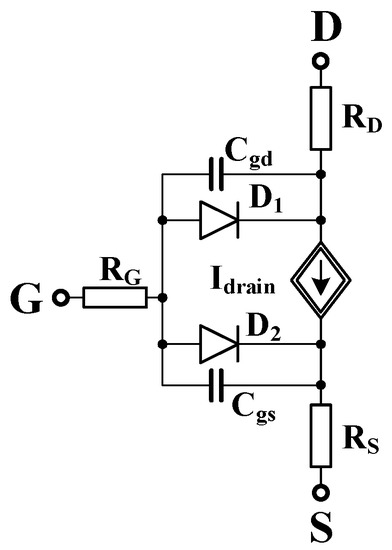
Figure 1.
Network form of the Shichman–Hodges (S–H) model of the junction field-effect transistor (JFET) in Simulation Program with Integrated Circuit Emphasis (SPICE).
The main element of the presented model is the controlled source Idrain modeling static drain current of the transistor for three operational regions, according to the equations [12,19]:
- in the cut-off region (for VGS−VTO(T) < 0):
- in the linear region (for VDS ≤ VGS−VTO(T)):
- in the saturation region (for 0 < VGS−VTO(T) < VDS):where: VGS—gate-source voltage, VDS—drain-source voltage, LAMBDA—channel-length modulation coefficient, BETA(T)—temperature dependence of transconductance coefficient, VTO(T)—temperature dependence of the threshold voltage.
Resistors RG, RD and RS (Figure 1) represent series resistances of the gate, the drain and the source of the transistor. Diodes D1 and D2 describe currents of the gate–source and the gate–drain p–n junctions, respectively. An extended description of the static S–H model is given for instance in [20] or is available in the SPICE user manual [12].
Capacitors Cgs and Cgd (Figure 1) represent nonlinear junction capacitances of p–n junctions, according to equations [3,8]:
- for Vgs ≤ FC·PB
- for Vgs > FC·PB
- for Vgd ≤ FC·PB
- for Vgd > FC·PBwhere: FC—forward-bias depletion capacitance coefficient, PB—gate p–n potential, CGS, CGD—zero-bias gate–source and gate–drain junction capacitances, M—gate p–n grading coefficient.
3. Results of Simulations of the Shichman–Hodges Model
A normally-OFF trench silicon carbide power Junction Field-Effect Transistor of absolute maximum drain-source voltage equal to 1700 V (SJEP170R550) fabricated by SemiSouth [25] was chosen for investigations. Measurements of capacitance characteristics were performed using the measuring source Keithley 2602. The JFET model parameters were calculated using an estimation method described in [26]. Values of static model parameters for the considered transistor are: BETA = 2.308 A/V2, LAMBDA = 0.0538 V−1, IS = 1·10−16 A, ISR = 4.51·10−9 A, M = 0.0164, N = 3.152, NR = 9.62, PB = 6.832 V, RD = 0.4113 Ω, RS = 0.0346 Ω, VTO = 0.8576 V, XTI = 2, BETATCE =−0.0994 %/°C, VTOTC = 6.1494·10−4 V/°C.
In addition, values of parameters describing the capacitance of the considered transistor model are as follows: CGD = 2.57·10−10 F, CGS = 1.34·10−10 F, FC = 0.5.
Results of measurements and calculations of C–V characteristics using S–H model are presented in Figure 2. Points and solid lines in Figure 2 denote the results of measurements and calculations, respectively.
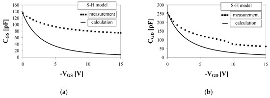
Figure 2.
(a,b) Measured and calculated (S–H model) capacitance–voltage characteristics of the SiC JFET.
As seen, for small VGS and VGD bias voltages of around 1 V a good agreement between the simulation and measurement results can be observed. However, quantitative and qualitative discrepancies reaching even one order of magnitude are observed in the case of CGS(V) and CGD(V) characteristics (Figure 2a,b) for voltages greater than 1 V.
The manufacturers of the JFET transistors present in datasheets [25] the characteristics of capacitances Ciss, Coss and Crss as a function of specified terminal voltages. These capacitances constitute an appropriate combination of transistor junction capacitances. Capacitances Ciss, Coss and Crss are expressed with the following formulas [10]:
where Cgs—gate–source capacitance, Cgd—gate–drain capacitance, and Cds—drain–source capacitance.
Calculations of C–V characteristics of the transistor can be realized using specialized SPICE simulation circuits [10]. The network forms of Ciss and Crss measurement fixtures are presented in Figure 3 and Figure 4, respectively.
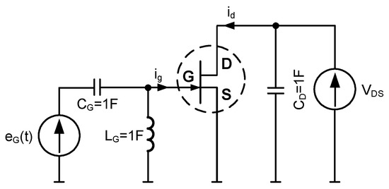
Figure 3.
Ciss measurement fixture.
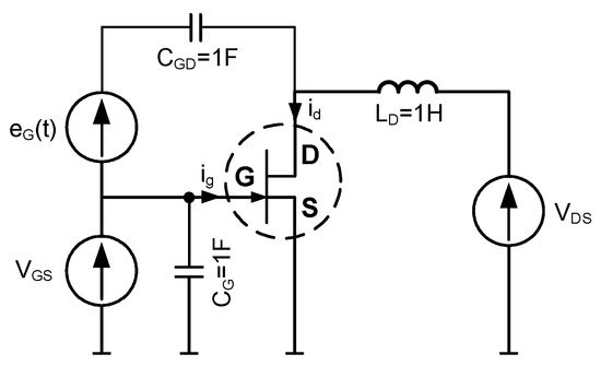
Figure 4.
Crss measurement fixture.
Capacitances CG, CD, CGD and inductances LG, LD from Figure 3 and Figure 4 with non-physical large values are used to separate appropriate currents and voltages in the fixtures. Voltage sources VGS and VDS determine the operating point of the transistor. The voltage source eG(t) generates a sinusoidal signal with an amplitude UM = 10 mV and a frequency f = 1 MHz. Capacitance values at a defined operating point are determined by performing a transient analysis and are calculated according to equations [10]:
where: ig, id, Vgs, Vgd, Vds—amplitude of alternating currents and voltages marked in Figure 3 and Figure 4.
Calculated and measured characteristics Ciss and Crss versus drain–source voltage are presented in Figure 5. Points and solid lines in Figure 5 denote the results of measurements and calculations, respectively.
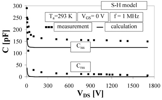
Figure 5.
Measured and calculated (S–H model) Ciss(VDS) and Crss(VDS) characteristics of the JFET.
As seen from Figure 5, there are discrepancies between the measurements and the calculations. For example, the calculated values of capacitance Ciss for the drain–source voltage up to 500 V are smaller than the values obtained from measurement by about 40%. In the range of relatively small values of drain-source voltage VDS, capacitance values decrease rapidly with the increase of the voltage VDS. However, in the range of drain-source voltage above 100 V capacitance changes are barely noticeable.
4. Modifications of the Shichman–Hodges Model
The original Shichman–Hodges model assumes [12] that the gate–source and the gate–drain junctions appearing in the transistor structure are identical in terms of physical properties and electrical parameters. Therefore, the model parameters such as M, PB and FC are used to describe properties of the junctions in common (see Equations (4)–(7)). This means that an attempt to determine the values of these parameters in order to achieve a good agreement between simulation and measurement results of the gate–drain junction automatically changes the shape of calculated gate-source junction characteristics.
On the other hand, the structure of a real JFET contains p–n junctions of different electrical properties [21], so a separate set of M, PB and FC parameters has to be used. In the proposed model, independent descriptions of each junction were introduced to increase the modelling accuracy, according to equations:
- for VGS ≤ FC1·PBCGS
- for VGS > FC1·PBCGS
- for VGD ≤ FC2·PBCGD
- for Vgd > FC2·PBCGDwhere: FC1, PBCGS, MGS, FC2, PBCGD, MGD represent a new set of model parameters.
The modified model was implemented to SPICE as a subcircuit with the use of the ABM (Analog Behavioral Modeling) option (using controlled sources). The network form of the proposed model is presented in Figure 6. Controlled-current sources GCGD and GCGS represent currents flowing through CGD and CGS capacitances. An additional parameter estimation procedure was carried out. New values of the model parameters describing the gate–source and the gate–drain junction are as follows: FC1 = 0.975, PBCGS = 2.764 V, MGS = 0.305, FC2 = 0.826, PBCGD = 2.654 V, MGD = 0.679.
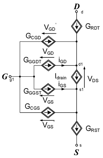
Figure 6.
Network form of the modified model of the JFET.
The results of the experimental verification of the modified model are presented in Figure 7 and Figure 8. Points and solid lines in Figure 7 and Figure 8 denote the results of measurements and calculations, respectively.
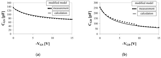
Figure 7.
(a,b) Measured and calculated (modified model) C–V characteristics of the JFET.
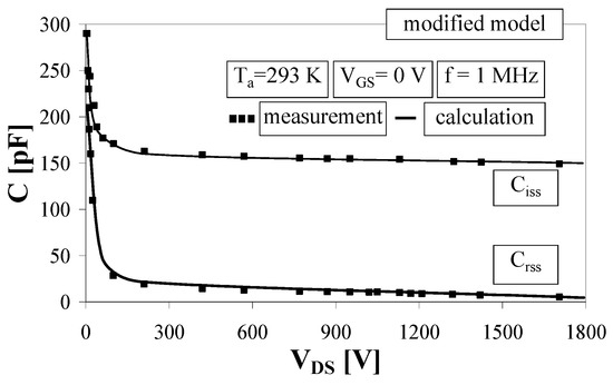
Figure 8.
Measured and calculated (modified model) Ciss(VDS) and Crss(VDS) characteristics of the JFET.
As seen, the results of modeling using the modified model provide much greater modelling accuracy than the original S–H model.
5. Simulation Results of Dynamic Characteristics of JFET
Measurements and calculations of the dynamic characteristics of the transistor were carried out in order to check the suitability of the modified JFET model. For this purpose, the simplest measurement system was chosen—a switching circuit presented in Figure 9.
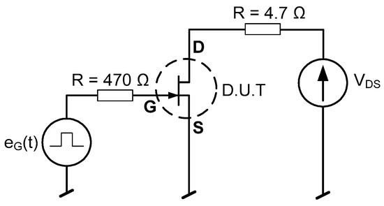
Figure 9.
Switching circuit of the transistor.
In the switching circuit, the source VDS is responsible for determining the operating point of the transistor, whereas the source eG(t) with an amplitude equal to 2.5 V and frequency of 10 kHz forces stimulation on the transistor gate.
Measurement and calculation results of VGS(t) and VDS(t) waveforms of the JFET are presented in Figure 10. Points and solid lines in Figure 10 denote the results of measurements and calculations, respectively.
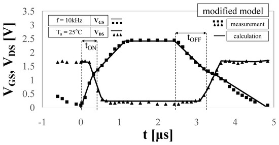
Figure 10.
Calculated and measured time waveforms of the gate–source and drain–source voltage of the JFET in the switching circuit.
A good agreement between the results of measurements and calculations of waveforms VGS(t) and VDS(t) is observed, which confirms the correctness of the modified model. The turn-on (tON) and turn-off (tOFF) delay times of the transistor are equal to about 0.3 and 0.8 µs, respectively.
6. Conclusions
In this paper, the usefulness of the Shichman–Hodges model of the JFET built-in in SPICE is examined. The SJEP170R550 transistor offered by SemiSouth Inc. is considered in detail. Owing to the observed discrepancies between the device’s simulated and measured characteristics some modifications of the model to improve its accuracy are proposed. The modifications concern a change in the description of the capacitances of the transistor’s p–n junctions. A significant increase in the modeling accuracy of SiC JFET characteristics is observed, which confirms the validity of the modified model. The proposed model can be used for modelling other types of JFETs made of silicon carbide, where performing an estimation procedure of transistor model parameters is only required.
Author Contributions
Investigation, K.B., D.B. and J.Z.; Methodology, K.B., D.B. and J.Z.; Supervision, J.Z.; Writing—original draft, K.B., D.B. and J.Z.; Writing—review & editing, K.B., D.B. and J.Z. All authors have read and agreed to the published version of the manuscript.
Funding
This research was funded by the program of the Ministry of Science and Higher Education called “Regionalna Inicjatywa Doskonałości” in the years 2019–2022, the project number 006/RID/2018/19, the sum of financing 11 870 000 PLN.
Conflicts of Interest
The authors declare no conflict of interest.
References
- Salah, T.B.; Khachroumi, S.; Morel, H. Characterization, Modeling and Design Parameters Identification of Silicon Carbide Junction Field Effect Transistor for Temperature Sensor Applications. Sensors 2010, 10, 388–399. [Google Scholar] [CrossRef] [PubMed]
- Wang, L.; Yang, J.; Ma, H.; Wang, Z.; Olanrewaju, K.O.; Kerrouche, K.D.E. Analysis and Suppression of Unwanted Turn-On and Parasitic Oscillation in SiC JFET-Based Bi-Directional Switches. Electronics 2018, 7, 126. [Google Scholar] [CrossRef]
- Fernández-Martínez, P.; Flores, D.; Hidalgo, S.; Jordà, X.; Perpiñà, X.; Quirion, D.; Ré, L.; Ullán, M.; Vellvehí, M. A New Vertical JFET Power Device for Harsh Radiation Environments. Energies 2017, 10, 256. [Google Scholar] [CrossRef]
- Yang, J. A Silicon Carbide Wireless Temperature Sensing System for High Temperature Applications. Sensors 2013, 13, 1884–1901. [Google Scholar] [CrossRef] [PubMed]
- She, X.; Huang, A.Q.; Lucía, Ó. Review of Silicon Carbide Power Devices and Their Applications. IEEE Trans. Ind. Electron. 2017, 64, 8193–8205. [Google Scholar] [CrossRef]
- Chinthavali, M.; Ning, P.; Cui, Y.; Tolbert, L.M. Investigation on the Parallel Operation of Discrete SiC BJTs and JFETs. In Proceedings of the 2011 26th Annual IEEE Applied Power Electronics Conference and Exposition (APEC), Fort Worth, TX, USA, 6–11 March 2011. [Google Scholar] [CrossRef]
- Grekov, A.; Chen, Z.; Santi, E.; Hudgins, J.; Mantooth, A.; Sheridan, D.; Casady, J. Parameter Extraction Procedure for High Power SiC JFET. In Proceedings of the 2019 IEEE Energy Conversion Congress and Exposition, San Jose, CA, USA, 20–24 September 2009. [Google Scholar] [CrossRef]
- Funaki, T.; Kimoto, T.; Hikihara, T. Evaluation of capacitance-voltage characteristics for high voltage SiC-JFET. IEICE Electron. Express 2007, 4, 517–523. [Google Scholar] [CrossRef]
- Ding, H.; Liou, J.J.; Cirba, C.R.; Green, K. An improved junction capacintance model for junction field-effect transistors. Solid State Electron. 2006, 50, 1395–1399. [Google Scholar] [CrossRef]
- Bargieł, K.; Bisewski, D. Evaluation of Accuracy of SiC-JFET Macromodel. Computer Applications in Electrical Engineering. In Proceedings of the ITM Web Conference, Poznań, Poland, 23–24 April 2018; EDP Sciences: Julis, France, 2018; Volume 19, p. 01027. [Google Scholar] [CrossRef][Green Version]
- Wang, L.; Yang, J.; Ma, H.; Wang, Z.; Olanrewaju, K.O.; Wheeler, P. Analysis and Modeling of SiC JFET Bi-Directional Switches Parasitic Oscillation. IEEE Trans. Power Electron. 2018, 34, 8613–8625. [Google Scholar] [CrossRef]
- PSPICE A/D Reference Guide, version 10.0; Cadence Design Systems Inc.: San Jose, CA, USA, June 2003.
- Kong, M.; Hou, Y.; Yi, B.; Chen, X. A High Speed High Voltage Normally-off SiC Vertical JFET Power Device. In Proceedings of the 2019 IEEE International Conference on Electron Devices and Solid-State Circuits (EDSSC), Xi’an, China, 12–14 June 2019. [Google Scholar] [CrossRef]
- Hsu, F.-J.; Yen, C.-T.; Hung, C.-C.; Lee, C.-Y.; Lee, L.-S.; Chu, K.-T.; Li, Y.-F. High Accuracy Large-Signal SPICE Model for Silicon Carbide MOSFET. In Proceedings of the 2018 IEEE 30th International Symposium on Power Semiconductor Devices and ICs (ISPSD), Chicago, IL, USA, 13–17 May 2018. [Google Scholar] [CrossRef]
- Wang, J.; Liang, S.; Deng, L.; Yin, X.; Shen, Z.J. An Improved SPICE Model of SiC BJT Incorporating Surface Recombination Effect. IEEE Trans. Power Electron. 2019, 34, 6794–6802. [Google Scholar] [CrossRef]
- Zarębski, J.; Górecki, K. Nonlinear Compact Thermal Model of Power Semicondactor Devices. IEEE Trans. Compon. Pack. Technol. 2010, 33, 643–647. [Google Scholar] [CrossRef]
- Szelągowska, J.; Zarębski, J. Measurement and Calculations of Capacitances of BJT and SJT Made of Silicon Carbide. Computer Applications in Electrical Engineering. In Proceedings of the ITM Web Conference, Poznań, Poland, 23–24 April 2018; EDP Sciences: Julis, France, 2018; Volume 19, p. 01026. [Google Scholar] [CrossRef][Green Version]
- Górecki, K.; Górecki, P. Modelling a Switching Process of IGBTs with Influence of Temperature Taken into Account. Energies 2019, 12, 1894. [Google Scholar] [CrossRef]
- Bargieł, K.; Bisewski, D. DC characteristics of power SiC-JFET. Prz. Elektrotechniczny 2018, 94, 63–66. [Google Scholar] [CrossRef]
- Bargieł, K.; Zarębski, J.; Bisewski, D. SPICE-Aided Modeling of High-Voltage Silicon Carbide JFETs. In Proceedings of the 39th International Microelectronics and Packaging Poland Conference (IMAPS), Gdansk, Poland, 20–23 September 2015; IOP Conference Series-Materials Science and Engineering. Curran Associates, Inc.: Red Hook, NY, USA, 2016; Volume 104. [Google Scholar] [CrossRef]
- Alonso, A.R.; Diaz, M.F.; Lamar, D.G.; Perez de Azpeitia, M.A.; Hernando, M.M.; Sebastian, J. Switching performance comparison of the SiC JFET and SiC JFET/Si MOSFET cascode configuration. IEEE Trans. Power Electron. 2014, 29, 2428–2440. [Google Scholar] [CrossRef]
- Rondon-Pinilla, E.; Morel, F.; Vollaire, C.; Schanen, J.-L. Modeling of buck converter with a SiC JFET to predict EMC conducted emissions. IEEE Trans. Power Electron. 2014, 29, 2246–2260. [Google Scholar] [CrossRef]
- Li-Gang, R.; Ping, Z.; Li, W. Data Driven Modeling and Verification for Silicon Carbide JFET with Thermal Effects. In Proceedings of the 2014 IEEE Applied Power Electronics Conference and Exposition—APEC, Fort Worth, TX, USA, 16–20 March 2014; pp. 2649–2653. [Google Scholar] [CrossRef]
- Cai, C.; Qu, Y.; Guo, Q.; Tao, W.; Sheng, K. Parameters Evaluation for SiC-JFET Modeling Considering Non-Uniformity by Fabrication. In Proceedings of the 2012 IEEE International Symposium on Industrial Electronics, Hangzhou, China, 28–31 May 2012; pp. 437–441. [Google Scholar] [CrossRef]
- Available online: http://www.farnell.com/datasheets/1696883.pdf (accessed on 22 December 2019).
- Bisewski, D. Parameters Estimation of SPICE Models for Silicon Carbide Devices. In Proceedings of the 2017 IEEE 21st European Microelectronics and Packaging Conference (EMPC) & Exhibition, Warsaw, Poland, 10–13 September 2017. [Google Scholar] [CrossRef]


© 2020 by the authors. Licensee MDPI, Basel, Switzerland. This article is an open access article distributed under the terms and conditions of the Creative Commons Attribution (CC BY) license (http://creativecommons.org/licenses/by/4.0/).