Article

AC “Back to Back” Switching Device in Industrial Application †

1
Department of Energy, Politecnico di Milano, 20156 Milan, Italy
2
School of Technology and Innovations, Electrical Engineering, University of Vaasa, 65200 Vaasa, Finland
3
Dipartimento di Fisica, Università degli Studi di Milano, 20133 Milan, Italy
*
Author to whom correspondence should be addressed.
This paper is an extended version of our paper published in 2018 IEEE International Conference on Environment and Electrical Engineering and 2018 IEEE Industrial and Commercial Power Systems Europe (EEEIC/I&CPS Europe), Palermo, Italy, 12–15 June 2018; doi:10.1109/EEEIC.2018.8494482.
Energies 2020, 13(14), 3539; https://doi.org/10.3390/en13143539
Submission received: 13 May 2020 / Revised: 22 June 2020 / Accepted: 29 June 2020 / Published: 9 July 2020
(This article belongs to the Section F: Electrical Engineering)

Abstract

:
In industrial applications, among several varieties of semiconductor devices available, a silicon-controlled rectifier (SCR) is often used in managing and protecting various systems with different applications. Hence, it is of the utmost importance to design a control system which can operate over a range of electrical loads without any modifications in its hardware and/or software. This paper analyzes and investigates in detail the power circuit effects on conduction delay and SCR functioning. Moreover, two different commonly used driving systems for SCR application have been introduced, discussed, and evaluated. Concerning driving systems, here, three aspects have paramount importance and are consequently taken into consideration, namely the driver system losses, the conduction delay, and in particular, some power quality indices. The conduction delay is a parameter of great importance, as being able to control and reduce it to the minimum allowed by the application can bring significant practical advantages (both in terms of application and economic terms, as better summarized in the article). Theoretical analysis has been performed, followed and verified by simulation studies and, for some cases, laboratory experimental test results are presented which provide credibility to the study.

1. Introduction

In industrial applications, the silicon-controlled rectifier (SCR) (power electronics-based switch and breaker) is a widely-used semi-controlled device due to its controllability and flexibility over diodes (uncontrolled switches) and its reliability and affordable prices with respect to fully-controlled power electronic switches [1,2,3,4]. Moreover, in diverse industrial fields, among several varieties of semiconductor devices available, SCRs are a preferred choice in managing and protecting various systems with different applications, especially in the field of industrial control systems [5,6,7] where it is mandatory to consider the peak value of current and its duration. As examples, in magnetic applications (where the magnets are sensitive to the peak current) and electric protection devices, it is of importance to take into account the peak current value, its shape and its time duration, else it might result in the damage of the system [8] and/or the protected load.
SCR due to its characteristics (controllability, reliability, and affordable price) is the first choice in several other industrial applications as well [4]. Controllability refers to the ability to move the system or the device (as it is in this situation) in the proper way as desired and in its entire configuration space using only certain admissible manipulations (as it will be clear in the following). Reliability, instead, is the ability of an item to perform the required function under given conditions for a given time interval. Finally, components should be evaluated also taking into account the cost versus the given functions.
Flexible AC transmission systems (FACTS) is a wide area where SCRs are often used, particularly in Static VAR compensators (SVC) which are utilized in different sectors in electric power system (distribution and transmission lines/substations). Authors in [9] comprehensively reviewed the applications of SVC in different positions in electric railway systems. The evolution of SVC led to the development of static synchronous compensator (STATCOM), where in many topologies SCRs are still being used due to its economic benefits [10].
SCRs have also found their applications in high voltage DC (HVDC) systems, where they act as a converter interface between AC and DC systems and provides smooth operation through phase-control. Other interesting applications, which are under development include a hybrid DC vacuum circuit breaker for medium voltage and is reported in [11]. A self-supplied SCR for medium voltage application for a solid-state starter is proposed in [12].
In addition, Phase-controlled converters in high power AC machine drives is another vast field of application for SCRs and is a topic for many research articles. The recent works on SCR deal with the mitigation effects of common-mode current, as investigated in [13], and harmonic reduction of three-phase controlled converters, as studied in [14].
Furthermore, the wide range of applications of SCRs is not only limited to high voltage or high power. The diode triggered SCR for high temperature, low voltage electrostatic discharge application has been recently introduced and studied [15,16,17].
Given the wide range of applications of SCRs, under normal operation, a precise control to turn on the SCR (SCR conduction) and with emphasis to close the circuit at the right instant is important. In modern industrial applications, where it is mandatory to obtain high reliability with a mixture of optimal control techniques and diagnostics (particularly techniques related to detect failures), this target can be achieved [18,19]. The study on SCR as a static switch presented in this paper is mainly focused on applications related to power quality, demand response, current management for magnetic load, and in smart grid system applications [20].
Considering that the only way to properly use a SCR is to utilize an electronic control circuit, it is of utmost importance to design an universal SCR driver system which, without any modifications in its hardware and/or software, can operate over a wide variety of applications [21,22], and in turn, it can achieve optimal functionality and high level of system reliability [23].
In order to achieve this goal, it is important to understand the device behaviour and investigate different factor’s (e.g., supply voltage or load characteristics, and driver control circuit characteristics) effects on SCRs ignition. Although the behaviour of the SCR itself is familiar for the scholars and engineers in the field, the effects of different elements on SCR operation have not been studied or reported in any publication. These effects on SCR ignition reported in this paper, are very essential to design an effective control system which can operate over wide range of applications minimizing the SCRs side effects.
This paper fill-in the gaps existing in current literature and investigates in detail the issues in general format and formulate the minimum pulse duration for ignition of an SCR as function of electrical parameters and different driver topologies, in order to lead to a system with better controllability, higher power quality, and to minimize design efforts to allow the industry to reuse a solution in several applications with minor or no changes.
The paper is an extended version of previous work [24] and is organized in the following way. In Section 2, a general review of SCR devices and its application is given. In Section 3, the problem formulation is explained considering both general and practical aspects. In Section 4, we provide evidence concerning the driver circuits used, the simulation, and the obtained experimental results are discussed. Finally, the conclusions are summarized in Section 5.

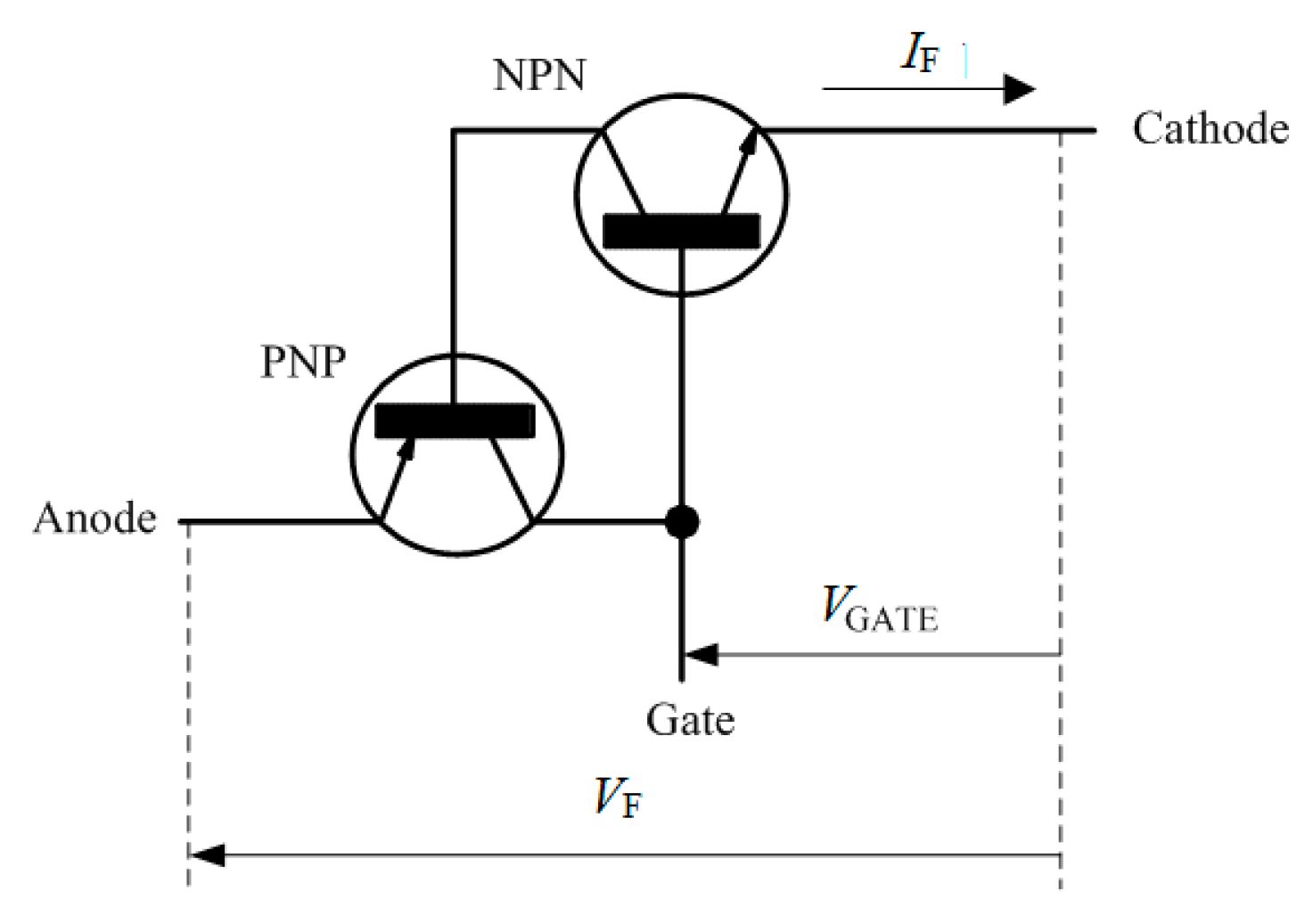
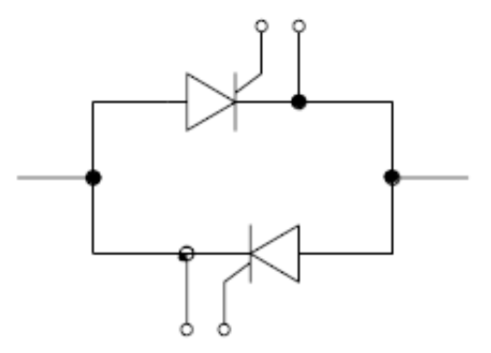
2. An Overview on SCR and Its Application

SCR is a semiconductor device widely used as a power switch. Its usage over the years increased due to its characteristics of fast switching current, during switch on and sometimes during switch off, in comparison to the more traditional and historically used electromechanical breaker.
The switching on of the device can be controlled with a gate signal by means of well-defined biasing conditions. Through this, the electrical parameters of the load voltage, current, and average absorbed power by load can be controlled.
The SCR device is typically manufactured by four layers of P and N type semiconductor materials placed one after another in alternating fashion. The operation of the SCR can be explained by a pair of tightly coupled bipolar junction transistors, arranged in such a way to cause a self-latching action as depicted in Figure 1. Here, two transistors are shown, namely PNP and an NPN devices.
When the VGATE is positive with respect to the cathode, the SCR operates in its forward characteristics. Figure 2 graphically reports SCR’s forward characteristics. In Figure 2, three I-V curves are plotted in order to show gate current (designated as IG) effects on SCR’s forward voltage (reported on abscissa axis) and the forward current (reported on the ordinate axis). In particular it represents three curves covering IG = 0, relatively low gate current (IG1) and slightly higher gate current (IG2). It can be noticed that I-V cures follow a similar shape unless the breakover point occurs sooner with higher IG.
In Figure 3, the qualitative variation of Forward Breakdown Voltage (VB0) vs. Gate Current (IG) is shown. It puts in evidence that the correct way to turn on a SCR, is to apply a fast current pulse with suitable amplitude to the gate terminal when a positive voltage is provided between anode and cathode in order to reduce the breakover voltage of the device.
Therefore, the gate current is usually made high enough to ensure that the SCR is switched to the ON state at the proper time and it is usually necessary for just an instant because a constant gate current is not required to trigger the SCR and it would only cause more power losses that needs to be dissipated within the device. Therefore, once the device has been switched-on by the gate terminal, it remains latched in the ON state and it does not need a continuous supply of gate current in order to maintain the conduction. This is true only if the anode current has exceeded the latching current (denoted by IL in Figure 2).
As long as the anode remains positively biased, it cannot be switched off until the anode current falls below the holding current (denote as IH) and so the voltage across the SCR become zero or negative.
After the current has reached natural zero point, a finite amount of time delay is required before initiating another switch on procedure and during this period SCR must retain in off state. This minimum time delay is called turn off time (tQ).
To have right SCR gate triggering, following conditions need to be provided:
an appropriate gate to cathode voltage (VGATE) is needed to turn on the device while the SCR is forward biased;
gate signal shall be removed after the device under test is turned on in order to reduce the losses and avoid higher junction temperature;
while the device is in reverse biased conditions, no VGATE signal should be applied;
when the device is in-off state, negative VGATE should be applied to improve the performance of the under-test device.
Taking into account the above considerations and noticing that the pulses must occur periodically (considering the network frequency), it is evident that the gate is triggered by means of a pulsed waveform applied across the gate terminals and will be able to work correctly for all the power switch applications and with any load conditions. Therefore, it is very important to know the availability of SCR topologies in the market. Based on the manufacturing technology used, three different topologies of SCR can be realized—they are listed below and are described in more detail in the literature, e.g., in [25]:
Planar type: Typically used for low current devices because the junctions are obtained by diffusion and come to the same surface on the cathode side. The ratio silicon/ampere is typically high;
Mesa type: It is used for high current devices but low di/dt ratio. Power SCRs are typically manufactured by this process;
Press pack type: Widely used in applications where it is necessary to have SCR with center gate and large value of di/dt.
Usually, power SCRs use a Mesa process for manufacturing. It is important to note that the device is prevalently used in “back to back” mode in AC circuit configurations, see Figure 4 where the device is turned off automatically, hence load current is cutoff every zero crossing of the signal. For the DC applications, an ad hoc circuit is necessary for the use of SCR, this is important to force the device into turn off state. However, the SCR application in DC systems is not further developed in this paper as it focuses only on AC applications.
As it can be seen from Table 1, different commercial devices available have different latching currents IL (in Table 1 the holding currents IH are also reported), therefore, it is very important to evaluate the minimum pulse time duration to be given to an SCR for its ignition. This duration is fundamental to using SCRs as switching devices in different industrial applications, because having knowledge only on latching currents (IL) is not sufficient to assure proper operation of SCR in all conditions.
Indeed, the minimum value of IL depends on the adopted delay angle control α, load impedance and on the RMS value of the applied voltage. Considering these points, in most of industrial solutions, the driving pulses length are oversized in time. Hence, the triggering pulse width is much longer than the actual width needed to guarantee the device turning on with a driving signal and to achieve the desired control function. The aim of the paper is to investigate and propose an optimum solution, which can improve overall system efficiency and functionality and can be adopted in wide range of applications.
Here, it is also worth understanding a very important aspect in certain industrial applications. The conduction angle (sometimes also denoted as ignition angle) is very important as it depends on the value of the consequent current’s peak value. In some applications, for example in the case of permanent magnet systems, the state of magnetization of the system depends precisely on the peak value of the magnetizing current. To increase this peak value, with the same system, it is possible to act on the ignition angle, making it small. Therefore, the possibility of having a system that as a whole (hardware and software) is able to turn on the SCR at low conduction angles is certainly an advantage. The advantages are multiple: in terms of ampere-turns, it is therefore possible to either obtain more from the same system or to decrease ampere-turns, obtaining an undeniable advantage in economic terms by saving on material and dimensions. All of these are obviously of completely general validity even if, in the aforementioned application, it appears to be of fundamental importance to influence the competitiveness or otherwise of the adopted solution.
The obtained results could be also influenced by the type of application, the type of driver circuit, the adopted control method and, obviously, by the characteristics of the SCR used (and with this the presence and also the importance of the above discussion).
Finally, the importance of the considerations and evaluations (numerical and experimental) that are discussed in the following sections (Section 3 and Section 4) are very evident.

3. Problem Formulation: General and Practical Discussions

3.1. General Discusion

The equivalent circuit, in Figure 5, shows the typical representation of the SCR application, where two SCRs in back to back configuration are connected to an ohmic-inductive (R-L) load.
The lagging load angle, φ, is the phase displacement between load voltage and current, and its expression is given by:
φ = a r c t g X R
where X is the reactance and R is the resistance of the load. The second Kirchhoff law permits to write the expression illustrate below:
v ( t ) = R · i ( t ) + L ( t ) · d i ( t ) d t + i ( t ) · d L ( t ) d t
where L is the inductive part of the load. Note that, in many applications, the last term of Equation(2) can be discarded because it represents the dependency of the inductance to the time variation, which it is either very low in magnitude or very slow (different time domain) comparing to electrical current’s dynamic. Ignoring the last term and solving the previous equation, the current expression can be obtained:
i ( t ) = 2 · V Z · s e n ( ω · t φ ) 2 · V Z · s e n ( α φ ) · e t α ω τ
where:
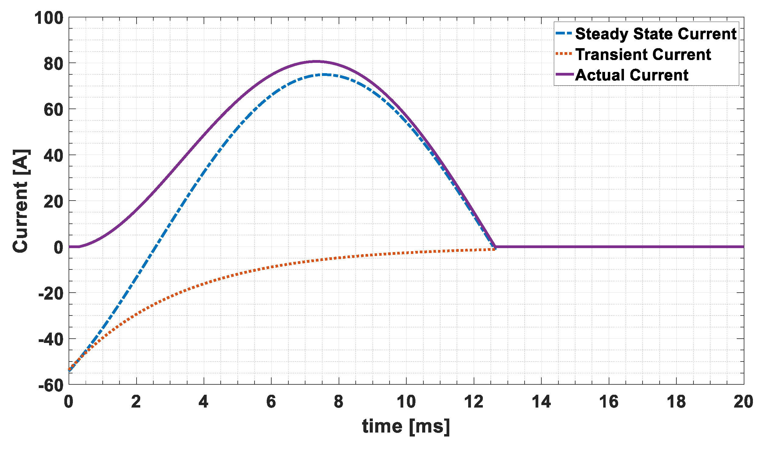
i(t) is the sum of a regimen term (first term) and a transient one (second term), which depends on time constant τ equal to L/R;
V is the rms voltage value applied by the voltage source, v(t);
Z is the load impedance;
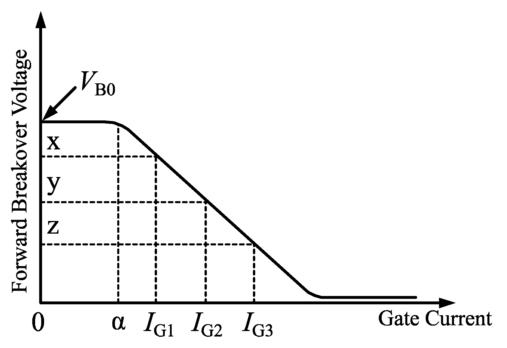
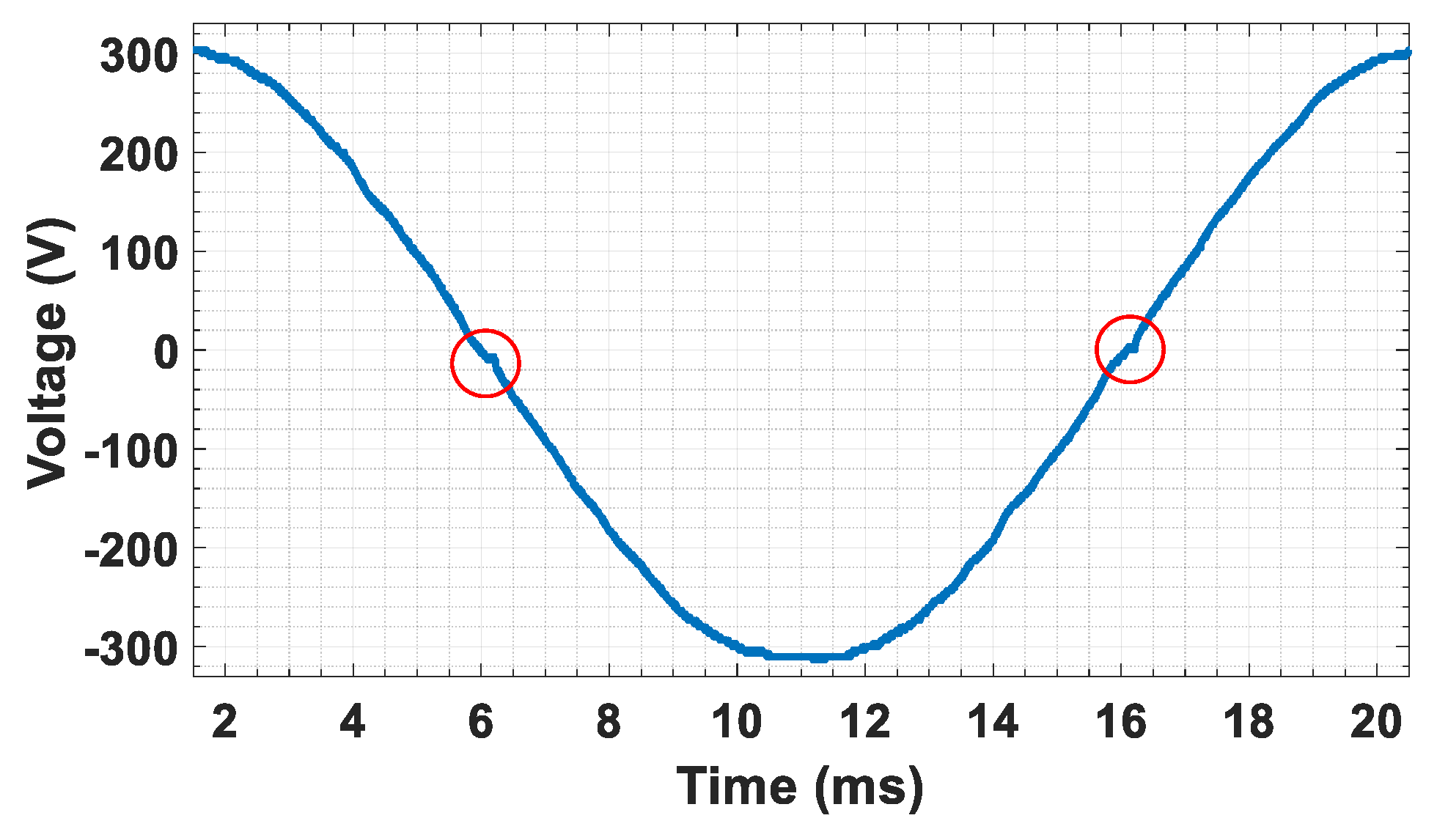
α is the control phase angle evaluated starting from the voltage zero crossing and it can be managed by the gate driver circuit often triggered through a supervisory microcontroller.
Figure 6 decomposes the current expression in (3). Here, it is possible to observe both the initial transient component and the regime (steady-state) components of the current. During the first instants, the two components have close values, but considering the negative polarity of the transient component in (3), the results of the Equation (3) are about null at starting point, which can be in the range of the driver pulse duration. In this situation, the SCR ignition can be very difficult, and it is possible not to reach required IL and fail to gain the control of SCR.
Considering this problem, it should be possible to evaluate the necessary time (tα+) for the current to reach the latching current IL by inversing (3). Given the complexity and nonlinearity of the Equation (3), it is necessary to simplify it to obtain the desired result. In particular simplified expressions of the elements e t α ω τ and s e n ( ω · t φ ) as reported in the following expressions (obtained from the MacLaurin series expansion).
e t α ω τ = e x = 1 x + x 2 2 ! + x 3 3 ! + ( 1 ) n · x n n ! +   s e n ( ω · t φ ) = s e n ( x ) = x x 3 3 ! + x 5 5 ! + ( 1 ) n · x 2 · n + 1 ( 2 · n + 1 ) ! +  
It can be seen that when the conduction starts, the element e t α ω τ can be simplified by the first two elements of the MacLaurin series, while the term s e n ( ω · t φ ) can be simplified, by the first element of the MacLaurin series, only when the value of it is close to zero.
Considering only the first elements of the MacLaurin series and using a time shift of α (t′ = t-   α ω ), the following simple expression of the current reported in (5) is obtained.
i ( t ) = 2 · V Z · ( ω · t + α φ ) 2 · V Z · s e n ( α φ ) · ( 1 t τ )
Expression (5) provides the possibility to evaluate the time t′, which is the time required to reach a specified current i(t′). Simply replacing i(t) equal to latching current IL it is possible to obtain the time required by the system to reach IL current and it will result in Expression (6):
t = I L · Z 2 · V + s e n ( α φ ) α + φ ω + s e n ( α φ ) τ
It is to be noted that expression (6) is applicable only when the conduction starts close to the point where the elements s e n ( ω · t φ ) is close to zero. In the case where this element value is far from zero, it is necessary to adopt a different approach to compute the desired time value. In this study, in order to obtain this time value, Expression (3) is simulated in a dedicated simulation software and corresponding time required to reach the latching current (IL) is extracted.
In order to represent the proposed approach, the values of delay angle α is varied between 0 and 10 ms considering a load with R = 10 Ω, L = 55 mH (typical values for the considered application), V = 230 V, f = 50 Hz (standard industrial values for Europe), and IL = 0.4 A (typical value for high current SCR devices, as described in Table 2), in order to evaluate the minimum theoretical gate pulse duration as reported in Table 2. It can be noticed that, for an example pulse duration of 200 μs, in some cases denoted with “/” the strategy works and the pulse duration is enough to ignite the SCR however in some other cases denoted by “X” the pulse duration of 200 μs is not enough to ignite the SCR.
If similar analysis is applied to different load configurations, it is easy to identify critical situations as reported in Figure 7 where, the load value highly influence the minimum value of the necessary gate pulse and in particular when it has correspondence with the zero of the voltage. It is also clear that high voltage values allow the current to quickly gain to the latching current of the SCR. For the same situation, a lower value of the voltage leads to opposite effects.

3.2. Detail and Practical Discussions

In order to optimally design an SCR control system, it is necessary to size the control system to operate on different applications without a change in its hardware topology and/or software paradigm. To achieve this, it is fundamental to know the application and corresponding load characteristics.
In some cases, especially when the load current needs to be unidirectional, as happens in electromagnetic applications, the control phase angle α can be higher or lower compared to the load angle φ, as in the example of Figure 6. Meanwhile, in other cases, such as for AC protection systems, the control phase angle α can only take values higher than that of the load angle φ.
Moreover, in some applications, there is a strong variation of the inductance during the activation/deactivation cycles. This situation is common in applications where the load changes its magnetic state. An example of aforementioned situation occurs in electrical motor during the startup, where the current rise to a very high value and reaches the steady state in the end. Many such cases of the described situation can be also found in equipment with permanent magnets. Many different applications which uses permanent magnets are found in the literature, in particular concerning the permanent magnet motors and related applications [26,27,28,29,30,31,32,33].
An interesting load, where it is possible to find both the previously mentioned problems is the electro permanent magnet (EPM). An EPM is a device realized by permanent magnets that can be switched -on or -off by a small amount of unidirectional current applying to its internal winding coil. The main applications of the EPMs are in handling of heavy ferromagnetic loads, such as iron bars and steel plates for manipulations over extended period of time, and for fixing the position of different mechanisms. In this application, the driving current is necessary only for few seconds during the activation (EPM is magnetized starting from an initial state of demagnetization) and deactivation cycles (initially magnetized EPM needs to be demagnetized). Thanks to this functionality, EPM can be considered as a system with zero electrical energy losses during working phases as described in [34].
As described, EPM needs unidirectional current, and during the activation/deactivation cycles the inductance value widely changes due to the variable nature of the magnets and the ferromagnetic circuit (function of the locked ferromagnetic load).
This phenomenon leads to a variation in current patterns, pulse after pulse, with particular regard to the transient current. In these cases, the theory and the results as described above, could be no longer adequate to define the phenomenon (due to L variation). In particular, in some cases, where it is possible to predict strong variations in the value of the inductance (L), the current may vanish, or in some cases, during the initial stage of conduction of the device, a very strange and/or unexpected shape of the current can be found. This may lead to a failure of the ignition strategy of the SCR control system.
Even though a very strong variation of inductance is not so common and important in many other applications, in the loads described here, this aspect is a very important element. Normally there can be also a huge variation of the load resistance due to the very high temperature variation (around 125 °C) and it can vary the resistance up to 50% of its nominal value.
In order to understand the impact on minimum pulse time duration due to several factors involved in the problem definition, in the following the sensitivity analysis results based on the procedure described in (3)–(6) has been performed with a dedicated simulation software. The presented aspects in this section are mainly general and applicable to wide range applications (at least theoretically).
According to the analytical procedure (3)–(6), four factors have an impact on minimum pulse duration time. These are applied voltage RMS value V, load impedance Z, load power angle φ and control pulse angle α.
In particular, the nominal voltage V = 230 V, impedance Z and power angle φ equal to 10 Ω and 0.64 radiant (R = 8 Ω, L = 19 mH) respectively, are considered. The analysis is performed varying one element, around its rated value, while the other elements are fixed to the nominal ones. In this analysis the value of alpha is fixed and is equal to 12.5 μs. This value is considered as reference for all the tests because the value of alpha doesn’t affect the direction of the variation trend but only the value of the minimum pulse duration time. The effect of impedance variation is evaluated considering impedance as one concrete parameter (varying amplitude and phase) and then its resistance (R) and inductance (L) are varied independently. In this way, the dependency of the minimum pulse time duration for SCR correct conduction is studied. The obtained results are reported in Figure 8 and they show that:
  • Supply voltage variation: applied voltage magnitude has linear effect on minimum pulse duration. For standard European voltage of 230 V RMS, this dependency is shown in Figure 8a with ±10% variation around nominal value in compliance with the international standard IEC 50160. It can be noticed that voltage variation has minor effect on minimum pulse time duration;
  • Impedance variation:Figure 8b shows the load impedance variation on the minimum pulse time duration with constant φ and V. The variation range is ±50%. An increase in Z means a lower current and a decrease in Z means a higher current. Therefore, it can be seen that, by increasing the load, the minimum pulse time duration required will increase, and with lower load current, wider pulses are required to guarantee the conduction;
  • Load power angle variation: with fixed Z and V, effect of load power angle variation has been studied. Figure 8c shows the effect of this variation on minimum pulse duration while the load changes from more resistive to more inductive absorbing the same RMS current. The variation range also in this case is ±50%. It can be seen that increasing the load power angle will cause increase in minimum pulse duration time. More inductive load needs pulses with longer width or in other word, with more resistive load the required pulse width for conduction become shorter;
  • Resistance variation:Figure 8d shows the effect of varying load resistance variation on minimum pulse time (t) required, with constants L and V. The variation range also in this case is ±50%. It can be noticed that increasing or decreasing the load resistance does not significantly influence the pulse duration. Therefore, it can be seen from Figure 8d that the variation in resistance doesn’t have a major influence on the required pulse duration;
  • Inductance variation:Figure 8e shows the effect of varying load inductance on minimum required pulse time (t), with R and V as constant values. The variation range is once again ±50%. Increasing the load inductance results in lower load current and vice versa. Hence, it can be noticed that by increasing the load inductance the minimum pulse duration needed will also increase. An aspect to note is that the variation in inductance is of very important with respect to the other parameters considered.
As it can be seen from the aforementioned analysis, the variation in resistance has no practical influence on the pulse duration, while variation in both the inductance and the applied voltage must be considered as dominant factors.
Starting from this point of view, in order to make the adopted control technique more efficient, pulse width to be considered in the gate signal should be at least equal to the sum of both variations of the inductance and voltage foreseen to the circuit under the test.
As has been observed, the problem in the choice of the ignition instant can be critical in order to obtain the desired operation and the maximization of the duration of the control pulse could introduce additional losses into the device.
When we consider the testbed consisting of the SCR circuit described in Figure 5, we arrive to the practical problem of conduction delay, which is always present. When the SCR is turned off the load is not powered by the source voltage v(t). Despite fast turn-on and turn-off characteristics, due to the inherent nature, this application introduces a short conduction delay at each voltage/current zero crossing which can be considered as distortion on load supply voltage. An example of this conduction delay is shown in Figure 9 for a resistive load.
The conduction delay can have different side effects, it affects the performance of the power circuit, interfere electromagnetically with broadband over power lines (BPL) communication devices and also deteriorates control performance of the power electronic based system [35]. Conduction delay principally depends on two main aspects concerning power circuit and SCR driver circuit. Due to the intrinsic nature, the SCR require a natural time to properly turn on, in addition to this, when the driver circuit introduces a time delay, it should be considered. If the power circuit aspect is kept unchanged, the time delay introduced by driver circuit can be analyzed in detail.

4. SCR Driver Circuits, Simulation and Experimental Results

In order to run an SCR properly, a gate signal needs to be applied for sufficient time to allow the device to latch. In a practical application, this is achieved through a driver circuit to manage the gate signal. The driver circuit can be realized either by digital microcontroller or by an analog circuit.
Two main circuit topologies to control an SCR device have been considered in this study. Both of the considered driving circuits are applied for a constant system with an SCR switch unchanged over the tests in order to compare their performance. Moreover, to compare the experimental results, both driving systems are supplied with the same voltage (equal to 15 V) and they have been controlled with the same microcontroller-based board.

4.1. Driver Circuit 1

In Figure 10, the first driver circuit is shown. In this configuration, an impulse transformer is required to control the SCR. The input (V1) has to be a high frequency pulse in order to permit the impulse transformer to work correctly with a variable signal.
It is important also to note that the pulse width duration cannot be too short, because with short pulse width, the minimum value of the latching current IL cannot be guaranteed for wide range of given load (see Table 1) and cannot be too long either because the impulse transformer works properly only with variable signals.
In general, to satisfy every load condition, it is very common to control the circuit by a series of pulses (pulse train). In this case, it is mandatory to have a minimum delay time between two successive pulses in order to de-energize the impulse transformer properly. Considering the pulses shown in Figure 11, with a pulse command of 200 μs, it is possible to observe in Figure 11a that only the first pulse can energize the impulse transformer (it can manage the ignition of the SCR). While the second and third pulses cannot reach their peak value (those cannot manage the ignition of the SCR correctly) because the pulses are too close to each other (switching frequency about 3 kHz). Considering Figure 10b, all the pulses with the same pulse command of 200 μs can energize the impulse transformer and consequently can run the SCR (switching frequency about 1.5 kHz).
In this work, pulses of 200 μs width with a frequency of 1.5 kHz is used to supply Driver Circuit 1 and control the SCR module.
A digital microcontroller is required to generate the pulses for Driver Circuit 1, in certain cases analog circuits can be used, but in general this topology can generate only a series of pulses due to the difficulty in generating the pulses at the desired moment constrained by the limitation of the impulse transformer.

4.2. Driver Circuit 2

The second driver circuit considered in this study adopts an opto-isolator to generate the pulses and manage the necessary gate current to control the SCR properly. The circuit schema is shown in Figure 12. The main difference between the Driver Circuit 2 and Driver Circuit 1, is in the gate current control philosophy. As there is no pulse transformer, it is not necessary to provide a pulse or a series of pulses. This also enables to use a constant DC voltage to ignite the SCR. The simplicity of this driving system is one of the main advantages of this topology. With this, a simple driving circuit (as simple as a push button) can be used to run the circuit. Moreover, the amount of power required to energize the circuit is quite low and hence normally the power loss is reduced.

4.3. Driver Circuit Losses Comparison

To evaluate the power losses of the driver circuits, the absorbed current ic from the control power source has to be measured in both circuits. A simple test circuit, as shown in Figure 5, is used in order to evaluate the performance of the two driver circuits. The grid voltage v(t) is 230 V at 50 Hz. The load is 1 kVA R-L load. Here, the aim is to evaluate the losses of the driver circuits. The power circuit is kept the same during both driver topology tests (to relax any possible effect), and the driver circuits are supplied with 15 V ( V D C ) voltage source.
The absorbed current from voltage source (ic) has been measured in both circuits in order to evaluate the absorbed power to manage the driver circuits. In order to measure this current, a small resistance is inserted in series to the driver circuit. This inserted resistance poses no change in the main circuit behavior. The measured voltage across the resistor (given that the ohmic value is known) represents the current in the driver circuit.
Considering that there is an impulse transformer in SCR Driver 1, the current value follows the pulses and has raising and falling edges. In order to evaluate the power for this driver circuit, the mean value of supply voltage VDC multiplied with this current (ic) is considered (7).
P l o s s e s = 1 T ·   ( V D C × i c ) d t
In (7) T is the effective average period and ic is the current absorbed from the voltage source VDC.
In case of SCR Driver 2, there is no need to supply the driver circuit with pulses, instead constant VDC = 15 V has been used. Therefore, the current can be a constant DC value. However, in order to avoid the effect of measurement noises in the evaluation of absorbed power, same analysis as in the previous case has been followed.
Table 3 reports the losses for the two driver circuits under test. As it can be noticed, SCR Driver 2 has about 25% fewer losses with respect to SCR Driver 1, because the SCR Driver circuit 2 needs a very low amount of current ic. Moreover, considering the low peak current value absorbed by SCR Driver 2 with respect to the SCR Driver 1, the components size in Driver 2 can be reduced and the overall driver circuit size can be decreased. This can also lead to more efficient and cheaper industrial design of the final product. As the opto isolator can work with very low voltage (5 V instead of 15 V) the losses of the SCR Driver 2 can be further decreased by adopting the same pulses strategy necessary for Driver 1.

4.4. Driver Conduction Delay Comparison

The conduction delay depends on control circuit, control technique, SCR topology, supply voltage RMS V, load power angle φ, (resistive, inductive or capacitive or any mix of these types), load impedance magnitude Z, and control pulse angle α. To compare the different control system, the same SCR switch for both driver circuits (so the contribution of the SCR on conduction delay is kept constant around 50 μs in both cases), and the same power circuit, as shown in Figure 5, are used. Moreover, both driving systems are supplied by the same voltage, equal to 15 V as mentioned previously, and managed with the same microcontroller board.
Here, the total conduction delays for the two different driver systems and the three different control strategies are analyzed. These different solutions can be classified according to the type of power supply:
a
SCR Driver 1 and
b
SCR Driver 2;
and/or according to the implementation control strategy:
I
gate pulse,
II
series of gate pulses,
III
constant gate signal.
These classifications are not completely independent because, as it has been discussed, it is advisable to couple a) with I) or II), and b) with III). Only in some cases is a combination of b) and I) adopted, while the combination of a) and III) cannot work.
When the gate pulse strategy (and in particular for SCR Driver 1) is adopted, the conduction delay could be more higher than the natural time delay of the SCR, especially in an EPM application that needs a unidirectional current for its proper operation and they are controlled with a control phase angle α less than the load power angle φ and very close to zero.
This can happen due to the variable nature of the load as described in the Table 4, where a load with resistance R = 1 Ω, inductance L = 50 mH, mains voltage of V = 230 V, f = 50 Hz and an SCR with IL = 0.4 A, has been considered. Cases denoted with “/” mean that the strategy works and the pulse duration is enough to ignite the SCR however in other cases denoted by “X” the pulse duration of 200 μs is not enough to ignite the SCR.
Following the theory analyzed before, the results show that the resistance variation has no practical influence on the necessary pulse duration while both the inductance variation and the applied voltage have to be considered as dominant factors. Starting from this point of view, in order to make this control technique efficient, it is mandatory to supply the gate circuit for a time at least equal to the sum of the contributions due to the variation in both the inductance and the voltage.
Therefore, in some cases, the gate pulse has to be wide enough to correctly manage the SCR, and hence this strategy can be adopted only with SCR Driver 2 and cannot be adopted by SCR Driver 1, because the impulse transformer, present in the control circuit can be saturated.
The series gate pulses strategy is used for SCR Driver 1 only, in order to increase the probability to turn-on the SCR. In some cases, the pulses are automatically generated by an analog circuit when a microcontroller is not present to manage the system. In this case, the conduction delay could be higher than the natural delay time of the SCR especially in applications such as EPM that needs unidirectional current and the control phase angle α should stay close to the zero as mentioned.
As in the previous method described, when SCR Driver 1 is driven by a series of pulses, the conduction delay is not constant, and it shows a periodic behavior. This is due to the fact that the pulse signal, which is able to set the SCR in conduction state, cannot always occur at the same moment. Therefore, the conduction delay time varies between the minimum conduction delay (few µs which depends on SCR) and the maximum one (as a function of the delay time used to correctly manage the SCR Driver 1, usually cannot be less than 700 μs). This time can increase for some load typologies, when the starting current is very close to zero and the SCR cannot be switched-on with the first pulse. So in the worst case scenario, a time delay between the two pulses can be necessary (so the delay will reach around 1.4 ms), as example a practical test is reported in Figure 13, where the distance between two pulses has been fixed higher than 700 μs, equal to 1120 μs, in order to eliminate any saturation problems of the impulse transformer.
Thus, applying this strategy to SCR Driver 1, the conduction delay will be variable, and this can produce unexpected (and unwanted) effects on other parts of the power circuit (reducing performance of the connected power electronic devices, compromising power quality level and it can also affect other electronic boards and control systems). Moreover, the variable nature of load and mains voltage may increase the uncertainties in the behavior of the SCR turn-on.
The above-mentioned conduction delay can contribute to load voltage as well as in current distortion and it can contribute to power quality issues at their connection point. Figure 14 shows an example of the distorted load voltage used for total harmonic distortion (THD) analysis and the load current in the case of a 1 kVA load with a power factor equal to 0.6 managed by a SCR in AC back to back configuration controlled by a delay of around 200 μs.
It is worth to mention that, in an ideal system, the interruptions in the voltage is expected to appears as sharp steps (shown by dashed light blue lines in the Figure 14). However, in terms of practical application, there should be a snubber circuit to limit dv/dt on SCR. The simulation results in Figure 14 are obtained using datasheet values of commercial snubber circuit SKRC 440.
Considering the complexity in evaluating the voltage and current distortions in the load, signal data analysis is made in dedicated software to extract the THD values for one case considering SCR Driver 1.
The load connected as mentioned previously is of 1 kVA and its power factor can be varied from 1 to 0.4. The signal data has been elaborated to find the THD of the load voltage. Performing the FFT analysis, the THD value has been evaluated. The voltage THD varies between the range 1.56–4.04% as expected (the minimum value can be considered the contribution of the SCR on conduction (ignition) delay that is equal to 50 μs). These values are as reported in Table 5.
Considering this strategy and Driver 1, it can be noticed that the THD is varying and, moreover, cannot be predicted. Even though the power quality indices are small and their contribution always stays within standard [36,37]. However, these are simulation results and considers only SCR effects, in a real system this distortion may be higher. The harmonic propagation will deteriorate the overall system performance which occurred as a consequence of variable conduction delay in the case of Driver 1.
Unlike SCR Driver 1, SCR Driver 2 can be managed by constant command, hence, the total conduction delay is constant and proportional to the contribution of the SCR only. In this topology, a constant DC signal can be adopted as input signal for the SCR gate signal. For the adopted SCR, this conduction delay has been recorded by laboratory test (for resistive load) and as it is reported in Figure 15. The conduction delay is constant, invariable, and equal to 50 µs (which is the time required by the SCR). To evaluate THD results, similar to previous case, simulations are performed for loads with different power factors and Table 6 reports the obtained THD results.
Comparing the two different circuit topologies, SCR Driver 1 and gate pulse or series of gate pulses strategy leads to variable conduction delay. This can cause a problem with respect to control of the power, cause issues in power quality, and can also diversely interfere in the performance and operation of other systems. SCR Driver 2 with constant gate signal has a constant conduction delay which depends only on the adopted SCR. Hence, this SCR Driver 2 does not have a power control problem and also helps in reducing power quality issues.

5. Conclusions

The aim of the paper is to analyze and investigate in detail the parameters that influence the conduction delay of an SCR used in an AC back to back controlling device in order to find a novel and generic solution enhancing the control capability of an SCR for its use in a wide range of loads in industrial applications.
The paper shows that the conduction delay depends on supply voltage magnitude V, load power angle φ, load impedance magnitude Z, and obviously control pulse angle α. In particular, it has been demonstrated that control phase angle α and load inductance L, and supply voltage are very important with respect to the other parameters on minimum pulse duration to get correct conduction of SCR. Therefore, these aspects are considered in applications such as an electro permanent magnet (EPM) that need a unidirectional current in which the control phase angle α can be close to zero and the inductance undergoes considerable variation.
Moreover, the paper introduces, evaluates, and compares two different commonly used driver circuits for SCR application through simulation and practical laboratory tests (SCR Driver 1-realized adopting an impulse transformer and SCR Driver 2 is built using an opto-isolator). Three different and widely used control strategies for these two driver topologies are presented, which include: gate pulse, series of gate pulses, and constant gate signal strategies respectively.
For comparison between the two driver circuits, three aspects are considered: driver system losses, conduction delay on load voltage due to the adopted control circuit strategy and power quality indices. SCR Driver 1 has higher losses and needs a much more complex driving signal which can be generated by digital microcontroller or by a complex analog circuit. However, SCR Driver 2 has lower operational losses, which can be realized and run by much more simple driving system.
From conduction delay point of view, SCR Driver 1 leads to a long and a variable conduction delay, while SCR Driver 2 has a short and constant conduction delay.
From power quality point of view, the system with SCR Driver 1 leads to variable THD on the load voltage with consideration of the variable nature of load. Instead, with SCR Driver 2, the THD value is almost constant. In both these cases, the THD value always lies within required value specified by the standards and the difference between these two configurations is very small.
In conclusion, we can state that SCR Driver 2, which is based on opto-isolator, shows better performance with respect to SCR Driver 1, which is based on impulse transformer. Hence, SCR Driver 2 can be recommended, since its control and performance do not depend on its control circuit.
We also recall what was previously discussed regarding the importance of minimizing the conduction angle, as minimization of the conduction angle leads to incredible advantages in all those applications in which the final effect (which is also appreciable in terms of better overall performance) is a function of the magnetizing current peak value, which is controlled by the SCR device.
These considerations reported are fully general and applicable, in all applications controlled by SCR, at least in the theoretical aspects.
To address the future research, considering at a higher level, the range of applications for an SCR can be divided into four broad fields, namely AC-AC systems (mostly the topics covered in this paper), AC-DC systems where the solutions offered in this paper should operate with no or minor changes, DC-AC systems, and DC-DC systems. In DC-AC and DC-DC systems, the application of SCR and the solutions proposed in this paper will need further investigation and research. Moreover, the novel driver circuit could be investigated. Those topics are left open for future studies.

Author Contributions

Conceptualization, Methodology, Investigation, Writing-Original Draft Preparation, Writing-Review & Editing, R.F., H.H., K.A. and M.L. All authors have read and agreed to the published version of the manuscript.

Funding

This research received no external funding.

Conflicts of Interest

The authors declare no conflict of interest.

References

  1. Isermann, R. Towards intelligent control of mechanical processes. In Control Engineering Practice; Elsevier: Delft, The Netherlands, 1993; Volume 1, pp. 233–252. ISSN 0967-0661. [Google Scholar]
  2. Tan, K.K.; Tang, K.Z.; Dou, H.F.; Huang, S.N. Development of an integrated and open-architecture precision motion control system. Control. Eng. Pract. 2002, 10, 757–772. [Google Scholar] [CrossRef]
  3. Godse, A.P.; Bakshi, U.A. Basic Electrical and Electronics Engineering; Technical Publications: Pune, India, 2007; ISBN 8184312733. [Google Scholar]
  4. Huang, A.Q. Power Semiconductor Devices for Smart Grid and Renewable Energy Systems. Proc. IEEE 2017, 105, 2019–2047. [Google Scholar] [CrossRef]
  5. Osornio-Rios, R.A.; Romero-Troncoso, R.d.J.; Herrera-Ruiz, G.; Castañeda-Miranda, R. The application of reconfigurable logic to high speed CNC milling machines controllers. Control Eng. Pract. 2008, 16, 674–684. [Google Scholar] [CrossRef]
  6. Charbonnaud, P.; Carrillo, F.J.; Ladevèze, D. Monitored robust force control of a milling process. Control Eng. Practice 2001, 9, 1047–1061. [Google Scholar] [CrossRef]
  7. Naso, D.; Cupertino, F.; Turchiano, B. Precise position control of tubular linear motors with neural networks and composite learning. Control Eng. Practice 2010, 18, 515–522. [Google Scholar] [CrossRef]
  8. Faranda, R.; Lazzaroni, M. Industrial low cost temperature measurement in permanent electro-magnetic platens. Measurement 2012. [Google Scholar] [CrossRef]
  9. Wang, H.; Liu, Y.; Yan, K.; Fu, Y.; Zhang, C. Analysis of static VAr compensators installed in different positions in electric railways. IET Electr. Syst. Transp. 2015, 5, 129–134. [Google Scholar] [CrossRef]
  10. Singh, B.; Saha, R.; Chandra, A.; Al-Haddad, K. Static synchronous compensators (STATCOM): A review. IET Power Electron. 2009, 2, 297–324. [Google Scholar] [CrossRef]
  11. Liu, L.; Zhuang, J.; Wang, C.; Jiang, Z.; Wu, J.; Chen, B. A Hybrid DC Vacuum Circuit Breaker for Medium Voltage: Principle and First Measurements. IEEE Trans. Power Deliv. 2015, 30, 2096–2101. [Google Scholar] [CrossRef]
  12. Raonic, D.M. SCR self-supplied gate driver for medium-voltage application with capacitor as storage element. IEEE Trans. Ind. Appl. 2000, 36, 212–216. [Google Scholar] [CrossRef]
  13. Patel, Y.P. Mitigation of the Effects of Common-Mode Current on the Operation of SCR-Based Rectifiers for AC Drives. IEEE Trans. Ind. Appl. 2016, 52, 4827–4834. [Google Scholar] [CrossRef]
  14. Eltamaly, A.M. Harmonic injection scheme for harmonic reduction of three-phase controlled converters. IET Power Electron. 2018, 11, 110–119. [Google Scholar] [CrossRef]
  15. Chen, J.T.; Ker, M.D. ESD Protection Design with Diode-Triggered Quad-SCR for Separated Power Domains. IEEE Trans. Device Mater. Reliab. 2019, 19, 283–289. [Google Scholar] [CrossRef]
  16. Liu, W.; Liou, J.J.; Yeh, H.C.; Wang, H.; Li, Y.; Yeo, K.S. Bidirectional diode-triggered silicon-controlled rectifiers for low-voltage ESD protection. IEEE Electron Device Lett. 2012, 33, 1360–1362. [Google Scholar] [CrossRef]
  17. Junxiong, G.; Jizhi, L.; Rui, T.; Liu, Z.; Zhiwei, L. Novel Diode-Triggered Silicon-Controlled Rectifier (DTSCR) for High-Temperature Low-Voltage Electrostatic Discharge (ESD) Applications. In Proceedings of the 2016 IEEE International Nanoelectronics Conference (INEC), Chengdu, China, 9–11 May 2016; pp. 1–2. [Google Scholar] [CrossRef]
  18. D’Antona, G.; Faranda, R.; Hafezi, H.; Accetta, G.; Della Giustina, D. Open UPQC: A possible solution for customer power quality improvement. Shunt unit analysis. In Proceedings of the Harmonics and Quality of Power (ICHQP), 2014 IEEE 16th International Conference, Bucharest, Romania, 25–28 May 2014; pp. 596–600. [Google Scholar]
  19. D’Antona, G.; Faranda, R.; Hafezi, H.; Accetta, G.; della Giustina, D. Open UPQC: A possible solution for power quality. Series unit analysis. In Proceedings of the Power Electronics, Electrical Drives, Automation and Motion (SPEEDAM), 2014 International Symposium, Ischia, Italy, 18–20 June 2014; pp. 1104–1109. [Google Scholar]
  20. D’Antona, G.; Faranda, R.; Hafezi, H.; Bugliesi, M. Experiment on Bidirectional Single Phase Converter Applying Model Predictive Current Controller. Energies 2016, 9, 233. [Google Scholar] [CrossRef] [Green Version]
  21. Govindhasamy, J.J.; McLoone, S.F.; Irwin, G.W.; French, J.J.; Doyle, R.P. Neural modelling, control and optimisation of an industrial grinding process. Control Eng. Practice 2005, 13, 1243–1258. [Google Scholar] [CrossRef] [Green Version]
  22. Abele, E.; Altintas, Y.; Brecher, C. Machine tool spindle units. CIRP Ann. Manuf. Technol. 2010, 59, 781–802. [Google Scholar] [CrossRef]
  23. Cardone, M.; Cosmai, G.; Faranda, R.; Giglio, A. Modular Magnetic Device for Clamping Ferromagnetic Workpieces. U.S. Patent 8,957,750, 21 August 2014. [Google Scholar]
  24. Faranda, R.; Hafezi, H.; Karakasli, V.; Ingrao, M.; Lazzaroni, M. AC "Back to Back" Switching Protection in Inductive Application. In Proceedings of the 2018 IEEE International Conference on Environment and Electrical Engineering and 2018 IEEE Industrial and Commercial Power Systems Europe (EEEIC/I&CPS Europe), Palermo, Italy, 12–15 June 2018; pp. 1–6. [Google Scholar]
  25. Bakshi, U.A.; Godse, A.P. Elements of Electronics Engineering; Technical Publications: Pune, India, 2008; p. 476. ISBN 818431292X. [Google Scholar]
  26. Lee, T.-S.; Lin, C.-H.; Lin, F.-J. An adaptive H∞ controller design for permanent magnet synchronous motor drives. Control Eng. Practice 2005, 13, 425–439. [Google Scholar] [CrossRef]
  27. Yousefi, H.; Hirvonen, M.; Handroos, H.; Soleymani, A. Application of neural network in suppressing mechanical vibration of a permanent magnet linear motor. Control Eng. Practice 2008, 16, 787–797. [Google Scholar] [CrossRef]
  28. Zhao, S.; Tan, K.K. Adaptive feedforward compensation of force ripples in linear motors. Control Eng. Practice 2005, 13, 1081–1092. [Google Scholar] [CrossRef]
  29. Wu, D.; Chen, K. Design and Analysis of Precision Active Disturbance Rejection Control for Noncircular Turning Process. IEEE Trans. Ind. Electron. 2009, 56, 2746–2753. [Google Scholar]
  30. Yang, Y.; Gao, F. Adaptive control of the filling velocity of thermoplastics injection molding. Control Eng. Practice 2000, 8, 1285–1296. [Google Scholar] [CrossRef]
  31. Konrad, H. Fault detection in milling, using parameter estimation and classification methods. Control Eng. Practice 1996, 4, 1573–1578. [Google Scholar] [CrossRef]
  32. Tsai, C.-C.; Lin, S.-C.; Wang, T.-Y.; Teng, F.J. Stochastic model reference predictive temperature control with integral action for an industrial oil-cooling process. Control Eng. Practice 2009, 17, 302–310. [Google Scholar] [CrossRef]
  33. Sánchez, R.; Aisa, J.; Martinez, A.; Mercado, D. On the relationship between cooling setup and warpage in injection molding. Measurement 2012, 45, 1051–1056. [Google Scholar] [CrossRef]
  34. Cardone, M.; Faranda, R.; Giglio, A.; Foglia, G.; Moroni, E. Safety Device in Magnetic Locking System for Moulds; MACPLAS International (Technical Magazine for the Plastics and the Rubber Industry); Promaplast Srl: Assago, Italy, 2006; pp. 31–34. ISSN 0394-3453. [Google Scholar]
  35. Faranda, R.; Dezza, F.C.; Mazzucco, I.; Redi, P.; Tironi, E. An interface converter for DG/storage system able to improve Power Quality of the load. In Proceedings of the IEEE Power Engineering Society PES, Montreal, QC, Canada, 18–22 June 2006. [Google Scholar]
  36. Hafezi, H.; Faranda, R. Power quality and custom power: Seeking for a common solution in LV distribution network. In Proceedings of the 2017 IEEE International Conference on Environment and Electrical Engineering and 2017 IEEE Industrial and Commercial Power Systems Europe (EEEIC/I&CPS Europe), Milan, Italy, 6–9 June 2017. [Google Scholar]
  37. IEEE Recommended Practice and Requirements for Harmonic Control in Electric Power Systems. In IEEE Std 519-2014 (Revision of IEEE Std 519-1992); June 2014. [CrossRef]
Figure 1. SCR equivalent circuit. The operation of the SCR can be simply explained by a pair of tightly coupled bipolar junction transistors, arranged as in figure in such a way to cause a self-latching action.
Energies 13 03539 g001
Figure 2. Different kind of SCR Static I-V Characteristics (qualitative representation, not in scale). Legend: VB0 = Forward Breakover Voltage, VBR = Reverse Breakover Voltage, IG = Gate Current, IL = Latching Current, IH = Holding Current.
Energies 13 03539 g002
Figure 3. Qualitative variation of Breakdown Voltage (VB0) vs. Gate Current (IG): the correct way to turn on a SCR device is to apply a fast current pulse with suitable amplitude on the gate terminal when a positive voltage is applied between anode and cathode to reduce the Breakover Voltage of the device.
Energies 13 03539 g003
Figure 4. The AC “Back to Back” Switch configuration.
Energies 13 03539 g004
Figure 5. Equivalent circuit of SCR application for R-L load: two SCRs in back to back configuration are connected to an ohmic-inductive (R-L) load.
Energies 13 03539 g005
Figure 6. Simulated shape of the current.
Energies 13 03539 g006
Figure 7. Minimum ignition time variation for different loads at V = 230 V and f = 50 Hz.
Energies 13 03539 g007
Figure 8. Minimum time duration in function of (a) main voltage V, (b) Z load, (c) φ load, (d) R load and (e) L load variation.
Energies 13 03539 g008
Figure 9. An example of practical conduction delay at zero voltage crossing for ohmic load with pulse strategy.
Energies 13 03539 g009
Figure 10. Typical circuit used for SCR drive with impulse transformer. (a) schematic circuit diagram (b) practical realization.
Energies 13 03539 g010
Figure 11. Impulses with a frequency of (a) around 3 kHz–problems on the second and third pulses (b) around 1.5 kHz–both pulses represented has similar behavior.
Energies 13 03539 g011
Figure 12. Typical circuit used for SCR drive with opto-isolator. (a) schematic circuit diagram (b) the practical realization.
Energies 13 03539 g012
Figure 13. Example conduction delay response with pulses control changing the pulse time (a) far to the natural voltage zero crossing, (b) close to the natural voltage zero crossing (both pulses happen with positive voltage and the distance between two pulses is 1.12 ms).
Energies 13 03539 g013
Figure 14. Example of load voltage and current (obtained with a 1 kVA load with power factor PF equal to 0.6) affected by a conduction delay in the AC back to back device.
Energies 13 03539 g014
Figure 15. Driver 2 example of practical conduction delay response for ohmic load. For the used SCR, this conduction delay has been recorded by laboratory test assuming a resistive load. Red circles show the distortion at the zero-cross of the voltage.
Energies 13 03539 g015
Table 1. Examples of SCR characteristics.
DeviceManufacturerIF (A)VR (V)IH (A)IL (A)
VSK135Vishay13516000.20.4
VSK142Vishay14016000.20.4
VSK162Vishay16016000.20.4
SKKT132/16Semikron22016000.150.3
SKKT162/16Semikron25016000.150.3
SK45KQ16Semikron4616000.08 (a)0.15 (a)
SK70KQ16Semikron7116000.1 (b)0.2 (b)
TN25ST2510000.05 (b)0.09 (b)
TN12ST1210000.005 (b)0.006 (b)
PO10ST0.86000.20.006 (b)
(a) Max value can be sometimes very high such as 1A for SKKT162/16. (b) Max value.
Table 2. Value of the minimum time impulse to get the leaching current for R = 10 Ω and L = 55 mH ( φ = 3.3   ms ).
α [ms]Minimum tpulse [μs]Injection Problem with a tpulse = 200 μs
0671X
0.2500X
0.4379X
0.6298X
0.8243X
1204X
2114/
384/
472/
569/
672/
786/
8120/
9257X
Table 3. Driver circuits losses.
Ic max (A)Ic min (A)Ic ave (A)VDC (V)Losses (W)
Driver 10.65800.04114.750.605
Driver 20.0310.0310.03114.750.457
Table 4. Conduction delay due to load and voltage variation.
α msReference ValueR = 1.5 Ω
+50%
L = 75 mH
+50%
Vmin = 207 V
−10%
Injection Problem with a tpulse of 200 μs
Minimum tpulse μsMinimum tpulse μsVariation %Minimum tpulse μsVariation %Minimum tpulse μsVariation %
06286290.277022.66635.6X
0.24604600.067045.64926.9X
0.43453460.346835.63758.7X
0.82192190.034356.624110.0X
11841840.026644.62029.8X
1.21581580.023146.217410.1X
1.41391390.020446.715310.1X
1.61241240.018347.613710.4/
21031030.015348.511410.6/
Table 5. THD of the load voltage obtained adopting series gate pulses strategy in Driver 1.
Voltage THD
Power Factor10.80.60.4Range
Driver 11.56–1.99%2.04–3.67%2.19–3.94%2.27–4.04%1.56–4.04%
Table 6. THD of the load voltage obtained adopting constant gate pulse strategy in Driver 2.
Voltage THD
Power Factor10.80.60.4Range
Driver 21.56%2.04%2.19%2.27%1.56–2.27%

