Abstract
This paper presents a complete mathematical design of the main components of 2 kW, 54 direct current (DC)–DC converter stage, which can be used as the second stage of the two stages of alternating current (AC)–DC telecom power supply. In this paper, a simple inrush current controlling circuit to eliminate the high inrush current, which is generated due to high input capacitor at the input side of the DC–DC converter, is proposed, designed, and briefly discussed. The proposed circuit is very easy to implement in the lab using a single metal–oxide–semiconductor field-effect transistor (MOSFET) switch and some small passive elements. PSIM simulation has been used to test the power supply performance using the value of the designed components. Furthermore, the experimental setup of the designed power supply with inrush current control is built in the lab to show the practical performance of the designed power supply and to test the reliability of the proposed inrush current mitigation circuit to eliminate the high inrush current at initial power application to the power supply circuit. DC–DC power supply with phase shift zero voltage switching (ZVS) technique is chosen and designed due to its availability to achieve ZVS over the full load range at the primary side of the power supply, which reduces switching losses and offers high conversion efficiency. High power density DC–DC converter stage with smooth current startup operation, full load efficiency over 95%, and better voltage regulation is achieved in this work.
1. Introduction
The spread of 5G technology in communications and telecom systems making universal electronic devices makes 5G technology one of the largest sources of electrical energy consumption, including such electronic devices usually operated with DC power, so that the supply AC voltage needs to be rectified. Conventional AC–DC rectifiers can be used to supply these devices, but circuit performance and power efficiency at high power density applications limit the use of such rectifiers; therefore, their energy efficiency must be increased. Recently, highly efficient AC–DC power supply with a high power factor has been modified for this purpose. Figure 1 illustrates the general construction of the AC–DC telecom power supply, where the two stages power supply consists of the power factor correction (PFC) stage and where the DC–DC output converter stage is the best option to get high power performance and good energy quality [1,2,3].
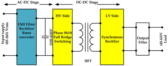
Figure 1.
Block diagram of the complete AC–DC power supply for a telecom server.
The design of power supply with a high input power factor requires the modifying of the input AC current waveform to follow the input voltage waveform to reduce the phase shaft between them, and then the reduction of the harmonic contents of the input current [3]. The power supply first stage usually includes an electromagnetic interference (EMI) filter, bridge rectifying circuit, boost converter, and output bulk capacitor; by controlling the boost converter operation, the input power factor can approach to, or near to, unity [4]. Single switch, two switches or full bridge switching topology can be used to implement PFC boost converter, but switching topology proper switches must be used to withstand the output voltage stress of this stage normally (320–400 V) DC [1]. Different techniques and topologies of the analog control PFC stage of the telecom power supply with power factor more than 99% are previously discussed in [5].
The power supply second stage is the target of this paper and it is designed to regulate the PFC output voltage to the required load voltage (usually 45–63 V) for the telecom applications. In this stage we must choose an appropriate technique to provide high power density conversion with high efficiency [6], DC–DC converter based on phase shifted ZVS technique is one of the most widely used techniques, because it has features to minimize the switching losses and offer better regulation over a wide load range [7]. Moreover, by using the ZVS technique, it is available to have high power density conversion with low voltage stress and small switching losses [8,9,10].
Switches on both sides of the high power density DC–DC converter must be designed to withstand the high voltage stress in the primary side and the high current stress in the secondary side [10]. So, one of the most important issue in designing DC–DC converter circuits is to choose the appropriate switching schematics for the converter to reduce the stress in the switches during the converter operation. Based on the phase shifted converter applications, phase shift pulse width modulation (PWM) converter can be implemented using different switching schematics (full bridge, half bridge, dual half bridge) in primary and secondary sides, and analysis of phase shifts isolated DC–DC converter different topologies previously given in [11]. Analysis and design of phase shift controller for a dual half bridge DC–DC converter is provided in [12]. Based on the application of DC–DC converter, it can be designed as an isolated or non-isolated converter; for the isolated DC–DC converter, transformer design and choice are a big challenge to have ZVS for the wide range of the load, which can reduce the switching and conduction losses [13]. Analysis of the phase shifted converter by using series connected transformers for low conduction losses are given in [14,15]. Design and implementation of the non-isolated phase shift ZVS converter is presented in [16].
DC–DC converter control circuits can be implemented using analog or digital control circuits, but analog control chip as compared with digital micro controller unit (MCU) has some demerits such as the temperature drift, fixed control parameters, and slow response speed; on the other hand the price of the MCU and the required analog digital interfacing sensors are expensive as compared with the analog control technique requirement. Optimization analysis and the design of different control techniques for the DC–DC converter have been previously presented in [17,18,19,20,21]. Design of 1 kW efficient phase shift telecom DC–DC converter based on the maximum duty cycle and optimal hold-up time is given in [22]. Controlling techniques to reduce the switching and conduction loss are presented in [23,24].
The bulk capacitor, which is introduced between the two stages of power supply as shown in Figure 1 for adjustment of the input voltage hold-up time and harmonic values of the input waveform, causes high inrush current for a few cycles where a very high “dv/dt” occurred at the initial power application to the power supply; this high dv/dt cause spikes of short-duration and a high peak current, which value may be higher than the circuit component rating current and can seriously damage or destroy these components [25,26,27]. So appropriate inrush current controlling circuit must be designed to limit such this current. Usually, limiting and reducing of the high inrush current is done by using a large size inductor or resistors in series with the input capacitors [28], but by using these techniques, converter compact design, and weight and power losses cannot be optimally utilized.
In order to reduce the power dissipation on the series resistor, a parallel semiconductor switch or relay can be connected through the resistance. However, based on the converter operating current, size of the relay can be also excessive large. Moreover, by using of a semiconductor switch an appropriate controlling circuit must be designed to control the switch operation. Another technique used to control the inrush current is by handling a soft starter time at the beginning of the DC–DC converter operation; soft starter technique works to limit inrush current based on controlling the duty cycle of the converter switches in order to slowly charge the capacitors, and hence reduce the high dv/dt for limiting the inrush current [29,30,31]; this technique is usually implemented to limit the inrush current inside the analog controller chips such as PWM controller integrated circuits (IC’s) UCC256403 and UCC28950 from Texas Instruments, Dallas, Texas, United States, 2016 [32].
Recently, NTC thermistor is the most famous device used in reducing the inrush current generated in the telecom power supplies. An NTC thermistor has a compact size and a negative temperature coefficient, is connected in series with the input power supply, and when the current flows, its temperature will increase and the device resistance will decrease [33,34]. The shortcoming of this device is that it requires a cool off time after the stopping of the current flowing in order to return back the device high resistance.
Another more applicable and simple technique to limit the converter inrush current can be done using a single MOSFET switch connected with the input side of the DC–DC converter [35,36,37]. MOSFETs switches are usually considered as ideal devices because they are characterized by fast switching time due to majority carrier, lower switching losses due to fast rise and fall times, as well as very small on-state DC resistance, which helps to reduce the voltage drop through the switch at steady state operation [38]. Control of the inrush current to the required limit can be done by controlling the gate charge transfer characteristics of the MOSFET switch in order to control the slew rate of the input capacitance charging time [39]. This technique offers inrush current control with economic price, compact design, and simple implementation, without using any sophisticated control circuit for the MOSFET operation [38,39,40]. High reliability using this technique can be obtained with the appropriate choice of the MOSFET switch, as well as design of the biasing circuit schematic and the connection strategy to the input side of the DC–DC converter [41].
In this paper, complete design, analysis, and mathematical calculations of the circuit main components and control systems of 2 kW, 54 V telecom DC–DC converter stage with phase shift ZVS technique, using full bridge at primary and synchronous rectification at secondary side are presented. A sample inrush current controlling circuit based on using MOSFET switch is proposed and is inserted in the input side of the DC–DC converter, proposed controlling circuit schematics as well as design and choice of the circuit components are briefly discussed. The main advantages of the proposed circuit are that the controlling of the gate charge transfer characteristics of the MOSFET occurs without any contribution or connection with the DC–DC converter control circuit, which make the proposed circuit usable with analog and digital control converters, and has fast response and high reliability to control the inrush current to the required value as well as simple implementation for any converter with different input–output operation conditions. The designed main components and control system of the power supply circuit make the power supply output voltage performance follows the standard specifications IEC61000-3-3, which is required by telecom applications.
The result sections of this paper are organized as follow: first, simulation of the complete designed converter is performed using PSIM software to be sure that the reliability of the designed components enhances the required power supply performance. Then, an experimental setup of the designed converter with the proposed inrush current mitigation circuit is inserted between the power supply two stages is performed in the lab, which shows that the designed DC–DC converter with proposed inrush control circuit can achieve smooth startup operation at the input side, where efficiency is more than 95.5%, and with better voltage regulation at the output side of the converter.
2. Design Procedure of the DC–DC Stage of the Telecom Power Supply
Figure 2 shows the schematic circuit of the telecom DC–DC converter stage with the proposed inrush current control circuit connected at the input side of the DC–DC phase shift converter. In designing the high-power density power supply with high conversion efficiency, losses in this stage must be maintained at their lowest value; one of the highest efficiency conversion techniques at high power density is the full bridge phase shift converter, which can offer very small switching losses by means of the ZVS technique at the converter primary side, which leads to increase the conversion efficiency [7,42].
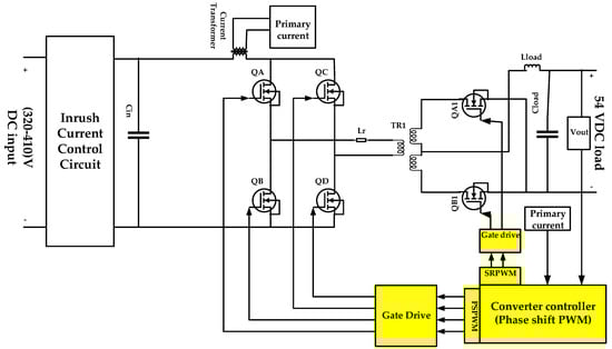
Figure 2.
Schematic diagram of DC–DC phase shift ZVS converter with the proposed inrush current control.
The most important components in the DC–DC converter stage to be designed in the next subsections are the input filter capacitor (Cin), inrush current control circuit, resonant inductor (Lr), transformer (TR1) turns ratio (a) and magnetizing reactance (Lm), and load inductance and capacitance (Lload and Cload). Other important factors are the choice of appropriate switches for the full bridge rectifier at the primary side and synchronous rectifier at the secondary side, which can withstand the high voltage stress at transformer primary and high current rated at secondary side [42].
2.1. Input Capacitor Design
Input capacitor of the DC–DC converter is designed to meet the hold-up time (thold) for the minimum input voltage (Vin min) applied to the converter circuit [15,40], and can be calculated as
where Po refers to the rated converter power, Vin refers to the Converter input voltage, and η is the designed efficiency of the DC–DC converter.
2.2. Proposed Inrush Current Control Circuit
In this subsection the proposed inrush current control circuit based on the controlling of the gate charge characteristic of the MOSFET switch was designed to be used with any DC–DC converter topology (analog or digital); the proposed circuit was tested in PSIM software and also was implemented in the lab to show the power supply two stages (PFC and DC–DC converter) practical current characteristic with, and without, using this circuit.
The input of DC–DC converter stage usually contains filter to adjust the total harmonics distortion (THD) of the input voltage to the DC–DC converter. Input filters usually consist of passive elements such as capacitor and inductor; when power is initially applied to the DC–DC converter circuit, high inrush current will flow due to high dv/dt of the filter capacitor as illustrated in Figure 3, which shows the converter input current curves at initial power application to the converter circuit.
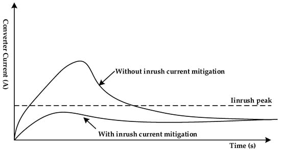
Figure 3.
Inrush current at the startup operation of DC–DC converter.
Mathematical analysis, which briefly describes the startup response of the power supply operation and the phenomena of the inrush currents in DC–DC converters, are previously discussed in [26,27]. At the moment of applying the voltage to the DC–DC converter circuit, the current flowing through the input capacitor (Cin) can be expressed as
This current has a high amplitude with very small duration and can damage or destroy circuit components if it exceeding the rating of the designed components. Therefore, this current must be effectively managed to ensure system safety operation and stability.
MOSFET switches are charge controlled devices, so if a MOSFET device is connected between two stages of the power supply, as shown in Figure 4, inrush current due to high dVin/dt, which is caused by the input capacitor (Cin) at the initial power application, can be controlled by controlling the initially high dVin/dt of the input capacitor by using the ability to control the constant linear slope of the drain voltage transition, which allows accurate control of the inrush current to the capacitive load. This is possible because the current flowing through the capacitor is dependent upon the transition of the voltage as shown in Equation (2). Reliability of this technique depends on the ability to control the MOSFET gate charge transfer curve illustrated in Figure 5 [29].
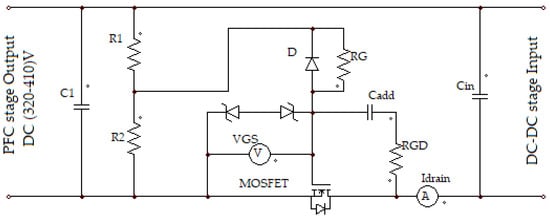
Figure 4.
Proposed inrush current controlling circuit.
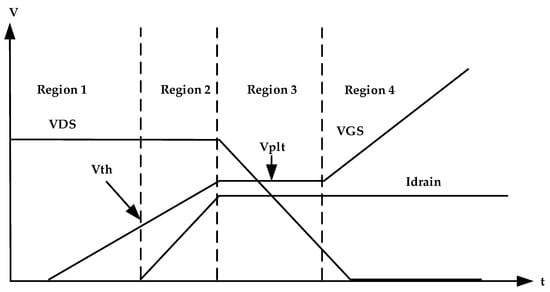
Figure 5.
Gate charge transfer characteristics of MOSFET.
Figure 6 shows the equivalent representation of the MOSFET switch, where the gate charge curve is influenced by the MOSFET equivalent input capacitance [29].
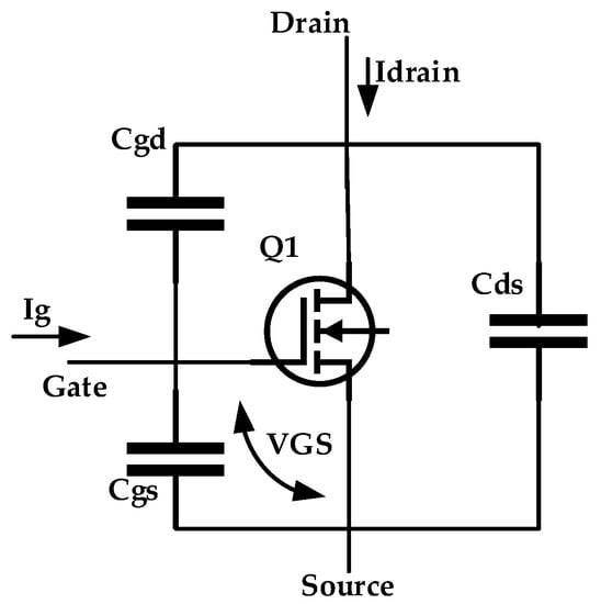
Figure 6.
Circuit of N-MOSFET.
Cgd and Cgs represents the gate-drain and gate-source capacitances, respectively; these two capacitance values represent the input capacitance of the MOSFET device. Usually for MOSFET, Cgd is greater than Cgs. So Cgd strongly influences the input capacitance of the MOSFET, this means that MOSFET input capacitance can control the inrush current value, if the value of Cgd is controlled. By inserting the appropriate design capacitance, Cadd, between the drain and gate terminals of MOSFET, as shown in the proposed circuit in Figure 4, Cgd can be controlled, which then can control the slew rate of the gate-source voltage, VGS, which controls the slew rate of the input capacitance charging (dVin/dt), and consequently controls the inrush current of the circuit.
As shown in the characteristics in Figure 5, when MOSFET is turned on, the charging of the equivalent capacitance occurs at Region 1, and the charging time is determined by the equivalent input capacitance of MOSFET. The voltage (VGS) increases until the starting point of Region 2, where it reaches the threshold value (Vth). At this time drain current starts to flow and the rate of increase of drain current given by
where gf is the switch forward trans-conductance and can be easily know from the switch datasheet.
At the end of Region 2, charging and discharging of Cgs simultaneously occurs, which causes VGS to be maintained constant at Miller plat voltage (Vplt) as shown in Region 3. With Vplt, the drain current is saturated at peak constant value dependent of VGS voltage value, and Vplt can be calculated as
The constant voltage of VGS causes the input gate current to flow through the additional capacitance Cadd, and can be calculated as
where RG is designed and connected in a series with the gate for controlling the gate current Ig. Finally, by controlling the value of VGS and Ig, it is possible to control the maximum drain current of the MOSFET and control the inrush current at the initial power application to the power supply circuit, when the drain terminal of the MOSFET is connected to the return path of the DC–DC converter, as shown in Figure 4. RGD, a small value resistor, as compared with RG, connected with the Cadd and prevents unwanted high frequency oscillation [29]. Using Equations (5) and (6) inrush peak current value is approximately given by
The value of this current must be less than the maximum permissible DC current (inrush peak) of the primary side of the DC–DC converter stage.
Figure 7 shows the flow chart for the complete design procedure for the proposed inrush current control circuit by using the method of the controlling in the gate charge transfer characteristics of the MOSFET.
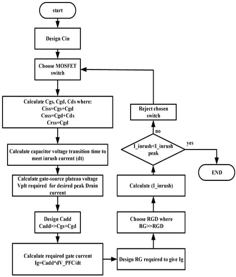
Figure 7.
Flow chart of design process of the proposed inrush current control circuit.
In Region 4, VGS still increases to higher values. If this voltage reaches a value higher than the gate source breakdown voltage (BVGS), MOSFET may be damaged; therefore, MOSFET must be protected at this region from the higher applied voltage; therefore, PFC output stage voltage (input voltage to the DC–DC converter) is divided using resistors R1 and R2 and only a small voltage is required to be applied to the MOSFET. Additionally, we can use one switch from the family of Zener-protected MOSFETs, such as switches from STMicroelectronics company [43]; in this protected switch, when the voltage applied to the switch is more than the breakdown voltage of the Zener (less than BVGS), the Zener diode breaks down and the voltage is saturated at the safe limit. The design result of the active inrush current control circuit, which used in simulation and experimental modeling is shown in Table 1.

Table 1.
Design Results for Active Inrush Current Control Circuit.
2.3. Transformer (TR1) Turns Ratio (a) and Magentizing Reactance (Lm) Calculation
Transformer turns ratio (a) is calculated based on maximum operating duty cycle (Dmax) at the minimum input voltage rating of the converter (Vin min) as follows:
Let Dmax be about 70% and Vin min about 320 V, and the transformer turns ratio is calculated as
where VDQ is the switch voltage drop and it is assumed to be 0.5 V in calculations.
Let a = 5, the typical operating duty cycle (D), is calculated as
Transformer magnetizing inductance (Lm) designed based on the maximum magnetizing inductance to realize ZVS as expressed in [13,18], and can be expressed as
where CHB refers to the total equivalent capacitance of the primary H bridge, which can be known from the primary switch data sheet. Ts min is the minimum switching time depends on the designed minimum switching frequency, also Tdead is the PWM dead time which can be calculated according to the previously calculated duty ratio.
One more important issue is the choosing of a transformer with appropriate magnetizing inductance to minimize the output current ripple and to make sure that the converter works in the required control mode, where the smallest value of magnetizing inductance makes the converter work in voltage control mode instead of current control mode [10].
2.4. Resonant Inductor (Lr) Design
Resonant inductor tank is calculated based on the amount of energy required to achieve ZVS condition. The energy absorbed by the inductor values of the resonant inductance (Lr) and the transformer leakage inductance (Llk) must be able to exhaust the energy supplied by the average parasitic capacitance of the primary switches (Cossavg), and also the energy from the transformer winding capacitance (Cw) [42,44].
where IP refers to the converter primary current (A).
2.5. Output Inductance and Capacitance (Lload and Cload)
Output load inductor (Lload) is designed based on 10% ripple value in the load DC current (Iload), as follows:
Output load capacitor (Cload) is selected based on hold-up time (thu) and 20% (200 mV) of the allowable load transient voltage (Vtran) as follow:
where hold-up time (thu) is calculated as the time required for the inductor current to reach to 90% of the full load current [41].
2.6. DC–DC Converter Controller Design and Implmentation
Phase shift PWM technique is used to control the full-bridge in the primary side of the DC–DC converter by phase shifting the switching pulses of one half-bridge with respect to the other. High power density efficient conversion is available using ZVS technique at high switching frequency in this part. Voltage-mode or current-mode control techniques can be used in this part. Current-mode controlled DC–DC switching is popular and provides a more highly efficient power conversion than voltage mode control. However, the current-mode design can suffer from instability when the duty cycle of the PWM rises above 50% [45]. To overcome this instability, converter primary current slope compensation technique is used to restore reliability over the wide range of duty-cycle [19,46].
Figure 8 shows the schematic of control technique of DC–DC converter, implemented in PSIM software where the primary current and the output voltage are the feedback signals used in this control system. First, primary current is sensed using current transformer with turns ratio (100:1) and then sampled by a resistor to get a primary current signal (VIp); load voltage (Vload) signal is also sensed. To overcome the instability in current waveforms at high duty cycles, value slope compensation technique with the ramp signal of 200 kHz is added to the VIp signal to generate the primary current (Iprim); output DC voltage signal is compared with the appropriate reference value and passed to the voltage PI controller to generate the primary current reference value (Iprim-ref), then the primary current (Iprim) is compared with reference value (Iprim-ref) to generate the duty cycle of the PWM generator for the primary and secondary switches QA, QB, QC, QD, QA1, and QB1.
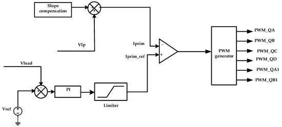
Figure 8.
Technique of the phase shift PWM DC–DC converter controller.
Table 2 shows the input/output specifications and the results of the design converter main components of the DC–DC converter.
Table 2.
DC–DC Converter Specifications and Design Results.
3. Simulation Results and Discussions
Phase shift DC–DC converter with power density about 2 kW has been implemented in PSIM software using the designed components in the previous sections to show the system performance under different loading conditions and to test the reliability of inrush controlling circuit to limit the high inrush current at initial power application to the primary side of the power supply circuit.
With full load condition and DC input voltage about 400 V, Figure 9 shows the steady state simulation result of the DC output power curve of the DC–DC converter.
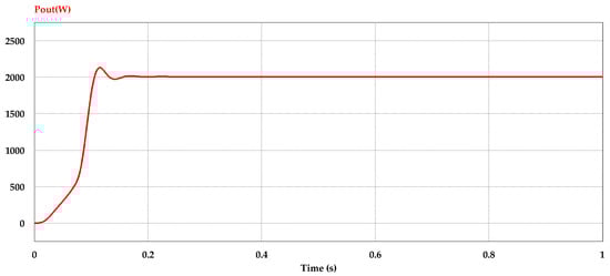
Figure 9.
Converter output power curve at full load condition.
The designed power supply efficiency curve at loading condition from 10% to 100% of the rated output power (2 kW) with input voltage 400 V and switching frequency about 100 kHz is illustrated in Figure 10, which shows that the designed power supply offers full-load efficiency at about 95.1%, half-load efficiency at about 95.3%, and the maximum being three-quarter-load efficiency at about 95.6%.

Figure 10.
Converter efficiency curve with different loading condition at Vin = 400 V.
As mentioned before in Section 2.2, the gate charge transfer characteristics of the MOSFET switch can be used to control the slew rate of the input capacitance charging in order to control and limit the inrush current to the required value. Figure 11 shows the bulk input capacitance charging voltage curves with, and without, using the proposed inrush current control circuit, where the black curve refers to the supply DC input voltage, the red curve is the voltage curve of the input capacitance without using the proposed control circuit, and the blue curve is the voltage curve of the input capacitance using the proposed control circuit. From these curves, it is clearly observed that controlling the slew rate of VGS voltage by controlling the input capacitance of the MOSFET, leads to the reduction of the high dv/dt of the input capacitance, which subsequently reduces the inrush current at initial power application.
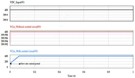
Figure 11.
Bulk input capacitance charging voltage with and without using the proposed control.
Waveforms of the average value of the converter input current at switching frequency of 100 kHz with, and without, using the inrush current control circuit are shown in Figure 12 and Figure 13, respectively. From both cases, and as the result of controlling the voltage slew rate at the initial power application to the converter circuit based on the transition time, which is required to meet the required inrush current, we can notice that the proposed controlling circuit reduced the peak inrush current from 16.10 A to about 6.40 A, which is in the allowable range (given in Table 1) of the input DC current to the primary side of DC–DC converter; moreover, it is clear to observe that the peak value of the input current at steady state with full load condition is about 8.20 A in both cases.
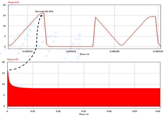
Figure 12.
Converter input current without inrush current mitigation circuit at full load and Vin = 400 V.
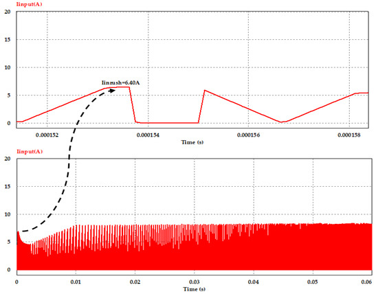
Figure 13.
Converter input current with inrush current control circuit at full load and Vin = 400 V.
Figure 14 shows the VGS and Idrain characteristics of the MOSFET in the inrush current control circuit. When the VGS voltage reached to Vth (about 3.75 V) of the used MOSFET switch, the drain current starts to increase, at the point when VGS reaches Vplt, and circuit inrush current tries to increase but based on the gate charge transfer characteristic depicted in Figure 5, drain current saturated at constant value about 6.40 A as shown in the simulation result. Additionally, from this figure it is clearly observed that the protection of the MOSFET switch, which occurred at Region 4 when the Zener diode circuit broke down before the voltage reached 30 V (BVGS of the used MOSFET) and the voltage was saturated at about 28.5 V.
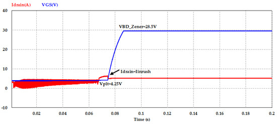
Figure 14.
Gate charge waveform of the MOSFET in inrush current mitigation circuit.
Phase shift PWM controlling circuit and the resonant inductor are designed to offer ZVS at the two legs of the bridge at the primary side of the DC–DC converter switches, as shown in current and voltage waveforms of the switches (QA and QC) in Figure 15 and Figure 16.
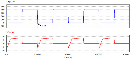
Figure 15.
Voltage and current waveforms of switch QA converter primary side at Po = 2 kW.
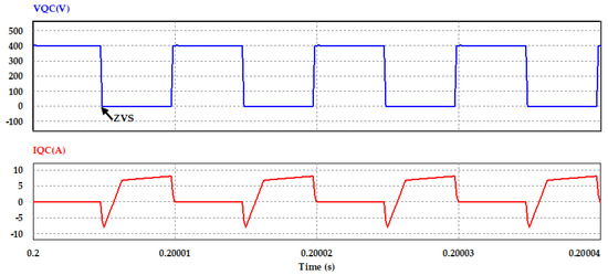
Figure 16.
Voltage and current waveforms of switch QC in converter primary side at Po = 2 kW.
4. Experimental Setup
The complete designed converter circuit and the proposed inrush current mitigation circuit are experimentally setup and tested with the available maximum DC electronic load in the lab (1000 W), UCC28950 phase shift PWM controller IC from Texas Instruments, Dallas, Texas, United States, 2016 is used to control the DC–DC converter switches, UCC28950 IC provide 4-PWM signals with constant frequency (100 kHz) for the primary side switches, and 2-PWM for the synchronous rectification at the secondary side switches with the availability of the primary current compensation to restore the current stability and the voltage loop control to adjust the output voltage at the specified value.
The proposed inrush current mitigation circuit was tested with the practical case of the telecom two stages AC–DC power supply, where the DC–DC converter was supplied by the PFC converter stage with output voltage of 400 V DC. In order to show the reliability of the proposed inrush current control circuit in mitigation of the high current overshot in the input current to the converter, soft starter of the analog UCC28950 IC is disabled through the (SS/EN) pin and only the proposed inrush current control circuit is connected to the input side of the DC–DC converter circuit.
Figure 17 shows the appearance of the experimental setup of the complete power supply consisting of PFC and DC–DC converter stages and with using the proposed inrush current control circuit connecting in between. 1000W KIKUSI PLZ1004WH, Japan, 2019 DC electronic load was connected at load side, and 2.5 kW PFC converter stage from Infineon with average efficiency more than 95% [47], inrush current control circuit was connected between the two stages and the input AC voltage was applied to the input of the PFC stage so that the output voltage will be 400 V DC, input current to the both stages has been measured using high scale current probe FLUKE i1000s, USA, FLUKE company with scale choice of (10:1) A with, and without, connecting of the proposed inrush current mitigation circuit.
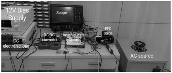
Figure 17.
Experimental setup of DC–DC converter circuit with inrush current mitigation circuit.
Figure 18 and Figure 19 show the DC–DC converter stage input current, from which we can investigated that with using inrush current control circuit, the inrush current at the startup of the converter is reduced from 20.32 A to about 4.06 A. Additionally, in both figures, differences in current shape and starting time of each waveform can be observed, this occurred due to changing in the slew rate of the input capacitance voltage, which leads to limit the inrush current at the safe limit using the inrush current controlling circuit, in Figure 19, with the current still increasing gradually until it reached to 4.06 A, at this moment, and as explained before in the controlling circuit characteristics in Figure 14, the drain current is saturated at the safe limit to prevent the inrush current from increasing to higher limits.
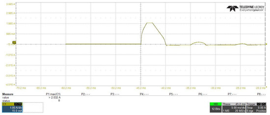
Figure 18.
DC–DC converter stage input current without using of the proposed inrush current mitigation circuit.
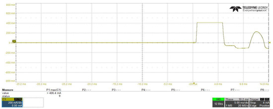
Figure 19.
DC–DC converter stage input current with using of the proposed inrush current mitigation circuit.
Figure 20 and Figure 21 show the PFC converter stage AC input current, from which we can investigate that by connecting the proposed inrush current control circuit between the two stages of the power supply, the peak overshoot of the input current to the PFC stage will reduced from 33.55 A to 15.33 A. Additionally, the difference is noticed between starting time and waveform shapes, due to the controlling of the slew rate of the input voltage by using the proposed inrush current control circuit.
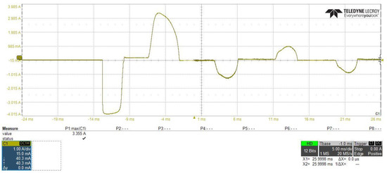
Figure 20.
Power factor correction (PFC) converter stage AC input current without using of the proposed inrush current mitigation circuit.
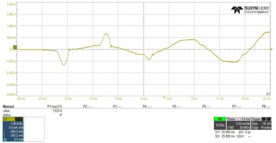
Figure 21.
PFC converter stage AC input current with using of the proposed inrush current mitigation circuit.
Figure 22 shows the converter output voltage and current waveforms at steady state operation using the inrush current control circuit, in which the converter DC output power was about 1085.25 W, where the output voltage was constant at about 54.02 V and current value was about 20.090 A.
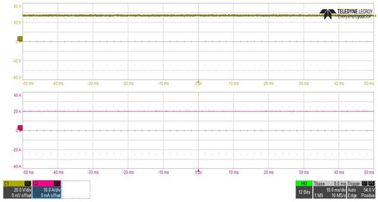
Figure 22.
DC–DC converter stage output voltage and current waveforms at Vin = 400 V.
DC–DC converter output filter capacitor was designed to maintain the output voltage ripple to the specified value as explained previously in Section 3; in order to clearly observe the ripple component in the output voltage waveform, the vertical axis scale of the voltage was changed and the measurement set in scope was adjusted to measure the ripple peak to peak value and the mean value of the voltage waveform, as shown in Figure 23, which clearly shows that the peak to peak ripple voltage is about 34.4 mV (less than the designed value 200 mV) and the mean output voltage value is about 54.094 V.
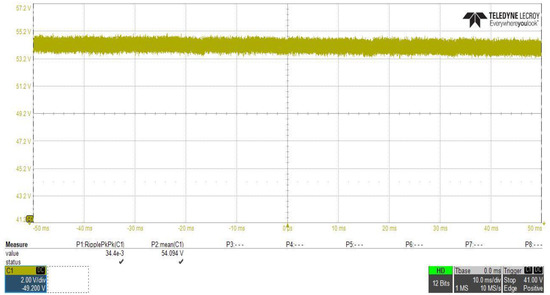
Figure 23.
DC–DC converter stage output voltage ripple peak to peak measurement at Vin = 400 V.
In case of designing the DC–DC converter stage for the telecom applications, voltage controller must be implemented in order to achieve different loading condition with good voltage regulation. Figure 24 depicts the output voltage versus output power, which shows that the designed DC–DC converter with the proposed inrush current controlling circuit also provides different loading conditions with good voltage regulation, where the voltage drop is less than 1 V (1.85%) for changing loading conditions from 200 W to 1000 W, which is less than the IEC61000-3-3 standard limit for the limitation of the voltage changes (3.3%) [48].
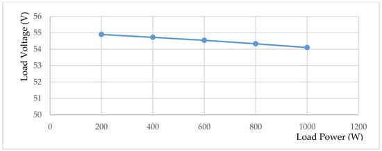
Figure 24.
DC–DC converter load voltage-power characteristics at Vin = 400 V.
The inrush current control circuit, designed and connected between the two stages of the power supply, to control the inrush current at the initial power application to the power supply, must not effect the performance of the PFC stage at steady state operation. To study the effect of the proposed inrush current control circuit on the PFC converter performance, power analysis of the input side of the PFC converter have been performed with, and without, using the inrush current control circuit with the same loading and input voltage conditions as shown in Figure 25 and Figure 26, which clearly shows that the reduction in the inrush current of the input supply at initial power application leads to a reduction in the supply total reactive power from 103 VA to about 90 VA, and it can also clearly be observed that the power factor value of the power supply was not affected by the connection of the proposed circuit.
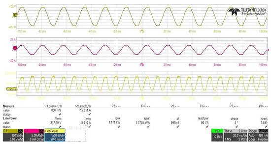
Figure 25.
PFC converter stage power analysis with using of the proposed inrush current mitigation circuit.
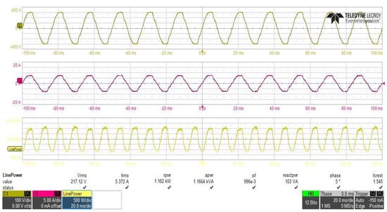
Figure 26.
PFC converter stage power analysis without using of the proposed inrush current mitigation circuit.
As shown in Figure 22 the total input power to the two stages with inrush current control circuit is about 1171 W, and as shown in Figure 25, the load power is about 1085.25 W, so the power supply includes about 85.75 W power losses, distributed as 39.5 W in the PFC stage with efficiency of about 96.62% and 46.25 W in DC–DC converter and inrush current control circuit, with efficiency of about 95.73%, which is very close to the simulation results (95.40%) at the same loading. Total losses distribution in the system different parts are performed and the result is depicted in Figure 27.
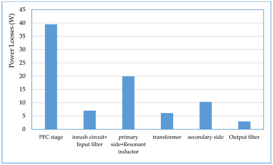
Figure 27.
Losses distribution in different parts of the two stages power supply with inrush current control.
From the loss distribution of the power supply, it is noticed that the highest budget of the DC–DC converter losses was accounted by the primary side bridge and the resonant inductor with about 20 W; this loss amount is due to primary side switches internal resistance and forward voltage drop, and also due to the internal DC resistance of the resonant inductor. The second highest budget of the power losses accounted in the secondary side synchronous switches with about 10.5 W. Power loss of about 6 W was dissipated in the converter transformer primary and secondary DC resistances. Internal DC resistance of the output filter inductor and the equivalent series resistance (ESR) of the output electrolytic capacitor introduce power loss about 3 W. The remaining converter power losses budget was accounted by the proposed inrush current control circuit and the ESR of the bulk input electrolytic capacitor. One disadvantage of the proposed inrush current, is that it has an amount of about 5 W of the total supply power losses, but on the other hand, it has many advantages, which can be summarized in the following:
- Compact design and easy implementation with cheap passive elements and single MOSFET.
- Controllability and reliability of the circuit to limit the inrush current at the required value.
- Reduce the current stress on the input side of the two stages of power supply at initial power application.
- Improve the PFC stage performance by reducing the total reactive power consumption of the circuit.
- Easy to disconnect and reconnect again between two stages of a faulty case as compared with the IC soft starter (in case where the IC soft starter function is damaged).
- Ability to use with analog and digital control converter.
5. Conclusions
Complete design of a high power density efficient DC–DC converter stage of the telecom power supply has been discussed in this paper; a high inrush current, which is generated between two stages of power supply where the bulk input capacitor is controlled using the proposed simple inrush current control circuit designed by using single MOSFET switch and some passive elements. Simulation analysis as well as experimental setup of the practical two stages telecom power supply and inrush current control circuit is performed. Phase shifted PWM with ZVS technique is applied in DC–DC converter stage, which provided system experimentally overall efficiency about 95.73% at 50% loading condition. Furthermore, reliability of the converter designed components to achieve the performance of the telecom power supply was established; ability of the proposed inrush current control circuit to control the slew rate of the input capacitance voltage in order to reduce the high dv/dt and to mitigate the inrush current of the input current of the two stages of power supply was also achieved, which ensures a safe and smooth startup operation of the power supply.
Author Contributions
The literature review and manuscript preparation, as well as the simulations, were carried out by A.H.O. Experimental results and implementation of the prototype were carried by A.H.O. and J.B. Final review of manuscript corrections was done by N.K. and J.B. All authors have read and agreed to the published version of the manuscript.
Funding
This research was funded by grant (2018R1D1A3B0704376413) from National Research Foundation of Korea (NRF) and grant (18RTRP-B146050-01) from Railroad Technology Research Program (RTRP) funded by Ministry of Land, Infrastructure and Transport of Korean government.
Conflicts of Interest
The authors declare no conflict of interest.
References
- Garcia, O.; Cobos, J.A.; Prieto, R.; Alou, P.; Uceda, J. Single phase power factor correction: A survey. IEEE Trans. Power Electron. 2003, 18, 749–755. [Google Scholar] [CrossRef]
- Geddam, D.P.; Prakash, D.; Bapu, S.R.; Kumar, Y.R.; Rao, P.S.; Naidu, G.K.M.; Ramanarayanan, V. Design of 1.4 kw telecom rectifier delivering full power from 90Vac to 300Vac. In Proceedings of the IEEE INTELEC 07–29th International Telecommunications Energy Conference, Rome, Italy, 30 September–4 October 2007; pp. 670–676. [Google Scholar]
- Kasper, M.; Bortis, D.; Deboy, G.; Kolar, J.W. Design of a Highly Efficient (97.7%) and Very Compact (2.2 kW/dm3) Isolated AC–DC Telecom Power Supply Module Based on the Multicell ISOP Converter Approach. IEEE Trans. Power Electron. 2016, 32, 7750–7769. [Google Scholar] [CrossRef]
- Sekar, A.; Raghavan, D. Implementation of single phase soft switched PFC converter for plug-in-hybrid electric vehicles. Energies 2015, 8, 13096–13111. [Google Scholar] [CrossRef]
- Kim, Y.-S.; Sung, W.; Lee, B. Comparative performance analysis of high density and efficiency PFC topologies. IEEE Trans. Power Electron. 2003, 6, 2666–2679. [Google Scholar] [CrossRef]
- Biela, J.; Badstuebner, U.; Kolar, J.W. Impact of power density maximization on efficiency of DC–DC converter systems. IEEE Trans. Power Electron. 2009, 24, 288–300. [Google Scholar] [CrossRef]
- Yang, B.; Duarte, J.L.; Li, W.; Yin, K.; He, X.; Deng, Y. Phase-shifted full bridge converter featuring ZVS over the full load range. In Proceedings of the IECON 36th Annual Conference on IEEE Industrial Electronics Society, Glendale, AZ, USA, 7–10 November 2010; pp. 644–649. [Google Scholar]
- Lo, Y.-K.; Lin, C.-H.; Hsieh, M.-I.; Lin, C.-H. Phase-shifted full-bridge series-resonant DC–DC converters for wide load variations. IEEE Trans. Ind. Electron. 2010, 58, 2572–2575. [Google Scholar] [CrossRef]
- Schmidt, J.C.M.; Maragaño, J.C.; Sartori, H.C.; Pinheiro, J.R. Design methodology to achieve high-efficiency isolated ZVS DC/DC converters. In Proceedings of the 2017 IEEE 8th International Symposium on Power Electronics for Distributed Generation Systems (PEDG), Florianopolis, Brazil, 17–20 April 2017; pp. 1–8. [Google Scholar]
- Badstuebner, U.; Biela, J.; Kolar, W.J. Design of an 99%-efficient, 5kW, phase-shift PWM DC–DC converter for telecom applications. In Proceedings of the 2010 Twenty-Fifth Annual IEEE Applied Power Electronics Conference and Exposition (APEC), Palm Springs, CA, USA, 21–25 February 2010; pp. 773–780. [Google Scholar]
- Bai, H.; Nie, Z.; Mi, C.C. Experimental comparison of traditional phase-shift, dual-phase-shift, and model-based control of isolated bidirectional DC–DC converters. IEEE Trans. Power Electron. 2009, 25, 1444–1449. [Google Scholar] [CrossRef]
- Xiangli, K.; Li, S.; Smedley, K.M. Decoupled PWM plus phase-shift control for a dual-half-bridge bidirectional DC–DC converter. IEEE Trans. Power Electron. 2017, 33, 7203–7213. [Google Scholar] [CrossRef]
- Hurley, W.G.; Wölfle, W.H. Transformers and Inductors for Power Electronics. Theory, Design and Applications; Wiley: London, UK, 2013. [Google Scholar]
- Koo, G.B.; Moon, G.W.; Youn, M.J. New zero-voltage-switching phase-shift full-bridge converter with low conduction losses. IEEE Trans. Power Electron. 2005, 52, 228–235. [Google Scholar] [CrossRef]
- Kathiresan, R.; Das, P.; Reindl, T.; Panda, S.K. A novel ZVS DC–DC full-bridge converter with hold-up time operation. IEEE Trans. Ind. Electron. 2017, 64, 4491–4500. [Google Scholar] [CrossRef]
- Das, P.; Laan, B.; Mousavi, S.A.; Moschopoulos, G. A non-isolated bidirectional ZVS-PWM active clamped DC–DC converter. IEEE Trans. Power Electron. 2009, 24, 553–558. [Google Scholar] [CrossRef]
- Bojoi, R.; Fusillo, F.; Raciti, A.; Musumeci, S.; Scrimizzi, F.; Rizzo, S. Full-Bridge DC–DC Power Converter for Telecom applications with Advanced Trench Gate MOSFETs. In Proceedings of the 2018 IEEE International Telecommunications Energy Conference (INTELEC), Lingnotto Fiere, Italy, 7–11 October 2018; pp. 1–7. [Google Scholar]
- Zhao, Z.; Xu, Q.; Dai, Y.; Yin, H. Analysis, Design, and Implementation of Improved LLC Resonant Transformer for Efficiency Enhancement. Energies 2018, 11, 3288. [Google Scholar] [CrossRef]
- Tao, H.; Zhang, G.; Zheng, Z.; Du, C. Design of Digital Control System for DC/DC Converter of On-Board Charger. J. Adv. Transp. 2019, 2019, 2467307. [Google Scholar] [CrossRef]
- Cho, J.-H.; Seong, H.-Y.; Jung, S.-H.; Park, J.-Y.; Moon, G.-U.; Youn, M.-Y. Implementation of digitally controlled phase shift full bridge converter for server power supply. In Proceedings of the 2010 IEEE Energy Conversion Congress and Exposition, Atlanta, GA, USA, 12–16 September 2010; pp. 802–809. [Google Scholar]
- Lee, Y.J.; Bak, Y.; Lee, K.Y. Control Method for Phase-Shift Full-Bridge Center-Tapped Converters Using a Hybrid Fuzzy Sliding Mode Controller. Electronics 2019, 8, 705. [Google Scholar] [CrossRef]
- Cho, I.-H.; Cho, K.-M.; Kim, J.-W.; Moon, G.-W. A new phase-shifted full-bridge converter with maximum duty operation for server power system. IEEE Trans. Power Electron. 2011, 26, 3491–3500. [Google Scholar] [CrossRef]
- Moisseev, S.; Soshin, K.; Sato, S.; Gamage, L.; Nakaoka, M. Novel soft-commutation DC–DC power converter with high-frequency transformer secondary side phase-shifted PWM active rectifier. IEE Electr. Power Appl. 2004, 151, 260–267. [Google Scholar] [CrossRef]
- Kim, Y.-D.; Cho, K.-M.; Kim, D.-Y.; Moon, G.-W. Wide-range ZVS phase-shift full-bridge converter with reduced conduction loss caused by circulating current. IEEE Trans. Power Electron. 2012, 28, 3308–3316. [Google Scholar] [CrossRef]
- Inrush Current in DC–DC Converters. Application Notes, vpt Power. Available online: http://www.vptpower.com/wp-content (accessed on 14 November 2019).
- Martínez-Salamero, L.; García, G.; Orellana, M.; Lahore, C.; Estibals, B. Start-up control and voltage regulation in a boost converter under sliding-mode operation. IEEE Trans. Ind. Electron. 2012, 60, 4637–4649. [Google Scholar] [CrossRef]
- Aroudi, A.E.; Martínez-Treviño, B.A.; Vidal-Idiarte, E.; Martínez-Salamero, L. Analysis of Start-Up Response in a Digitally Controlled Boost Converter with Constant Power Load and Mitigation of Inrush Current Problems. IEEE Trans. Circuits Syst. I 2019, 67, 1276–1285. [Google Scholar] [CrossRef]
- Mitter, S. Active Inrush Current Limiting Using MOSFETs; Motorola Inc.: Phoenix, AZ, USA, 1995; Available online: http://application-notes.digchip.com/010/10-13155.pdf (accessed on 10 January 2020).
- Kalenteridis; Vasileios; Agorastou, Z.; Siskos, S. A soft start-up technique for inrush current limitation in DC–DC converters. In Proceedings of the 2019 IEEE Panhellenic Conference on Electronics & Telecommunications (PACET), Volos, Greece, 8–9 November 2019; pp. 1–4. [Google Scholar]
- Ma, F.-F.; Chen, W.-Z.; Wu, J.-C. A monolithic current-mode buck converter with advanced control and protection circuits. IEEE Trans. Power Electron. 2007, 22, 1836–1846. [Google Scholar] [CrossRef]
- Sathishkumar, P.; Krishna, T.N.V.; Khan, M.A.; Zeb, K.; Kim, H. Digital soft start implementation for minimizing start up transients in high power DAB-IBDC converter. Energies 2018, 11, 956. [Google Scholar] [CrossRef]
- Managing Inrush Current. Application Report, Texas Instruments. Available online: http://www.ti.com/lit/an/slva670a/slva670a.pdf?&ts=1589053420769 (accessed on 12 January 2020).
- Jiang, T.; Cairoli, P.; Rodrigues, R.; Du, Y. Inrush current limiting for solid state devices using NTC resistor. In Proceedings of the IEEE Southeast Conference, Charlotte, NC, USA, 30 March–2 April 2017; pp. 1–7. [Google Scholar]
- NTC Thermistors Ordering Code. RS Components. Available online: https://docs.rs-online.com/ee83/0900766b80e7f61b.pdf (accessed on 12 January 2020).
- Dias, V.A.; Pomilio, J.A.; Finco, S. A current limiting switch for applications in space power systems. In Proceedings of the 2017 IEEE Southern Power Electronics Conference (SPEC), Puerto Valas, Chile, 4–7 December 2017; pp. 1–6. [Google Scholar]
- Fuengwarodsakul, N.H. Battery management system with active inrush current control for Li-ion battery in light electric vehicles. Electr. Eng. 2016, 98, 17–27. [Google Scholar] [CrossRef]
- Marroqui, D.; Garrigos, A.; Blanes, J.M.; Gutierrez, R. Photovoltaic-Driven SiC MOSFET Circuit Breaker with Latching and Current Limiting Capability. Energies 2019, 12, 4585. [Google Scholar] [CrossRef]
- Lee, E.-J.; Ahn, J.-H.; Shin, S.-M.; Lee, B.-K. Comparative analysis of active inrush current limiter for high-voltage DC power supply system. In Proceedings of the 2012 IEEE Vehicle Power and Propulsion Conference, Seoul, Korea, 9–12 October 2012; pp. 1256–1260. [Google Scholar]
- Musumeci, S. Gate charge control of high-voltage Silicon-Carbide (SiC) MOSFET in power converter applications. In Proceedings of the 2015 International Conference on Clean Electrical Power (ICCEP), Taormina, Italy, 16–18 June 2015; pp. 709–715. [Google Scholar]
- Manolarou, M.; Kostakis, G.; Manias, S.N. Inrush current limiting technique for low-voltage synchronous DC/DC converters. IEE Electr. Power Appl. 2005, 152, 1179–1183. [Google Scholar] [CrossRef]
- Manousaka, E. DC–DC Buck Converter with Inrush Current Limiter. Master’s Thesis, Faculty of Applied Sciences, Delft University of Technology, Delft, Wales, October 2013. [Google Scholar]
- UCC28950 600-W, Phase-Shifted, Full-Bridge Application Report. Texas Instruments. Available online: http://www.ti.com/lit/slua560 (accessed on 8 March 2020).
- N-CHANNEL 500 V –0.105Ω –31A TO-247 Zener-Protected MOSFET. Available online: https://www.st.com/resource/en/datasheet/cd00045267.pdf (accessed on 5 April 2020).
- “Power Electronics Handbook” Book; Available online: http://site.iugaza.edu.ps/malramlawi/files/RASHID_Power_Electronics_Handbook.pdf (accessed on 25 February 2020).
- Phase-Shifted Full-Bridge, Zero-Voltage Transition Design Considerations. Application Report. Available online: https://www.ti.com/lit/pdf/slua107 (accessed on 8 March 2020).
- Instruments Texas. Modeling, Analysis and Compensation of the Current-Mode Converter; Notes, Application; Texas Instruments Inc.: Dallas, TX, USA, 1999. [Google Scholar]
- 2.5kW PFC Evaluation Board with CCM PFC Controller ICE3PCS01G. Design Report, Infineon Company. Available online: https://www.infineon.com/cms/en/product/evaluation-boards/eval_2k5w_ccm_4p_v3/ (accessed on 15 April 2020).
- IEC/EN61000 Standards for Power Supplies. SL Power Application Note. Available online: https://slpower.com/App-slpower/images/whitepapers/AN-G007_EN61000.pdf (accessed on 12 August 2020).


© 2020 by the authors. Licensee MDPI, Basel, Switzerland. This article is an open access article distributed under the terms and conditions of the Creative Commons Attribution (CC BY) license (http://creativecommons.org/licenses/by/4.0/).