Abstract
In the permanent magnet synchronous generator (PMSG), the DC bus voltage fluctuates up and down under the influence of the load and power grid, which greatly affects the safe and reliable work of PMSG. In order to suppress the wide range fluctuation of DC bus voltage under disturbance and enhance its anti-disturbance performance, an optimized DC bus voltage control strategy is proposed by using the improved linear active disturbance rejection control (LADRC) in the voltage outer loop. By considering factors, such as load disturbance and grid voltage mutation as the total disturbance of the system, the improved reduced-order linear expansion state observer (RLSEO) is used to estimate and compensate the total disturbance, which greatly improves the stability of DC bus voltage. Firstly, the mathematical model of grid-side converter is established. On this basis, the LADRC control based on RLESO is designed, which reduces the phase lag of the linear extended state observer (LESO) and enhances the disturbance observation accuracy of the system. Then, a lead lag correction link is added to the total disturbance channel of RLESO to reduce the noise amplification effect of RLESO. Finally, the frequency domain characteristic analysis and stability proof of the improved LADRC control strategy are carried out. The simulation results show that the control strategy proposed in the article has a better control effect on the DC bus voltage.
1. Introduction
A permanent magnet synchronous generator (PMSG) has the characteristics of a simple structure, low maintenance cost, low noise, and flexible operation control, which has attracted more and more attention of researchers both domestic and foreign [1,2]. PMSG usually uses a dual pulse width modulation (PWM) converter to realize grid-connected power generation [3]. Its topology is shown in Figure 1. The motor-side converter is mainly responsible for controlling the output power of the PMSG, so as to make full use of wind energy [4]. The grid-side converter is mainly responsible for the safe and stable grid connection of the PMSG system, and realizes the stable control of the DC bus voltage [5]. For the grid-side converter, the conventional double closed-loop control strategy cannot achieve a satisfactory control effect [6]. When the working state of the motor or grid voltage changes suddenly, the DC bus voltage will rise sharply, resulting in the degradation of the PMSG system’s performance [7]. Therefore, adopting a more effective control strategy to suppress the DC bus voltage fluctuation is the key to ensure that PMSG has better performance indicators [8].
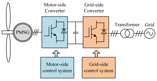
Figure 1.
Topological structure of the PMSG system.
At present, there are many control methods that can be used to enhance the transient performance of the DC bus voltage of the grid-side converter to resist sudden change of the grid voltage and load disturbance. In [9], the method of enlarging the capacitance of the DC bus can decrease the transient instability degree of the bus voltage, but this method not only increases the volume of the PMSG but also decreases the dynamic response of the system. In [10], the bus capacitance current is reconstructed by using the load information of the motor, which improves the anti-interference ability of the DC side voltage, but it is easily affected by the motor parameters and control strategies. the authors of [11] adopt master-slave control to ensure the power balance of the converters at both ends of DC bus. This modified method can enhance the stability of the DC link voltage in the case of a power network voltage disturbance. However, the control system of the grid-side converter and generator-side converter is coupled with each other, and the design of the system is complex. In [12], a direct control strategy of the DC link capacitance current is proposed. Based on the predictive effect of the differential, the DC link voltage can be tracked in real time more quickly, and the dynamic response of the system is enhanced. In [13], the control method of power feed-forward is adopted, and the active power is directly regulated by the current inner loop, which reduces the regulation time of the DC link voltage. However, when the motor load torque changes suddenly, its control effect on the DC link voltage is not obvious.
Active disturbance rejection control (ADRC) is a new control strategy proposed by Professor Han J.Q. It can make the internal and external disturbances, unmodeled dynamics, and other parts of the system equivalent, which are different from the integral series type into the total disturbance of the system [14], and the extended state observer (ESO) is used to estimate and compensate the total disturbance [15,16]. The authors of [17] apply ADRC to wind power inverters, which shows that it has a strong control effect for complex systems with strong coupling, both multivariable and nonlinear. The authors of [18] relate the controller parameters to the bandwidth and propose linear active disturbance rejection control (LADRC), which solves the problem of numerous parameters of traditional nonlinear ADRC. In [19,20], the known outputs of the system are deleted from the linear extended state observer (LESO), and an LADRC method based on the reduced-order linear extended state observer (RLESO) is proposed, which can reduce the phase lag of the system, and enhance the anti-interference rejection and robustness of the LADRC.
In this paper, the DC bus voltage is taken as the control object, and the LADRC control is constructed to replace the voltage outer loop. Because the DC bus voltage can be obtained by timely and accurate measurement in the measurement link, it is deleted from LESO, and a RLESO with the error of the DC bus voltage differential and its observed value as the feedback is constructed. By introducing the correction link based on the lead lag on the total disturbance channel, the amplitude attenuation of the RLESO is increased, and its noise amplification effect is weakened. Frequency domain analysis shows that the anti-disturbance performance of the modified LADRC is better than that of the traditional LADRC. The simulation verifies that the modified LADRC control strategy can ensure that the DC bus voltage has a better control effect under a low-voltage ride through (LVRT) faults.
2. Mathematical Model of the Grid-Side Converter
The topological structure of the grid-side converter is shown in Figure 2. Where ega, egb, and egc are the power network voltages; iga, igb, and igc are the power network currents; uga, ugb, and ugc are the phase voltages’ output by the grid-side inverter; Udc is the DC bus capacitor voltage; is is the load current; R is the power network-side equivalent resistance; L is the power network-side filter inductor; and C is the DC bus capacitance.
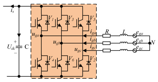
Figure 2.
Topological structure of the grid-side converter.
For the convenience of analysis, the following assumptions are made: The three-phase AC power supply of the grid is sinusoidal steady-state AC and three-phase symmetrical; the equivalent resistance and filter inductance of the power network side are all linear elements; and the switch is an ideal switch without conduction, shutdown delay, and loss. According to the structure shown in Figure 2 and Kirchhoff′s law, the following formula can be obtained:
where Sk represents the switching state of the switching device of the circuit bridge arm. When Sk = 1, it means that the switch of the upper bridge arm of the K phase is on; when Sk = 0, it means that the switch of the upper bridge arm of the K phase is off.
In Equation (1), although the physical meaning of the mathematical model is clear, since the parameters in the model are all sinusoidal time-varying parameters, this makes the design of the controller very difficult. Therefore, through park transformation, the mathematical model shown in Equation (1) is transformed into the d-q rotation coordinate system, which rotates synchronously with the fundamental voltage wave of the power grid, so as to realize decoupling control.
The matrix form of the Park transform expression is as follows [21]:
where ω is the synchronous rotational angular velocity.
From the park transformation matrix, Equation (1) can be transformed into a d-q rotating coordinate system, and the following equation can be obtained:
where egd and egq represent the power network voltage in the d-q axis coordinate system, igd and igq represent the power network-side current in the d-q axis coordinate system, ugd and ugq represent the power network converter output phase voltage in the d-q axis coordinate system, and Sx represents the switching function in the d-q axis coordinate system.
In the process of coordinate transformation, the composite vector E of the grid voltage is pointed to the d-axis, that is, voltage vector directional control is adopted. Therefore, we can get egd = |E|, egq = 0. Then, Equation (3) can be reduced to Equation (4):
In the d-q coordinate system, the instantaneous active power Pg and instantaneous reactive power Qg of the grid-side converter can be obtained:
According to Equation (5), igd and igq correspond to Pg and Qg of the grid-side converter, respectively, that is, Pg can be controlled by controlling igd, and Qg can be controlled by controlling igq. According to Equation (4), the d-axis and q-axis power network current are influenced by the power network voltage egd, egq and the cross-coupling terms ωLigd, and ωLigq, which is not conducive to the independent control of the current. To this end, feedforward decoupling control is introduced, and the following mathematical model can be obtained:
where Kpi is the proportionality coefficient and Kii is the integration coefficient.
According to Equations (4) and (6), the following mathematical models can be obtained:
From Equation (7), the d-q axis power network current has been independently controlled due to the introduction of current feedforward decoupling. At the same time, the power network voltage is introduced as feed-forward compensation, which improves the PMSG′s ability to resist sudden changes of the power network voltage to a certain extent. Figure 3 shows the principle block diagram of the corresponding current decoupling control. The decoupling process is actually used to inject the components containing other axis information into the proportional integral (PI) output of each axis current, and then the injected components cancel out the coupling quantity generated by the controlled object [22].

Figure 3.
Schematic diagram of current decoupling control.
Figure 4 shows the overall control block diagram of the grid-side converter. The system control adopts reactive current igq* = 0 control, sampling the three-phase grid voltage ega, egb, egc for phase locked, obtaining the voltage phase and frequency signals as the phase and frequency of the grid-connected current. At the same time, the three-phase grid-connected current is sampled, and the d-q-axis power network current is obtained through d-q coordinate transformation. PI adjustment is made with the q-axis current reference value igq* given in the program and d-axis current reference value igd* output by LADRC. After decoupling and grid voltage feedforward control, the PI results are transformed into Vα and Vβ by dq/αβ transformation. The duty cycle signal is obtained through the SVPWM operation to drive the switch to realize the grid-connected operation control of the unit power factor.

Figure 4.
Overall control block diagram of the grid-side converter.
3. Design of the LADRC Controller
LADRC comprises the following three sections [23,24]: Linear tracking differentiator (LTD), LESO, and linear state error feedback (LSEF). Its structure diagram is shown in Figure 5. LTD can effectively filter out the high-order harmonic interference in the signal and enhance the robustness of the system. In addition to the differential function, the linear tracking differentiator also has an important function, which is to arrange the transition of the input signal and balance the contradiction between overshoot and rapidity. Because LTD can easily cause system vibration, this paper does not use LTD. LESO can expand the disturbance that affects the output of the system into a new state variable, and then use the input and output of the system to observe the disturbance state variable. LSEF can linearly combine the obtained generalized errors, and finally obtain a more efficient control quantity.
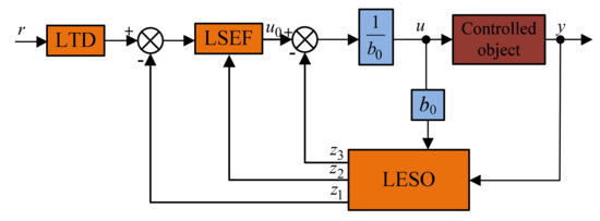
Figure 5.
Structure diagram of LADRC.
3.1. Design of LADRC Based on RLESO
In order to design the LADRC controller, Equation (4) can be transformed into a differential equation as follows:
Equation (8) is a second-order differential equation. Therefore, a second-order LADRC is designed. Let b0 = 3/(2LC), record the internal parameter uncertainty, time variable, and external disturbance in the system (8) as the total disturbance, and then the total disturbance is as follows:
Let Udc = y, igd = igd*, u = igd*, then Equation (8) can be transformed into the following mathematical model:
Let x1 = , x2 = , x3 = f, then Equation (10) can be transformed into the following state space description:
Therefore, the third-order continuous LESO corresponding to Equation (11) can be obtained:
In Equation (12), z1, z2, and z3 are the observed values of , , and f respectively; and l1, l2, and l3 are the observer gains. Since the DC link voltage (y) can be observed at any time, the corresponding structure can be deleted from Equation (12), and the difference between the differential of the DC link voltage and the corresponding state estimated by the observer can be corrected as feedback. Thus, the reduced-order linear extended state observer (RLESO) is obtained:
where z1 is the observation value for , and z2 is the observation value for f. Selecting the appropriate observer gain, the observer will be able to track and f in real time.
The disturbance compensation and LSEF of RLESO are designed as follows:
where KP and Kd are the parameters of the controller and r is the given value of the LADRC input. At this time, if the observation error of z2 to f is ignored, the system (10) can be simplified as an integral series structure. Therefore, the expected transfer function of the controlled object is as follows:
According to the pole assignment method in [25], the following pole assignment can be done for Equations (13) and (15):
where ωo and ωc are the bandwidth of the observer and controller, respectively.
According to Equations (13) and (14), the structure block diagram of LADRC based on RLESO is shown in Figure 6.
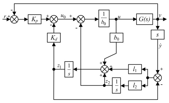
Figure 6.
Structure diagram of LADRC based on RLESO.
3.2. Design of the Improved LADRC Structure
In LADRC, the total disturbance observation ability of LESO is an important factor affecting the control quality of LADRC. The stronger the observation ability, the better the robustness and anti-interference ability of LADRC. This section analyzes and improves RLESO in terms of the disturbance observation capabilities.
3.2.1. Characteristic Analysis of RLESO
From Equations (13) and (16), the transfer functions of z1 and z2 in RLESO are obtained as follows:
By Laplace transformation of Equation (10), the total disturbance f can be written as:
According to Equations (18) and (19), the transfer function of the disturbance observation of RLESO is as follows:
Figure 7 shows the comparison of the traditional LESO and RLESO disturbance observation capabilities. Compared with traditional LESO, the bandwidth of RLESO is increased, and the disturbance observation ability of LESO is improved. At the same time, the phase lag of RLESO is reduced. However, the attenuation degree of its high-frequency band is reduced, which makes LESO vulnerable to high-frequency noise.
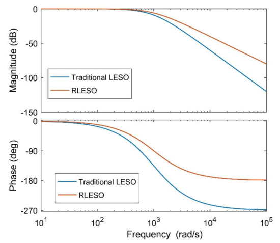
Figure 7.
Comparison of the disturbance observation capabilities between traditional LESO and RLESO.
3.2.2. Design of the Improved RLESO
Although RLESO improves the disturbance observation ability of the observer to a certain extent and reduces the phase lag of disturbance observation, it also enhances the noise amplification phenomenon. For this reason, referring to the classical control theory, a lead lag correction is added to the total disturbance. Therefore, following equation is obtained:
where z3 is the output of the correction link, Te is the time constant of the lead lag correction link, and α is the coefficient greater than zero.
According to Equations (13) and (21), the state space expressions of the improved RLSEO is as follows:
From Equations (20) and (21), the transfer function of the disturbance observation of the optimized RLESO is obtained as follows:
Figure 8 compares the disturbance observation capabilities of the improved RLESO and conventional RLESO. It can be seen that after adding the correction link, the high-frequency gain of RLESO is reduced, and the phase lag is basically unchanged. The noise amplification effect of RLSEO has been alleviated to some extent.

Figure 8.
Comparison of the disturbance observation capabilities between RLESO and the improved RLESO.
The disturbance compensation and LSEF of the improved RLESO are designed as follows:
From Equations (22) and (24), the structure block diagram of the improved LADRC is shown in Figure 9.
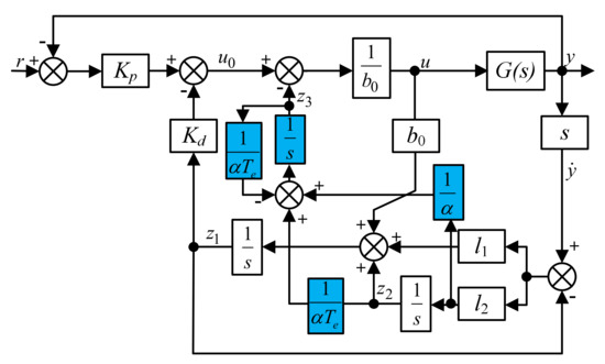
Figure 9.
Structure block diagram of the improved LADRC.
4. Analysis of the Frequency Domain Characteristics of Improved LADRC
4.1. Analysis of the Convergence and Estimation Error of Improved RLESO
Let the tracking error be , . According to Equations (18) and (21), the observation error of the DC link voltage differential and total disturbance are as follows:
Let the output value y and the control quantity u both take the step signal of the amplitude K, then their Laplace transform formulas are Y(s) = K/s and U(s) = K/s, respectively. Therefore, the steady-state errors of the DC link voltage differential and total disturbance are as follows:
The upper formula shows that under the condition of steady state, the improved RLESO can accurately track the actual value of the system and has good convergence.
4.2. Analysis of Anti-Interference Ability of Improved LADRC
According to Equations (18), (21), and (24), the transfer function of the control variable u is as follows:
where:
According to Equations (10) and (28), the simplified structure diagram of the improved LADRC is designed as follows:
From Figure 10, the closed-loop transfer function of the system is as follows:
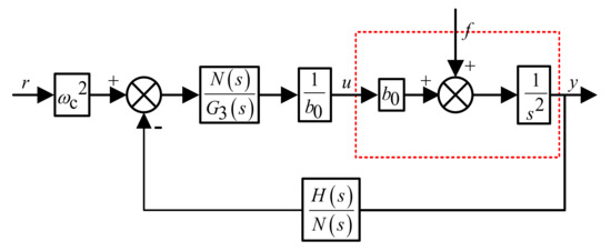
Figure 10.
Simplified structure diagram of the improved LADRC.
If the total disturbance f can be fully estimated, the output of the power network-side converter is only related to the controller bandwidth ωc. By adjusting ωc, the system can track the given value r quickly and without overshoot.
Figure 11 shows the frequency domain characteristic curve of the disturbance term. Compared with LADRC based on RLESO, the gain of the system in the middle and low frequencies is reduced after adding the correction link, and the anti-disturbance performance of the improved LADRC in the middle- and low-frequency band is enhanced. At the same time, with the increase of Te, the anti-interference performance of the system is gradually enhanced, and the degree of phase lag is gradually reduced.
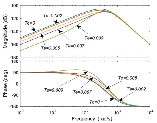
Figure 11.
Frequency domain characteristics of the disturbance term of the improved LADRC.
4.3. Analysis of the Anti-Disturbance Capability of the Improved LADRC in the PMSG System
The stability of the DC link voltage in PMSG is mainly affected by power network voltage mutation and load current disturbance [26]. In this article, the anti-interference ability of the DC link voltage to the load current is compared between the conventional LADRC and improved LADRC. Figure 12 is the structure diagram of the power network-side converter controlled by LADRC. Thus, the transfer function of the DC link voltage of PMSG is as follows:
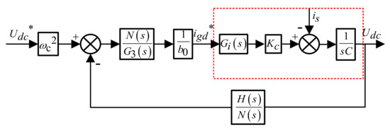
Figure 12.
Equivalent control block diagram of the grid-side converter.
In Equation (30), Gi(s) is the equivalent transfer function of the current inner loop, and Kc is the conversion link coefficient. It can be known from [27] that when the current inner loop adopts PI control, its equivalent transfer function Gi(s) = 1/(3T + 1), where T is the time constant of the equivalent transfer function of the inner ring.
Figure 13 shows the comparison of the frequency domain characteristic curves of the improved LADRC and traditional LADRC. The anti-disturbance ability of the improved LADRC is better than that of the conventional LADRC in the middle- and low-frequency band; the two curves in the high-frequency band are roughly coincident, so the improved LADRC will not affect the high-frequency gain.
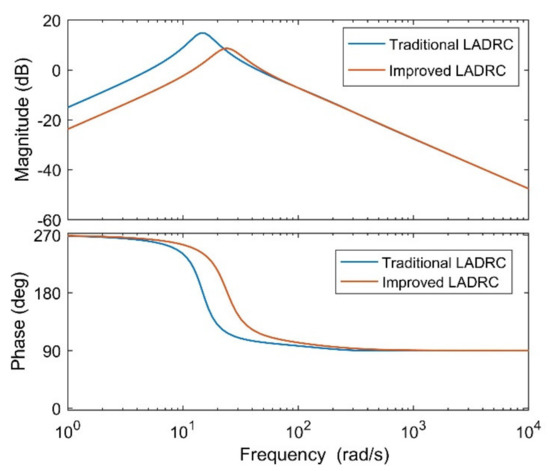
Figure 13.
Frequency domain characteristics of improved LADRC and traditional LADRC.
4.4. Stability Analysis of the DC Bus Voltage of the Improved LADRC
From Equation (30), the closed-loop transfer function from the given value Udc* of the DC bus voltage to DC bus voltage Udc can be simplified as follows:
where:
Because ωo, ωc, Te, T, Kc, b0, and α are all positive numbers, ai > 0, i = 0, 1, 2, 3, 4, 5. Based on the Linard–Chipat stability criterion, the following algebraic relations can be obtained:
where:
Equation (32) represents a stable system. Through numerical simulation of Equation (32), it can be found that when the system controller gain b0 is determined, when ωo and ωc are changed in a wide range, the stability of the DC link voltage of PMSG is not affected. In addition, under the condition that the system controller gain b0 is uncertain, by reasonably configuring ωo, ωc, and b0, the bus voltage can still have a good stability margin.
5. Simulation Analysis
In order to verify the correctness of the above-mentioned improved LADRC theoretical analysis, a 1.5 MW PMSG model was built based on MATLAB simulation software. The voltage outer loop is an improved LADRC, and the current inner loop is a traditional PI regulation. The specific parameters of PMSG are shown in Table A1.
5.1. Parameter Tuning of Controller
The performance of the LADRC controller has a great relationship with the selection of parameters. If the parameters are not selected properly, the performance of the LADRC controller will be reduced, and then the control effect of the DC bus voltage will be affected. In order to achieve the best performance of LADRC, through a lot of simulation experience, the following parameter tuning rules are summarized as follows:
- According to b0 = 3/(2LC), the control gain b0 = 52,083 can be obtained.
- The multiple relationship between the LESO bandwidth ωo and the controller bandwidth ωc is determined: ωo = 1~3ωc.
- When a set of ωo and ωc is obtained, l1~l3, Kp, and Kd are calculated according to the pole assignment equation of Equations (16) and (17).
- Increase ωo and ωc proportionally until the noise cannot bear to cause the system output fluctuation or oscillation, and then appropriately reduce the value of ωo and ωc to take into account the dynamic performance and stability of the controlled object. Further, if necessary, independently fine tune ωo and ωc until the dynamic response and anti-interference ability of the system meet the requirements.
- Reduce l1 and l2 and increase l3 appropriately until the dynamic characteristics of the controlled object can achieve the desired dynamic performance without overshoot. Record a set of parameters set at the current b0 value. Adjust Kp and Kd according to the need to obtain a better dynamic performance.
- Adjust b0 appropriately, and then adjust it again according to the above steps, and get a set of optimal parameters by comparison
Through the above parameter tuning method, the parameters of the controller shown in Table A2 were obtained.
5.2. Comparative Simulation Analysis of the Anti-Disturbance Capability
In order to analyze the immunity ability of the DC link voltage under the improved LADRC strategy and the conventional LADRC strategy, the following four low-voltage rides through (LVRT) faults were established based on MATLAB simulation software:
- (i)
- The voltage of the power network has a symmetrical low-voltage ride through fault, and the drop amplitude is 0.3 p.u. and the duration is 0.3 s;
- (ii)
- The voltage of the power network has a symmetrical low-voltage ride through fault, and the drop amplitude is 0.6 p.u. and the duration is 0.3 s;
- (iii)
- The voltage of the power network has an asymmetric low-voltage ride through fault, and the drop amplitude is 0.3 p.u. and the duration is 0.3 s;
- (iv)
- The voltage of the power network has an asymmetrical low-voltage ride through fault, and the drop amplitude is 0.6 p.u. and the duration is 0.3 s.
Scenario 1
Figure 14 shows the power network voltage waveform and DC link voltage waveform when the power network voltage drops by 0.3 p.u. symmetrically. When it is set at 0.7 s, the power network voltage will fall symmetrically and return to normal after 0.3 s. At the moment of fault, the overshoot of DC link voltage controlled by conventional LADRC is about 0.01 p.u., and that of the improved LADRC is close to 0.006 p.u.; at the moment of fault recovery, the drop amplitude of DC link voltage controlled by the conventional LADRC is about 0.012 p.u., and that of the improved LADRC is close to 0.007 p.u.
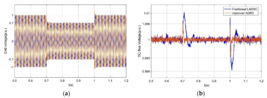
Figure 14.
Power network voltage waveform and DC link voltage waveform when the power network voltage drops by 0.3 p.u. symmetrically: (a) Waveform of the power network voltage; (b) Waveform of the DC link voltage.
Scenario 2
Figure 15 shows the power network voltage waveform and DC link voltage waveform when the power network voltage drops by 0.6 p.u. symmetrically. When it is set at 0.7 s, the grid voltage will fall symmetrically and return to normal after 0.3 s. At the moment of fault, the overshoot of the DC link voltage controlled by the conventional LADRC is about 0.03 p.u., and that of the improved LADRC is close to 0.015 p.u.; at the moment of fault recovery, the drop amplitude of the DC link voltage controlled by the conventional LADRC is about 0.03 p.u., and that of the improved LADRC is close to 0.017 p.u.
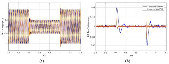
Figure 15.
Power network voltage waveform and DC link voltage waveform when the power network voltage drops by 0.6 p.u. symmetrically: (a) Waveform of the power network voltage; (b) Waveform of the DC link voltage.
Scenario 3
Figure 16 shows the waveform of the power network voltage and DC link voltage when the power network voltage drops by 0.3 p.u. asymmetrically. When it is set at 0.7 s, the grid voltage asymmetrical drop fault occurs, and it returns to normal after 0.3 s. At the moment of fault, the overshoot of the DC link voltage controlled by the conventional LADRC is about 0.0061 p.u., and that of the improved LADRC is close to 0.0057 p.u.; during the fault period, the DC link voltage fluctuation range of the conventional LADRC control is about 0.9955~1.0049 p.u., and the DC link voltage fluctuation range of the improved LADRC control is close to 0.9965~1.0038 p.u.; at the moment of fault recovery, the DC bus voltage overshoot of the conventional LADRC control is about 0.0073 p.u., and that of the improved LADRC is close to 0.0065 p.u.
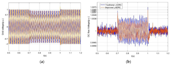
Figure 16.
Power network voltage waveform and DC link voltage waveform when the power network voltage drops by 0.3 p.u. asymmetrically: (a) Waveform of the power network voltage; (b) Waveform of the DC link voltage.
Scenario 4
Figure 17 shows the waveform of the power network voltage and DC link voltage when the power network voltage drops by 0.6 p.u. asymmetrically. When it is set at 0.7 s, the grid voltage asymmetrical drop fault occurs, and it returns to normal after 0.3 s. At the moment of fault, the overshoot of the DC link voltage under conventional LADRC control and improved LADRC control is close to 0.011 p.u.; during the fault period, the fluctuation range of the DC link voltage controlled by the conventional LADRC is about 0.99~1.0099 p.u., and that of the improved LADRC is close to 0.9932~1.0078 p.u.; at the moment of fault recovery, the overshoot amplitude of the DC link voltage controlled by the conventional LADRC is about 0.0245 p.u., and that of the improved LADRC is close to 0.0194 p.u.

Figure 17.
Power network voltage waveform and DC link voltage waveform when the power network voltage drops by 0.6 p.u. asymmetrically: (a) Waveform of the power network voltage; (b) Waveform of the DC link voltage.
The simulation results show that compared with the traditional LADRC, the improved LADRC has a better control effect on the DC link voltage in the case of the low-voltage ride through fault; that is, the improved LADRC can greatly enhance the anti-disturbance performance of PMSG.
6. Conclusions
The stability of DC bus voltage is key to safe and efficient operation of the PMSG system. In order to suppress the wide range of fluctuation of the DC bus voltage under disturbance, an LADRC based on an improved RLESO was proposed. The main contributions of this paper are as follows:
- (i)
- In order to reduce the phase lag and enhance the disturbance observation performance of the observer, an RLESO with a bus voltage differential and its observation error as feedback was designed. By introducing a lead lag correction in the total disturbance channel, the noise amplification phenomenon of the observer was enhanced, and the anti-disturbance performance of the improved LADRC was improved.
- (ii)
- The improved LADRC was applied to the voltage outer loop control of the power network-side converter of PMSG, which improved the stability of the DC bus voltage.
- (iii)
- The simulation results showed that under the condition of power network voltage symmetrical low-voltage ride through fault and asymmetrical low-voltage ride through fault, the control performance of the improved LADRC to DC bus voltage is better than that of the traditional LADRC.
The control strategy mentioned in this paper has proved its feasibility and effectiveness mainly through theoretical analysis and digital simulation, but it has not yet been applied to actual physical systems. Thus, our future research focus will be to verify the feasibility of the proposed control strategy through physical experiments.
Author Contributions
Conceptualization, X.Z. and Y.Z.; methodology, Y.Z.; software, Y.M.; validation, X.Y., L.Y. and B.Z.; data curation, L.Y. and B.Z.; writing—original draft preparation, Y.Z.; writing—review and editing, Y.Z. and X.Y.; visualization, Y.M.; supervision, X.Y. and L.Y.; funding acquisition, X.Z. All authors have read and agreed to the published version of the manuscript.
Funding
This work was funded by National Natural Science foundation of China (No. 51877152) and Natural Science Foundation of Tianjin of China (No. 18JCZDJC97300).
Acknowledgments
The authors are grateful to the support by the National Natural Science foundation of China (No. 51877152), Natural Science Foundation of Tianjin of China (No. 18JCZDJC97300) and Tianjin University of Technology for their support.
Conflicts of Interest
The authors declare no conflict of interest.
Abbreviations
| Acronym | Definition |
| PMSG | Permanent magnet synchronous generator |
| DC | Direct current |
| AC | Alternating current |
| PI | Proportional integral |
| PID | Proportional integral differential |
| LADRC | Liner active disturbance rejection control |
| LESO | Linear extended state observer |
| LSEF | Linear state error feedback |
| SVPWM | Space Vector Pulse Width Modulation |
| PWM | Pulse width modulation |
| LVRT | Low voltage ride through |
Appendix A

Table A1.
Main parameters of PMSG.
Table A1.
Main parameters of PMSG.
| Symbol | Description | Value |
|---|---|---|
| Base power | 1.5 MW | |
| Base voltage | 690 V | |
| Base frequency | 50 Hz | |
| DC link voltage | 1070 V | |
| DC link capacitor | 240 μF | |
| power network side equivalent resistance | 0.942 Ω | |
| power network side filter inductance | 0.12 mH | |
| Correction link time constant | 0.004 s | |
| Correction factor | 0.2 | |
| Inner ring equivalent time constant | 0.0025 s | |
| Conversion link coefficient | 0.85 |
Table A2.
Controller parameters.
Table A2.
Controller parameters.
| Symbol | Description | Value |
|---|---|---|
| Controller bandwidth | 500 | |
| Observer bandwidth | 2300 | |
| Inner loop proportionality coefficient | 0.9 | |
| Inner loop integration coefficient | 12 |
References
- Chen, J.; Yao, W.; Zhang, C.K.; Ren, Y.X.; Jiang, L. Design of robust MPPT controller for grid-connected PMSG-Based wind turbine via perturbation observation based nonlinear adaptive control. Renew. Energy 2019, 134, 478–495. [Google Scholar] [CrossRef]
- Jlassi, I.; Cardoso, A.J. Fault-Tolerant Back-to-Back Converter for Direct-Drive PMSG Wind Turbines Using Direct Torque and Power Control Techniques. IEEE Trans. Power Electron. 2019, 34, 11215–11227. [Google Scholar] [CrossRef]
- Zhang, J.Z.; Sun, T.J.; Wang, F.X.; Rodriguez, J.; Kennel, R. A Computationally Efficient Quasi-Centralized DMPC for Back-to-Back Converter PMSG Wind Turbine Systems Without DC-Link Tracking Errors. IEEE Trans. Ind. Electron. 2016, 63, 6160–6171. [Google Scholar] [CrossRef]
- Priyadarshi, N.; Ramachandaramurthy, V.K.; Padmanaban, S.; Azam, F. An ant colony optimized MPPT for standalone hybrid PV-wind power system with single Cuk converter. Energies 2019, 12, 167. [Google Scholar] [CrossRef]
- Zhang, Z.B.; Li, Z.; Kazmierkowski, M.P.; Rodriguez, J.; Kennel, R. Robust Predictive Control of Three-Level NPC Back-to-Back Power Converter PMSG Wind Turbine Systems with Revised Predictions. IEEE Tran. Power Electron. 2018, 33, 9588–9598. [Google Scholar] [CrossRef]
- Qais, M.H.; Hasanien, H.M.; Alghuwainem, S. A Grey Wolf Optimizer for Optimum Parameters of Multiple PI Controllers of a Grid-Connected PMSG Driven by Variable Speed Wind Turbine. IEEE Access. 2018, 6, 44120–44128. [Google Scholar] [CrossRef]
- Wang, W.; Lu, Z.X. Analysis of Model Predictive Current-Controlled Permanent Magnet Synchronous Motor Drives with Inaccurate DC Bus Voltage Measurement. Energies 2020, 13, 353. [Google Scholar] [CrossRef]
- Xiao, S.X.; Gu, X.; Wang, Z.L.; Shi, T.N.; Xia, C.L. A Novel Variable DC-Link Voltage Control Method for PMSM Driven by a Quasi-Z-Source Inverter. IEEE Trans. Power Electron. 2020, 35, 3878–3890. [Google Scholar] [CrossRef]
- Magne, P.; Marx, D.; Nahid-Mobarakeh, B.; Pierfederici, S. Large-Signal Stabilization of a DC-Link Supplying a Constant Power Load Using a Virtual Capacitor: Impact on the Domain of Attraction. IEEE Trans. Ind. Appl. 2012, 48, 878–887. [Google Scholar] [CrossRef]
- Wang, X.; Lin, H. DC-link current estimation for load-side converter of brushless doubly-fed generator in the current feedforward control. IET Power Electron. 2016, 9, 1703–1710. [Google Scholar] [CrossRef]
- Amin, M.M.; Mohammed, O.A. DC-Bus Voltage Control Technique for Parallel-Integrated Permanent Magnet Wind Generation Systems. IEEE Trans. Energy Convers. 2011, 26, 1140–1150. [Google Scholar] [CrossRef]
- Gu, B.; Nam, K.A. DC-link capacitor minimization method through direct capacitor current control. IEEE Trans. Ind. Appl. 2006, 42, 573–581. [Google Scholar]
- Da Silva, S.A.; Sampaio, L.P.; de Oliveira, F.M.; Durand, F.R. Feed-forward DC-bus control loop applied to a single-phase grid-connected PV system operating with PSO-based MPPT technique and active power-line conditioning. LET Renew. Power Gener. 2016, 11, 183–193. [Google Scholar] [CrossRef]
- Han, J.Q. From PID to active disturbance rejection control. IEEE Trans. Ind. Electron. 2009, 56, 900–906. [Google Scholar] [CrossRef]
- Han, J.Q. Active Disturbance Rejection Control Technique—The Technique for Estimating and Compensating the Uncertainties; National Defense Industry Press: Beijing, China, 2008. [Google Scholar]
- Wu, D.; Chen, K. Frequency-domain analysis of nonlinear active disturbance rejection control via the describing function method. IEEE Trans. Ind. Electron. 2013, 60, 3906–3914. [Google Scholar] [CrossRef]
- Xu, X.N.; Zhou, X.S.; Ma, Y.J.; Gao, Z.Q. Micro Grid Operation Controller Based on ADRC. High Volt. Eng. 2016, 42, 3336–3346. [Google Scholar]
- Gao, Z.Q. Active disturbance rejection control: A paradigm shift in feedback control system design. In Proceedings of the 2006 American Control Conference, Minneapolis, MN, USA, 14–16 June 2006; p. 7. [Google Scholar]
- Pan, Z.; Wang, X.; Wang, Z.; Tian, L.; Hoang, T.T. DC-Link Voltage Disturbance Rejection Strategy of PMW Rectifiers Based on Reduced-Order LESO. IEEE Access 2019, 7, 103693–103705. [Google Scholar] [CrossRef]
- Yang, Y.; Ma, L.; Huang, D.; Qin, N. Output Feedback Repetitive Learning Control of an Electrohydraulic Actuator of a Lower Limb Rehabilitation Exoskeleton. Comput. Sci. Eng. 2019, 21, 6–19. [Google Scholar] [CrossRef]
- Li, S.W.; Li, Y.L.; Sun, J.G.; Jin, Q.; Li, X.G. Power quality control method of micro grid based on control strategy of inverter distributed power supply. Grid Technol. 2010, 34, 6–11. [Google Scholar]
- Long, B.; Wang, W.; Huang, L.J.; Chen, Y.; Li, F.S.; Sun, H.B.; Li, H. Design and implementation of a virtual capacitor based DC current suppression method for grid-connected inverters. ISA Trans. 2019, 92, 257–272. [Google Scholar] [CrossRef]
- Herbst, G. A simulative study on Active Disturbance Rejection Control (ADRC) as a control tool for practitioners. Electronics 2013, 2, 246–279. [Google Scholar] [CrossRef]
- Chen, Z.Q.; Sun, M.W.; Yang, R.G. On the stability of linear active disturbance rejection control. Acta Autom. Sin. 2013, 39, 574–579. [Google Scholar] [CrossRef]
- Gao, Z.Q. Scaling and bandwidth-parameterization based controller tuning. In Proceedings of the IEEE 2003 American Control Conference, Denver, CO, USA, 4–6 June 2003; pp. 4989–4996. [Google Scholar]
- Zhou, X.S.; Liu, M.; Ma, Y.J.; Yang, B.; Zhao, F.Q. Linear Active Disturbance Rejection Control for DC Bus Voltage of Permanent Magnet Synchronous Generator Based on Total Disturbance Differential. Energies 2019, 12, 3906. [Google Scholar] [CrossRef]
- Ma, Y.J.; Yang, X.; Zhou, X.S.; Yang, L.Y.; Zhou, Y.L. Dual Closed-Loop Linear Active Disturbance Rejection Control of Grid-Side Converter of Permanent Magnet Direct-Drive Wind Turbine. Energies 2020, 13, 1090. [Google Scholar] [CrossRef]


© 2020 by the authors. Licensee MDPI, Basel, Switzerland. This article is an open access article distributed under the terms and conditions of the Creative Commons Attribution (CC BY) license (http://creativecommons.org/licenses/by/4.0/).