1. Introduction
Thermoelectric energy harvesting can power electronic systems autonomously from very low temperature differences. It has been shown that body heat can be used to power wireless sensors [
1] and consumer electronics [
2]. In the future, the temperature difference between day and night can also be used to power IoT nodes [
3]. In this application, the output voltage of the thermoelectric generator (TEG) changes polarity since the temperature difference between the thermal storage material and the environment switches polarity with the diurnal cycle.
The output voltage of the TEG is not high enough to directly operate CMOS transistors in most cases, so a DC/DC converter is needed. For autonomy, it is important that the converter can start up without the need of an external supply such as a battery. Systems with a single inductor [
4,
5] cannot start up at very low voltages and are not suitable for many autonomous low-power applications. All presently available systems which can start up from voltages below 100 mV are based on an oscillator with a transformer and a transistor with very low threshold voltage such as a native or depletion transistor or JFET (starting transistor). There are circuits available which can operate with bipolar input voltage and just one transformer [
6,
7], but they have poor performance (higher startup voltage and/or lower efficiency) compared to unipolar converters.
On the other hand, two-transformer solutions [
8,
9,
10] have a higher startup voltage and lower peak efficiency for two reasons: (1) When two unipolar converters are anti-parallelly connected, there is very high leakage through the unused starting transistor (problem 1), and (2) the parasitic body diodes of the unused starting and switching transistors are forward-biased (problem 2). In [
8,
9],
problem 2 could be eliminated by connecting two starting and two switching transistors anti-serially in both parts of the converter, but this has the drawback of a larger chip area and higher switching losses for a given on-resistance. For these reasons, the bipolar LTC3109 [
9] has worse performance compared to the unipolar LTC3108 [
11].
In this work, a two-transformer circuit is presented which is based on two anti-parallelly connected, state-of-the-art transformer reuse flyback converters [
12,
13]. Before the improvements of the new circuit (the used IC is named Mercury2) are explained, the typical topology of the former unipolar converter (IC Mercury) is briefly discussed and the most important differences in design are explained in the next section. The realization steps, how the two already mentioned problems were solved in the new design, will be explained in detail.
Section 3 shows a comparison with an available state-of-the-art bipolar converter (LTC3109). Experimental results are presented that show that good performance can be combined with high efficiency of the new design.
2. Materials and Methods
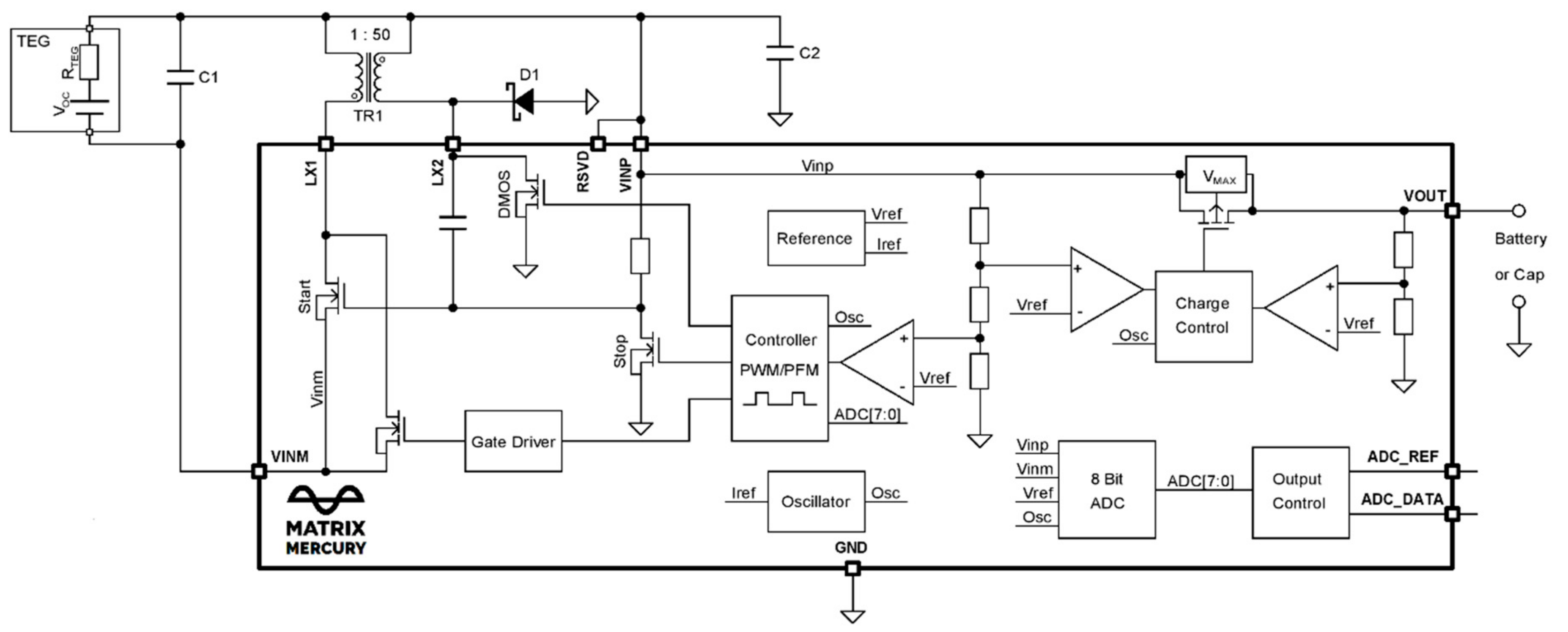
2.1. Unipolar Converter
Based on the patent [
12] of H.D., the unipolar converter Matrix Mercury [
13] in
Figure 1 uses a transistor-based Meissner oscillator [
14] consisting of the transformer TR1, a coupling capacitor, a biasing resistor and the native start transistor for ultra-low voltage startup.
The output voltage of the oscillator is rectified by the Schottky diode D1 and the external capacitor C2 is charged in a way that the GND potential is below the negative potential of the TEG. Once C2 is charged to a sufficient voltage (around 950 mV) to operate the analog and digital circuits, the Meissner oscillator is disabled by the stop transistor. This is possible because the gate of the start transistor is connected to the GND potential which is below the threshold voltage.
The transformer TR1, D1 and C2 are reused to form a flyback converter together with the LX1 switching transistor which is turned on by the controller via the bootstrapped gate driver. A DMOS switch in parallel to D1 forms a synchronous rectifier to increase efficiency. The flyback converter operates with constant frequency and duty cycle and provides a constant input resistance which can be adjusted for optimum impedance matching for a given TEG without additional measures [
1]. When the voltage at C2 is higher than the output voltage of the converter (V
OUT), the Charge Control circuit closes the PMOS transistor. This is done in such a way that the current is limited and the voltage at C2 always stays above 1.8 V. Once the maximum output voltage is reached, the controller switches to a pulse frequency modulation (PFM) scheme to maintain the output voltage.
An 8-bit analog-to-digital converter (ADC) measures the open circuit voltage (VOC) of the TEG every second. Just before each measurement, the flyback converter is stopped temporarily to charge the input capacitor C1 via the electrical resistance of the TEG (RTEG) up to VOC. The measurement result is used to determine the gate driver settings, whether the DMOS should be used and to stop the flyback converter at high VOC to prevent damage to the chip. If the ADC measurement result shows that the input power is insufficient to charge the battery or capacitor, the PMOS is opened and the IC powers down. In this state, only a very low leakage current enters the VOUT pin and stored energy in the battery or capacitor is not dissipated into the chip.
2.2. Bipolar Converter
Naive anti-parallel connection of two unipolar converters would require an additional transformer and an additional external capacitor next to the external capacitor C2. In [
12], it is shown that the secondary winding of TR1 can also be connected to the second terminal of the TEG. By using this approach for negative input voltages and a dual Schottky diode (D1), the resulting circuit in
Figure 2 just needs one additional transformer compared to the unipolar version.
For positive input voltages, the oscillator including transformer TR1 starts whilst the other oscillator with TR2 is stopped due to negative feedback. For negative input voltages, the opposite is true. In both scenarios, C2 is charged and the GND potential is below both TEG potentials. Once the controller is started, just the flyback converter with positive input voltage is operated. If the absolute value of VOC is too low for charging the output, the converter is disconnected as in the unipolar version.
Without additional improvements, this circuit would still have problems 1–2 described in the introduction.
2.3. Polarity Detector
The start transistor of the inactive oscillator has a very high leakage current since the gate voltage is around the threshold voltage of the native NMOS device. The resistance is in the range of 50 Ω and increases the startup voltage and decreases the efficiency. To eliminate this leakage current, it is simple to apply a negative gate source voltage to the transistor by turning on the stop transistor after startup.
For startup, it is essential that the turns ratio of the transformer is high enough to start oscillations. If this is the case, the most critical phase is when the supply voltage in C2 is between the threshold voltage of the transistors used in the analog part (around 650 mV) and the end of the startup phase (around 950 mV), where the bandgap reference and voltage detector are already started and the supply current increases. To get the same startup performance as a unipolar converter, it is necessary to deactivate the unused oscillator as quickly as possible.
Since comparators cannot work at this stage of startup, the idea is to use the oscillating signal of the working oscillator to deactivate the other oscillator. This is done by the circuit shown in
Figure 3.
The D-Flip-Flops with active low Reset 335 and 365 form together an edge triggered set and edge triggered reset Flip-Flop (marked yellow). The output “Vin1_high” is set by a rising edge on 335 and reset by a rising edge on 365. In this way, the working oscillator deactivates the other one via the OR-gate 332 or 382 and NMOS 322 or 372 and leakage is minimized. Since the oscillating signal on the clock input of the Flip-Flop exceeds the positive supply and goes below the GND potential, this circuit is already working at the minimum voltage necessary to hold the 1-bit information which is in weak inversion of the used transistors (around 450 mV).
When the output of the voltage detector 311 goes high, the second oscillator is turned off and the clock inputs of the D-Flip-Flops and the gates of the native NMOSs 304 and 354 are over-voltage-protected by the stop transistors 322 and 372. With this polarity detector, problem 1 is solved.
2.4. Bulk Connection to Gnd
In the unipolar converter, the bulks of the starting transistor and the LX1 switch can be connected to VINM. This is the best solution since there is no body effect, and the LX1 switches just need to be dimensioned for the input voltage which is much lower than the output voltage.
In the bipolar converter, the bulk voltage of the transistors of the unused converter would be higher than the drain voltage and the bulk drain diode would be forward-biased. In
Figure 4, this is avoided by connecting the bulks of both starting transistors 404 and 454 and the LX1 switches 420 and 470 to GND. Since the GND potential is always below Vin1 and Vin2, the parasitic diodes are never forward-biased and problem 2 is solved.
Unfortunately, this causes new issues:
2.5. Improved Bulk Connection
Figure 5 shows the improved bulk connection. Like in
Figure 4, the bulks of the starting transistors 504 and 554 are connected to GND. This causes a body effect with the rising output voltage, but in fact there is minor impact since the startup phase is stopped before reaching 1 V. During normal operation, the gates of 504 and 554 are connected to GND. They need to be dimensioned for the output voltage, which is no problem because the area is very small. This configuration brings the additional advantage that the starting transistors do not need to be in an isolated well in the p-substrate process used.
With the two PMOSs 537 and 538 and the level shifter 536, the voltage “Vin_min” is generated which is equal to the lower of the input voltage potentials. This voltage is connected to the bulks and the gate drivers of the LX1 switches 520 and 570. With this improvement, there is no body effect and no forward-biased MOS diode. The LX1 switches 520 and 570 only need to be dimensioned for the input voltage. In the used 180 nm production process, this gives a huge area and performance benefits since 1.8 V low-threshold transistors with L = 180 nm can be used instead of standard 5 V L = 500 nm transistors.
3. Results
For the following measurements, the TEG was replaced by a simple model consisting of a voltage source V
OC and a series resistor R
TEG like in the TEG symbol in
Figure 2. For a given V
OC and R
TEG, the maximum input power is P
MAX = V
OC2/(4 × R
TEG). The input power P
IN at any given operating point depends on the match between R
TEG and the presented input impedance of the circuit R
IN, such that P
IN/P
MAX = 4 × R
IN × R
TEG/(R
IN + R
TEG)
2.
This work was compared to LTC3109 [
9] and Mercury [
13]. LTC3109 [
9] is the only available commercial IC which can operate with very low bipolar input voltages and is also a two-transformer design. For low input voltages, LTC3109 performs best with 1:100 transformers. Mercury [
13] is a converter for unipolar input voltages and has best-in-class efficiency for low input voltages and low input power. Like this work, Mercury needs 1:100 transformers for very low-voltage startup at low R
TEG; at higher R
TEG, where the same input power produces higher input voltages, transformers with a lower turns ratio (1:50 and 1:20) can be used and efficiency is increased.
All ICs have a comparable VOUT range (Mercury + Mercury2: 2 V to 5 V, LTC3109: 2.35 V to 5 V), switching frequency (Mercury + Mercury2: 20 kHz, LTC3109: 10 kHz to 100 kHz) and VIN range (Mercury: up to VOC = 1 V, Mercury2: up to Voc = ±1 V, LTC3109: VIN = ±500 mV).
3.1. Startup Performance
The results in
Table 1 show the values for a fully depleted state of the system.
3.2. Efficiency Measurements
The same transformers specified in 3.1. were used for the following measurements. The plotted efficiency is the output power (P
OUT) divided by the maximum input power which is a multiplication of the electrical efficiency (P
OUT/P
IN) and impedance matching (P
IN/P
MAX). The setup is shown in
Figure 6: V
OUT is fixed by a source measure unit (SMU) and I
OUT is measured and used to calculate P
OUT.
The flyback converters of Mercury and Mercury2 (this work) were programmed to a frequency of 20 kHz and a duty cycle of 28% for an input resistance of 4 Ω.
Figure 7 shows the LX2A waveform with an LX1A switch on-time of 14 µs and a period of 50 µs. The DMOS A is switched on for 13 µs and turned off before the zero crossing of the secondary current.
LTC3109 with LPR6235 1:100 has an input resistance of approximately 4 Ω. Therefore, the used R
TEG = 4 Ω in
Figure 8 gives best results for the efficiency for this setup.
Compared to LTC3109, Mercury2 shows a much higher efficiency in the range of ~70%. Further, the minimum VOC for operation is much lower.
When compared to Mercury, Mercury2 shows a slightly higher efficiency at positive VOC. The efficiency is nearly equal for positive and negative input voltages. Note that Mercury does not work at negative VOC.
Figure 9 shows the efficiency graphs for R
TEG = 12 Ω. LTC3109 performs worse due to imperfect impedance matching. Mercury and Mercury2 use a frequency of 20 kHz and a duty cycle of 20% for an input resistance of 12 Ω. This is, for both ICs, the setup of the first mass production version.
In this case, the efficiency of Mercury and Mercury2 remains around 75% over a wide range of open circuit voltages, whereas the efficiency of the LTC3109 drops down to ~25%.
Figure 10 shows a comparison with Mercury since LTC3109 was not designed to work with an R
TEG = 60 Ω. This is the setup where both ICs achieve the highest efficiency, when they operate with a frequency of 20 kHz and a duty cycle of 14% for an input resistance of 60 Ω.
The highest efficiency values of ~85% can be seen when the open circuit voltage is in the range of 300 mV.
4. Discussion
The results show that for the startup voltage and efficiency, the performance of the unipolar converter could be reached. This confirms that the design improvements solve problems 1–2 and for the first time, a converter for ultra-low bipolar input voltages achieves the same performance as a unipolar converter.
Compared to Mercury [
13], a higher cold start V
OC input is required to start oscillations for the same transformer turns ratio at R
TEG = 60 Ω. The reason is that the resistive divider consisting of R
TEG and two starting transistors (around 50 Ω each) lowers the input voltage at high R
TEG significantly compared to the unipolar solution.
The higher peak efficiency compared to Mercury [
13] results from an improved layout of the LX1 switches. For R
TEG = 60 Ω, this has not much influence since the electrical resistance of the primary path is dominated by the 1:20 transformer.
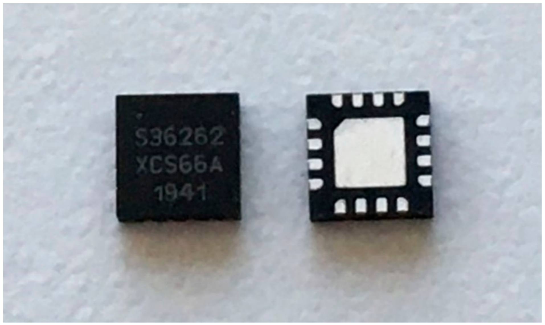
The Matrix Mercury2 IC is designed for a −40 °C to +85 °C operating temperature range and will be the first production bipolar converter chip which achieves the same performance as a unipolar converter. Mercury2 will be available in high volume in Q4 2020 in a QFN16 3 × 3 mm package (
Figure 11).
For electromechanical and piezoelectrical energy harvesters with low AC voltages and frequencies up to 1 kHz, also an IC called Mercury3 is planned which is based on Mercury2.
5. Conclusions
In this paper, an integrated novel converter topology is presented which can be used for ultra-low bipolar input voltages such as those generated during harvesting of thermoelectric energy. The circuit shown has the same self-starting and peak efficiency performance as the unipolar version without the use of additional large-area components. It is demonstrated that a bipolar converter can achieve the same performance as a unipolar converter. The new converter can start from a fully depleted state at a ±13 mV input and boost it to output voltages of up to 5 V. The experimental results demonstrate an efficiency of up to 85% and an almost perfect impedance matching over the entire input voltage range.
6. Patents
International patent application PCT/US2019/017898, H.D.; International patent application PCT/US2019/017900, H.D. and D.T.; US patent application 16/856697, H.D.
Author Contributions
Conceptualization, H.D. and D.T.; methodology, H.D.; validation, H.D.; formal analysis, H.D.; investigation, H.D.; data curation, H.D.; writing—original draft preparation, H.D.; writing—review and editing, B.D. and D.T.; visualization, H.D.; supervision, B.D.; project administration, H.D. All authors have read and agreed to the published version of the manuscript.
Funding
This research consists of two ICs: A test chip which was designed at TU Graz and was produced within the scope of the Europractise Mini@sic project (supported by EU’s Horizon 2020) and received no further external funding and a product chip which was developed at Cirtec Medical. This material is based upon work supported by DARPA under award Acquisition Services Directorate (AQD) number D19AC00002.
Acknowledgments
The authors thank Jasmin Gradincic for his layout support for the test chip and the team around Ashwath Pavithran from Cirtec Medical in Chandler, Arizona for the design of Mercury2.
Conflicts of Interest
The authors declare no conflict of interest. The funders had no role in the design of the study; in the collection, analyses, or interpretation of data; in the writing of the manuscript, or in the decision to publish the results.
References
- Meli, M.; Dillersberger, H. Efficiently harvesting energy from temperature differences in order to power wireless systems. In Proceedings of the Wireless Congress: Systems & Applications, Munich, Germany, 12–13 November 2014. [Google Scholar]
- PowerWatch. Available online: https://www.powerwatch.com (accessed on 1 September 2020).
- MATRIX PowerStation. Available online: https://www.matrixindustries.com/en/energy-harvesting (accessed on 1 September 2020).
- Gatti, A.; Spiazzi, G.; Gerosa, A.; Neviani, A.; Bevilacqua, A. A 130-nm CMOS Dual Input-Polarity DC-DC Converter for Low-Power Applications. IEEE Solid-State Circuits Lett. 2019, 2, 211–214. [Google Scholar] [CrossRef]
- Alhawari, M.; Mohammada, B.; Saleh, H.; Ismail, M. An Efficient Polarity Detection Technique for Thermoelectric Harvester in L-based Converters. IEEE Trans. Circuits Syst. I Rehular Pap. 2017, 64, 705–716. [Google Scholar] [CrossRef]
- Nachiket, V.D.; Ramadass, Y.K.; Chandrakasan, A.P. A Bipolar ±40 mV Self-Starting Boost Converter with Transformer Reuse for Thermoelectric Energy Harvesting. In Proceedings of the IEEE International Symposium on Low Power Electronics and Design (ISLPED), La Jolla, CA, USA, 11–13 August 2014; pp. 221–226. [Google Scholar]
- Cao, P.; Qian, Y.; Xue, P.; Lu, D.; He, J.; Hong, Z. An 84% Peak Efficiency Bipolar-Input Boost/Flyback Hybrid Converter with MPPT and On-Chip Cold Starter for Thermoelectric Energy Harvesting. In Proceedings of the IEEE International Solid-State Circuits Conference (ISSCC), San Francisco, CA, USA, 17–21 February 2019; pp. 420–422. [Google Scholar]
- Salerno, D.C.; Bazinet, J.P. Method and System for Polarity Independent Step-Up Converter Capable of Operating under Ultra-Low Input Voltage Condition. U.S. Patent Application US2010/0195360, 13 January 2010. [Google Scholar]
- LTC3109. Available online: https://www.analog.com/en/products/ltc3109.html (accessed on 1 September 2020).
- Rubio, E.; Hirish, S.H.; Nemir, D.C. Ultra-Low Voltage Boost Circuit. U.S. Patent Application US2010/0208498, 21 April 2010. [Google Scholar]
- LTC3108. Available online: https://www.analog.com/en/products/ltc3108.html (accessed on 1 September 2020).
- Dillersberger, H. Flyback Converter for Operation with Very Low Input Voltages. International Patent Application WO2014/060241, 17 October 2012. [Google Scholar]
- MATRIX Mercury. Available online: https://www.matrixindustries.com/en/products/mercury-energy-harvesting-boost-converter (accessed on 1 September 2020).
- Bohan, J.E. Low Voltage Driven Oscillator Circuit. U.S. Patent US4734658, 14 August 1987. [Google Scholar]
- Dillersberger, H. Starter Circuit for Energy Harvesting Circuits. International Patent Application PCT/US2019/017898, 13 February 2019. [Google Scholar]
| Publisher’s Note: MDPI stays neutral with regard to jurisdictional claims in published maps and institutional affiliations. |
© 2020 by the authors. Licensee MDPI, Basel, Switzerland. This article is an open access article distributed under the terms and conditions of the Creative Commons Attribution (CC BY) license (http://creativecommons.org/licenses/by/4.0/).


