Design and Implementation of Solar OLED Lighting Driver Circuit with Frequency Modulation Control


Abstract
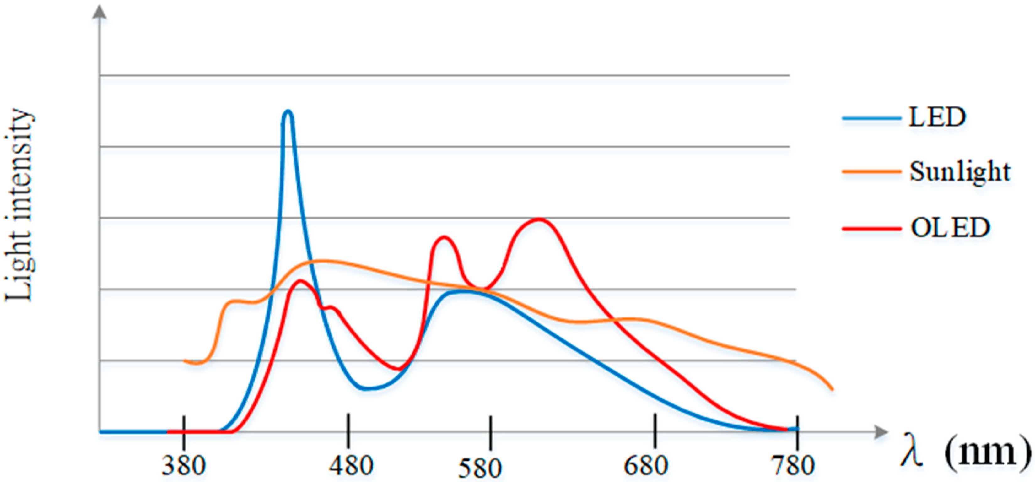
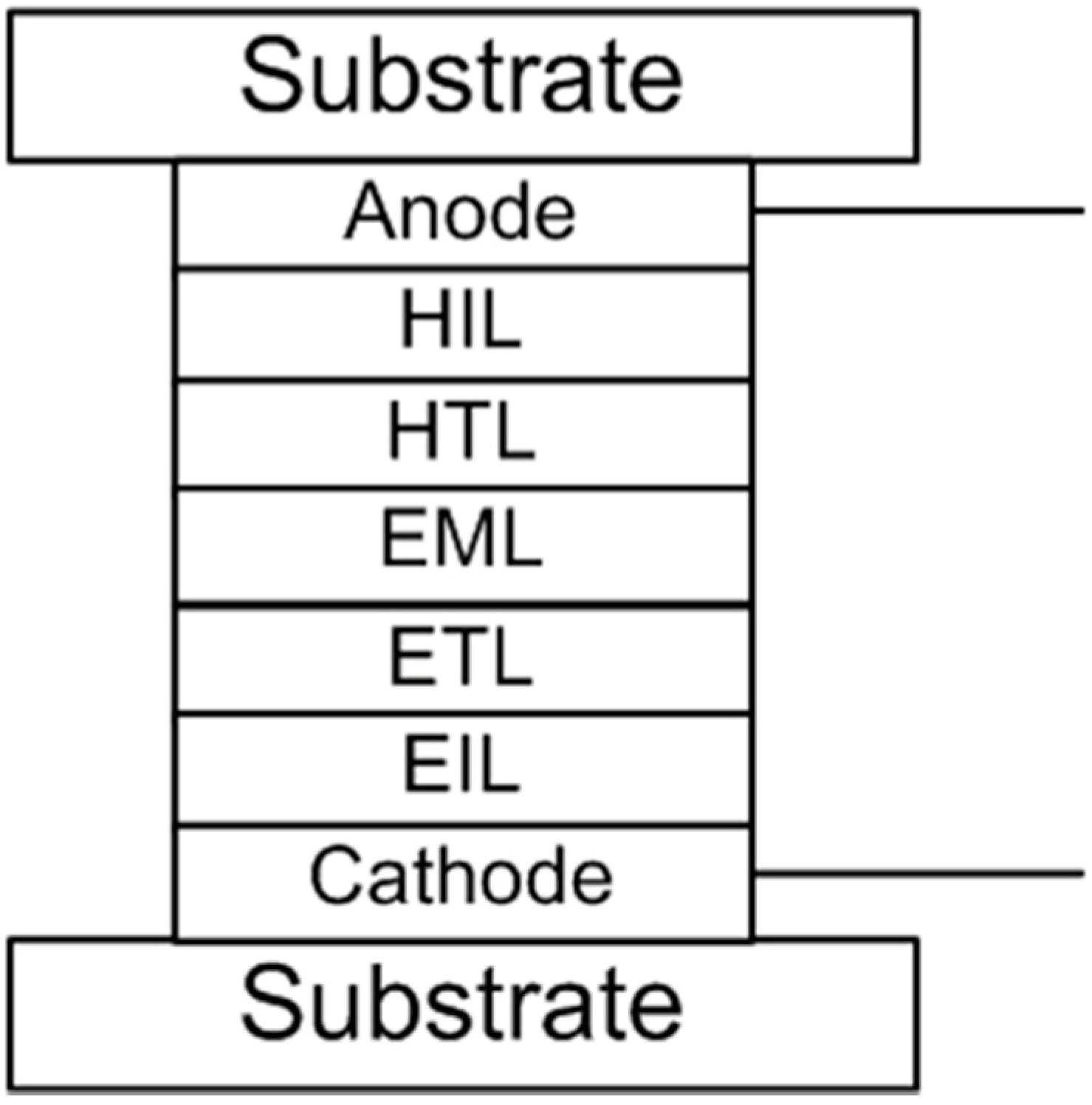
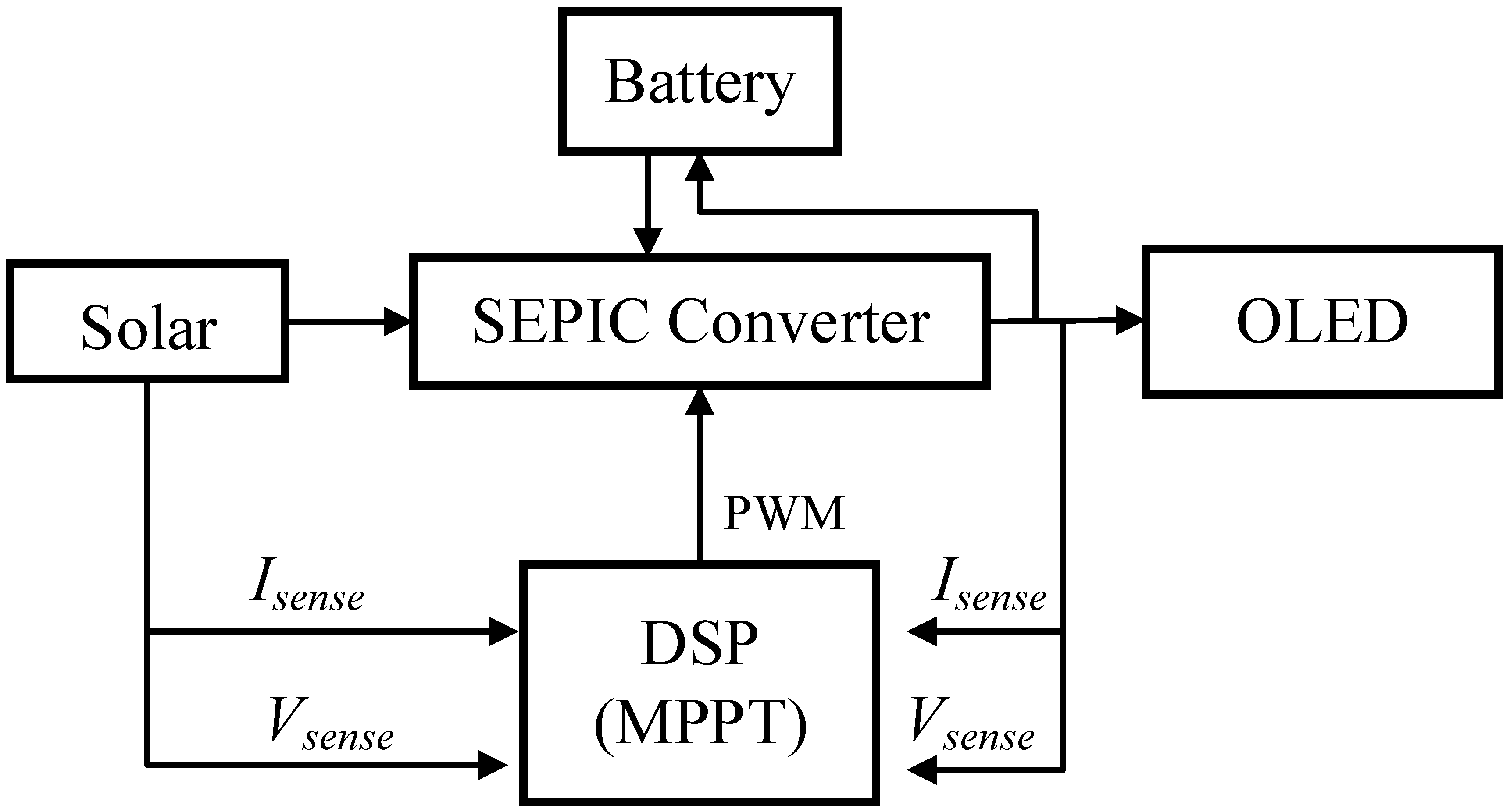
:1. Introduction
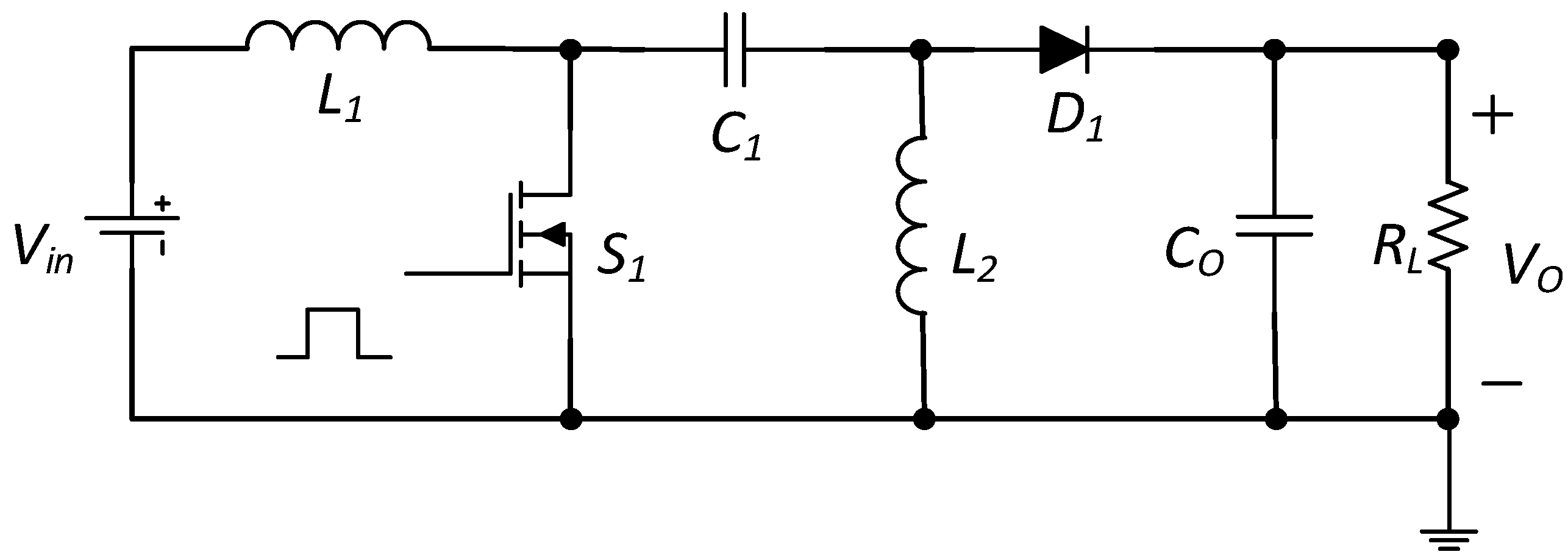
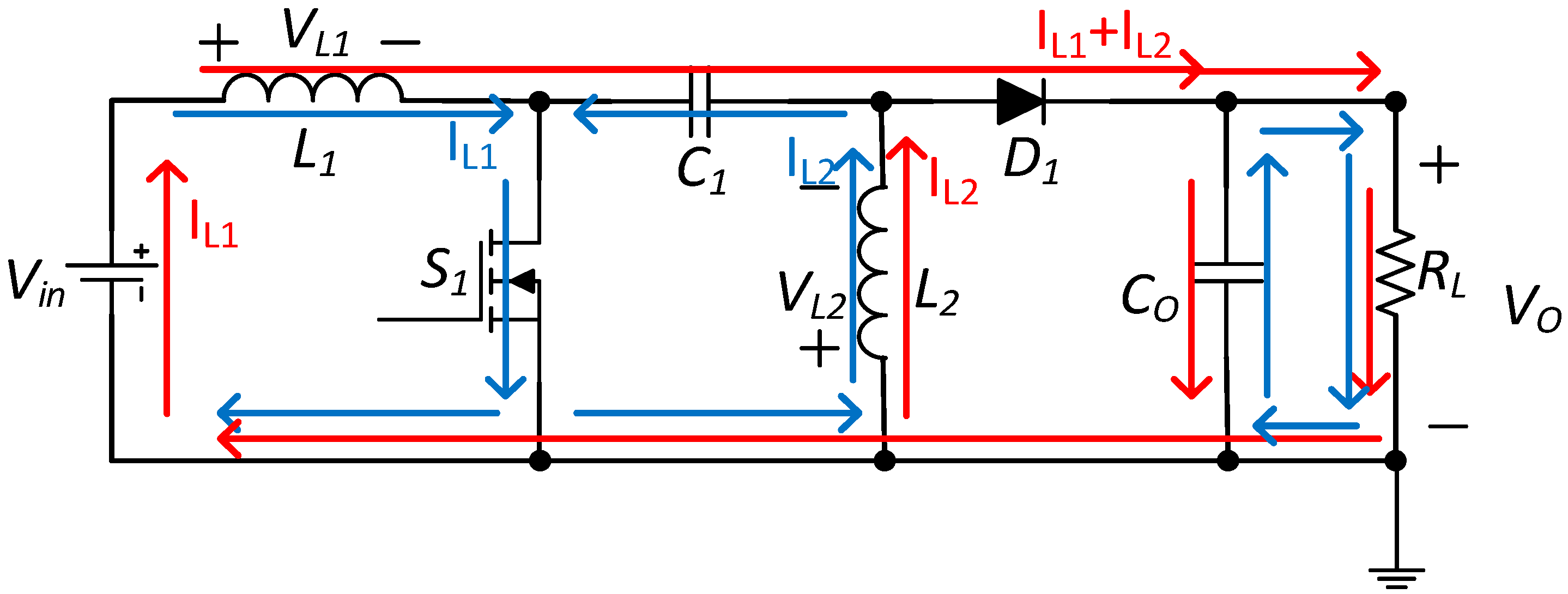
2. Original Single-Ended Primary Inductor Converter (SEPIC) Converter
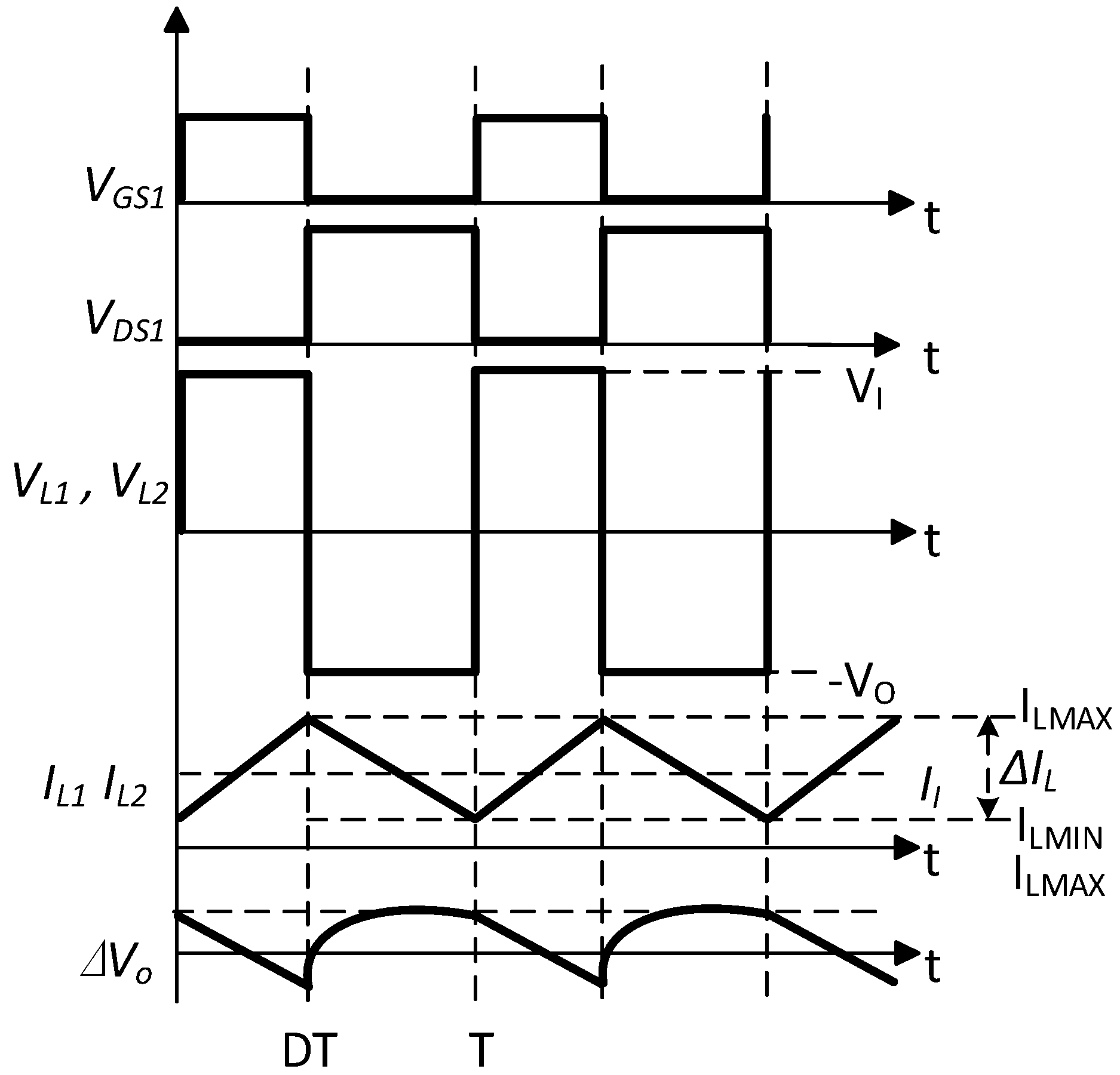
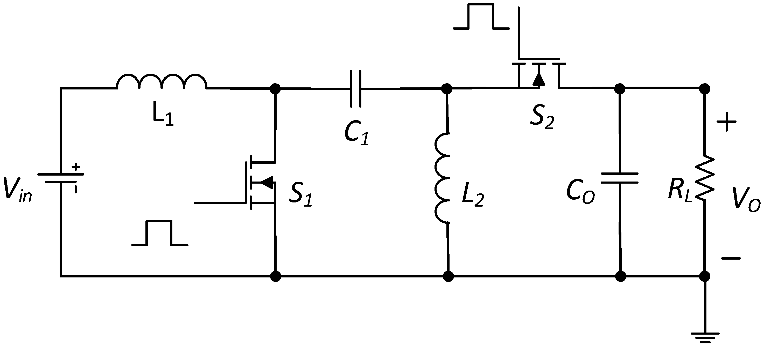
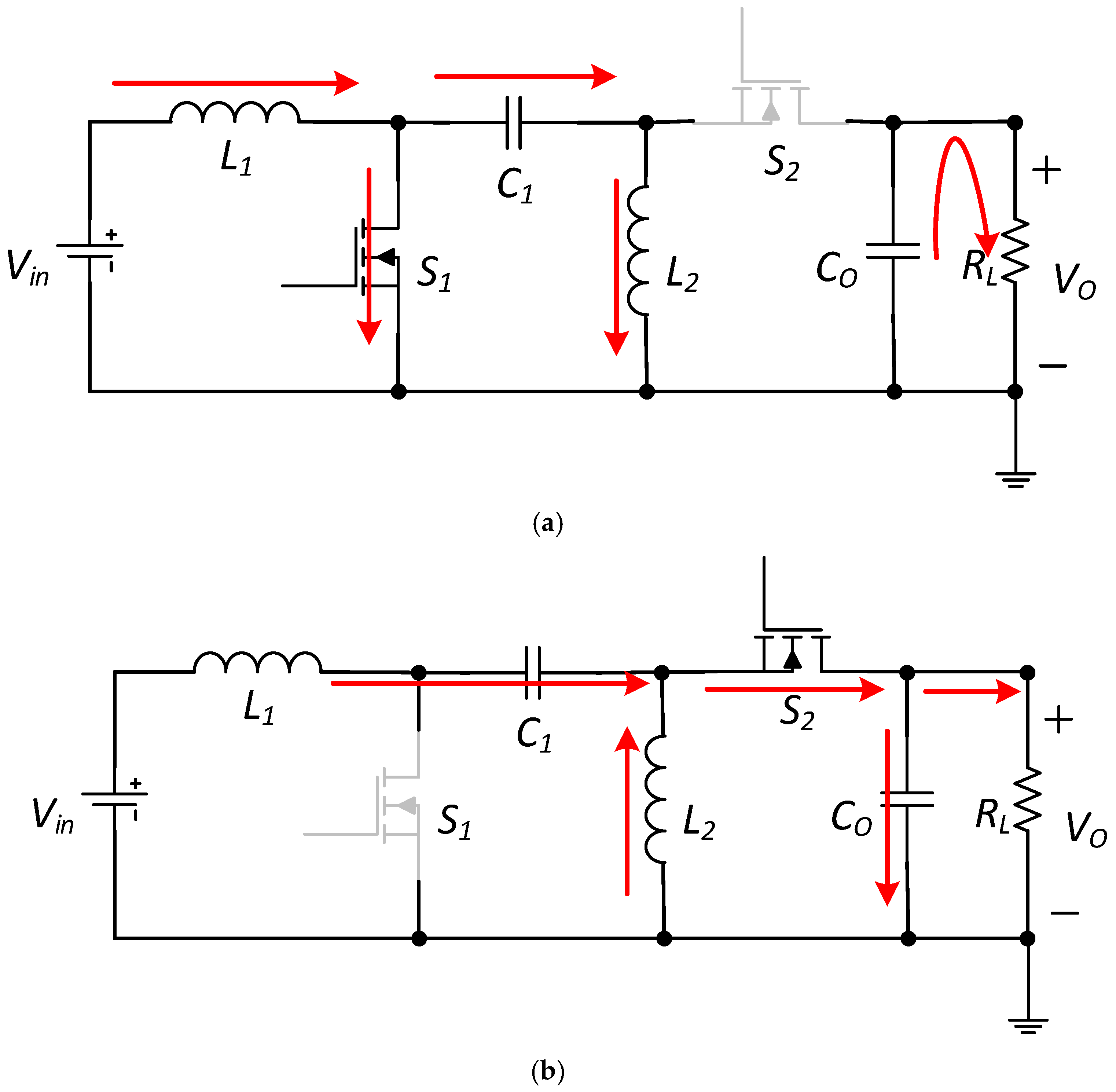
3. TCM SEPIC Converter with Zero Voltage Switching
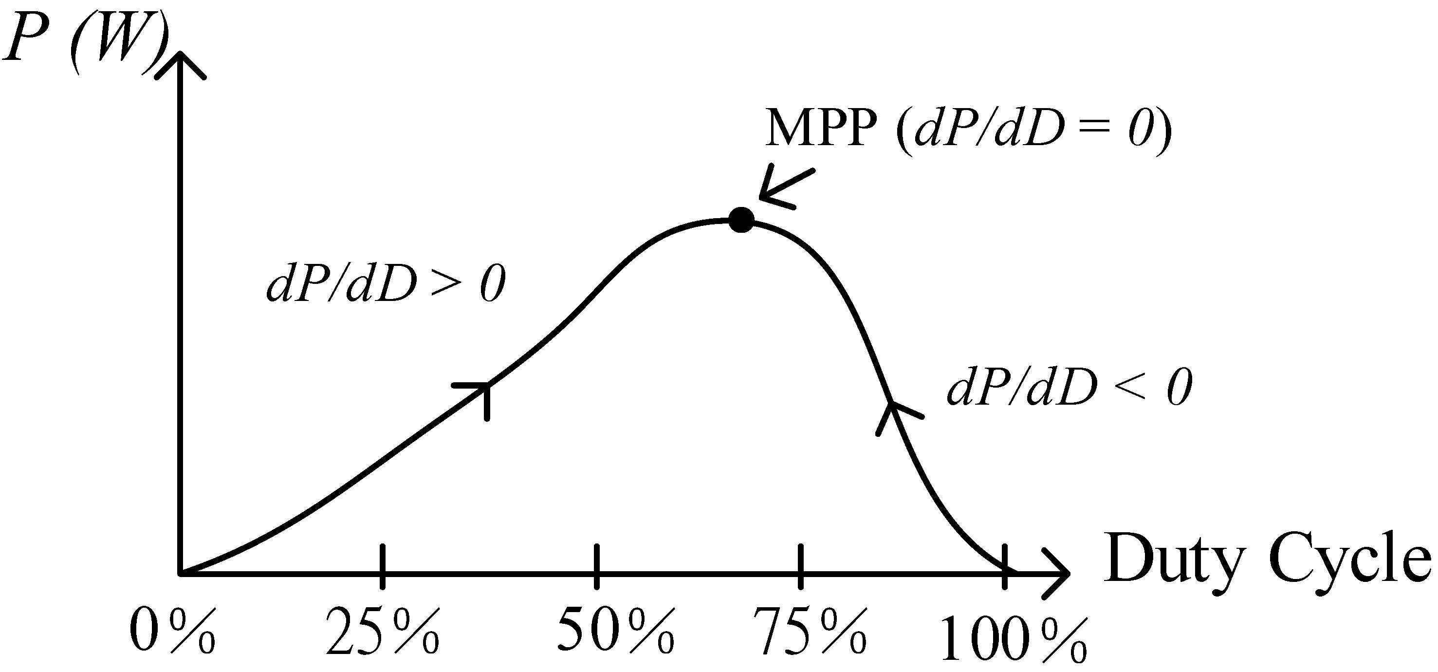
4. Digital Control Design
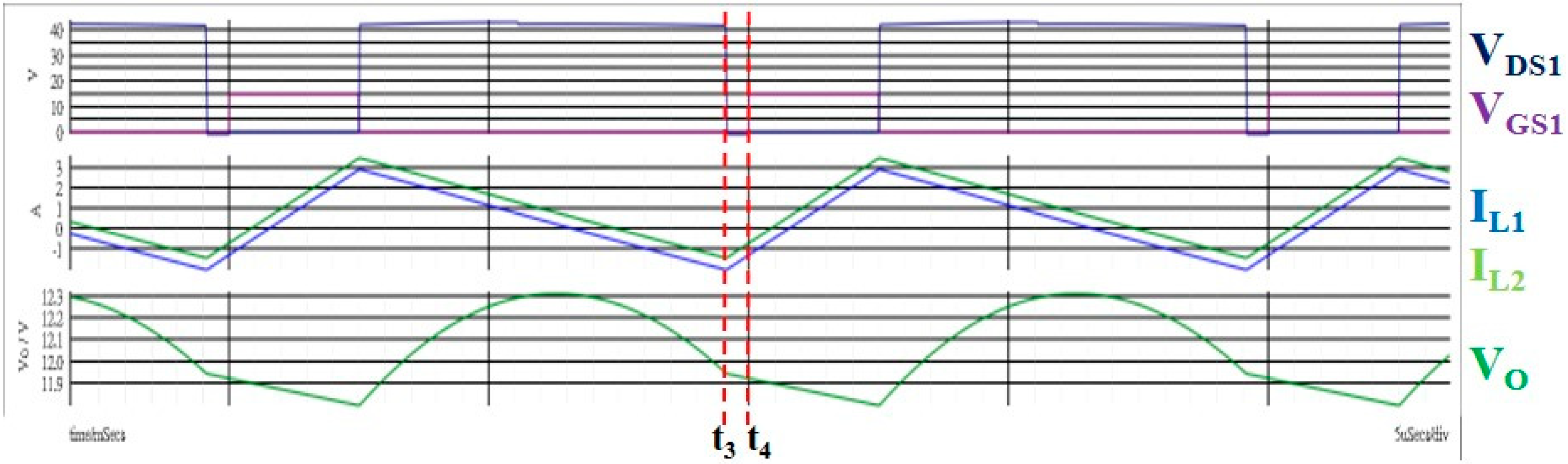
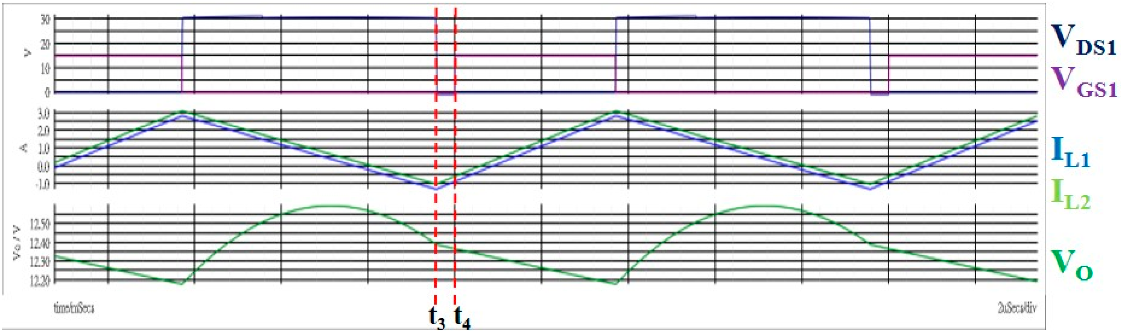
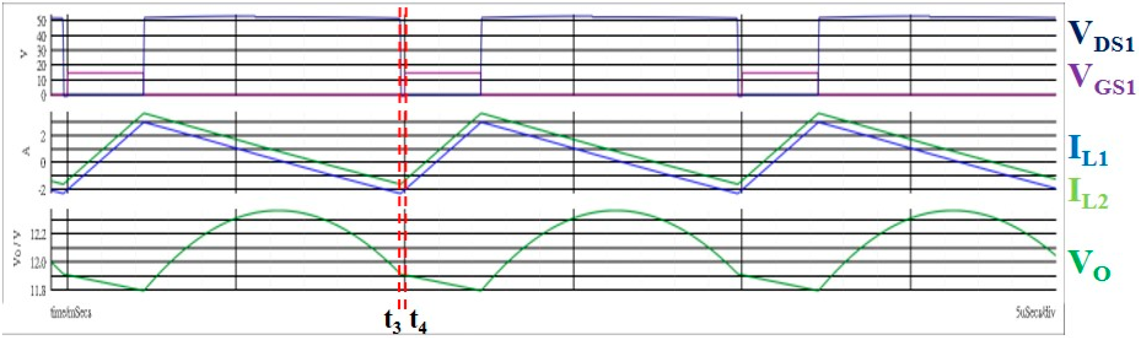
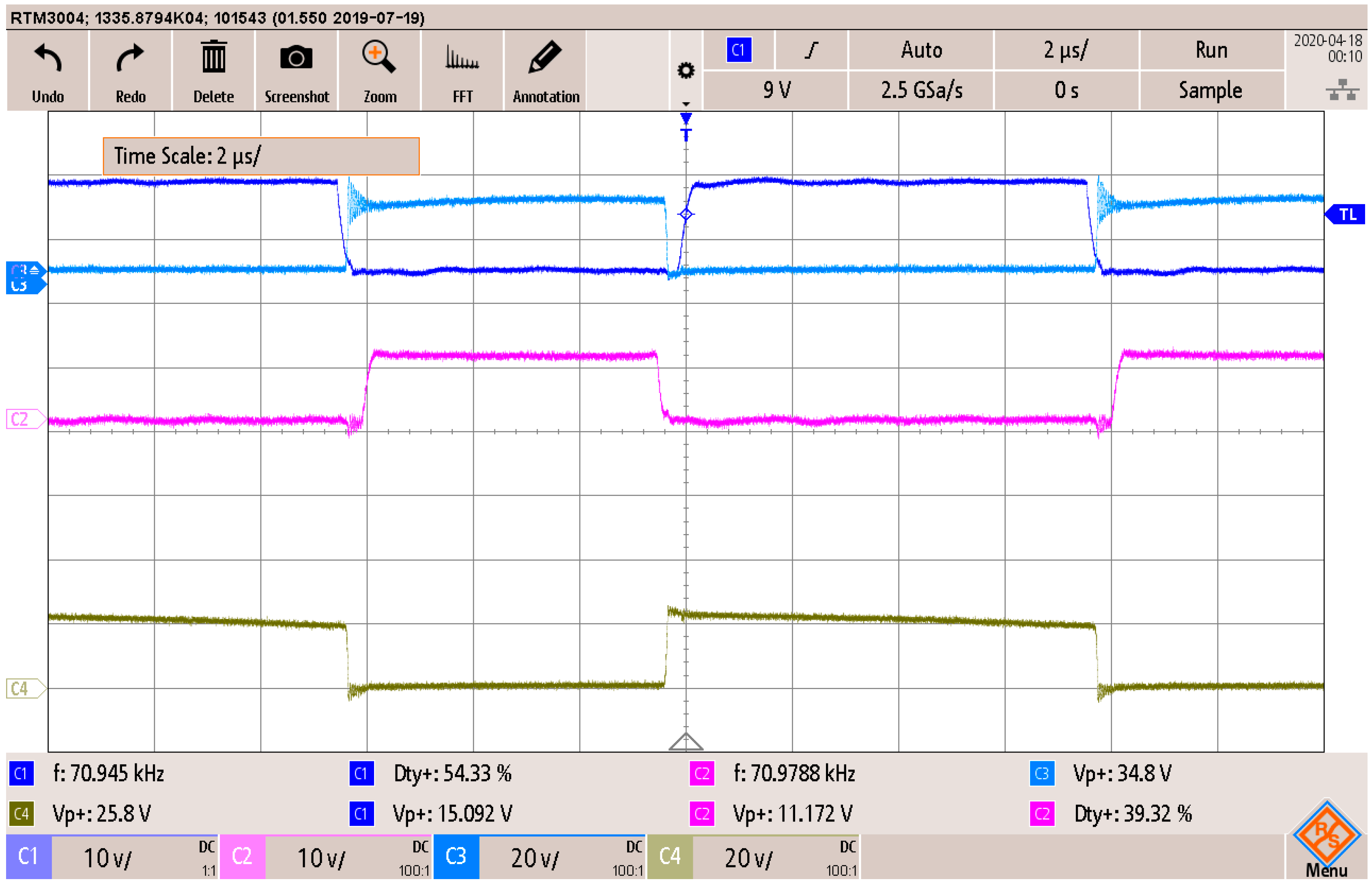
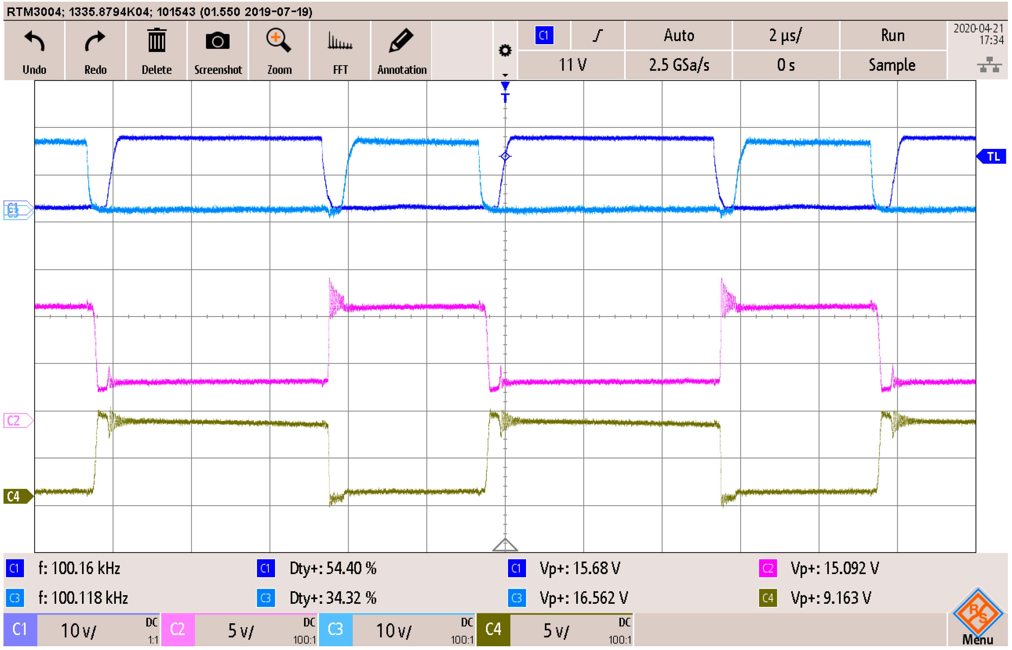
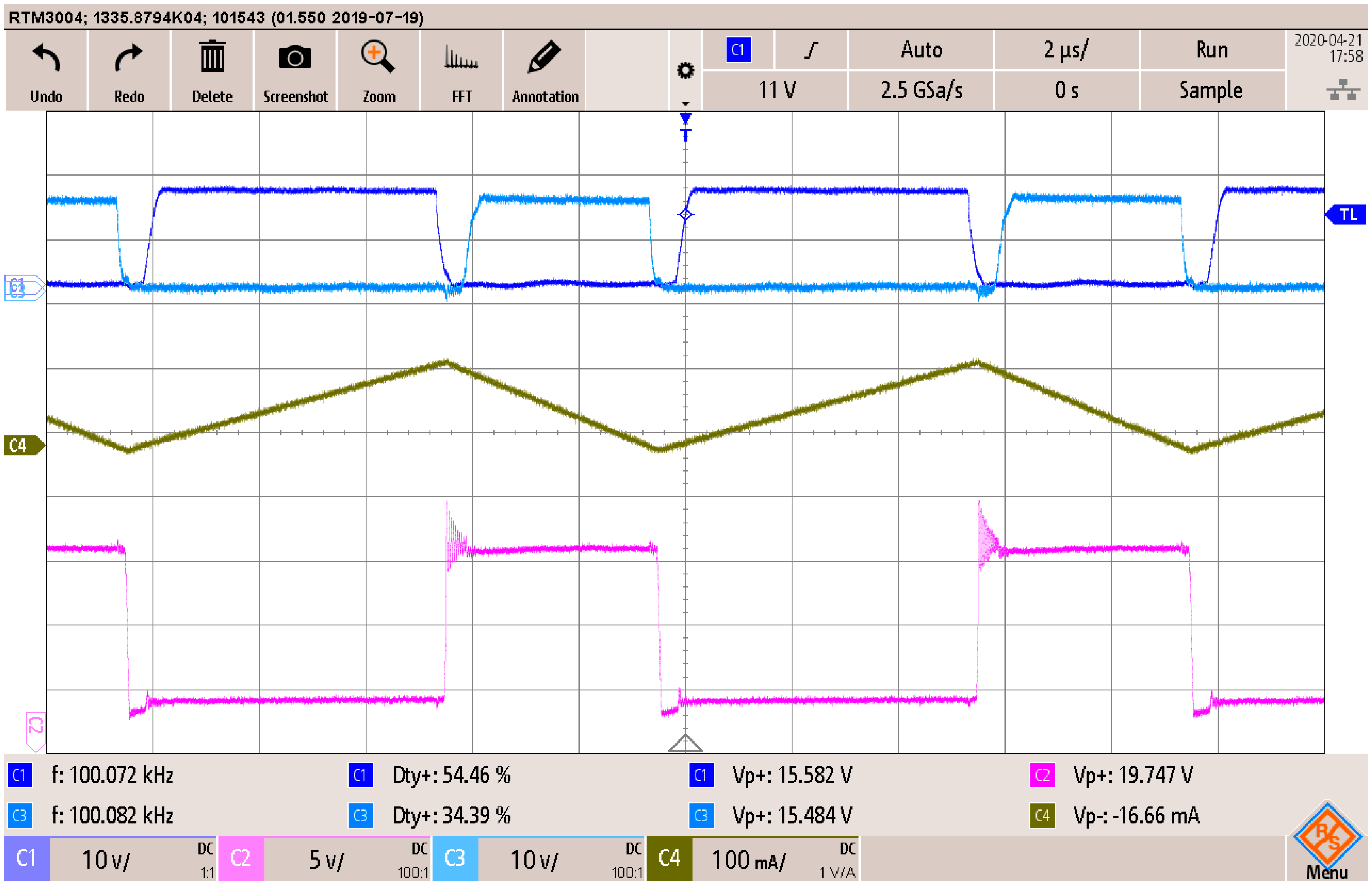
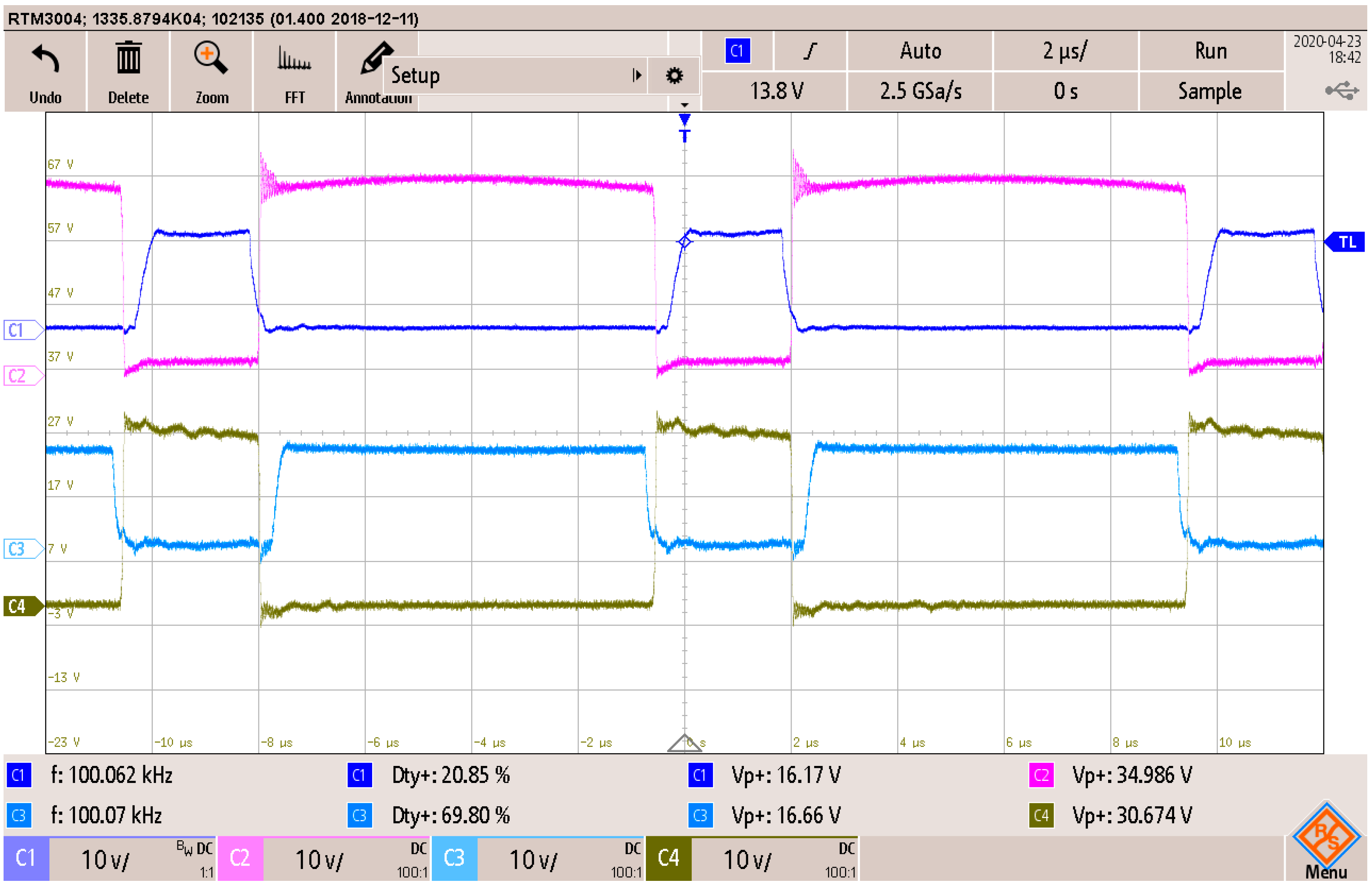
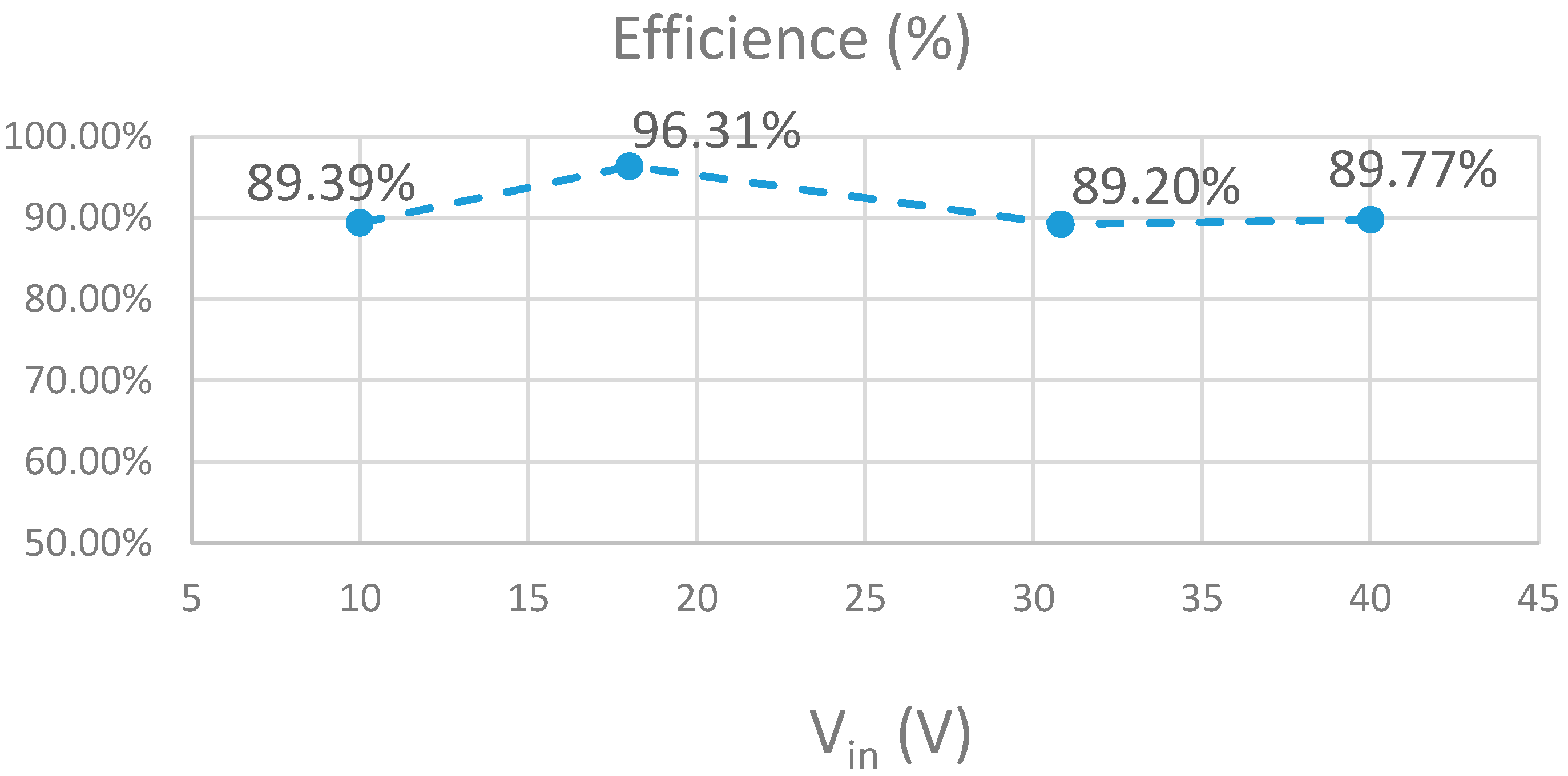
5. Circuit Design Simulation and Measured Results
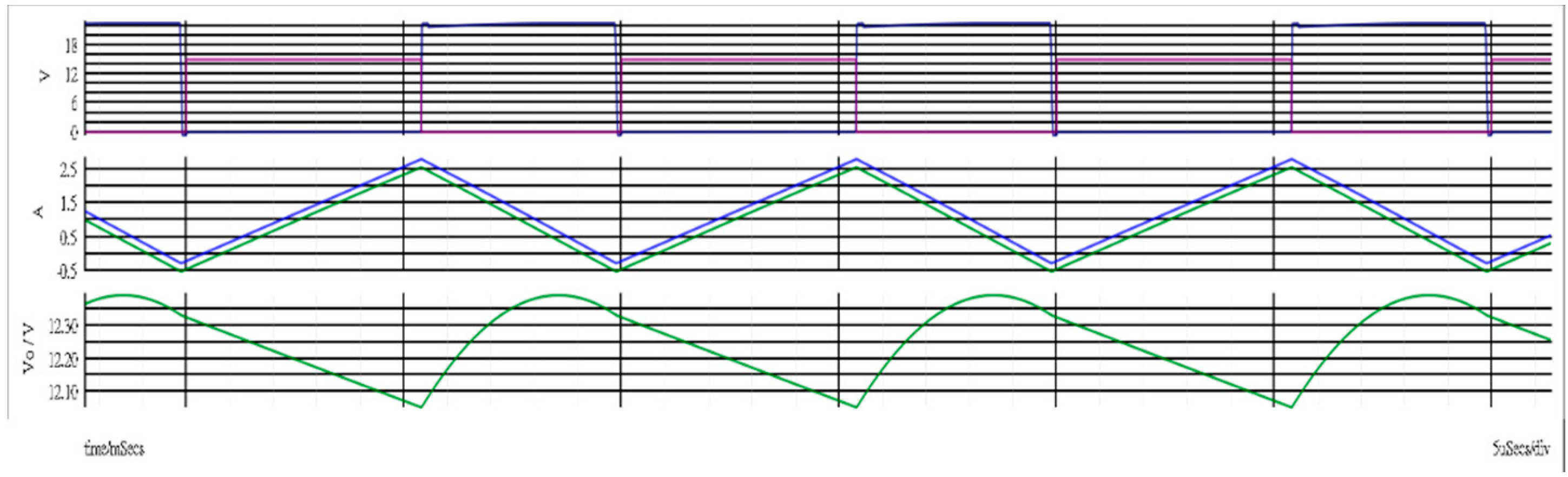
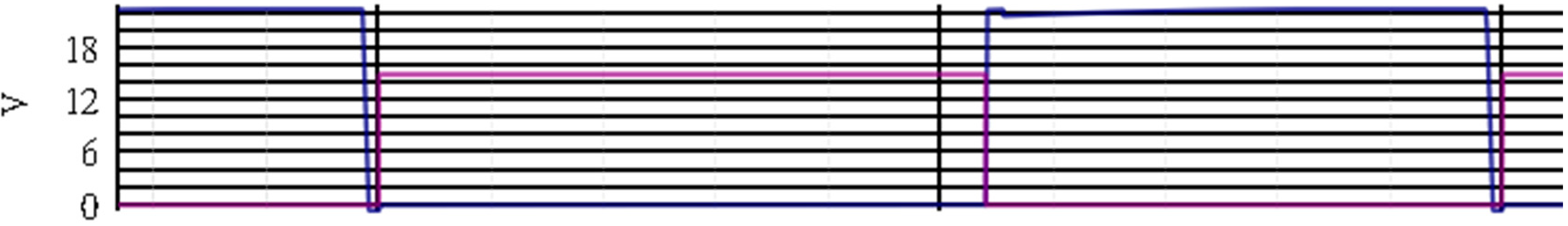
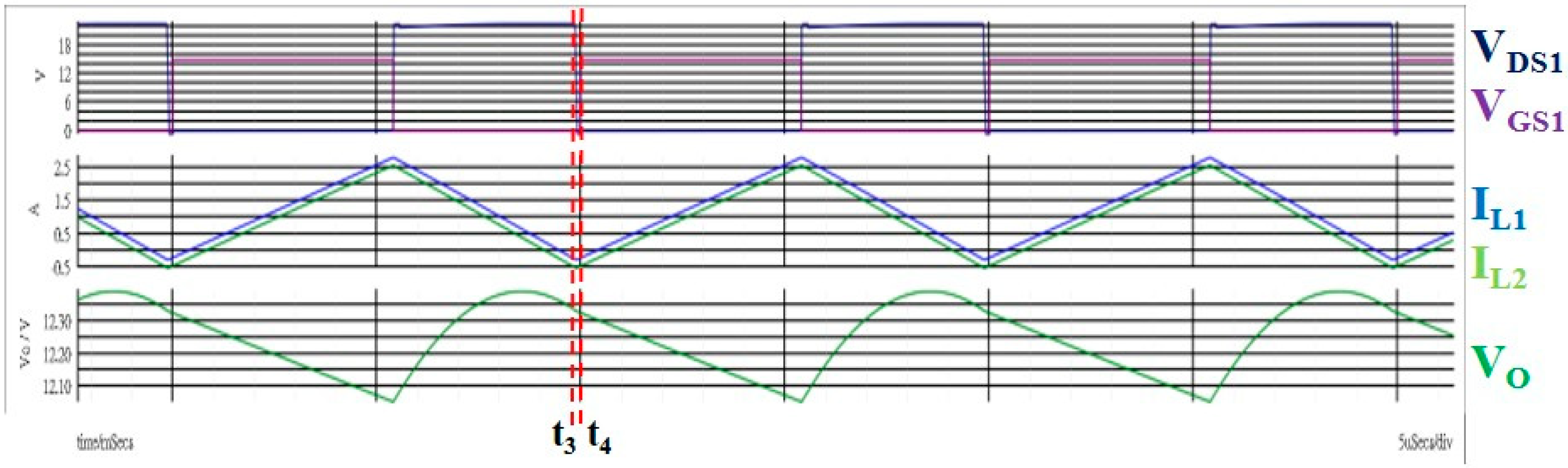
Measured Waveform
6. Conclusions
Author Contributions
Funding
Conflicts of Interest
References
- Technology Information ABC. Brief Description of the Characteristics of UIV OLED Lighting Source, Understand the Different Light. Home Furnish. 2019. Available online: https://kknews.cc/home/3v9lng3.html (accessed on 26 October 2020).
- Xiong, S.Z.; Xie, W.L.; Zhao, Y.; Wang, J.S.; Liu, E.F.; Wu, C.Y. A Simple and Flexible driver for OLED. In Proceedings of the 5th Asian Symposium on Information Display, ASID’99, Hsinchu, Taiwan, 6 August 2002. [Google Scholar]
- Buso, D.; Bhosle, S.; Liu, Y.; Ternisien, M.; Renaud, C.; Chen, Y.M. OLED Electrical Equivalent Device for Driver Topology Design. IEEE Trans. Ind. Appl. 2014, 50, 1459–1468. [Google Scholar] [CrossRef]
- Jacobs, J.; Hente, D.; Waffenschmidt, E. Drivers for OLEDs. In Proceedings of the 2007 IEEE Industry Applications Annual Meeting, New Orleans, LA, USA, 23–27 September 2007. [Google Scholar]
- Bęczkowski, S.; Munk-Nielsen, S. Led Spectral and Power Characteristics under Hybrid Pwm/Am Dimming Strategy. In Proceedings of the 2010 IEEE Energy Conversion Congress and Exposition, Atlanta, GA, USA, 1 November 2010. [Google Scholar]
- Park, J.; Ban, T.; Choi, D. Organic LEDs Combined With Inorganic LEDs. J. Lightwave Technol. 2011, 29, 2684–2689. [Google Scholar] [CrossRef]
- Le Minh, H.; Ghassemlooy, Z.; Burton, A.; Haigh, P.A. Equalization for organic light emitting diodes in visible light communications. In Proceedings of the 2011 IEEE GC Wkshps, Houston, TX, USA, 5–9 December 2011. [Google Scholar]
- Han, R.; Yang, C.C.; Chen, X.; Han, X.Q.; Zhang, J.; Li, C.N. Design of an Intelligent White-OLED Lighting System using Power Line Communication. In Proceedings of the 2012 2nd International CECNet, Yichang, China, 21–23 April 2012. [Google Scholar]
- Liu, Y.; Chen, Y.M.; Buso, D.; Zissis, G. Influence of Driving Current on Photometric Performances of a White Light OLED. IEEE Trans. Ind. Appl. 2016, 52, 5219–5225. [Google Scholar] [CrossRef]
- Wu, Y.-L. Switching Power Supply Converter for Principle and Practical Design; Wen-Sheng Publisher: Taipei, Taiwan, 2015. [Google Scholar]
- Falin, J. Designing DC/DC converters based on SEPIC topology. Analog Appl. J. 2018, 18–26. [Google Scholar]
- Verma, M.; Kumar, S.S. Hardware Design of SEPIC Converter and its Analysis. In Proceedings of the International Conference on Current Trends towards Converging Technologies (ICCTCT), Coimbatore, India, 1–3 March 2018. [Google Scholar]


| Item | Value |
|---|---|
| Input voltage | 10–40 V |
| Output voltage | 12 V/1 A |
| Switching frequency | 100 kHz |
| Frequency Conversion | 70–100 kHz |
| Component | Specification |
|---|---|
| MOSFET | IRF 2907Z (VDS = 75 V, RDS(on) = 4.5 mΩ) |
| Current Sensor | HX-10P |
| Inductors | 18 μH |
| Gate driver | HCPL-3120 |
| Vin | Vout | Efficiency | ||||
|---|---|---|---|---|---|---|
| V | A | P | V | A | P | |
| 9.9972 | 1.3795 | 13.79114 | 12.328 | 1 | 12.328 | 89.39% |
| 18.003 | 0.711 | 12.80013 | 12.328 | 1 | 12.328 | 96.31% |
| 30.816 | 0.4483 | 13.81481 | 12 | 1.0269 | 12.3228 | 89.20% |
| 40.022 | 0.339 | 13.56746 | 12.18 | 1 | 12.18 | 89.77% |
Publisher’s Note: MDPI stays neutral with regard to jurisdictional claims in published maps and institutional affiliations. |
© 2020 by the authors. Licensee MDPI, Basel, Switzerland. This article is an open access article distributed under the terms and conditions of the Creative Commons Attribution (CC BY) license (http://creativecommons.org/licenses/by/4.0/).
Share and Cite
Lin, Z.-R.; Chiu, H.-J. Design and Implementation of Solar OLED Lighting Driver Circuit with Frequency Modulation Control. Energies 2020, 13, 5608. https://doi.org/10.3390/en13215608
Lin Z-R, Chiu H-J. Design and Implementation of Solar OLED Lighting Driver Circuit with Frequency Modulation Control. Energies. 2020; 13(21):5608. https://doi.org/10.3390/en13215608
Chicago/Turabian StyleLin, Zhong-Rong, and Huang-Jen Chiu. 2020. "Design and Implementation of Solar OLED Lighting Driver Circuit with Frequency Modulation Control" Energies 13, no. 21: 5608. https://doi.org/10.3390/en13215608
APA StyleLin, Z.-R., & Chiu, H.-J. (2020). Design and Implementation of Solar OLED Lighting Driver Circuit with Frequency Modulation Control. Energies, 13(21), 5608. https://doi.org/10.3390/en13215608