Abstract
The aim of this paper is to present the real-time implementation and measurements of a reduced switch count in space vector pulse width modulation for three-level neutral point clamped inverters (3L-NPC). We implement space vector pulse width modulation, which uses a prediction algorithm to reduce the number of switches in power transistors (switch count) by up to about 13%. The algorithm applies additional redundant voltage vectors. The method is compute-intensive and was implemented on a dual-core TMS320F28379D digital signal controller. The latest measurements of steady and dynamic states of electric drive, powered by a 3L-NPC inverter using this method, confirmed the possibility of using this method in practical implementation. The implementation and results of the measurements are presented in this paper.
1. Introduction
The efficiency of power inverters depends mainly on power losses in semiconductor devices. These losses are the sum of conduction losses and switching losses [1,2]. Conduction losses depend on parameters of semiconductor devices and are not in the scope of this paper. Switching losses occur when turning the devices on or off. This paper presents a method of modified symmetric Space Vector Modulation (SVM or SVPWM) with switch count reduction (the number of individual switching in power transistors) in a three-level neutral point clamped inverter (3L-NPC). The method uses additional redundant voltage vectors in a way that reduces switch count by up to 20%. In the practical implementation presented in this paper, the switch count was reduced by 13.07% in the steady state. A reduction in the switch count increases efficiency, and as a result, it lowers the thermal load in switching devices, which can be very useful in the thermal design of medium- and high-power inverters [3]. In the presented method, an increase in efficiency depends on construction, switching devices, voltages, currents, load, and switching frequency of inverter [3].
The theoretical foundations for the switch count reduction method, first shown in [4], were based on simulations. The proof of concept for this method of modulation was presented in [5], but without the real-time implementation. However, due to a lack of sufficient computing power of the microcontroller used in [5], only static states with a limited temporal resolution could be observed. The next step of the implementation was to overcome and compute the intensive nature of this kind of modulation method by using a dual-core TMS320F28379D digital signal controller (DSC), which was presented in [6].
There are alternative ways to reduce the switch count. One is to alter the three-level inverter topology to reduce number of switching transistors, as in [7], but the downside of this is the need for six independent power supplies. Another approach would be to use a smaller number of voltage vectors in sampling the time, yet this reduces the quality of output current and requires additional measures to ensure proper neutral point balancing [8]. The most obvious way to decrease the switch count would be to use a smaller PWM frequency. However, this leads to higher THD. In contrast to the alternative methods mentioned above, the method presented in this paper by its nature virtually does not change the voltage waveforms at the output of the inverter. The modified switching sequence, which reduces the switch count, is obtained in software only and does not use phase current detection.
This paper presents measurements and a description of the switch reduction modulation method for the 3L-NPC inverter, which is now fully implemented in real-time and tested on the prototype inverter. The method, the measurement results, and the practical implementation are all presented in this paper.
The idea behind improving the modulation method for 3L-NPC was inspired by an increasing use of this type of multilevel inverter. This type of inverter is used mainly for medium and high voltages, as its topology allows the halving of the voltage rating of main components. 3L-NPC offers lower harmonic distortions, better efficiency, and lower stress on the isolation of motor windings [9]. 3L-NPC inverters have been recently studied and used in active power filters, industrial electric motor drives, and even in high power audio amplification [9,10,11].
2. Methods
A three-phase three-level neutral point clamped inverter consists of twelve transistors used as switches and has nineteen distinct phase-to-phase voltages [12]. The inverter used in this research is a prototype, which was custom made for the purpose of this research. The main circuit of the inverter is shown in Figure 1; a detailed description of the used inverter is presented in Appendix A.
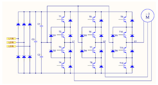
Figure 1.
The main circuit of the prototype three-level neutral point clamped (3L-NPC) inverter. T1–T12 are the IGBT transistors, D1–D6 are the neutral point clamping diodes, C1–C3 are the filtering capacitors, L1–L3 are input and output of the inverter, and M is the 3-phase squirrel cage induction motor.
Nineteen-output phase-to-phase voltage vectors can be represented in complex αβ space, which is used to implement a space vector modulation [9,13]. The representation of all output phase-to-phase voltages of 3L-NPC is presented in Figure 2. This gives 19 possible switching vectors used to synthesize the rotating U0 vector. U0 is a reference voltage vector and represents a rotating magnetic field. U0 is approximated as a weighted average combination of three adjacent switching voltage vectors [9,13,14].
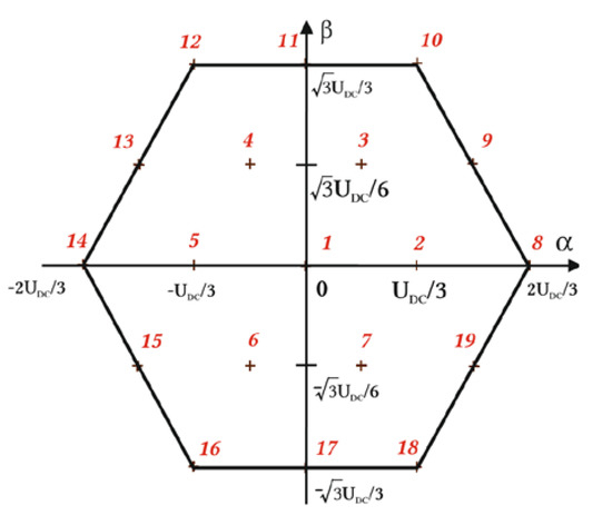
Figure 2.
Nineteen-output space vectors of the three-phase 3L-NPC inverter represented in αβ complex space, forming a regular hexagon. UDC is the rail-to-rail DC voltage at the inverter input.
2.1. Additional Redundant Voltage Vectors of 3L-NPC Inverter
It is commonly assumed that the 3L-NPC inverter has 33 = 27 switching states, which produce 19 vectors [14]. The number of switching states is the number of all combinations of phase leg voltages, and some of them give two or three redundant vectors. This fact is used to create optimized switching sequence to avoid excessive switching [14]. This assumption is based on the fact that every phase leg of 3L-NPC has three voltage states. For example, if transistors T1 and T2 are switched on, the full UDC is present at the output of the first phase leg. Similarly, if T2 and T3 are switched on, the voltage is UDC/2; then, for T3 and T4 the voltage is 0 [10,12,14].
As presented in Figure 3, it can be proven that considering current flows in the inverter circuit in a way to avoid short circuit, it is possible to turn on only one transistor in a phase leg in a three-phase 3L-NPC and that gives UDC/2 in a three-phase 3L-NPC leg. This gives additional redundant vectors, which can be used to further optimize the switching sequence and thus, reduce the switch count. All switching states used in this research are presented in Table 1. The switching optimization is not fixed but it is calculated in real-time, considering the two next space vectors in a vector sequence that are needed to obtain a reference vector U0.
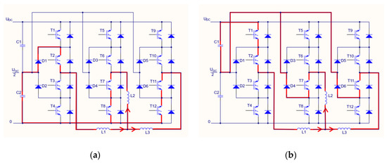
Figure 3.
An example of the current flow in the 3L-NPC inverter for the space vector number 2 (Figure 2): (a) a redundant vector which draws the current from C2; (b) a redundant vector which draws the current from C1.

Table 1.
The switching states of the 3L-NPC inverter corresponding to the voltage vectors.
2.2. Space Vector Modulation with a Reduced Switch Count
We implement the method using modified SVM that utilizes the additional redundant vectors to synthesize the U0 reference voltage vector. A detailed flowchart for this method is presented in Figure 4.
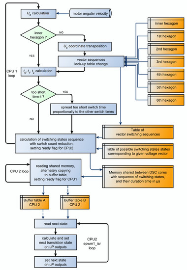
Figure 4.
The flowchart of the switch count reduction method implemented on a dual-core DSC.
Assuming that the sampling time TC is constant and sufficiently small, the U0 is considered constant in that time. U0 is approximated as a weighted average combination of three adjacent switching voltage vectors, as in a two-level inverter, as shown in Figure 5 [9,13,14]. Equations (1) and (2) are used to calculate the switching time of the ith vector adjacent to U0, within one sampling period TC.
TCU0(ω0t) = t1Uwi + t2Uw(i+1),
t0 = TC − t1 − t2,
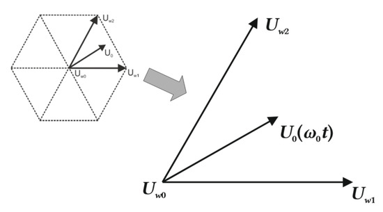
Figure 5.
The U0 reference voltage vector approximated as a weighted average combination of three adjacent switching voltage vectors as in the two-level inverter.
The calculated times t0, t1, and t2 are then used with the corresponding voltage vectors in a symmetric PWM switching sequence (t0/4, t1/2, t2/2, t0/2, t2/2, t1/2, t0/4) to minimize the THD [14]. In case of the first sector of a two-level hexagon (as in Figure 4), the calculated times correspond to Uw0, Uw1, and Uw2, while the switching sequence over one sampling period TC is: Uw0, Uw1, Uw2, Uw0, Uw2, Uw1, and Uw0. All used sequences of the voltage vectors are presented in Appendix B.
2.2.1. Decomposition of a Three-Level Hexagon
For quick two-level calculations in 3L-NPC, we use the decomposition method from [14], where the U0 vector coordinates are transposed to one of six outer hexagons, as shown in Figure 6. The transposition is used if the U0 length is greater than half of the full modulation index (the inner circle in Figure 5). The decision to which outer hexagon U0 should be transposed depends on the U0 angle in the polar coordinates: −π/6 to π/6 is the 1st outer hexagon; π/6 to π/2 is the 2nd outer hexagon, etc.
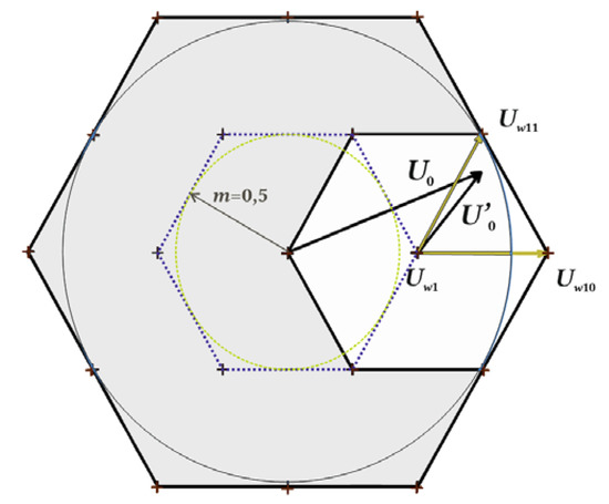
Figure 6.
The transposition of the U0 reference voltage vector coordinates to the first outer hexagons out of six.
After the transposition of U0 to U’0, the table of the voltage vector sequence which corresponds to the chosen outer hexagon is set. In the case shown in Figure 6, U’0 is in the first sector of the first outer hexagon and the sequence of vectors is: Uw1, Uw10, Uw11, Uw1, Uw11, Uw10, and Uw1 (the first row in Table A3).
2.2.2. Switch Count Reduction
The current state of 12 transistors is compared with redundant switching states corresponding to the next voltage vector in the switching sequence, to find one with the smallest possible changes in the conducting state of the transistors. This is done by a bitwise XOR operation on the current and following state. Next, the number of “ones” is counted for each possibility that designates the number of individual transistor state changes. In the example shown in Table 2, the second and the fourth row show only two changes.
Table 2.
Example of determining the next redundant switching state in the vector sequence.
The search for the most optimal switching sequence is carried out for two steps ahead in the vector sequence, to further enhance the reduction in the switch count. Simulations show that an increase in the number of steps above two does not improve the effectiveness of this method [4].
The maximum effectiveness of the switch count reduction method is mainly dependent on the modulation index. The effectiveness rises from one half of the full modulation. It is at its highest point at full modulation, where this method reduces switch count, up to 20%. There is no improvement under one half of the full modulation [5]. The sampling time TC and the output voltage frequency also have an impact on the effectiveness of the reduction in the switch count. The chosen neutral point voltage balancing method has a major impact on the effectiveness of the reduction in the switch count. This is because it requires a temporary reduction in the selection of the optimal switching sequence. In the presented implementation, the switch count reduction is lower due to the factors mentioned above.
2.3. Highlights of the Hardware Implementation
The novel approach of the switch count reduction method requires a custom implementation. The method was implemented on a TMS320F28379D digital signal controller [6].
The dual-core implementation highlights:
- The first core is designed to control the U0 vector, calculate SVM switching times, and optimize the switching sequence to reduce the switch count. The calculated switching vector sequence, together with the appropriate switching times, are sent to the second core.
- The second core is used to set twelve PWM outputs with 1μs temporal resolution, according to the calculated switching times and sequence, with consideration of dead-band time. Six ePWM DSC modules with twelve high resolution outputs, ePWM1 to ePWM6, are synchronized together. The PWM output state is forced through the software control at the end of each 1μs PWM period. Every one microsecond epwm1_isr interrupt function is called to set outputs in line with the two n × 2 integer array computed by the first core. The array is sent alternately to two data tables of the second core, through shared RAM. Two data tables are used to avoid data starvation. The alternate calculated SVM data flow is depicted in Figure 4 by dashed and solid lines.
2.4. Temporal Resolution, Timing, and Dead-Band Time
The sampling period of the SVM was set to TC = 500 μs (2 kHz sampling frequency) in this research. The temporal resolution tr = 1 μs was chosen, as it was found to be the smallest practical amount of time in which twelve PWM outputs of TMS320F28379D DSC can be arbitrarily set and synchronized together [6]. As a result, every calculated switching time is rounded to 1 μs.
Dead-band time is set to td = 4 µs. Dead band is the time needed for a transistor to change its conducting state, to avoid a simultaneous conduction of three or four transistors in one phase leg, thus causing short circuit. The minimum calculated switching time for any voltage vector is set to tn = 10 µs, which gives a minimum of 6 µs of the active switching time, as shown in Figure 7d. Any calculated switching time tn that is shorter than 10 µs is discarded and spread proportionally to the other two switching times calculated within the TC sampling period. This procedure will affect the PWM sequence in a way presented in Figure 7b. In the most extreme case, only one switching voltage vector is used within TC, as shown in Figure 7c. This method is not the only one to address this problem. To improve this method, it is possible, for instance, to offset that kind of rounding error in the following sampling periods.
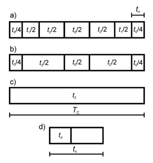
Figure 7.
Sequences of the switching voltage vectors in a sampling time TC. (a) A symmetric PWM switching sequence; (b) a sequence without Uw1 voltage vector; (c) Uw2 a voltage vector in the entire TC period; (d) the dead-band time td within one of the voltage vector switching times tn.
The dead-band transition switching state is effectively computed by the second core of DSC, as a bitwise AND of the current and the next switching state. This transition state ensures that all transistors, which were turned on in the previous state and will be turned off in the following state, have enough time to turn off. An example of that calculation is given in Table 3. In some cases, the transition state is equal to the next state, as can be seen in the second row of Table 3.
Table 3.
Example calculations of the dead-band transition switching states (T1-T12).
2.5. Neutral-Point Voltage Balancing
Voltage in the point between the C1 and C2 capacitors is called a neutral-point voltage (Figure 1). Fluctuation of the neutral-point voltage is a major problem to overcome in 3L-NPC inverters. This fluctuation is caused by uneven load of the C1 and C2 capacitors. There are many methods to maintain proper voltage balancing [9]. In 3L-NPC, there are six half-voltage switching voltage vectors Uw1 to Uw6 (Table 1). Each one of those vectors can be obtained by switching states loading C1 or C2 capacitors.
In the presented implementation, the duration of the switching state used to obtain vectors Uw1 to Uw6 is summed as positive or negative values for the C1 or C2 loading states. If the sum is lower than −200μs or larger than 200 μs, then the algorithm can use only those switching states that load the capacitor with higher voltage, until the duration difference is kept within ±200 μs.
The used method of neutral-point voltage balancing gave proper balancing for presented measurements. In more practical implementations, the neutral-point voltage is often measured during operation of the inverter and the modulation algorithm takes this measurement into account for voltage balancing. This approach will be used in future research.
3. Results
In this section, we compare measurements of the method implementation, with and without the use of additional redundant switching vectors. The aim of those measurements was to determine if the application of the method, under the normal use of the variable frequency drive, has an adverse impact on the output waveforms of the inverter, such as the efficiency, THD levels, the levels of voltage and current, as well as other unforeseen implementation difficulties.
The measurements were carried out using the following equipment:
- A prototype inverter, as described in Appendix A;
- The National Instruments PXIe-1062Q (with two PXI-6133 and two BNC-2120 modules) for the data acquisition;
- Two differential amplifiers (PE-5310-2B) for the purpose of the measuring of the output voltage;
- Six LEM 50 A/0.5 V current probes, for measuring the input and output current;
- A Lucas-Nuelle SE2672-3G three-phase squirrel-cage induction motor;
- SICK DFS60B-S4PA10000 incremental encoder.
The SVM parameters were described in Section 2.4. For the measurements, we chose delta connection. The voltage on the filtering capacitor UDC was set to 480 V. The motor was loaded with a 1.02 Nm torque during the steady state tests. The angular velocity measurement is taken every 20 ms. The PI regulator was implemented with the following coefficients: Kp = 0.3413, Ki = 12.4562. The coefficients were obtained with the Cohen–Coon tuning method. The goal of the regulator was to maintain the angular velocity of the motor at 3000 rpm for 10 s per measurement. The V/f control is used. Measurements are shown in Figure 8, Figure 9, Figure 10, Figure 11, Figure 12, Figure 13, Figure 14, Figure 15, Figure 16, Figure 17, Figure 18, Figure 19, Figure 20 and Figure 21. The figures show voltages and currents from t = 2 to 2.05 s.
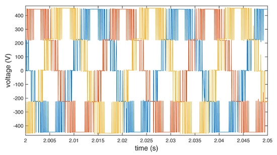
Figure 8.
Output line to line voltage of the inverter using standard redundant switching vectors.
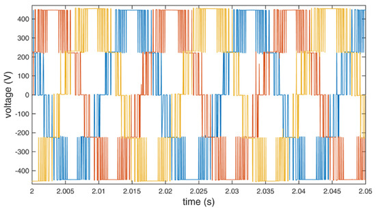
Figure 9.
Output line to line voltage of the inverter using additional redundant switching vectors.
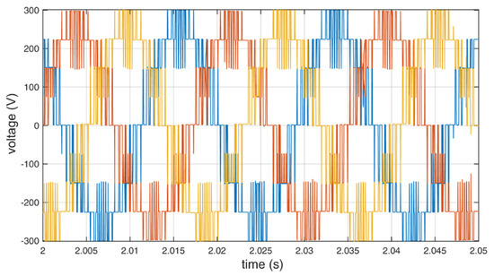
Figure 10.
Output line to neutral voltage of the inverter using standard redundant switching vectors.
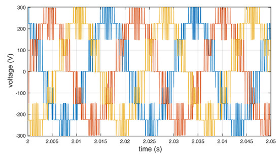
Figure 11.
Output line to neutral voltage of the inverter using additional redundant switching vectors.
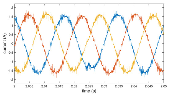
Figure 12.
Line currents of the motor using standard redundant switching vectors.
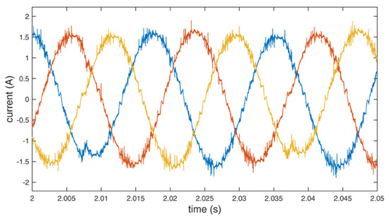
Figure 13.
Line currents of the motor using additional redundant switching vectors.
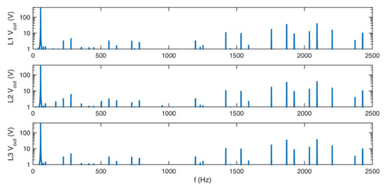
Figure 14.
Frequency spectra of the output voltages for standard redundant switching vectors.
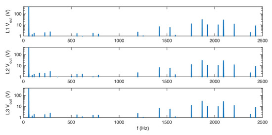
Figure 15.
Frequency spectra of the output voltages for additional redundant switching vectors.
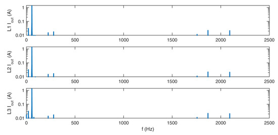
Figure 16.
Frequency spectra of the output currents for standard redundant switching vectors.
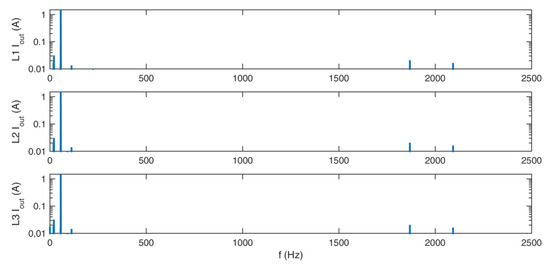
Figure 17.
Frequency spectra of the output currents for additional redundant switching vectors.
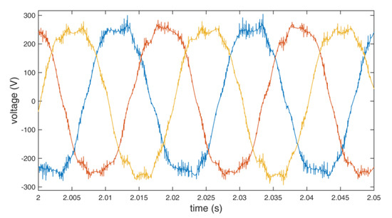
Figure 18.
Input line to neutral voltage of the inverter using standard redundant switching vectors.
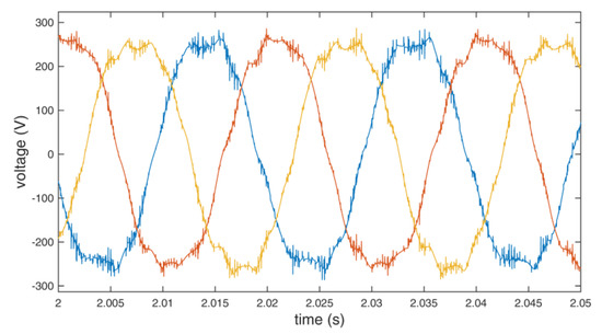
Figure 19.
Input line to neutral voltage of the inverter using additional redundant switching vectors.
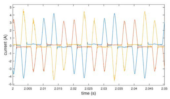
Figure 20.
Input line current of the inverter using standard redundant switching vectors.
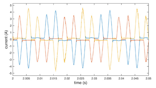
Figure 21.
Input line current of the inverter using additional redundant switching vectors.
The collected data were analyzed for differences between the use of the standard and the additional redundant switching vectors. In both cases, the inverter maintained the mean frequency at 56.0 Hz to overcome the torque and maintain 3000 rpm. Although a significant reduction in the switch count is obtained (up to about 13% in the presented implementation), there is no substantial impact on the waveforms. The output level of voltages and currents are similar in both cases. Theoretical power efficiency gain cannot be confirmed with the used measurement setup because its level is below the border of the measuring error. Nevertheless, the efficiency gains can be calculated, depending on the construction, the switching devices, voltages, currents, load, and switching frequency of the used inverter [1,2,3]. The efficiency gains would be more pronounced if a significantly larger motor were used.
Figure 14, Figure 15, Figure 16 and Figure 17 show the frequency spectra of the output voltages and currents. The main peak on those figures is the first harmonic. Around 2 kHz, harmonics of the chosen sampling frequency TC can be seen, which are the characteristics of the SVM. The THD is relatively low in both cases, with and without the use of additional redundant switching vectors, as shown in Table 4.
Table 4.
THD levels of output voltages and currents, for standard and additional redundant switching vectors.
The dynamic state of the drive was measured with the voltage on the filtering capacitor UDC set to 400 V. The motor was not loaded. The other parameters were set as in the steady state measurements. The set value of speed over time and the measured value are shown in Figure 22. The red curve in Figure 22 shows the set angular velocity over time, and the blue one is the angular velocity of the motor. After comparing these curves, one can conclude that the implementation of the PI control provides a quick response of the angular velocity. In the first half of the time, the standard switching vectors are used. In the second half, the standard and additional redundant switching vectors are used. The voltages and currents are shown in Figure 23, Figure 24, Figure 25 and Figure 26.
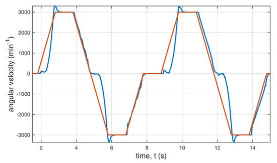
Figure 22.
Angular velocity of the motor over time with the set velocity in red and the measured velocity in blue.
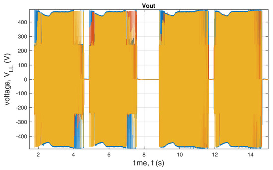
Figure 23.
Output voltage of the inverter during the dynamic state.
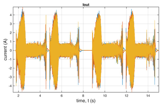
Figure 24.
Output current of the inverter during the dynamic state.
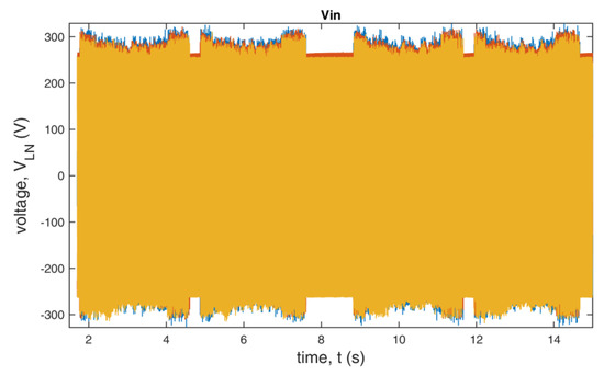
Figure 25.
Input voltage of the inverter during the dynamic state.
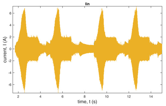
Figure 26.
Input current of the inverter during the dynamic state.
We analyzed the data during dynamic state also for differences between the use of standard and additional redundant switching vectors. The example presented in Figure 23, Figure 24, Figure 25 and Figure 26 shows that there are minor changes in output voltages and currents during the dynamic state, especially at the time of slowing down of the drive.
The exact number of times the switching is conducted vary slightly between measurements, because of the nature of closed loop control of the real object. For this reason, the presented switch count reduction values are obtained from the algorithm simulation. In steady states, with full modulation index, 56 Hz output frequency, during 10 s of operation, the reduction in the switch count is 13.07%. In the dynamic state, with the desired velocity curve depicted by a red line in Figure 22, there is a reduction in the switch count of 6.43%. The switch count for presented measurement examples is shown in Table 5.
Table 5.
Switch count reduction switching vectors.
4. Discussion and Conclusions
Based on mathematical methods and measurements, we conclude that it is possible to utilize the additional redundant voltage vectors in the switching sequence. As the measurements results show, the method of reducing switch count in a three-level NPC inverter can be used in a drive with an induction motor, without a significant deterioration of the output waveforms of the inverter. In tested cases, it was found that the THD levels were slightly higher, when the switch count reduction method was used. In the steady state practical implementation, the switch count was reduced by 13.07%, which is a quite good value. It is worth mentioning that the implementation on a TMS320F28379D DSC did not use all its computing power. The core that computes the SVM sequence and PI control is used in about 30%, which can and will be used in further research to implement the control scheme for an active power filter. The second core’s computing power, which sets the twelve outputs in 1 µs time resolution, is used almost completely.
In order for a reduction in the switch count to be possible in real-time, we applied the following methods: parallel computing, space vector pulse width modulation, decomposition of a three-level hexagon, determining of the most optimal switching sequence, and neutral-point voltage balancing based only on the conducting time of the transistors and the PI control.
The method can be useful as one of the means to lower the thermal load on switching devices. The power efficiency gain of the method is expected to be more prominent in medium- and high-power applications. The presented method can be implemented without changing the electrical structure of the inverter. Although the method is demanding computationally, it can be implemented on a relatively low-cost digital signal controller.
Author Contributions
Conceptualization, K.R. and R.B.; methodology, R.B.; software, K.R. and K.G.; validation, R.B.; formal analysis, R.B. and K.R.; investigation, R.B., K.G., K.R. and P.P.; resources, K.G. and P.P.; data curation, R.B. and K.R.; writing—original draft preparation, K.R.; writing—review and editing, R.B. and K.G.; visualization, K.R.; supervision, R.B.; project administration, R.B.; funding acquisition, R.B. All authors have read and agreed to the published version of the manuscript.
Funding
This research received no external funding.
Acknowledgments
We would like to thank Patrycja Beniak for all hervaluable assistance with proofreading the paper. We also like to thank Rudolf Staisz for technical support during measurements.
Conflicts of Interest
The authors declare no conflict of interest.
Appendix A
A prototype inverter used in this research was custom built. The method presented in this paper could not be implemented on any system available to the authors. The key feature of the presented inverter is the ability to control all 12 transistors independently. The list of main components is shown in Table A1. Figure A1 presents IGBT modules mounted on a radiator. Figure A2 presents the daughter board converting logic levels, mounted on a TMS320F28379D evaluation board.
Table A1.
List of main components of the prototype inverter.
Table A1.
List of main components of the prototype inverter.
| Component | Name | Features |
|---|---|---|
| IGBT modules | Infineon FS150R12KE3G | 6 IGBT transistors (VCE = 1200 V, ICnom = 150 A) and six clamping diodes (VRRM = 1200 V, IF = 150 A) |
| NPC diodes | IXYS Dsei2 × 101-12a | VRRM = 1200 V, IF = 99 A |
| Filtering capacitors | Kemet ALS70A332MF500 | 4 × 3300 µF, 500 V |
| Bridge rectifier | Vishay VS-90MT120KPBF | VRRM = 1200 V, IO = 90 A, IFSM = 770 A |
| IGBT control modules | Infineon 6ED100E12-F2 | Dedicated evaluation driver board |
| Daughter board (Figure A2) | custom | Converting 3.3 V logic to 5 V for PWM 12 outputs 4 inputs from speed encoder 14 analog inputs for future use |
| Digital Signal Controller (Figure A2) | TMS320F28379D | Texas Instruments launch pad |
| Voltage surge protector | custom | IGBT crowbar circuit |
| Power supply | custom | 3.3 V; 5 V; −15 V; 15 V |

Figure A1.
Prototype inverter (during assembly)—IGBT modules with driver boards are on the left; power supply modules are on the right.
Figure A1.
Prototype inverter (during assembly)—IGBT modules with driver boards are on the left; power supply modules are on the right.


Figure A2.
Digital Signal Controller TMS320F28379D launch pad with daughter board.
Figure A2.
Digital Signal Controller TMS320F28379D launch pad with daughter board.

Appendix B
The tables of voltage vector sequences, corresponding to the chosen outer hexagon, used in the decomposition method, are shown in Table A2, Table A3, Table A4, Table A5, Table A6, Table A7 and Table A8.
Table A2.
Voltage vector switching sequences of the inner hexagon, by ith vector designation (Uwi).
Table A2.
Voltage vector switching sequences of the inner hexagon, by ith vector designation (Uwi).
| Sector | Vector Sequence |
|---|---|
| 1 | 0, 1, 2, 0, 2, 1, 0 |
| 2 | 0, 3, 2, 0, 2, 3, 0 |
| 3 | 0, 3, 4, 0, 4, 3, 0 |
| 4 | 0, 5, 4, 0, 4, 5, 0 |
| 5 | 0, 5, 6, 0, 6, 5, 0 |
| 6 | 0, 1, 6, 0, 6, 1, 0 |
Table A3.
Voltage vector switching sequences of the 1st outer hexagon, by ith vector designation (Uwi).
Table A3.
Voltage vector switching sequences of the 1st outer hexagon, by ith vector designation (Uwi).
| Sector | Vector Sequence |
|---|---|
| 1 | 1, 10, 11, 1, 11, 10, 1 |
| 2 | 1, 2, 11, 1, 11, 2, 1 |
| 3 | 1, 2, 0, 1, 0, 2, 1 |
| 4 | 1, 6, 0, 1, 0, 6, 1 |
| 5 | 1, 6, 21, 1, 21, 6, 1 |
| 6 | 1, 10, 21, 1, 21, 10, 1 |
Table A4.
Voltage vector switching sequences of the 2nd outer hexagon, by ith vector designation (Uwi).
Table A4.
Voltage vector switching sequences of the 2nd outer hexagon, by ith vector designation (Uwi).
| Sector | Vector Sequence |
|---|---|
| 1 | 2, 11, 12, 2, 12, 11, 2 |
| 2 | 2, 13, 12, 2, 12, 13, 2 |
| 3 | 2, 13, 3, 2, 3, 13, 2 |
| 4 | 2, 0, 3, 2, 3, 0, 2 |
| 5 | 2, 0, 1, 2, 1, 0, 2 |
| 6 | 2, 11, 1, 2, 1, 11, 2 |
Table A5.
Voltage vector switching sequences of the 3rd outer hexagon, by ith vector designation (Uwi).
Table A5.
Voltage vector switching sequences of the 3rd outer hexagon, by ith vector designation (Uwi).
| Sector | Vector Sequence |
|---|---|
| 1 | 3, 2, 13, 3, 13, 2, 3 |
| 2 | 3, 14, 13, 3, 13, 14, 3 |
| 3 | 3, 14, 15, 3, 15, 14, 3 |
| 4 | 3, 4, 15, 3, 15, 4, 3 |
| 5 | 3, 4, 0, 3, 0, 4, 3 |
| 6 | 3, 2, 0, 3, 0, 2, 3 |
Table A6.
Voltage vector switching sequences of the 4th outer hexagon, by ith vector designation (Uwi).
Table A6.
Voltage vector switching sequences of the 4th outer hexagon, by ith vector designation (Uwi).
| Sector | Vector Sequence |
|---|---|
| 1 | 4, 0, 3, 4, 3, 0, 4 |
| 2 | 4, 15, 3, 4, 3, 15, 4 |
| 3 | 4, 15, 16, 4, 16, 15, 4 |
| 4 | 4, 17, 16, 4, 16, 17, 4 |
| 5 | 4, 17, 5, 4, 5, 17, 4 |
| 6 | 4, 0, 5, 4, 5, 0, 4 |
Table A7.
Voltage vector switching sequences of the 5th outer hexagon, by ith vector designation (Uwi).
Table A7.
Voltage vector switching sequences of the 5th outer hexagon, by ith vector designation (Uwi).
| Sector | Vector Sequence |
|---|---|
| 1 | 5, 6, 0, 5, 0, 6, 5 |
| 2 | 5, 4, 0, 5, 0, 4, 5 |
| 3 | 5, 4, 17, 5, 17, 4, 5 |
| 4 | 5, 18, 17, 5, 17, 18, 5 |
| 5 | 5, 18, 19, 5, 19, 18, 5 |
| 6 | 5, 6, 19, 5, 19, 6, 5 |
Table A8.
Voltage vector switching sequences of the 6th outer hexagon, by ith vector designation (Uwi).
Table A8.
Voltage vector switching sequences of the 6th outer hexagon, by ith vector designation (Uwi).
| Sector | Vector Sequence |
|---|---|
| 1 | 6, 21, 1, 6, 1, 21, 6 |
| 2 | 6, 0, 1, 6, 1, 0, 6 |
| 3 | 6, 0, 5, 6, 5, 0, 6 |
| 4 | 6, 19, 5, 6, 5, 19, 6 |
| 5 | 6, 19, 20, 6, 20, 19, 6 |
| 6 | 6, 21, 20, 6, 20, 21, 6 |
References
- Feix, G.; Dieckerhoff, S.; Allmeling, J.; Schonberger, J. Simple Methods to Calculate IGBT and Diode Conduction and Switching Losses. In Proceedings of the 13th European Conference on Power Electronics and Applications, Barcelona, Spain, 8–10 September 2009. [Google Scholar]
- Drofenik, U.; Kolar, J.W. A General Scheme for Calculating Switching- and Conduction-Losses. In Proceedings of the 5th International Power Electronics Conference, IPEC, Niigata, Japan, 4–8 April 2005. [Google Scholar]
- Mazgaj, W.; Rozegnał, B.; Szular, Z. Switching losses in three-phase voltage source inverters. Elektrotechnika 2015, 2-E, 47–60. [Google Scholar] [CrossRef]
- Beniak, R.; Rogowski, K. A method of reducing switching losses in three-level NPC inverter. Power Electron. Drives 2016, 1, 55–63. [Google Scholar] [CrossRef]
- Beniak, R.; Rogowski, K. A method of reducing switching losses in three-level NPC inverter—Analysis in steady states. Power Electron. Drives 2016, 2, 117–126. [Google Scholar] [CrossRef]
- Górecki, K.; Rogowski, K.; Beniak, R. Three-level NPC Inverter SVM Implementation on Delfino DSC. In Proceedings of the 16th IFAC Conference on Programmable Devices and Embedded Systems, High Tatras, Slovakia, 29–31 October 2019. [Google Scholar] [CrossRef]
- Salem, A.; Ahmed, E.M.; Ahmed, M.; Orabi, M.; Abdelghani, A.B. Reduced Switches Based Three-Phase Multi-Level Inverter for Grid Integration. In Proceedings of the 6th International Renewable Energy Congress (IREC), Sousse, Tunisia, 24–26 March 2015. [Google Scholar] [CrossRef]
- Kołomyjski, W.; Malinowski, M.; Kaźmierkowski, M.P. Adaptive Space Vector Modulator for Three-Level NPC PWM Inverter-Fed Induction Motor. In Proceedings of the 9th IEEE International Workshop on Advanced Motion Control, Istanbul, Turkey, 27–29 March 2006. [Google Scholar] [CrossRef]
- Kouro, S.; Malinowski, M.; Gopakumar, K.; Pou, J.; Franquelo, L.G.; Wu, B.; Rodríguez, J.; Pérez, M.A.; Leon, J.I. Recent Advances and Industrial Applications of Multilevel Converters. IEEE Trans. Ind. Electron. 2010, 57, 2553–2580. [Google Scholar] [CrossRef]
- Monroy-Morales, J.L.; Campos-Gaona, D.; Hernández-Ángeles, M.; Peña-Alzola, R.; Guardado-Zavala, J.L. An Active Power Filter Based on a Three-Level Inverter and 3D-SVPWM for Selective Harmonic and Reactive Compensation. Energies 2017, 10, 297. [Google Scholar] [CrossRef]
- Hoon, Y.; Mohd Radzi, M.A.; Hassan, M.K.; Mailah, N.F. A Dual-Function Instantaneous Power Theory for Operation of Three-Level Neutral-Point-Clamped Inverter-Based Shunt Active Power Filter. Energies 2018, 11, 1592. [Google Scholar] [CrossRef]
- Nabae, A.; Takahashi, I.; Hirofumi, A. A New Neutral-Point-Clamped PWM Inverter. IEEE Trans. Ind. Appl. 1981, IA-17, 518–523. [Google Scholar] [CrossRef]
- Van der Broeck, H.W.; Skudelny, H.-C.; Stanke, G.V. Analysis and realization of a pulsewidth modulator based on voltage space vectors. IEEE Trans. Ind. Appl. 1988, 24, 142–150. [Google Scholar] [CrossRef]
- Holmes, D.G.; Lipo, T.A. Pulse width Modulation for Power Converters: Principles and Practice; IEEE Press: Piscataway, NJ, USA, 2003. [Google Scholar]


Publisher’s Note: MDPI stays neutral with regard to jurisdictional claims in published maps and institutional affiliations. |
© 2020 by the authors. Licensee MDPI, Basel, Switzerland. This article is an open access article distributed under the terms and conditions of the Creative Commons Attribution (CC BY) license (http://creativecommons.org/licenses/by/4.0/).