Abstract
In this paper, a triangular spread-spectrum mechanism is proposed to suppress the electromagnetic interference (EMI) of a DC-DC buck converter. The proposed triangular spread-spectrum mechanism, which is implemented in the chip, can avoid modifying the printed circuit board of switching regulators. In addition, a lower ripple of output voltage of switching regulators and a better system stability can be realized by the inductive DC resistance (DCR) current sensing circuit. The chip is fabricated by using TSMC 0.18-μm 1P6M CMOS technology. The chip area including PADs is 1.2 × 1.15 mm2. The input voltage range is 2.7~3.3 V and the output voltage is 1.8 V. The maximum load current is 700 mA. The off-chip inductor and capacitor are 3.3 μH and 10 μF, respectively. The experimental results demonstrate that the maximum spur of the proposed DC-DC buck converter with the triangular spread-spectrum mechanism improves to 14dBm. Moreover, the transient recovery time of step-up and step-down loads are both 5 μs. The measured maximum efficiency is 94% when the load current is 200 mA.
1. Introduction
In recent years, portable electronic devices have become an indispensable necessity in daily life. Power management integrated circuits (PMICs) are widely used in portable electronic devices such as smart phones, tablets, laptops, and digital cameras. These products are constantly being updated to make them more practical and convenient. In general, fixed operating frequency control and variable operating frequency control are used in the switching regulator. Switching regulators with fixed operating frequency include both voltage mode control [1,2] and current control mode [3,4,5]. Fixed operating frequency control mechanisms must utilize an error amplifier and additional compensation components to stabilize the output voltage of the DC-DC buck converter. Another type of control scheme is variable operating frequency control, including hysteresis control [6,7,8] and constant on-time control [9,10,11]. First, the hysteresis control is controlled by the ripple of output voltage of the DC-DC buck converter. When the ripple of output voltage is higher than the upper threshold voltage or lower than the lower threshold voltage, the control circuit will generate a corresponding switching signal to drive power transistors. In addition, to stabilize the system it is necessary to use a capacitor with large equivalent series resistance (ESR) as an output capacitor of the DC-DC buck converter, such as an electrolytic capacitor. The constant on-time control is another control method, as shown in Figure 1. When the output voltage of the DC-DC buck converter is lower than the reference voltage, the power transistors are controlled with a fixed on-time. This method also needs to be controlled by the ripple of output voltage of the DC-DC buck converter, so it is also necessary to use an electrolytic capacitor as an output capacitor of the DC-DC buck converter to stabilize the system.
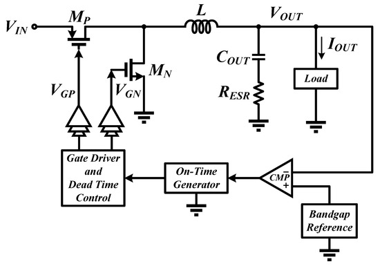
Figure 1.
Schematic of the constant on-time DC-DC buck converter.
Compared with electrolytic capacitors, a multilayer ceramic capacitor (MLCC) has the advantages of long used time, low cost, better high frequency response, and small size. However, the use of an MLCC as the output capacitor of a DC-DC buck converter in a variable operating frequency system must be accompanied by additional control mechanisms to maintain system stability. Hence, there are some studies that propose a combination of low ripple of output voltage and system stability [12,13]. In addition, since the variable frequency control system has a gradually increasing switching loss ratio of the power transistor at a light load, the constant on-time control can improve the efficiency of the DC-DC buck converter by lowering the operating frequency.
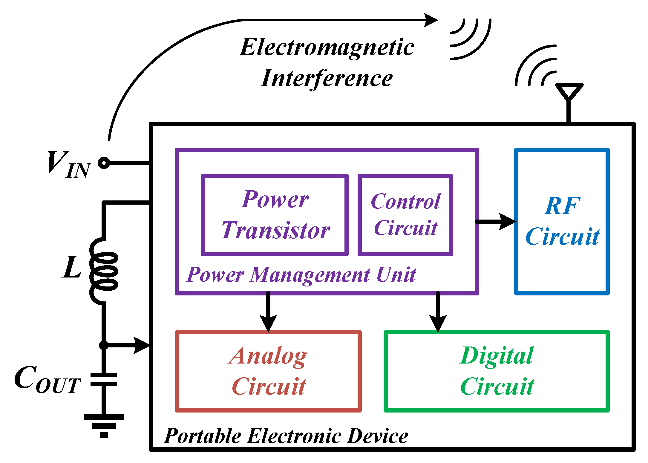
Switching regulators have many advantages, such as high conversion efficiency and small size. However, there are still some shortcomings that must be carefully considered, the most important of which is the electromagnetic interference (EMI) of the DC-DC buck converter [14,15,16]. Figure 2 shows the EMI of a portable electronic device. EMI is an electromagnetic noise that is not conducive to other systems during the normal operation of a DC-DC buck converter, which is a serious problem for safety regulations. Therefore, in order to eliminate the influence of EMI, it is necessary to modify the layout of the printed circuit board of the switching regulators or to add additional control circuits, which will increase the cost of the product. Random switching frequency is one of the most effective ways to reduce EMI [17]. This method disperses the power of spurs of the converter in the frequency domain by randomly adjusting the switching frequency. However, the disadvantage is that the instantaneous jitter of the switching frequency is too large, which will increase the ripple of the output voltage. To suppress the EMI of the DC-DC buck converter and the ripple of output voltage, the triangular spread-spectrum mechanism is presented in this paper. The EMI of the DC-DC buck converter is introduced in Section 2. The circuit implementation of the proposed triangular spread-spectrum mechanism is described in Section 3. Finally, the experimental results and conclusions are shown in Section 4 and Section 5, respectively.
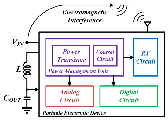
Figure 2.
Electromagnetic interference of the portable electronic device.
2. Electromagnetic Interference of the DC-DC Buck Converter
Electromagnetic compatibility (EMC) is a very important issue for switching regulators. If the standard of EMC is not taken into account in the design of the switching regulator, it will take more time to deal with the effects of EMI, such as modifying the layout of the printed circuit board of the switching regulators.
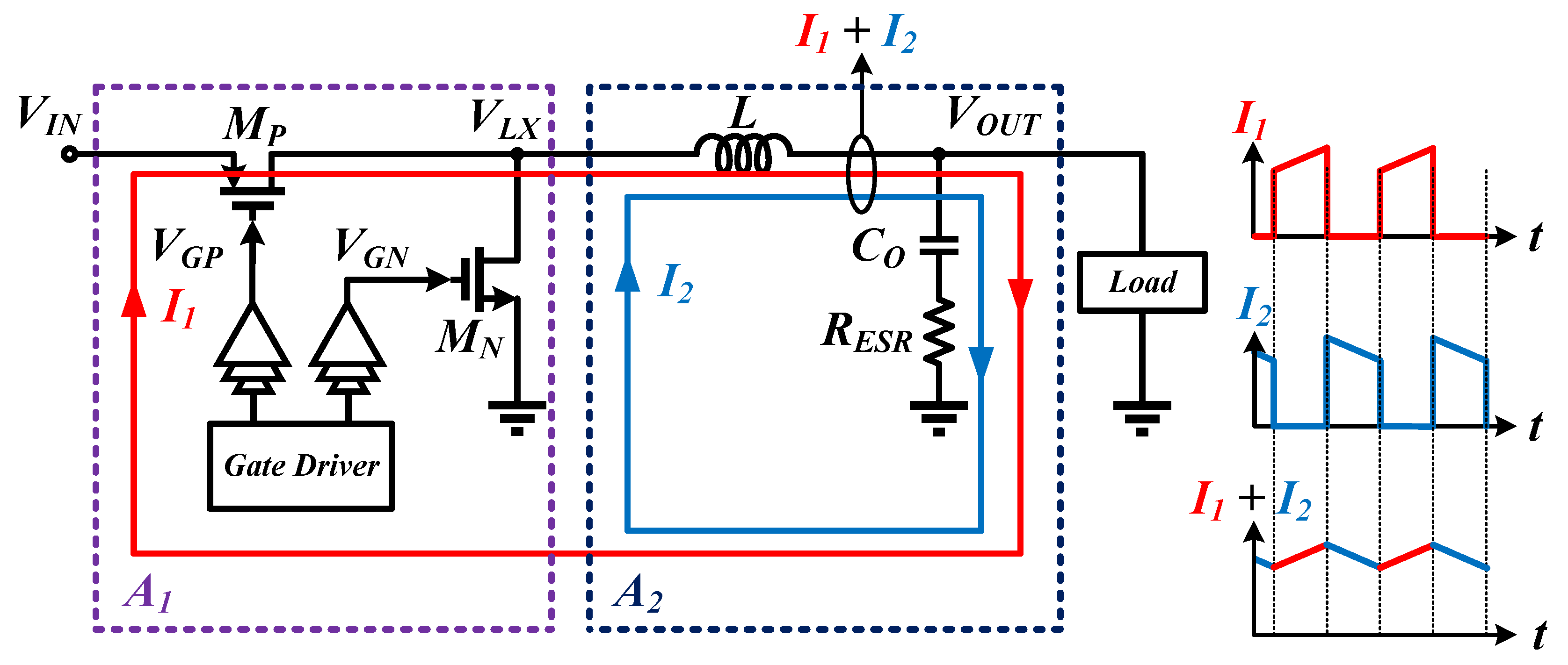
Figure 3 depicts the inductor current distribution of the DC-DC buck converter. There are two dramatically varying current loops (I1 and I2) in the DC-DC buck converter. First, when the power transistor Mp is turned on, the current loop I1 passes through the input voltage VIN, the power transistor Mp, the inductor L, the output capacitor COUT, and the load. Next, in order to maintain the continuity of the inductor current, the power transistor Mn will be turned on. The current loop I2 flows through the power transistor Mn, the inductor L, the output capacitor COUT, and the load at this time. According to the operating principle of the switching regulator, we can find that the current loops I1 and I2 are not continuous. This will therefore cause a large current change rate, resulting in the generation of high frequency components. There are two areas (A1 and A2) included in the inductor current distribution of the DC-DC buck converter. The area A1 has a large high frequency component because only the current loop I1 passes. On the other hand, since both current loops I1 and I2 pass through the area A2, the inductor current forms a smooth and continuous triangular wave. Thus, the high frequency component of the area A2 is reduced. In summary, the EMI of area A1 will be higher than the area A2. As a result, the input terminal of the DC-DC buck converter will generate a large EMI. Consequently, the EMI of the DC-DC buck convertor can be suppressed by the spread-spectrum technique, as shown in Figure 4.

Figure 3.
Inductor current distribution of the DC-DC buck converter.
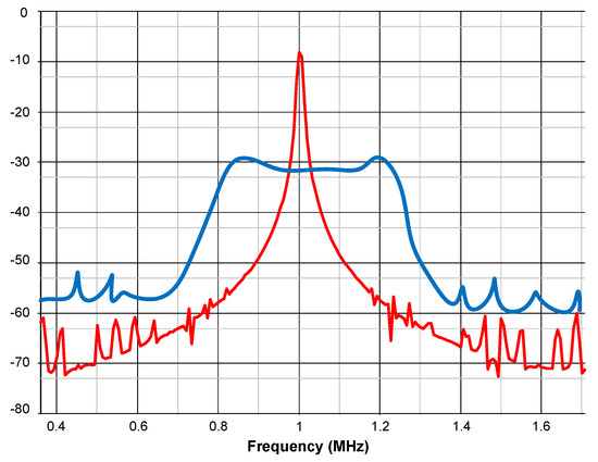
Figure 4.
Spectrum waveform with and without spread-spectrum technique.
3. Circuit Implementation
The triangular spread-spectrum mechanism proposed in this paper uses a triangular wave to modulate the on-time of the power transistor. Due to the switching frequency being gradually increased or decreased, the waveform of the inductor current is smoother. In addition, reducing the ripple of output voltage can also make the output voltage of the converter more stable. The block diagram of the proposed DC-DC buck converter is shown in Figure 5. To realize the spur reduction, this paper proposes a low EMI DC-DC buck converter with a triangular spread-spectrum mechanism that effectively mitigates the effects of EMI. In addition, the system stability and the ripple of the DC-DC buck converter are improved by the inductive DC resistance (DCR) current sensing circuit.
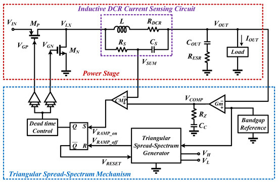
Figure 5.
Block diagram of the proposed DC-DC buck converter.
3.1. Proposed Triangular Spread-Spectrum Generator
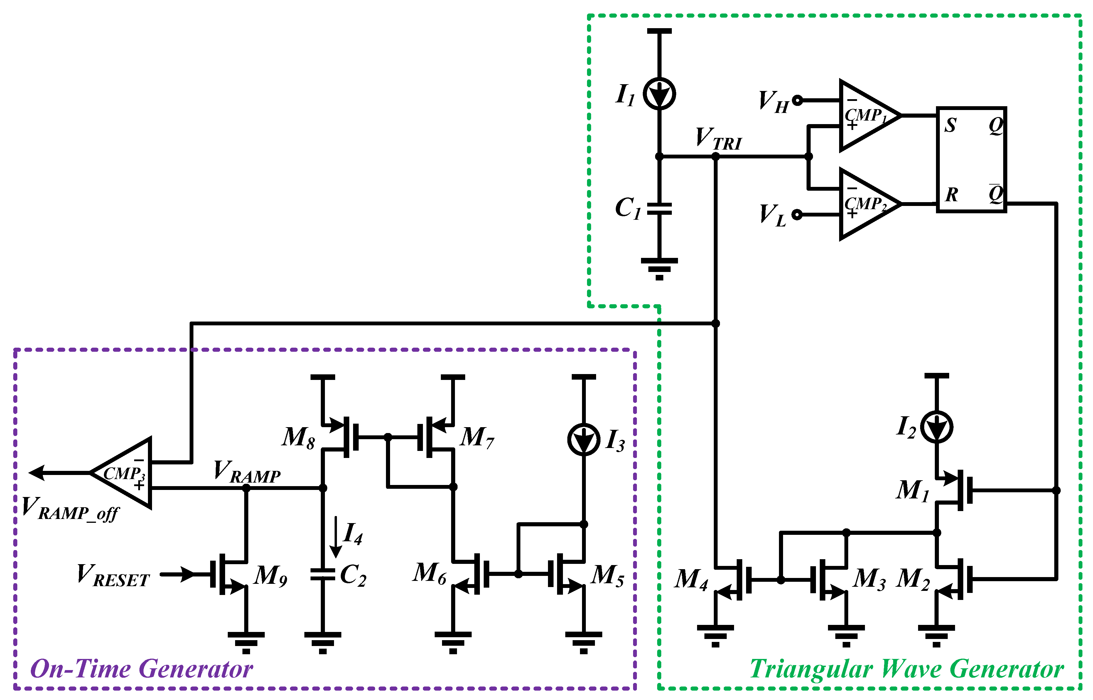
The schematic of the proposed triangular spread-spectrum generator and simulation waveform are shown in Figure 6 and Figure 7, respectively. The triangular spread-spectrum generator is composed of a triangular wave generator and an on-time generator. First, the triangular wave generator includes current sources I1 and I2, a capacitor C1, comparators CMP1 and CMP2, an SR latch, and transistors M1-M4. Assuming that the initial voltage of the capacitor C1 is 0V, the SR latch will provide a high-level voltage to turn off the transistor M1. Thus, the current source I1 will charge the capacitor C1. When the voltage of the capacitor C1 is higher than the upper threshold voltage VH, a low-level voltage will be produced by the SR latch to turn on the transistor M1. If the current source I1 is designed to be half of the current source I2, the capacitor C1 will be discharged through the transistors M3 and M4 and the current source I2. When the voltage of the capacitor C1 is lower than the lower threshold voltage VL, the current source I1 will charge the capacitor C1 again. By repeating the above operation, a triangular wave VTRI can be obtained. In general, the upper threshold voltage VH and the lower threshold voltage VL will affect the slope of the triangular wave. Thus, it would appear that a smoother triangular wave has a smaller impact on the output voltage, that is, it has a lower ripple of output voltage and a smooth output voltage. Next, the on-time generator comprises a current source I3, a comparator CMP3, a capacitor C2, and transistors M5-M9. The current source I3 charges the capacitor C2 via the transistors M5-M8. When the voltage of the capacitor C2 is higher than the triangular wave VTRI, the comparator CMP3 will generate a pulse signal to the SR latch to modulate the on-time. The voltage of the capacitor C2 will be discharged at this time by using the transistor M9.
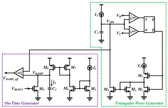
Figure 6.
Schematic of the proposed triangular spread-spectrum generator.
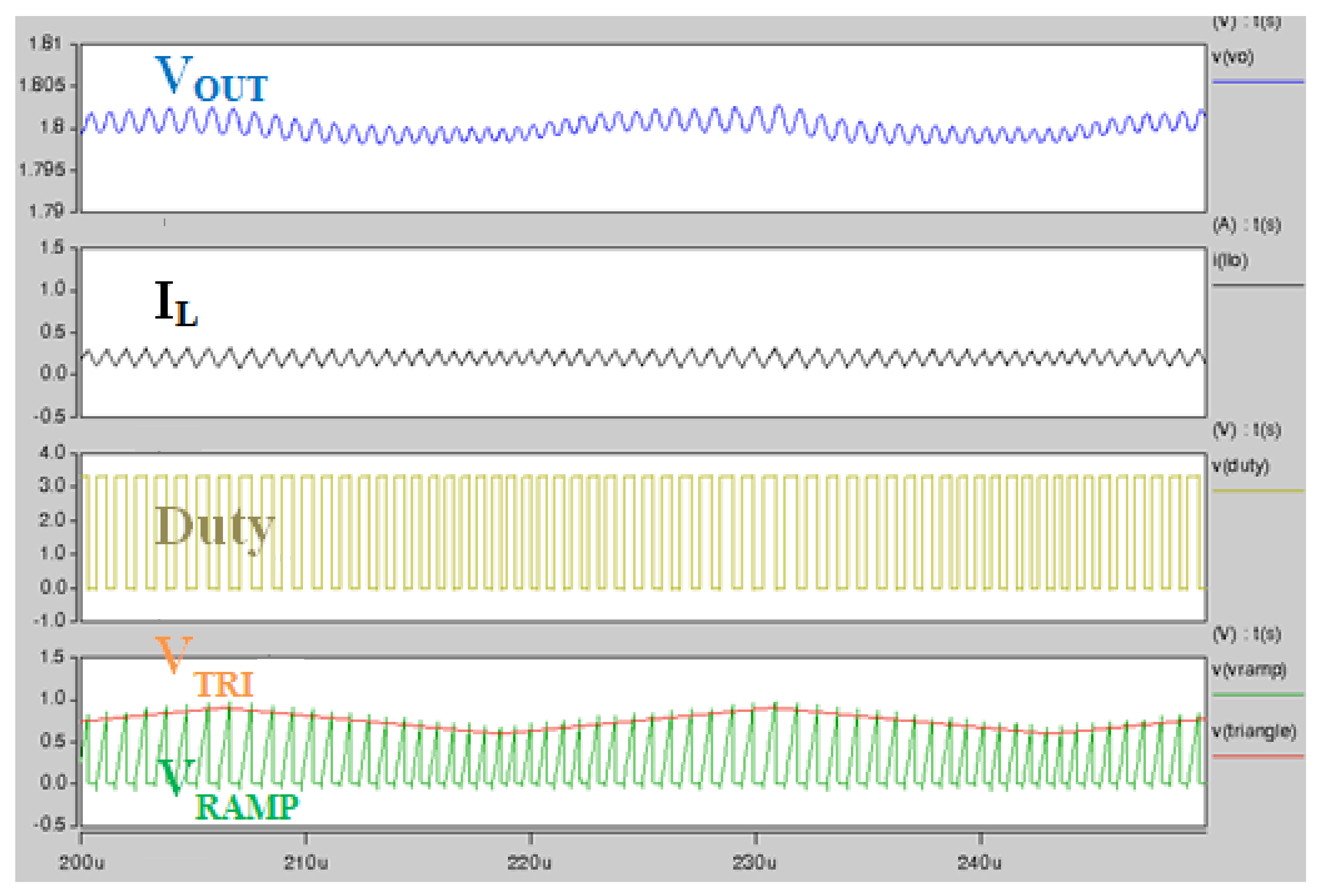
Figure 7.
Simulation waveform of the triangular spread-spectrum generator.
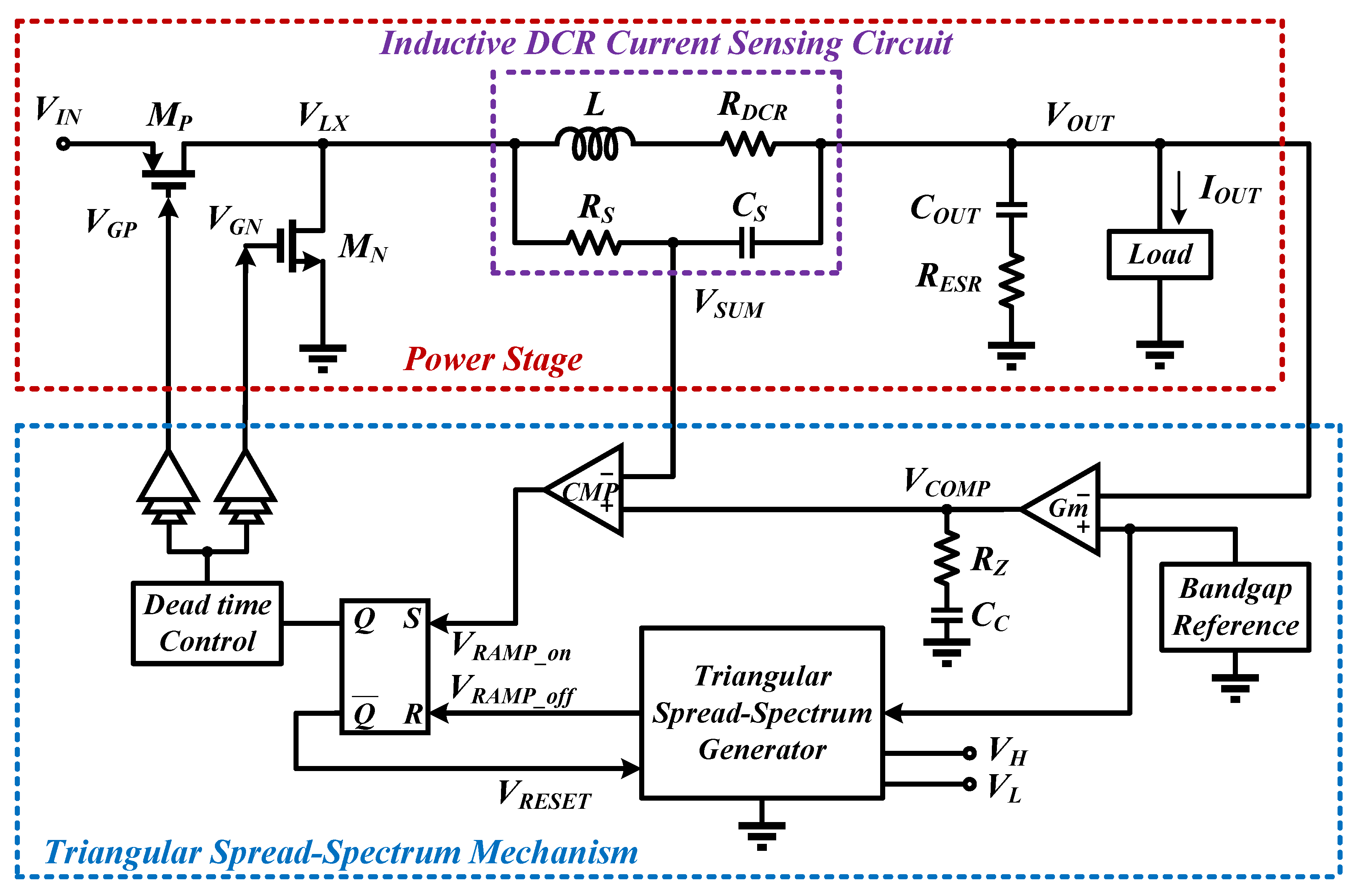
3.2. Inductive DCR Current Sensing Circuit
The inductive DCR current sensing circuit is depicted in Figure 8. Due to the reduced ripple of output voltage of the DC-DC buck converter, the output capacitor with low ESR is employed. However, lower ripple of output voltage of the DC-DC buck converter causes system instability. Thus, to prevent sensing incorrect information on the inductor current, the inductive DCR current sensing circuit is adopted to obtain information on the inductor current. It is composed of an inductor with DCR RDCR and filter circuits RS and CS. The operating principle of the inductive DCR current sensing circuit is to sense the inductor current by the inductive DCR RDCR and obtain the sensing voltage VSEN through the filter circuits RS and CS. It can be expressed as
When the time constants in Equation (1) are equal, it can be determined as
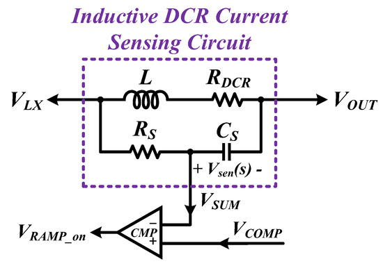
Figure 8.
Schematic of the inductive DC resistance (DCR) current sensing circuit.
By substituting Equation (2) into Equation (1), VSEN can be simplified as
The output voltage of the inductive DCR current sensing circuit VSUM can be calculated as
It can be found from Equation (4) that the output voltage of the inductive DCR current sensing circuit VSUM is composed of the output voltage of the DC-DC buck converter VOUT and the sensing voltage VSEN. Thus, even if the MLCC is used as the output capacitor COUT, the output voltage of the inductive DCR current sensing circuit VSUM can acquire the correct information on the inductor current.
4. Experimental Results
In order to verify the proposed DC-DC buck converter with the triangular spread-spectrum mechanism, the chip is implemented using TSMC 1P6M 0.18-μm CMOS technology. The chip microphotograph is shown in Figure 9, and consists of the power transistors, gate driver and proposed triangular spread-spectrum mechanism.
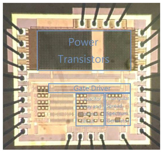
Figure 9.
Chip microphotograph.
The chip area including PADs is 1.2 × 1.15 mm2. The off-chip inductor and capacitor are adopted as 3.3 μH and 10 μF, respectively. The operating frequency ranges from 0.7 MHz to 1.3 MHz. The nominal input voltage and output voltage are 3.3 V and 1.8 V, respectively. The maximum load current is 700 mA. The experimental results are shown in Figure 10, Figure 11, Figure 12, Figure 13, Figure 14, Figure 15, Figure 16, Figure 17, Figure 18 and Figure 19, including the steady-state response, ripple of output voltage, transient recovery time, spectrum waveform and conversion efficiency.
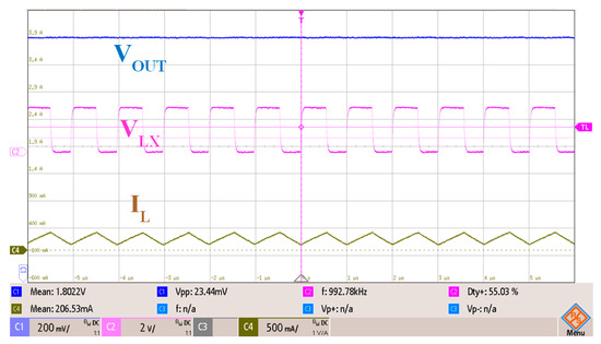
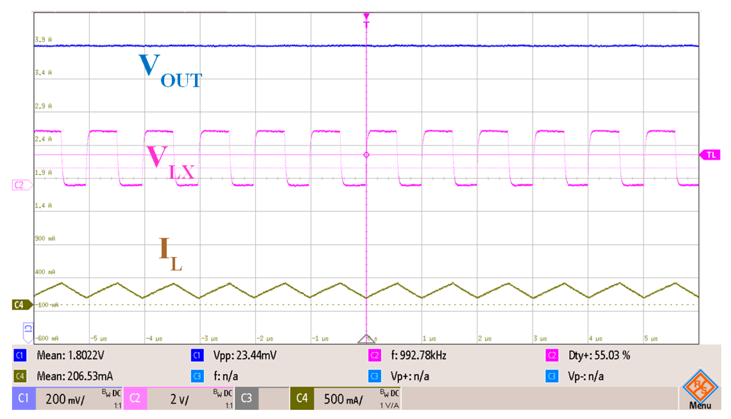
Figure 10.
Measured light load steady-state response of the proposed DC-DC buck converter (VOUT = 1.8 V; ILOAD = 200 mA).
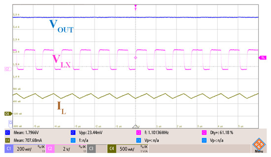
Figure 11.
Measured heavy load steady-state response of the proposed DC-DC buck converter (VOUT = 1.8 V; ILOAD = 700 mA).
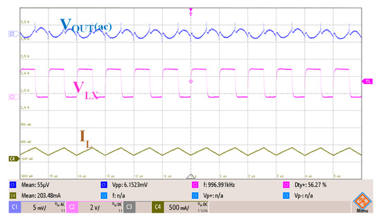
Figure 12.
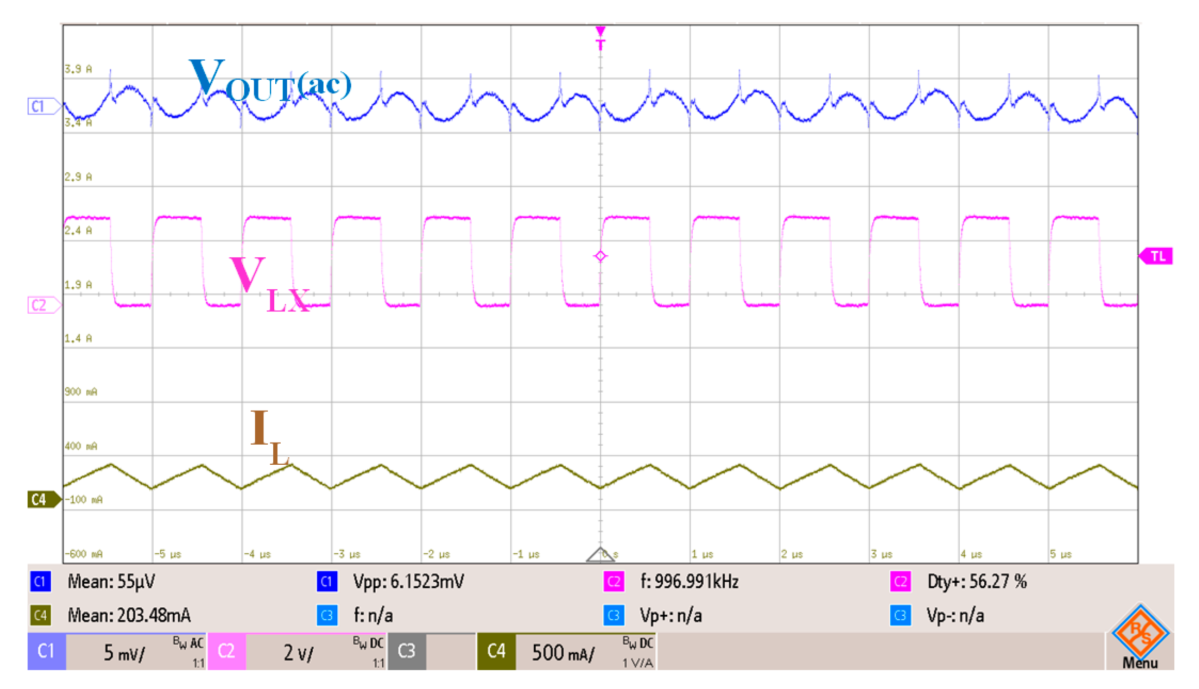
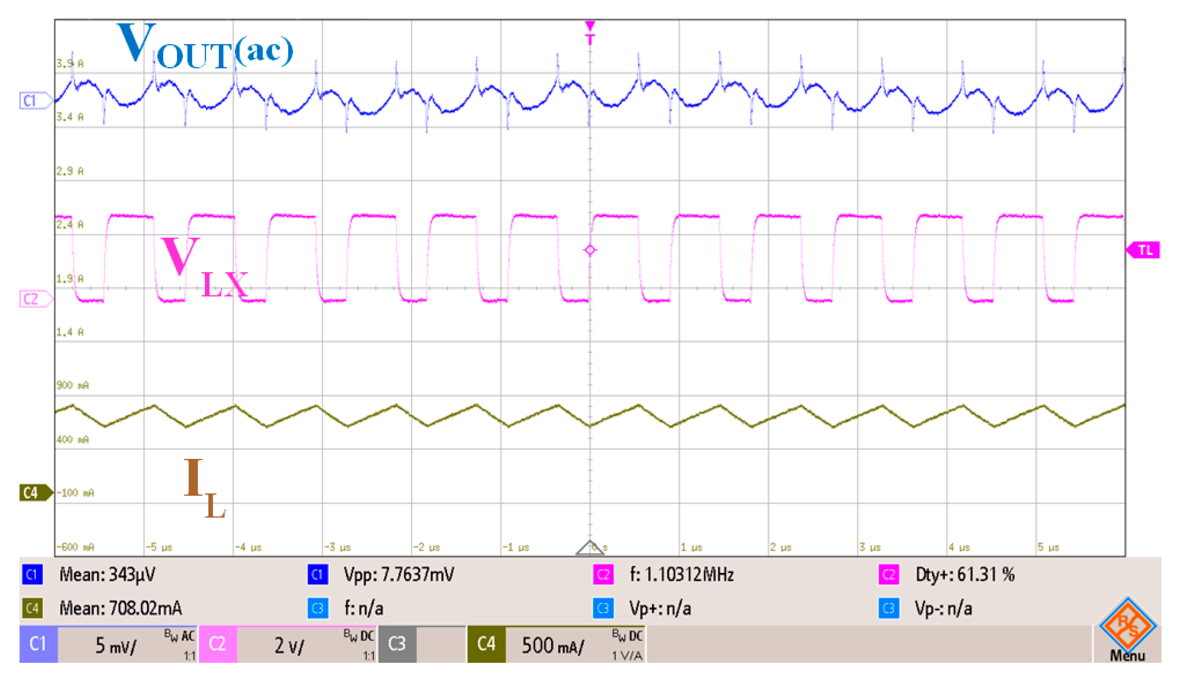
Measured light load output ripple of the proposed DC-DC buck converter (VOUT = 1.8 V; ILOAD = 200 mA).
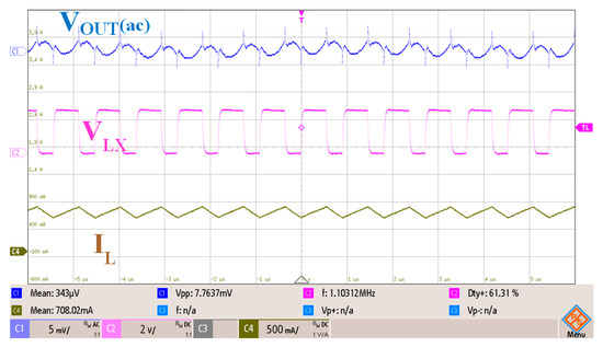
Figure 13.
Measured heavy load output ripple of the proposed DC-DC buck converter (VOUT = 1.8 V; ILOAD = 700 mA).

Figure 14.
Measured transient response of the proposed DC-DC buck converter.
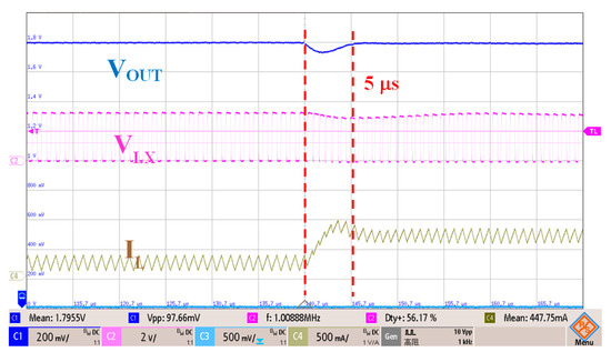
Figure 15.
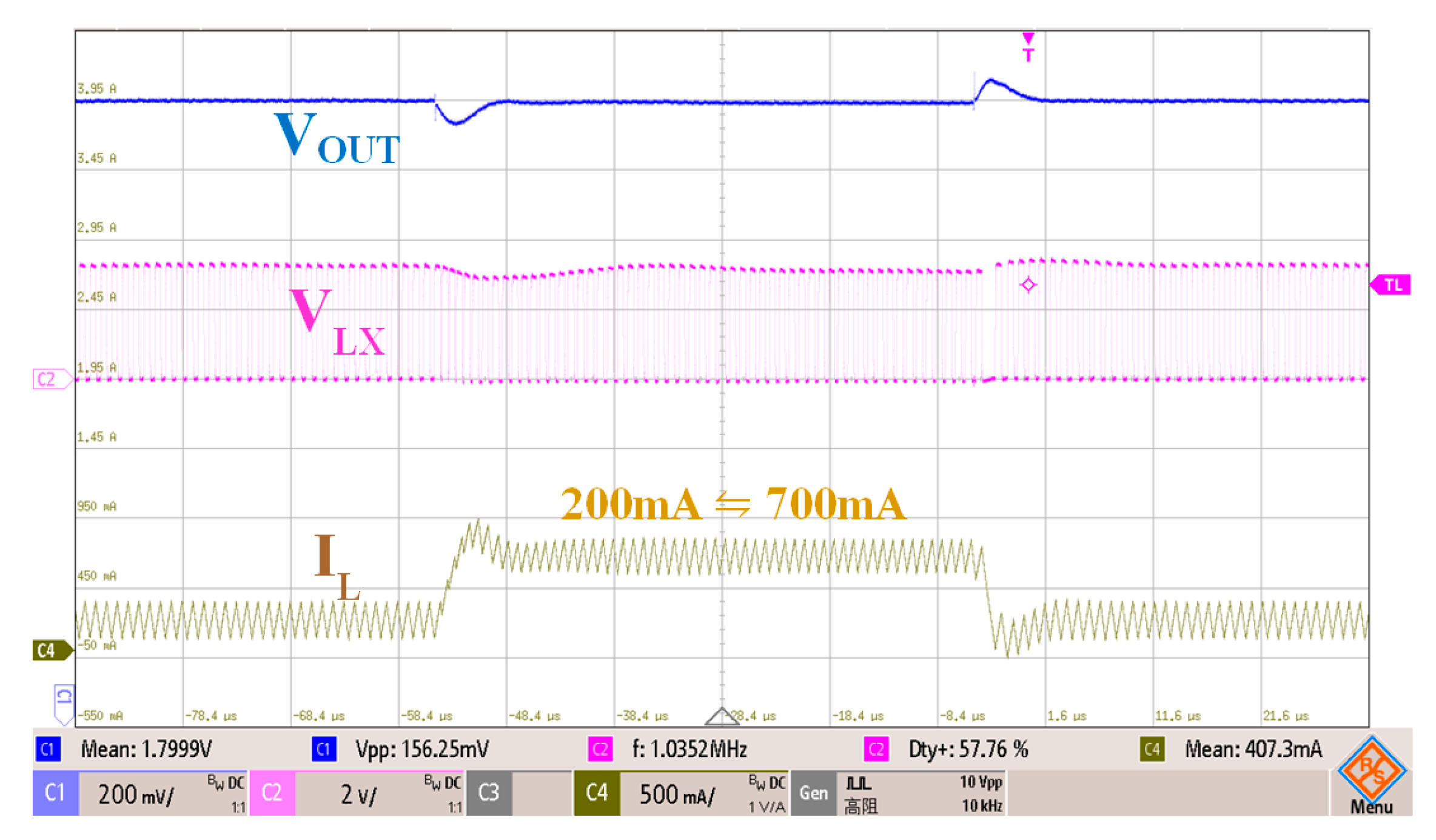
Measured transient recovery time with the proposed DC-DC buck converter for a step-up load from 200 mA to 700 mA.
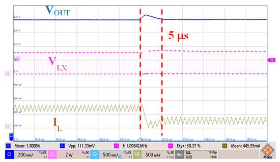
Figure 16.
Measured transient recovery time with the proposed DC-DC buck converter for a step-down load from 200 mA to 700 mA.
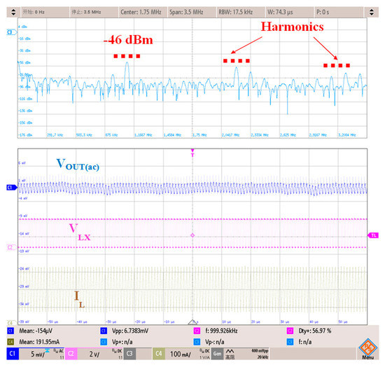
Figure 17.
Measured spectrum waveform without the proposed triangular spread-spectrum mechanism.
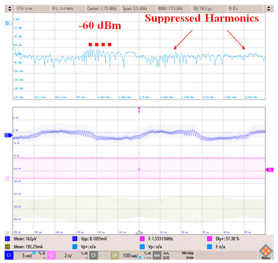
Figure 18.
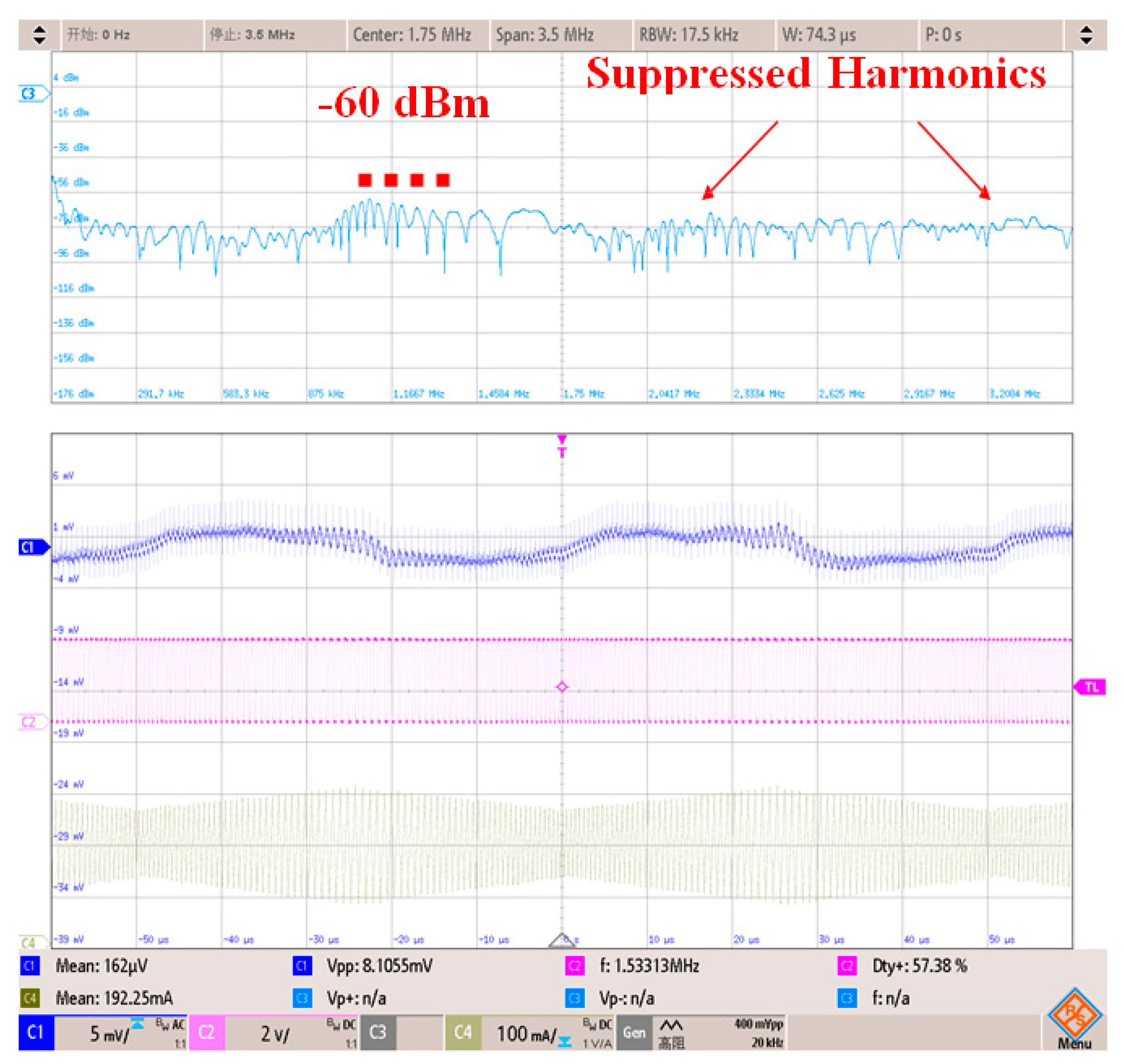
Measured spectrum waveform with the proposed triangular spread-spectrum mechanism.
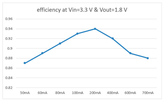
Figure 19.
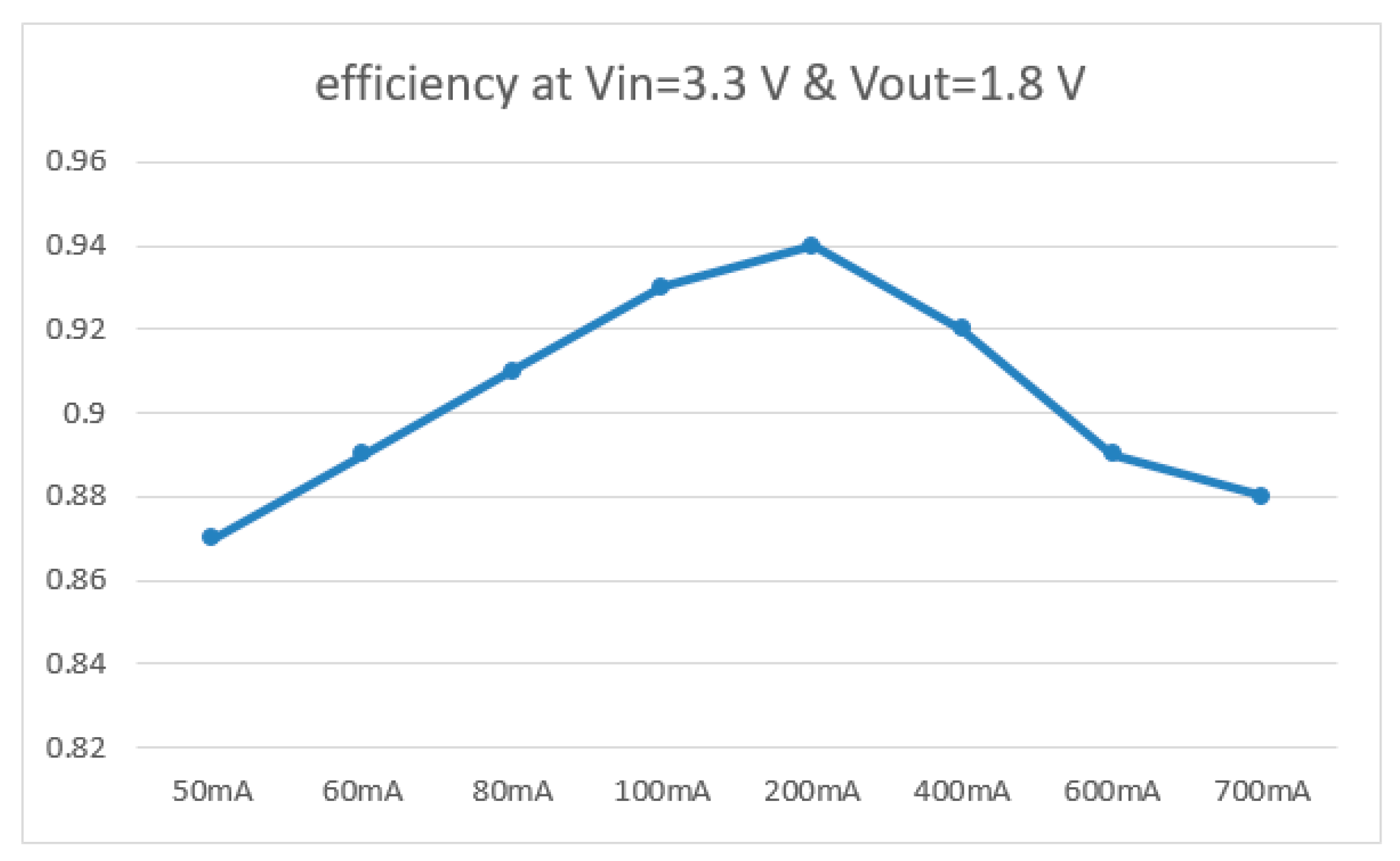
Measured conversion efficiency of the proposed DC-DC buck converter.
Figure 10 and Figure 11 show the measured results of the light load (ILOAD = 200 mA) and the heavy load (ILOAD = 700 mA) steady-state response of the proposed DC-DC buck converter, respectively. The measured results include the output voltage VOUT of the DC-DC buck converter, the connection of the power transistors VLX and the inductor current IL. It can be found that the output voltages of the proposed DC-DC buck converter are both 1.8 V from the measured results.
The light load (ILOAD = 200 mA) and heavy load (ILOAD = 700 mA) output ripples of the proposed DC-DC buck converter, as shown in Figure 12 and Figure 13, are both less than 3 mV.
The measured transient response of the proposed DC-DC buck converter is shown in Figure 14. Figure 15 and Figure 16 depict the transient recovery times for the step-up and step-down loads of the proposed DC-DC buck converter, respectively. According to the measured results, the transient recovery time of the proposed DC-DC buck converter is 5µs for both step-up (from ILOAD = 200 mA to ILOAD = 700 mA) and step-down (from ILOAD = 700 mA to ILOAD = 200 mA) loads.
The measured spectrum waveforms of the Fast Fourier Transform (FFT) without and with the proposed triangular spread-spectrum mechanism are shown in Figure 17 and Figure 18, respectively. The measured maximum spurs of the DC-DC buck converter without and with the proposed triangular spread-spectrum mechanism are –46 dBm and –60 dBm, respectively. The experimental results show that the maximum spur of the proposed DC-DC buck converter with the triangular spread-spectrum mechanism improved by 14 dBm. The measured efficiency of the proposed DC-DC buck converter is illustrated in Figure 19. The maximum conversion efficiency is 94% when the load current is 200 mA. The specification of the proposed DC-DC buck converter with the triangular spread-spectrum mechanism is listed in Table 1.

Table 1.
Specification of the proposed DC-DC buck converter.
5. Conclusions
This paper presents the possibility of a low EMI DC-DC buck converter with a triangular spread-spectrum mechanism to reduce the EMI. The proposed triangular spread-spectrum mechanism is implemented in the chip, so there is no need to modify the PCB in order to mitigate the effect of EMI. On the other hand, reducing the ripple of output voltage of the DC-DC buck converter and maintaining system stability can be realized by the inductive DCR current sensing circuit. The chip is implemented by using the TSMC 0.18-μm 1P6M CMOS process. The chip area including PADs is 1.2 × 1.15 mm2. The input voltage range is 2.7–3.3 V and output voltage is 1.8 V. The maximum load current is 700 mA. The off-chip inductor and capacitor are 3.3 μH and 10 μF, respectively. The measured results show that the maximum spur of the proposed DC-DC buck converter with a triangular spread-spectrum mechanism is suppressed to 14 dBm. Moreover, the transient recovery time of step-up and step-down loads are both 5 μs. The measured efficiency is 94% when the load current is 200 mA.
Author Contributions
J.-Y.L. and Y.-C.H. conceived and designed the architecture and experiment. Y.-D.L. performed the experiment. Y.-C.H. wrote the paper. J.-Y.L. provided all material for the experiment, and supervised the design, analysis, experiment, and editing of the paper. All authors have read and agreed to the published version of the manuscript.
Funding
This research received no external funding.
Acknowledgments
The authors would like to thank the Taiwan Semiconductor Research Institute (TSRI) for chip fabrication and technical support.
Conflicts of Interest
The authors declare no conflict of interest.
References
- Hsu, Y.-C.; Ting, C.-Y.; Hsu, L.-H.; Lin, J.-Y.; Chen, C.-P. A transient enhancement DC-DC buck converter using dual operating mode control technique. IEEE Trans. Circuits Syst. II Exp. Briefs 2018, 66, 1376–1380. [Google Scholar] [CrossRef]
- Suh, J.-D.; Seok, J.; Kong, B.-S. A fast response PWM buck converter with active ramp tracking control in load transient period. IEEE Trans. Circuits Syst. II Exp. Briefs 2018, 66, 467–471. [Google Scholar] [CrossRef]
- Lee, C.-F.; Mok, P.-K.-T. A monolithic current-mode CMOS DC-DC converter with on-chip current-sensing technique. IEEE J. Solid State Circuits 2004, 39, 3–14. [Google Scholar] [CrossRef]
- Wu, K.-I.; Hwang, B.-T.; Chen, C.-P. Synchronous double-pumping technique for integrated current-mode PWM DC–DC converters demand on fast-transient response. IEEE Trans. Power Electron. 2017, 32, 849–865. [Google Scholar] [CrossRef]
- Lee, Y.-H.; Huang, S.-C.; Wang, S.-W.; Chen, K.-H. Fast transient (FT) technique with adaptive phase margin (APM) for current mode DC–DC buck converters. IEEE Trans. Very Large Scale Integr. (VLSI) Syst. 2012, 20, 1781–1793. [Google Scholar] [CrossRef]
- Huang, H.-H.; Chen, C.-L.; Chen, K.-H. Adaptive window control (AWC) technique for hysteresis DC-DC buck converters with improved light and heavy load performance. IEEE Trans. Power Electron. 2009, 24, 1607–1617. [Google Scholar] [CrossRef]
- Wu, K.-I.; Hung, S.-H.; Shieh, S.-Y.; Hwang, B.-T.; Hung, S.-Y.; Chen, C.C.-P. Current-mode adaptively hysteretic control for buck converters with fast transient response and improved output regulation. In Proceedings of the IEEE International Symposium on Circuits and Systems (ISCAS), Melbourne, Australia, 1–5 June 2014; pp. 950–953. [Google Scholar]
- Hwang, Y.-S.; Wu, T.-H.; Lu, M.-X.; Chen, J.-J. Sub-1-V fast-response hysteresis- controlled CMOS buck converter using adaptive ramp techniques. IEEE Trans. Very Large Scale Integr. (VLSI) Syst. 2013, 21, 1608–1618. [Google Scholar]
- Lin, Y.-C.; Chen, C.-J.; Chen, D.; Wang, B. A ripple-based constant on-time control with virtual inductor current and offset cancellation for DC power converters. IEEE Trans. Power Electron. 2012, 27, 4301–4310. [Google Scholar] [CrossRef]
- Chen, W.-W.; Chen, J.-F.; Liang, T.-J.; Wei, L.-C.; Huang, J.-R.; Ting, W.-Y. A novel quick response of RBCOT with VIC ripple for buck converter. IEEE Trans. Power Electron. 2013, 28, 4299–4307. [Google Scholar] [CrossRef]
- Li, C.-H.; Chiu, H.-J.; Lo, Y.-K.; Wang, C.-C. Adaptive on-time control with adjustable virtual ripple and offset cancellation for buck converter. IET Power Electron. 2015, 12, 2418–2428. [Google Scholar] [CrossRef]
- Chen, C.; Chen, D.; Tseng, C.; Chang, Y.; Wang, K. A novel ripple-based constant on time control with virtual inductor current ripple for buck converter with ceramic output capacitors. In Proceedings of the IEEE APEC, San Francisco, CA, USA, 21–25 February 2011; pp. 1488–1493. [Google Scholar]
- Chen, W.-C.; Wang, C.-S.; Su, Y.-P.; Lee, Y.-H.; Lin, C.-C.; Chen, K.-H.; Du, M.-J. Reduction of equivalent series inductor effect in delay ripple reshaped constant on-time control for buck converter with multilayer ceramic capacitors. IEEE Trans. Power Electron. 2013, 28, 2366–2376. [Google Scholar] [CrossRef]
- Lee, Y.-H.; Wang, S.-J.; Chen, K.-H. Quadratic differential and integration technique in V2 control buck converter with small ESR capacitor. IEEE Trans. Power Electron. 2010, 25, 829–838. [Google Scholar]
- Su, Y.-P.; Lee, Y.-H.; Chen, W.-C.; Chen, K.-H.; Lin, Y.-H.; Tsai, T.-Y.; Huang, C.-C.; Lee, C.-C. A pseudo-noise coded constant-off-time (PNC-COT) control switching converter with maximum 18.7-dBm peak spur reduction and 92% efficiency in 40 nm CMOS. In Proceedings of the IEEE Symposium on VLSIC, Kyoto, Japan, 11–14 June 2013; pp. C170–C171. [Google Scholar]
- Du, Y.; Liu, Q.; Huang, A.-Q. Current-mode hysteretic buck converter with spur-free control for variable switching noise mitigation. In Proceedings of the ECCE, Raleigh, NC, USA, 15–20 September 2012; pp. 1849–1856. [Google Scholar]
- Liu, P.-J.; Tai, J.-N.; Chen, H.-S.; Chen, J.-H.; Chen, Y.-J. Spur-reduction design of frequency-hopping DC–DC converters. IEEE Trans. Power Electron. 2012, 27, 4763–4771. [Google Scholar] [CrossRef]


© 2020 by the authors. Licensee MDPI, Basel, Switzerland. This article is an open access article distributed under the terms and conditions of the Creative Commons Attribution (CC BY) license (http://creativecommons.org/licenses/by/4.0/).