Abstract
Battery-less sensors need a fast and stable wireless charging mechanism to ensure that they are being correctly activated and properly working. The major drawback of state-of-the-art wireless power transfer solutions stands in the maximum Equivalent Isotropic Radiated Power (EIRP) established from local regulations, even using directional antennas. Indeed, the maximum transferred power to the load is limited, making the charging process slow. To overcome such limitation, a novel method for implementing an effective wireless charging system is described. The proposed solution is designed to guarantee many independent charging contributions, i.e., multiple tones are used to distribute power along transmitted carriers. The proposed rectenna system is composed by a set of narrow-band rectifiers resonating at specific target frequencies, while combining at DC. Such orthogonal frequency schema, providing independent charging contributions, is not affected by the phase shift of incident signals (i.e., each carrier is independently rectified). The design of the proposed wireless-powered system is presented. The main advantage of the solution is the voltage delivered to the load, which is directly proportional to the number of used carriers. This is fundamental to ensure fast sensor wakes-up and functioning. To demonstrate the feasibility of the proposed system, the work has been complemented with the manufacturing of two rectennas, and the analysis of experimental results, which also validated the linear relationship between the number of used carriers.
1. Introduction
With the advent of Internet of Things (IoT) era, the capacity of charging devices using Radio Frequency (RF) waves gained momentum. As such, wireless device charging calls for Wireless Power Transfer (WPT) techniques. Nowadays, Wireless Sensor Networks (WSN)s are placed everywhere and use smart devices to acquire environmental data and process them locally, thus possibly demanding for a wireless power source to enhance their functioning and lifetime [1,2]. Indeed, addressing this challenge comes with the promise of reducing operator intervention on the networks for substituting and disposing old batteries; moreover, batteries have a negative environmental impact [3,4]. To this purpose, many ways exist to provide energy to autonomous sensors; by means of more conventional solar, thermal, and vibration energy harvesting techniques to name a few. Unlike the aforementioned techniques, in this work we target and analyze the opportunity to remotely powering end-devices via radio waves [5,6].
1.1. Challenges, Opportunities, and Applications
The perspective of remotely powering WSNs by means of RF waves, gained notable interest over the past years [7]. The techniques for wirelessly transferring power can be categorized into two classes, depending on the nature of the RF source. On one side, in Wireless Power Harvesting (WPH) the end-nodes extract power from existing services using RF signals. For instance, Vyas and et al. [8] describe the architecture of a battery-less sensor powered by the Digital Video Broadcast (DVB) terrestrial signals, whereas in [9], the authors exploited cellular radio technologies. On the other hand, in WPT, the power is extracted from RF waves intentionally transmitted by a dedicated emitter. Techniques belonging to this class find large application in WSNs, Near Field Communication (NFC), and Radio Frequency Identification (RFID)-based systems [10,11].In this work we address the challenge of wirelessly powering a remote device through a novel WPT technique where the power source is a multi-carrier transmitter. As such, the rectenna system is a multi-frequency-based circuit able to rectify each carrier independently. Each frequency slot contributes exclusively at Direct Current (DC) for the charging of a supercapacitor, which actually backs the remote sensor.
1.2. State-of-the-Art
Prior works focused on maximizing the efficiency of the single rectifier [12]. In [13,14], the impact of the antenna input impedance on charging performance has been addressed. It is shown that such impedance affects the charging time, although there is no variation in the overall voltage delivered to the load. To overcome this limitation, output voltage boosters are usually considered. They consist of multi-stage diode-based rectifiers, as for example the Dickson charge pump [15,16,17,18]. However, because of the increase in the losses, it has been shown that a maximum of three stages is possible; this finding is reported by the work in [17]. A way to enhance the rectifier efficiency is to perfectly match the input impedance of the antenna with the one of the diode [16]. However, diodes are nonlinear circuits and the internal impedance changes according to the input power level. As realized in [19], each input power level needs a different matching circuit to maximize the efficiency of the power conversion. Although the rectenna may potentially achieve the maximum efficiency, its capability to deliver power may not be enough to supply a real load [14]. Indeed, regulations on frequency spectrum strongly limit the Equivalent Isotropic Radiated Power (EIRP) [7], even in the case of using reconfigurable directive antennas to focus the overall radiation towards the target sensor [20]. For this reason, several solutions employ high-gain antennas as, for instance, pre-aligned phased arrays, albeit limited to a static scenario [21,22]. Dynamic scenarios imply the nodes may change their spatial position over the time, thus demanding for the reconfiguration of the main antenna beam, which comes with a high energy cost that is unjustified for such kind of energy storage systems [2]. Tests with rectenna arrays (using single carrier) are reported in [16]. The authors compare two configurations: (i) a rectenna array with RF combining (i.e., single diode-rectifier), and () rectenna array with DC combining (i.e., each radiating element has a diode-rectifier). The latter has proven to perform better as it is less sensitive to phases of the incident RF signal. Finally, an alternative solution is based on a multi-band antenna coupled with a single rectifier, as in [3,5,23,24,25,26,27]. In these works, signals operating at different frequencies are added together at RF and the resulting envelop signal does not guarantee a reliable rectification in environment rich of reflections. In this paper, we address this main drawback.
1.3. Related Work
In this work, a WPT system formed by multiple narrow-band rectifiers is presented. The proposed architecture is implemented as a stack of frequency spaced rectennas. In turn, each rectenna can also be composed of an array antenna to increase the receive gain of each frequency. Basically, each rectenna is designed to rectify a signal oscillating at a specific frequency, and each rectifier provides independent DC contribution. These contributions are combined at DC, while the phase and the frequency of incident RF signals can be neglected. The advantage of the proposed WPT system is twofold. First, it overcomes the EIRP limitation [14,20,21,22], as if on a RF channel the transmitted power shall be under a specified power level (defined by regulations), it is still possible to transmit the same power level on another RF channel, while the contribution at DC is doubled at the receiver side. This scheme can be extended over an arbitrary number of frequency channels. Second, multi-band and/or wide-band antennas with a single feed receive an envelope signal whose shape strictly depends on the way incident RF signals combine with each other in terms of phase and frequency [3,5,23,24,25,26,27]. However, the best configuration of phases and frequencies that maximize the power transferred to the load is unpredictable in real scenarios. Moreover, propagation channels change very fast over the time. Therefore, such solutions are not able to ensure sensors wake-up and operation in all possible scenarios. Instead, the proposed work demonstrates the ability to deliver the required voltage to the load, where the output voltage is controlled by the number of carriers employed, irrespective of their phase and frequency. The main drawback of the proposed WPT system is related to the number of rectennas used, i.e., one for each carrier employed.Therefore, the system dimensions can grow fast, especially at low frequencies. Of course, by increasing the operation frequency, the size of the rectifiers reduce accordingly, but also the operative distance, as the attenuation of RF signals is proportional to the distance to cover and to their frequency.
2. Architecture Overview and Design
A rectenna consists of an antenna connected to a rectifier circuit aiming to provide DC power from the received RF signal. The proposed scheme consists of a multitude of rectennas, each operating at a different frequency. The antenna is the fundamental element to select the desired RF signal from the environment. As the carrier spacing among transmitted tones is established, then the bandwidth of each antenna needs to be accurately designed to minimize inter-elements coupling. In that way, the Continuous Wave (CW) impinging on one antenna is minimally perceived by the others. The design of the proposed system and its equivalent model is deeply discussed in the following.
2.1. Antenna Design
This section describes the design procedure of the probe-feed squared-patch antenna that will be used in this work (see Figure 1a). The transmission line model is depicted in Figure 1b from which the equivalent circuit parameters are then retrieved [28,29,30]. Microstrip patch antennas have been chosen for two reasons: first, they are simple to build, and second, the squared shape provides a high frequency selectivity. The design formulae can be found in [31]. Algorithm 1 shows the procedure exploited to design the squared patch antenna. Given the target resonance frequency and the antenna substrate (dielectric , thickness h expressed in millimeters), a squared patch is obtained by iterating on the patch dimensions (i.e., W and L). In Algorithm 1, the guided wavelength is described as
where c is the speed of light and is the effective dielectric constant described in Equation (2).
| Algorithm 1: Design procedure of a squared patch antenna |
 |
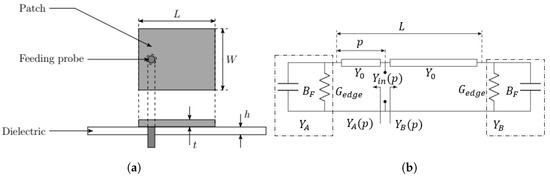
Figure 1.
Illustrative schematic of a probe-feed squared-patch antenna (a) and its corresponding transmission line model (b).
The extension length due to fringing effects is estimated by Equation (3).
The transmission line model for the patch antenna (shown in Figure 1b) consists of two radiating slots separated by a distance L. These loads are described by Equation (4):
As such, the two loads represent a parallel admittance composed by a conductance and susceptance , which in turn are estimated via Equations (5) and (6).
The resistive part of the antenna input impedance is a function of the probe position p along the patch length L and can be estimated by plotting Equation (7):
The input impedance is obtained by moving the edge loads to the selected probe position p, as described in Equations (8) and (9). For the sake of simplicity, admittance is used instead of impedance.
where is the reference admittance. Finally, to build the equivalent resonator circuit, the antenna quality factor is used. This parameter is described by Equation (10):
where is the antenna bandwidth. judges on the frequency selectivity and has to be accurately chosen based on the carrier spacing (i.e., to minimize coupling effects among the antennas).
2.2. Equivalent RLC Resonator Circuit
The patch antenna is a resonant structure whose circuital model can be implemented by a RLC resonator, as illustrated in [29]. The circuit is described by Equation (11):
where , , and are the resistance, inductance, and capacitance of the circuit, respectively, and the quality factor is shown in Equation (12).
The transition from the physical model to the circuit model is obtained by matching the quality factor of the antenna with the one of a resonator circuit, as in Equation (13), which leads to the same frequency behavior.
From Equation (13), the equivalent capacitance and inductance are obtained (Equations (14) and (15), respectively):
where is the resistance at resonance and needs to match the radiation resistance of the antenna, as in Equation (16).
The additional series inductance generated by the probe feed has not been considered in this model since the diode is directly soldered at the feeding point p. For an estimation of such a parasitic component the reader can refer to the work reported in [32,33].
2.3. Rectifier Efficiency Calculation
In this work, a single stage half-wave rectifier has been exploited. The circuit consists of a diode directly connected to the antenna feeding point. In addition, a small capacitor is used to stabilize the rectified waveform. Generally, to give a performance parameter of a rectifier, the power efficiency is used. This parameter describes the quantity of power that is actually delivered to a specific load, according to Equation (17):
where is the overall time-averaged power entering into the circuit, as described in Equation (18):
where is the power level emitted by the i-th equivalent carrier generator. The output power () is described as
where represents the voltage applied to the target load .
2.4. Analytical Model of the Proposed WPT System
As the proposed system relies on multiple rectennas providing independent voltage contributions, then the voltage delivered to the load () is described by the Equation (20):
where represents the rectified voltage by the rectenna and is the number of used channels. Therefore, we expect that the overall voltage delivered to the load is a linear combination of voltage generators connected in series to the target load . When the received signal is composed by tones of equal magnitude, then each rectenna provides the same voltage contribution and the voltage across the load becomes as in Equation (21):
Finally, we expect the output power delivered to the load provides (Equation (22)):
3. Simulation
3.1. Simulation Model
Figure 2 depicts the equivalent circuit describing the behavior of the proposed WPT system. It is made up by four-channel rectennas with a 50 MHz frequency spacing (i.e., they are designed to operate at 950 MHz, 1000 MHz, 1050 MHz, and 1100 MHz, respectively). We address an arbitrary load (for instance, for the sake of simulations we considered ). To match this circuit, i.e., to enable delivering the maximum power to the load, we designed such antennas (i.e., actually the generators) with an input impedance of 218 . The physical dimensions associated to the squared patch antenna are obtained by the iteration of Algorithm 1, and by using Equation (16), we can calculate the feed position ( mm to obtain the requested impedance). The equivalent RLC resonator circuit is obtained calculating the antenna quality factor , by exploiting Equation (10), and substituting the latter in Equations (14) and (15), which gives the value of the equivalent capacitor and the inductance. An ideal transformer is employed to decouple the RF ground from the DC ground. Such isolation ensures that the power incoming from the primary inductance is perfectly transferred to the secondary inductance, without affecting the impedance of the squared patch antenna [34]. The probe-feed of each antenna is directly connected to its own half-wave diode-based rectifier. The latter is composed by a HSMS-286C Schottky diode connected to a small capacitor ( nF), which stores the DC contribution. All channels’ contributions are combined at DC to deliver an overall power to the load . With the purpose of comparing performance, Figure 3 illustrates the simulated wideband WPT system, which is the counter part of this work. In such case, the circuit does not filter any carriers, while it rectifies the resulting signal envelop (i.e., carriers are combined at RF). This circuit is obtained by means of tuning the RLC components, while the impedance matching condition is obtained by forcing the antenna input impedance to equal the load. The frequency response of both circuits are depicted in Figure 4; curve illustrates the overall response of the proposed WPT system (dotted-line), while curve shows the behavior of the wideband rectenna. The latter has a frequency response almost constant in the frequency band of interest. Both circuits have the same attenuation in the overall bandwidth. Indeed, diode losses are related to the voltage drop. Moreover, the losses increase with the number of diodes exploited (e.g., Dickson charge pump). Despite has diodes with respect to , has been configured to perform with the same losses as the diodes work in parallel. This is reasonable, since uses a single diode to rectify the overall envelop (i.e., composed by carriers), which means each frequency slot is subjected to this diode attenuation. Conversely, exploits diodes in such a way each carrier is subjected to the attenuation of only one diode. Then, the signal entering in both circuits translate into the same losses for both configurations. For the WPT system , the greater the space among resonance points is, the lesser the contribution of adjacent carriers is. With resonance points spaced apart of 50 MHz, the attenuation between adjacent antennas is more than dB. This value is enough to demonstrate the feasibility and effectiveness of the proposed approach. The RF signal impinging on the rectifier circuits is composed by -CW generators () spaced by 50 MHz, while they are impinging on the antennas with arbitrary phases to simulate a real environmental scenario.
Figure 2.
SPICE model of the proposed rectifier ; four channels are shown, whose operative frequencies are 950 MHz, 1000 MHz, 1050 MHz, and 1100 MHz, from top to bottom, respectively (values of components are also depicted).
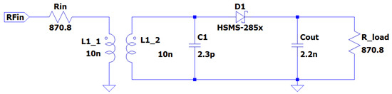
Figure 3.
SPICE model of the wide-band rectifier ; values of components are also depicted.
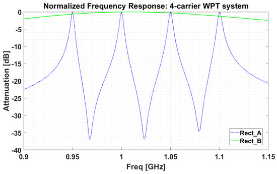
Figure 4.
Frequency response of the proposed WPT rectifier () and of the wide-band rectifier ().
3.2. Comparison with Respect to the State-of-the-Art: Simulation Results
Simulations were performed using LTSpice, a free circuit simulator tool, configured to operate in transient domain mode. To compare our proposed rectifier system () with respect to the state-of-the art (), we simulated these circuits at parity of target load , input power , and active carriers. In this simulation, means that two rectennas with radiation resistance of 218 were used thus addressing a load of , uses four rectennas and a load (this case corresponds to circuits in Figure 2 and Figure 3), and corresponds to a eight-rectenna circuit with k. Figure 5 illustrates the output voltage delivered to the load as a function of the power level emitted by the equivalent generator (), equally assigned to each carrier. In other words, corresponds to the power of a single carrier; when carriers are used, each one brings the same power level. We verified that both circuits have the same input power level during simulations. Looking at Figure 5, the wideband rectifier () curves suggest that no relevant dependence on the number of employed carriers exists. Such a system saturates at ~ V even increasing the carriers’ power level. On the other hand, curves show a direct relationship with the number of received carriers. By using two rectennas (), both systems provide almost the same performance for input power levels within 10 dBm. As this power further increases, the output voltage of saturates to 3 V, which is double the voltage applied to the load by . The same consideration stays valid for the other cases (i.e., and 8): compared to is able to boost the output voltage by 4 times (i.e., the voltage applied to the load is around 6 V) and 8 times (i.e., the voltage applied to the load is around 12 V), respectively. Such a result is very interesting from the rectifier design perspective. Indeed, given a target load , the WPT system can be designed by finding the required power level and the number of carriers (as parameters) that allow to achieve a certain output voltage, which is crucial for sensor-based applications and specifically to wake-up the sensors. Figure 6 depicts the efficiency ratio , computed by using Equation (17). The proposed system shows a significant improvement in efficiency when the power level reaches dBm. In that case, we found an efficiency ratio around 2 and 5 for and , respectively, whereas for the advantage is less prominent. The simulation demonstrates that there exists an input power level threshold beyond which the is more efficient than . The main reason for this threshold can be searched in the diodes’ voltage drop. Therefore, becomes convenient as soon as the diode-losses become negligible. Conversely, works better for power levels lower than dBm. Such analysis shows that the activation voltage of diodes judges on the required input power level to achieve a certain efficiency, while suggesting the research of very low-voltage threshold components, as for instance zero-threshold Metal-Oxide-Semiconductor Field-Effect Transistor (MOSFET) devices.
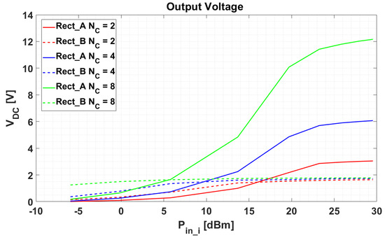
Figure 5.
Output voltage delivered to the load as a function of the input power level of the carrier generator and the number of carriers ; simulation of both and systems are shown.
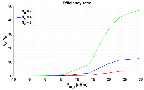
Figure 6.
Efficiency ratio: comparison of and as a function of the input power level of the carrier generator and the number of carriers .
3.3. Characterization of the Proposed Model
To demonstrate the validity of Equation (20), we characterized the proposed rectenna system (see Figure 2) by performing several simulations: first of all, the power level of equivalent generators () has been set equal for each employed carriers. Then, the overall power absorbed by the circuit (), the power delivered to the load (), the voltage across the load (), and the circuit efficiency () have been evaluated by activating the different carriers, from one at a time to four simultaneously. The simulation results are depicted in Figure 7, which shows that the output voltage increases by a factor equal to the number of active carriers, while the power increases with the square of the voltage, as expected by Equation (19). We also note that the maximum conversion efficiency is achieved when all carriers have a power level equal to . Further increasing this power level raises the output voltage; unfortunately, with a lower conversion efficiency.
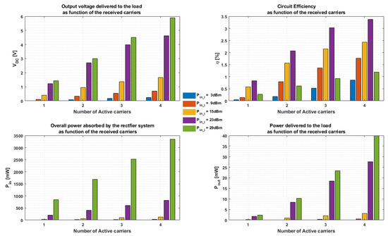
Figure 7.
Characterization of the proposed WPT system.
4. Validation and Measurements
In-field testing aims to validate the proposed system for at least the two-carrier case. To this purpose, two frequency-spaced rectennas have been implemented. They are shown in Figure 8. In order to generate the CWs, two Software Defined Radio (SDR) transceivers (i.e., the USRP B205 model) equipped with omnidirectional antennas have been used; although, the CWs can also be generated by a single transceiver. However, the use of two non-synchronous transceivers is useful to test against randomness of signals incident on the rectennas. Indeed, in such way, signals are generated from different local oscillators and emitted by two separated antennas. The tests have been performed in laboratory setting a link distance to 1 m.
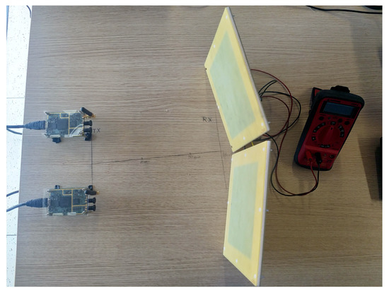
Figure 8.
Illustration of the testbed; two Software Defined Radio (SDR) transceivers are used as CW transmitters (left side), and two rectennas (right side) that implement the WPT rectifier.
4.1. Rectennas Design and Characterization
Manufactured microstrip antennas were printed on ITERA substrate (, m) targeting the frequencies 950 MHz and 1000 MHz. The overall area occupied by each rectenna is around mm (i.e., dielectric area), with the patch antennas of size mm for the lower frequency, and mm for the higher one. The rectifier is composed of the HSMS-286C Schottky diode and a capacitor of nF, as used in the simulation model. Each rectenna has been tested independently from the other to evaluate its effective frequency response. In other words, we analysed which frequency provides the maximum output voltage . In that case, a SDR transceiver has been configured to perform a frequency sweep. The measurement result is reported in Figure 9. We found a no-load voltage of V at 950 MHz for the lower-frequency rectenna, while a V peak has been found at 991 MHz for the second prototype.
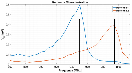
Figure 9.
Frequency characterization of the implemented rectennas; this figure illustrates the maximum no-load voltage . The black arrows allude to the transmitted carriers.
4.2. Experimental Results
We set up the SDR transceivers accordingly to the antenna responses, i.e., one to transmit at 950 MHz CW and the other at 991 MHz with equal power. The rectennas were DC combined, as illustrated in Figure 10. Here, a large capacitor F has been connected in series to the rectennas to store the overall energy from RF. The conducted test employed a multimeter to measure the voltage across the load capacitor . The charging time has been measured for a period of 25 min and logged each 30 s, i.e., 50 samples at all were collected. The measurement results are depicted in Figure 11. From these, it can be assessed that the contribution of the 950 MHz-CW provides a voltage of 0.31 V. By transmitting only the 991 MHz-CW, then the output voltage is V. The latter value is lower as expected because the higher-frequency rectenna has a lower . By transmitting both the two CWs, the output voltage raises to the final value of V. The purple dotted curve in Figure 11 shows the sum of the single contributions measured separately (i.e., it is the sum of the blue and orange curves). By comparing this curve with the measurement performed on two active carriers, it can be observed a slight difference with respect to the linear relationship. This effect is due to the non ideal rectennas that have been exploited. As the measured voltage is different from zero outside the working carrier frequency for each rectenna, there will be an additional contribution (i.e., an higher voltage value) given from each rectenna on the other carrier frequency.
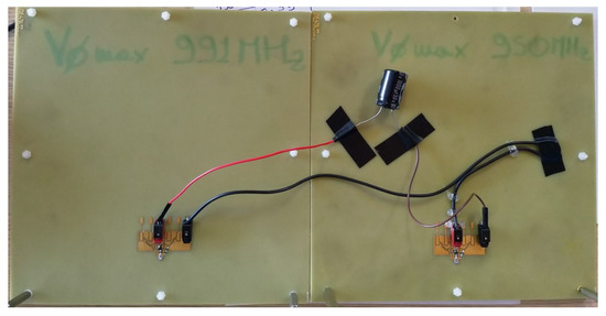
Figure 10.
Back side circuitry of the WPT system: a series of two rectennas are connected to a capacitive load of 1000 F to store the converted energy from RF.
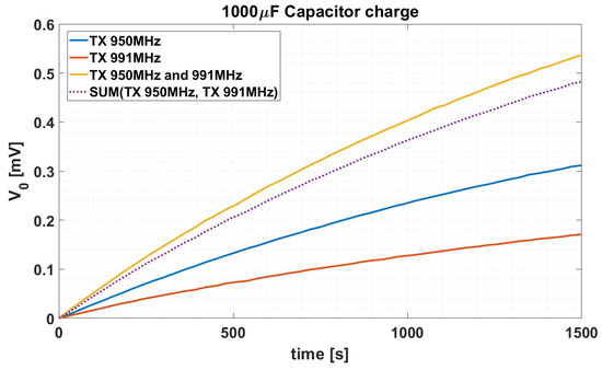
Figure 11.
Measurements of the charging time for all combinations of the transmitted CWs.
5. Conclusions and Future Perspectives
The paper presents a novel method to design a WPT system ensuring the capability of remotely activating sensors not equipped with a constant power supply source. Our research has demonstrated that the proposed system is capable to increase the voltage applied to the load. Moreover, the increase is directly proportional to the number of employed carriers. Furthermore, it has proven that the proposed WPT system is less sensitive to the difference of incident RF signal phases, thus making such system suitable for any environmental scenario. Work is currently underway to overcome the limitations of diodes. Emerging technologies, such as zero threshold MOSFET, are very promising to increasing the efficiency for lower level of the input power. A valuable extension of this work will be the introduction of the antenna gains, as the higher is the antenna gain the lower is the required incident power, thus producing more efficiency at lower levels of incident power.
Author Contributions
All the authors contributed to the several aspects presented in this work as follows: Conceptualization, S.C.; Methodology, S.C. and G.F.; Validation, A.S., G.F., G.G. and G.V.; Formal Analysis, S.C.; Investigation, S.C.; Resources, G.F.; Data Curation, S.C.; Writing-Original Draft Preparation, S.C. and A.S.; Writing-Review Editing, A.S., G.G., O.T. and G.V.; Visualization, A.S.; Supervision, O.T. and G.V.; Publication fees paid by O.T.; All authors have read and agreed to the published version of the manuscript.
Funding
This research received no external funding.
Conflicts of Interest
The authors declare no conflicts of interest.
References
- Akan, O.B.; Cetinkaya, O.; Koca, C.; Ozger, M. Internet of Hybrid Energy Harvesting Things. IEEE Internet Things J. 2018, 5, 736–746. [Google Scholar] [CrossRef]
- Ciccia, S.; Giordanengo, G.; Vecchi, G. Energy Efficiency in IoT Networks: Integration of Reconfigurable Antennas in Ultra Low-Power Radio Platforms Based on System-on-Chip. IEEE Internet Things J. 2019, 6, 6800–6810. [Google Scholar] [CrossRef]
- Congedo, F.; Monti, G.; Tarricone, L.; Bella, V. A 2.45-GHz Vivaldi Rectenna for the Remote Activation of an End Device Radio Node. IEEE Sens. J. 2013, 13, 3454–3461. [Google Scholar] [CrossRef]
- Mishra, D.; De, S.; Jana, S.; Basagni, S.; Chowdhury, K.; Heinzelman, W. Smart RF energy harvesting communications: Challenges and opportunities. IEEE Commun. Mag. 2004, 53, 70–78. [Google Scholar] [CrossRef]
- Kim, S.; Vyas, R.; Bito, J.; Niotaki, K.; Collado, A.; Georgiadis, A.; Tentzeris, M.M. Ambient RF Energy-Harvesting Technologies for Self-Sustainable Standalone Wireless Sensor Platforms. Proc. IEEE 2014, 102, 1649–1666. [Google Scholar] [CrossRef]
- Cetinkaya, O.; Akan, O.B. Electric-Field Energy Harvesting in Wireless Networks. IEEE Wirel. Commun. 2017, 24, 34–41. [Google Scholar] [CrossRef]
- Visser, H.J.; Vullers, R.J.M. RF Energy Harvesting and Transport for Wireless Sensor Network Applications: Principles and Requirements. Proc. IEEE 2013, 101, 1410–1423. [Google Scholar] [CrossRef]
- Vyas, R.J.; Cook, B.B.; Kawahara, Y.; Tentzeris, M.M. E-WEHP: A Batteryless Embedded Sensor-Platform Wirelessly Powered From Ambient Digital-TV Signals. IEEE Trans. Microw. Theory Tech. 2013, 61, 2491–2505. [Google Scholar] [CrossRef]
- Kang, S.; Lee, H.; Jang, S.; Kim, H.; Lee, I. Dynamic Time Switching for MIMO Wireless Information and Power Transfer. IEEE Trans. Commun. 2019, 67, 3978–3990. [Google Scholar] [CrossRef]
- Vita, G.D.; Iannaccone, G. Design criteria for the RF section of UHF and microwave passive RFID transponders. IEEE Trans. Microw. Theory Tech. 2005, 53, 2978–2990. [Google Scholar] [CrossRef]
- Lee, J.W.; Phan, N.D.; Vo, D.H.T.; Duong, V.H. A Fully Integrated EPC Gen-2 UHF-Band Passive Tag IC Using an Efficient Power Management Technique. IEEE Trans. Ind. Electron. 2014, 61, 2922–2932. [Google Scholar] [CrossRef]
- Valenta, C.R.; Durgin, G.D. Harvesting Wireless Power: Survey of Energy-Harvester Conversion Efficiency in Far-Field, Wireless Power Transfer Systems. IEEE Microw. Mag. 2013, 15, 108–120. [Google Scholar]
- Curina, C.; Ciccia, S.; Righero, M.; Giordanengo, G.; Vecchi, G. Antenna impedance optimization for wireless power transfer applications. In Proceedings of the IEEE International Symposium on Antennas and Propagation and USNC-URSI Radio Science Meeting, Boston, MA, USA, 8–13 July 2018. [Google Scholar]
- Sun, H.; Guo, X.Y.; He, M.; Zhong, Z. Design of a High-Efficiency 2.45-GHz Rectenna for Low-Input-Power Energy Harvesting. IEEE Antennas Wirel. Propag. Lett. 2012, 11, 929–932. [Google Scholar]
- Karthaus, U.; Fischer, M. Fully integrated passive UHF RFID transponder IC with 16.7-μW minimum RF input power. IEEE J. Solid-State Circuits 2003, 38, 1602–1608. [Google Scholar] [CrossRef]
- Olgun, U.; Chen, C.C.; Volakis, J.L. Investigation of Rectenna Array Configurations for Enhanced RF Power Harvesting. IEEE Antennas Wirel. Propag. Lett. 2011, 10, 262–265. [Google Scholar] [CrossRef]
- Chen, Y.S.; Chiu, C.W. Maximum Achievable Power Conversion Efficiency Obtained Through an Optimized Rectenna Structure for RF Energy Harvesting. IEEE Trans. Antennas Propag. 2017, 65, 2305–2317. [Google Scholar] [CrossRef]
- Siniscalchi, M.; Pieruccioni, A.; Vanzini, F.; Reyes, L.; Barboni, L. Schottky Diode Assessment for Implementing a Rectenna for Radio-Triggered Wireless Sensor Networks. IEEE Microw. Wirel. Compon. Lett. 2017, 27, 763–765. [Google Scholar] [CrossRef]
- Marian, V.; Vollaire, C.; Verdier, J.; Allard, B. Potentials of an Adaptive Rectenna Circuit. IEEE Antennas Wirel. Propag. Lett. 2011, 10, 1393–1396. [Google Scholar] [CrossRef]
- Belo, D.; Ribeiro, D.C.; Pinho, P.; Carvalho, N.B. A Selective, Tracking, and Power Adaptive Far-Field Wireless Power Transfer System. IEEE Trans. Microw. Theory Tech. 2019, 67, 3856–3866. [Google Scholar] [CrossRef]
- Xie, F.; Yang, G.M.; Geyi, W. Optimal Design of an Antenna Array for Energy Harvesting. IEEE Antennas Wirel. Propag. Lett. 2013, 12, 155–158. [Google Scholar] [CrossRef]
- Karimkashi, S.; Kishk, A.A. Focused Microstrip Array Antenna Using a Dolph-Chebyshev Near-Field Design. IEEE Trans. Antennas Propag. 2009, 57, 3813–3820. [Google Scholar] [CrossRef]
- Song, C.; Huang, Y.; Zhou, J.; Zhang, J.; Yuan, S.; Carter, P. A High-Efficiency Broadband Rectenna for Ambient Wireless Energy Harvesting. IEEE Trans. Antennas Propag. 2013, 63, 3486–3495. [Google Scholar] [CrossRef]
- Pavone, D.; Buonanno, A.; D’Urso, M.; Corte, F.D. Design Considerations for Radio Frequency Energy Harvesting Devices. Prog. Electromagn. Res. B 2012, 45, 19–35. [Google Scholar] [CrossRef]
- Suh, Y.H.; Chang, K. A high-efficiency dual-frequency rectenna for 2.45- and 5.8-GHz wireless power transmission. IEEE Trans. Microw. Theory Tech. 2002, 50, 1784–1789. [Google Scholar] [CrossRef]
- Arrawatia, M.; Baghini, M.S.; Kumar, G. Broadband Bent Triangular Omnidirectional Antenna for RF Energy Harvesting. IEEE Antennas Wirel. Propag. Lett. 2016, 15, 36–39. [Google Scholar] [CrossRef]
- Hagerty, J.; Helmbrecht, F.; McCalpin, W.; Zane, R.; Popovic, Z. Recycling ambient microwave energy with broad-band rectenna arrays. IEEE Trans. Microw. Theory Tech. 2004, 52, 1014–1024. [Google Scholar] [CrossRef]
- Richards, W.; Lo, Y.; Harrison, D. An improved theory for microstrip antennas and applications. IEEE Trans. Microw. Theory Tech. 2004, 29, 38–46. [Google Scholar]
- Pozar, D.M. Microstrip antennas. Proc. IEEE 1992, 80, 79–91. [Google Scholar] [CrossRef]
- Dearnley, R.; Barel, A. A broad-band transmission line model for a rectangular microstrip antenna. IEEE Trans. Antennas Propag. 1989, 37, 6–15. [Google Scholar] [CrossRef]
- Milligan, T.A. Modern Antenna Design, Chapter Microstrip Antennas, 2nd ed.; John Wiley and Sons, Inc.: Hoboken, NJ, USA, 2005; pp. 285–334. [Google Scholar]
- Kara, M. The calculation of the input resistance of rectangular microstrip antenna elements with various substrate thicknesses. Microw. Opt. Technol. Lett. 1996, 13, 137–142. [Google Scholar] [CrossRef]
- Manteghi, M. Analytical Calculation of Impedance Matching for Probe-Fed Microstrip Patch Antenna. IEEE Trans. Antennas Propag. 2009, 57, 3972–3975. [Google Scholar] [CrossRef]
- Premoli, A.; Storace, M. Two-Port Ideal Power Transferitors: A Unified Introduction to Ideal Transformer and Gyrator. IEEE Trans. Circuits Syst. II Express Brief 2004, 51, 426–429. [Google Scholar] [CrossRef]


© 2020 by the authors. Licensee MDPI, Basel, Switzerland. This article is an open access article distributed under the terms and conditions of the Creative Commons Attribution (CC BY) license (http://creativecommons.org/licenses/by/4.0/).