1. Introduction
Each power converter application has its own needs and requires picking a feasible and reliable topology for a well-suited design. Different power electronics topologies with isolation or not can address those needs in terms of volume, cost, efficiency, gain, device utilization, power and also easiness of implementation. Wide band-gap (WBG) devices like Silicon–Carbide (SiC) and Gallium–Nitride (GaN) switches can boost the performance of converters while shrinking their sizes significantly. Moreover, WBG devices can reshape the feasibility concerns of converter topologies with their lower conduction losses and higher switching speeds [
1].
There are various application examples utilizing WBG devices with an isolated or non-isolated topology. In isolated topologies, the Dual Active Bridge (DAB) converters are widely used for different applications. Jafari et al. propose a DAB topology with a very high power density for photovoltaic applications in [
2]. 97.4% peak efficiency is achieved with GaN High Electron Mobility Transistors (HEMTs) where the switching frequency is 300 kHz. More interestingly, the proposed converter utilizes a tapped transformer where the voltage regulation span enlarges without losing the soft-switching [
3]. The soft-switching reduces the thermal stress which increases the reliability of the converter by extending the lifetime of capacitors. In another study, a 500 kW at 3 kV DAB converter is proposed for a traction application [
4]. Increasing the switching frequency is essential to move the switching frequency outside the audible range. SiC MOSFETs are preferred to increase the switching frequency in [
4].
Besides the isolated topologies, non-isolated topologies, especially bi-directional ones, are used to construct an interface to energy storage systems. Especially the increase in the usage of renewable energy sources requires energy storage systems like batteries where bi-directional power flow is required [
5]. The most common non-isolated bi-directional direct current/direct current (DC/DC) converter is the Buck and Boost type converter with synchronous (synch.) switching. The high efficiency and simple structure of this topology [
6] draws attention. The Buck and Boost type bi-directional DC/DC converters are also used for on-board chargers and between the battery and the inverter bus of electric vehicles [
7,
8], electric scooters or electric wheelchairs, and telecom energy systems [
9].
In bi-directional power converter applications, non-isolated topologies are preferred due to their lower cost, lower size and simplicity [
5,
10]. These advantages also intersect with the current demand in industry: compact, lightweight, small-sized power converters. Designing compact power converters gives no option but to increase the switching frequency [
11]. However, the increased switching frequency results in higher switching losses, reduced efficiency [
11], and more importantly increased cooling component size. In order to overcome these problems, zero voltage switching (ZVS) is proposed for bi-directional DC/DC converters.
Even though the synchronous switching paves the way for bi-directional power flow, the most limiting factor of the synchronous Buck and Boost converter is the reverse recovery losses of the synch. switch’s body diode especially for higher voltage applications. In fact, synch. switches are hardly found in applications with 200 V and higher voltage ratings since the reverse recovery cause much more losses for higher voltage ratings [
12]. The problem of reverse recovery is the stepped-up switching losses of the high side and low side switches, and also the electromagnetic interference (EMI) caused by the sharp increase of reverse recovery current [
11,
12,
13]. In addition to reducing the switching losses, ZVS can be implemented to overcome the reverse recovery current. Fortunately, GaN HEMTs available on the market do not suffer from reverse recovery. However, the increase in switching frequency is still advantageous for compactness, so ZVS is required even for GaN HEMTs to reduce the converter size.
There are three main methods for achieving ZVS on a bi-directional DC/DC converter. Adding extra active components to have resonant tanks, utilizing quasi or multi resonant converter at the cost of high peak voltage stress over switches, and lastly, lowering the inductance so that the inductor current can flow in both direction in a switching cycle and charges/discharges output capacitance of switches [
10]. The last method is also called the quasi-square wave zero voltage switching (QSW ZVS) method.
In the literature, achieving soft switching with low inductance is well discussed. Having a low inductance results in increased current ripple, i.e., at least twice the average current, which causes much more conduction losses [
7,
10,
13,
14]. A more mindful solution would be preferring critical conduction mode (CrCM) switching where the main switch is turned on when the inductor current crosses zero. The main disadvantage of the CrCM is the requirement of a long resonant period which limits the increase in switching frequency. Nevertheless, a coupled inductor design would help to increase resonant current so that the resonant period shortens. A well-prepared design where coupled inductors are used for CrCM switching with GaN HEMTs is presented in [
7] for 1.2 kW application at 1 MHz switching frequency. Moreover, even though a coupled inductor design is not performed, it is still possible to apply quasi-square wave zero voltage switching at the cost of high current ripple [
12]. QSW ZVS; in other words, zero-voltage resonant-transition, is utilized on a GaN HEMT based converter with 25 W output power at 3 MHz switching frequency in [
14].
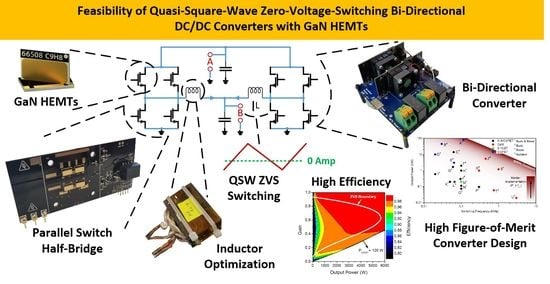
In this paper, the design of a 5.4 kW bi-directional DC/DC converter with QSW ZVS is implemented with GaN-based half-bridge prototypes with short circuit protection capability as proposed in [
15]. The converter utilizes two half-bridges to cancel out inductor current ripple so that output voltage ripple and capacitor equivalent series resistance (ESR) losses would be reduced [
14]. The rest of the paper is organized as follows.
Section 2 discusses GaN HEMTs in general and describes the selected GaN HEMT.
Section 3 explains the design logic of this study.
Section 4 gives the details and drawbacks of QSW ZVS.
Section 5 analytically expresses the design of high-frequency inductors and selection of filter capacitors.
Section 6 highlights the thermal performance for components in detail and presents the loss model and efficiency curves.
Section 7 discusses the operation range of the proposed converter and compares its performance with other proposed studies in the literature.
2. GaN HEMTs in Bi-Directional DC/DC Converters
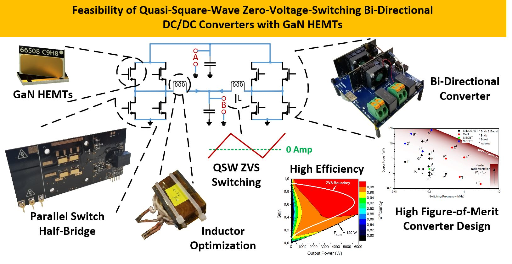
GaN HEMTs are superior devices in comparison to Si and SiC devices in terms of their high band gap, electron mobility, electric breakdown strength, and saturated electron velocity as shown in
Figure 1. These characteristics of GaN HEMTs result in lower conduction losses, higher switching speed, and devices of small size.
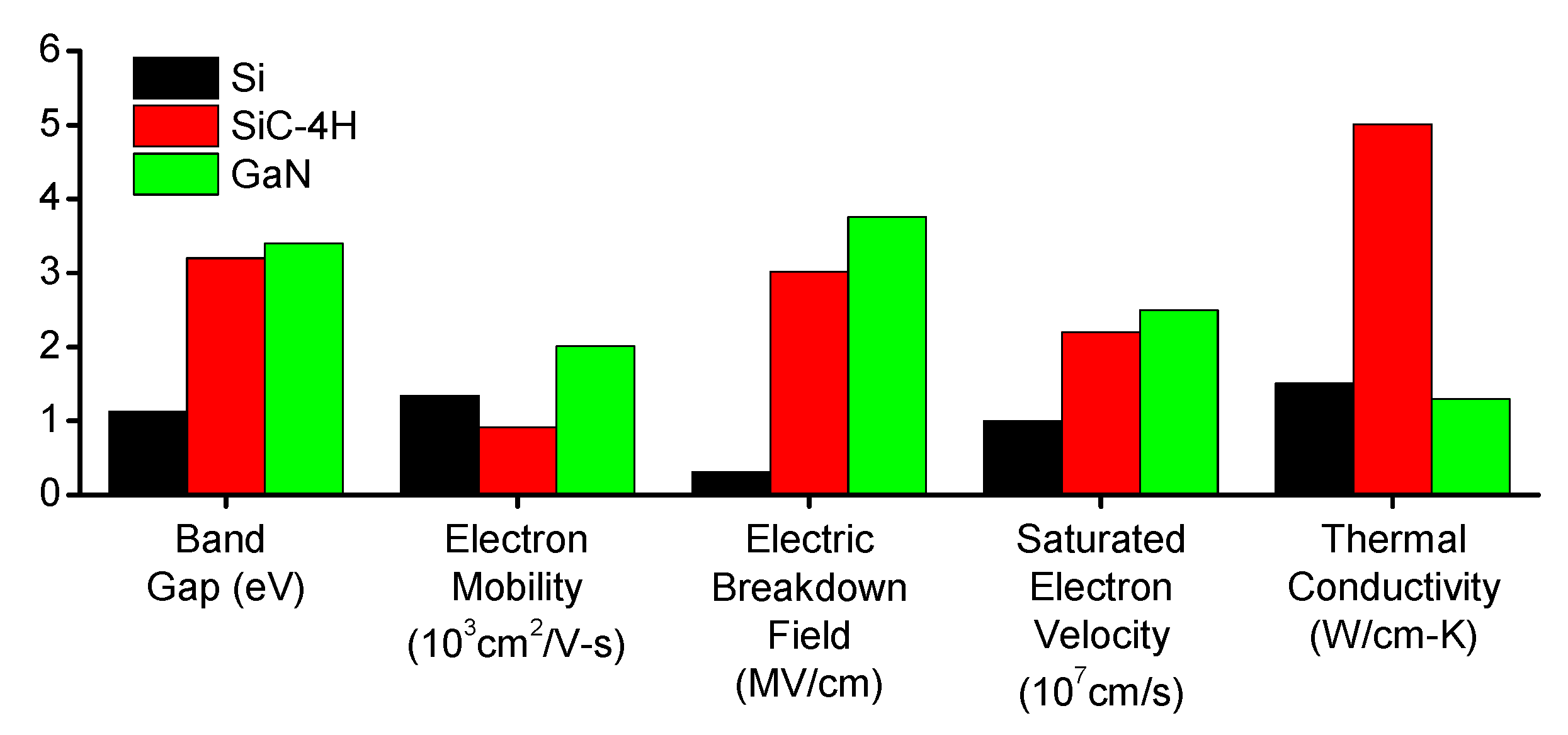
In comparison to P/N doped regions of Si-based MOSFETs, GaN HEMTs gain the conductivity by the piezoelectricity [
17]. As shown in
Figure 2, the Aluminum GaN (Al-GaN) barrier on GaN creates a region with free electrons which is called two-dimensional electron gas (2DEG). The p-doped gate controls the channel resistance by adjusting the charge density around the gate plate by controlling the electric field. The simple nature of GaN HEMTs allows for conduction in both directions without a PN junction. In other words, GaN HEMTs can conduct in the reverse direction without a diode, which eliminates the reverse recovery charge. Therefore, a synchronous DC/DC converter can operate without a reverse recovery loss.
A circuit model of GaN HEMT is presented in [
18] and shown in
Figure 3. The channel resistance of the conductivity can be modeled as a dependent current source which varies with gate bias, drain-source bias, and temperature. Moreover, the dynamic characteristic of GaN HEMTs gets important during switching transients. The voltage-dependent parasitic capacitors and in package inductances plays a significant role in the dynamic modeling of GaN HEMTs.
In the proposed design, a GaN HEMT, GS66508T is used where typical parameters are presented in
Table 1. By paralleling multiple devices, the equivalent on-state resistance can be decreased. However, the parallel connection of GaN HEMTs means increased turn-on, turn-off, and stored energy on the output capacitance. This results in increased switching losses especially for high power, high-frequency applications. In order to eliminate the switching losses, soft switching can be applied rather than hard switching. Soft-switching charges or discharges the output capacitance before switching transient and eliminates the power loss. Moreover, smooth transient of soft switching reduces
and
, so electromagnetic compatibility (EMC) standards can be followed much easily.
4. Quasi-Square Wave Zero Voltage Switching
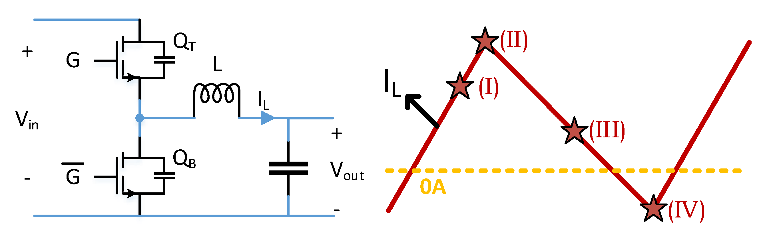
Quasi-square wave zero voltage switching (QSW ZVS) is an easy way to achieve zero voltage soft switching (ZVS) in Buck and Boost type DC/DC converters since it does not require any extra component, so decreases the reliability concerns. The ZVS is accomplished by inductive switching instead of capacitive switching. In capacitive switching, the transistor, which is supposed to be turned on in the next cycle, stays as charged to the DC link voltage level. Therefore, whenever it gets in conduction, the voltage on the output capacitance of the transistor has to be discharged which causes the switching energy dissipation and overshoot on the transistor current. However, in inductive switching, the voltage on the output capacitor of the transistor is discharged in dead-time by the load current and the transistor gets in conduction with zero voltage on itself. As a result, the energy is not dissipated during the switching transition.
An example is illustrated in
Figure 6 on a buck converter where the inductor current ripple is more than twice of output current; therefore, it goes below zero. Four moments are marked on inductor current in
Figure 6 where (I) is the charging moment, (II) is the moment when high side transistor (
) turns off and low side transistor (
) turns on, (III) is the discharging moment and lastly (IV) is the moment when
turns off and
turns on.
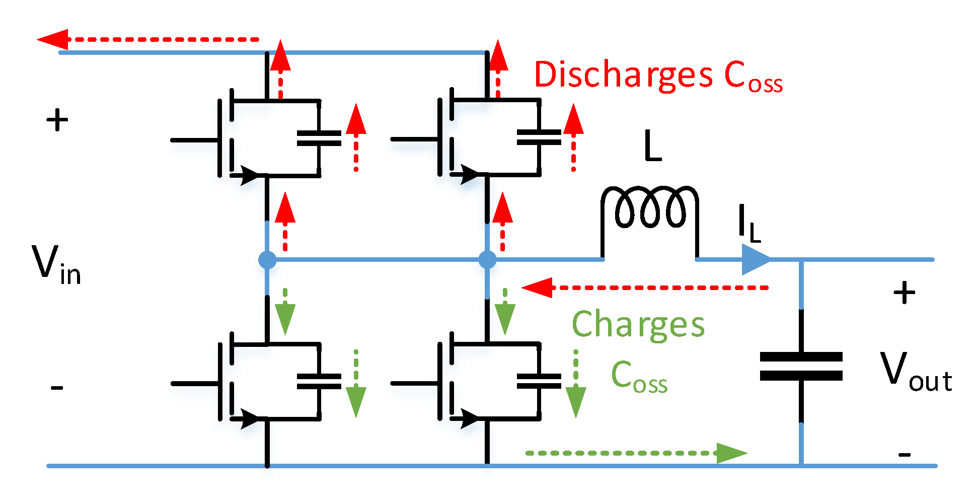
Since the inductor current charges and discharges the output capacitance of GaN HEMTs, the required dead time and negative current can be calculated. Due to the parallel switching operation applied in this design, the resonant current has to charge or discharge the output capacitances of both transistors in parallel connection. Therefore, the total output capacitance needs to be doubled compared to the output capacitance of a single transistor case. At the moment (IV), the inductor current which flows in a negative direction charges two GaN HEMTs and discharges two GaN HEMTs as presented in
Figure 7. According to the principle of conservation of charge, the required current or duration can be calculated as shown in Equation (
1) assuming that the inductor current is constant during the dead time period. The required minimum dead time (
) can be calculated with the discharging inductor current (
), total discharged capacitance in the half-bridge (
) and its voltage level (
). For a configuration that operates under 400 V DC bias and with 4 A of inductor current flowing in the reverse direction, a dead time of 40 ns is required as a minimum to achieve zero voltage switching. Considering the gate charge and discharge duration, 100 ns of dead time would be suitable and safe for this design.
The parallel-connected bridge structure is tested on a simulation platform with 100 ns of a dead-time period. The results show that the high side switch, i.e., the control switch for buck mode, turns on with zero voltage switching as shown in
Figure 8. Since the inductances are included in the simulation model, tiny oscillations are observed on the channel current (I
ds). However, the oscillations, which can cause extra power loss or terminal voltage (V
ds) overshoot, are damped strongly thanks to smooth current and voltage transitions prompted by the soft-switching. This fact is the basis of easy implementation of a parallel device structure in ZVS converters.
5. Design and Selection of Passive Components
As discussed above, quasi-square wave zero voltage switching suffers from a high current ripple. Besides the thermal stresses over the capacitors and inductors, the current ripple also causes the output voltage to swing unless the filter capacitors are chosen adequately. Instead of applying all current ripple to the output filter capacitors, interleaving the multiple numbers of bridges could help to decrease the ripple. Moreover, the thermal stress per bridge decreases as well.
The proposed converter can operate in buck and boost modes. The nominal operating conditions are given in
Table 2 for each mode. Based on these operating conditions, the number of the interleaved bridge is selected for theoretical and practical reasons. Theoretically, the number of interleaved bridges is evaluated and compared as shown in
Table 3. Since buck and boost modes operate with almost complementary duty cycles, a minimum ripple is obtained for the same number of bridges. Interleaving three bridges is the most suitable option for buck and boost modes in terms of ripple cancellation. However, the transferred power per bridge decreases with an increasing number of bridges. In other words, the increased number of bridges decreases the utilization of filter inductors and switches if the output power is considered constant. As a result, interleaving two bridges seems to be the most advantageous case for handling the ripple while maximizing the power density.
5.1. Inductor Design
The inductor design is one of the most critical steps for the QSW ZVS converter because the increased current ripple can saturate the magnetic core and cause lots of heat dissipation. The total inductor loss (
) can be estimated by summing winding losses (
) and core losses (
) as shown in Equation (
2). Firstly, the winding losses can be split into two parts: the DC losses and AC losses. The DC losses can be calculated with the average inductor current (
) and winding resistance (
). However, for an inductor with multiple numbers of layers and thick wires, AC loss dominates due to the eddy effects in high-frequency applications. Therefore, the thickness of the wire should be selected by taking the skin depth into account. Then, the equivalent AC resistance of the inductor can be found by multiplying the winding resistance by a frequency-dependent coefficient (
). As a result, the AC winding losses can be calculated with the magnitude of the inductor current ripple (
) and equivalent AC resistance. The total winding loss equation is presented in (
3). Secondly, the varying flux density in the magnetic core creates hysteresis losses and heats the magnetic core. In order to calculate the core loss, the specific power loss (
) which depends on the AC magnetic flux density (
) and switching frequency (
) can be multiplied by the core volume (
) as given in (
4).
In this design, the switching frequency is selected as 450 kHz and the inductor should carry 10 A on average with 28 A peak-to-peak ripple as given in
Table 4. The skin depth for 450 kHz is 97.2
m, so a Litz wire needs to be used to handle the ripple. A Litz wire with 400 strands of 80
m of thickness is chosen.
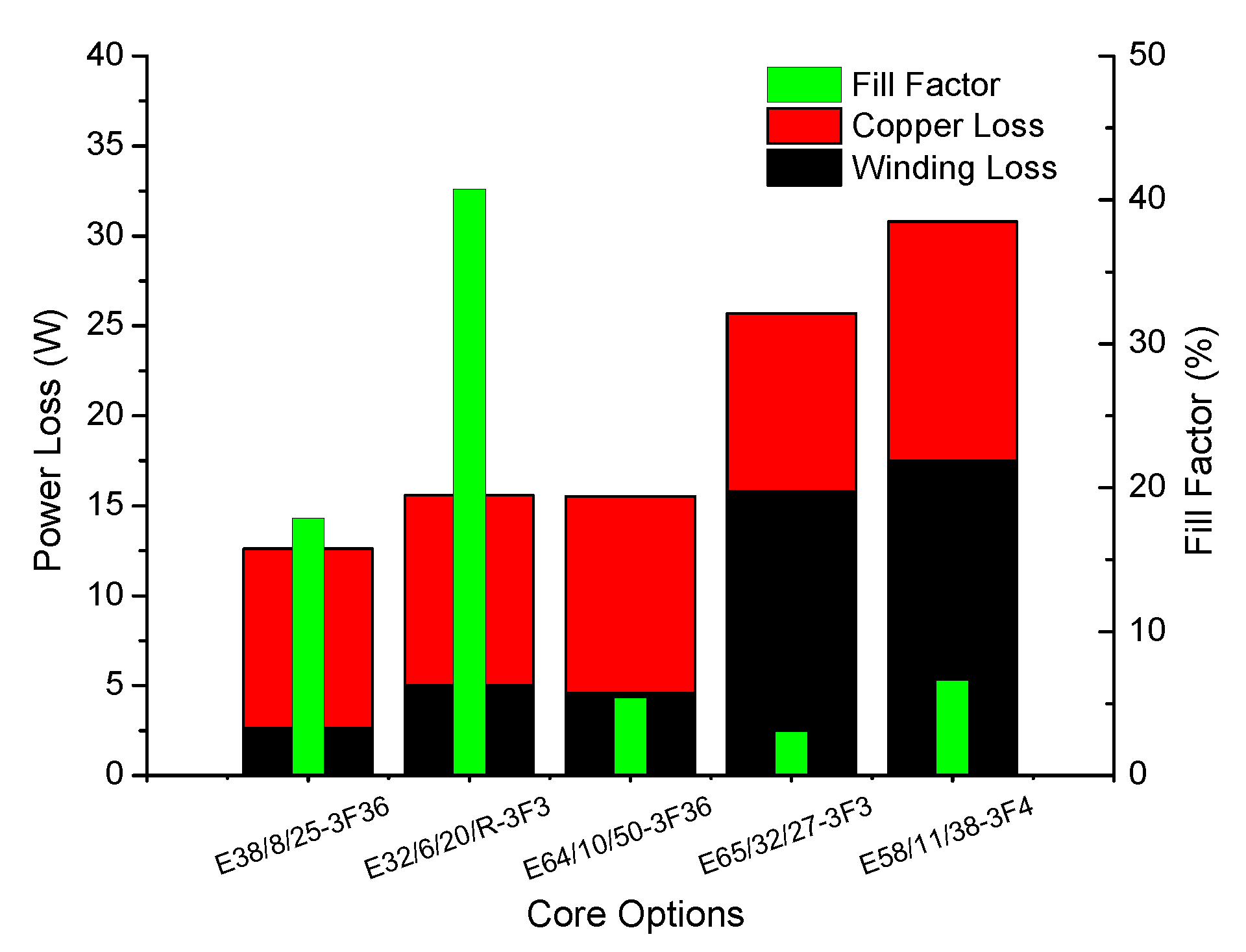
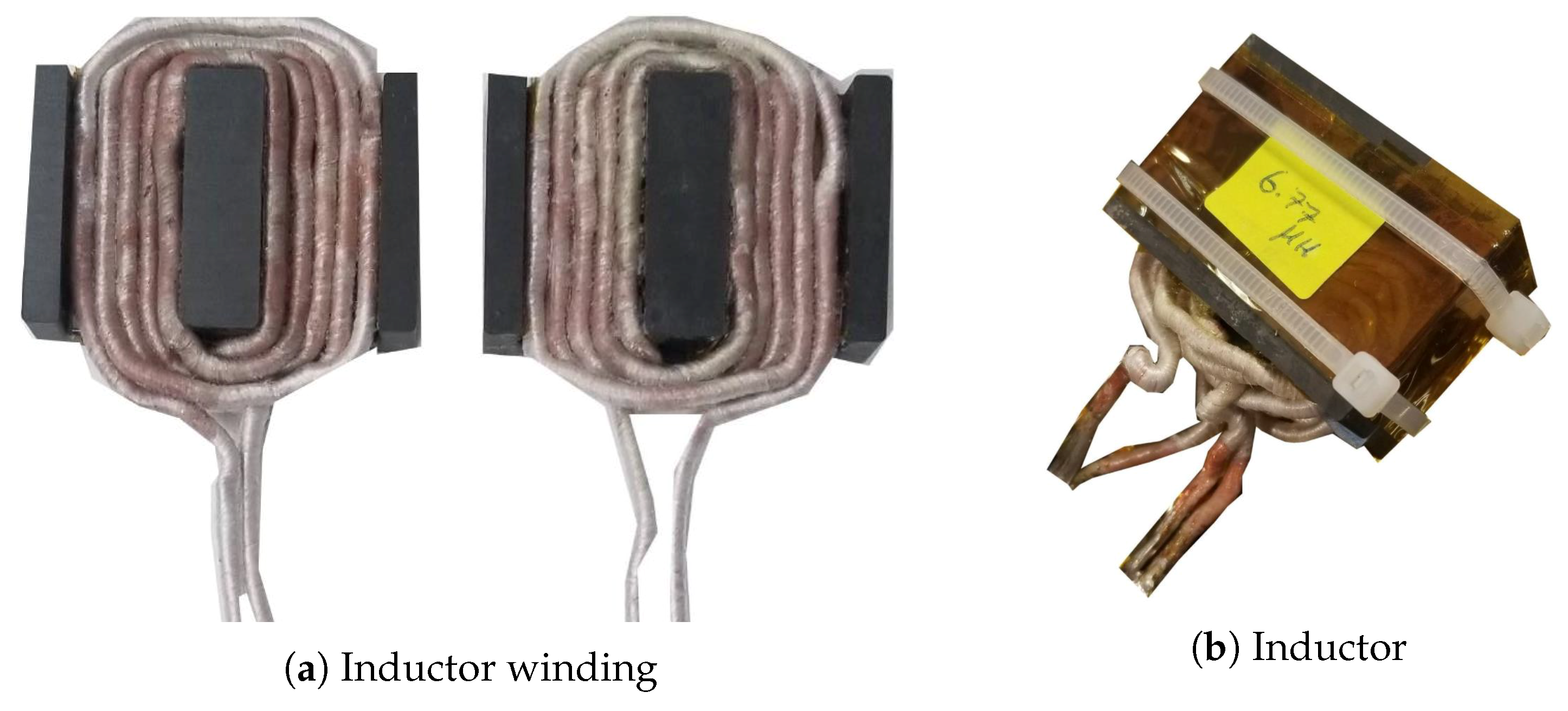
Off-the-shelf magnetic-gapped E cores are not suitable for this application due to their low saturation current rating and high core loss density. Therefore, a gap-less E core is used and the air gap is adjusted with a few pieces of isolation papers such that the magnetic field density and number of turns can be optimized. Another important measure for the inductor is the power loss caused by the current. For this purpose, the DC resistance of the winding and alternating current (AC) resistance are calculated. In addition to winding loss, core loss is calculated with the given specific power loss in the magnetic core datasheet. The specific power constant increases sharply with increasing AC magnetic flux density and frequency. The total power loss is compared for different magnetic cores and fill factor as presented in
Figure 9. The magnetic core E38/8/25-3F36 [
21] has the lowest core and winding losses. It has a fill factor of less than 20%, so it is suitable for paralleling two Litz wires so that the winding loss could be halved. The final loss of E38/8/25-3F36 can be reduced down to 7.6 W. The wounded magnetic core is shown in
Figure 10a where two E cores will be placed on top of each other and wires will be paralleled and the final view of the inductor is presented in
Figure 10b.
5.2. Filter Capacitor Selection
The filter capacitor selection is critical due to fact that the capacitors have a limited lifetime. Therefore, the reliability of converters is strongly dependent on the capacitors especially connected to DC link terminals. The selected capacitor type and the applied stress on those capacitors should be considered wisely. In order to reduce the ripple stress and have high efficiency, interleaving is mainly used as in [
22,
23].
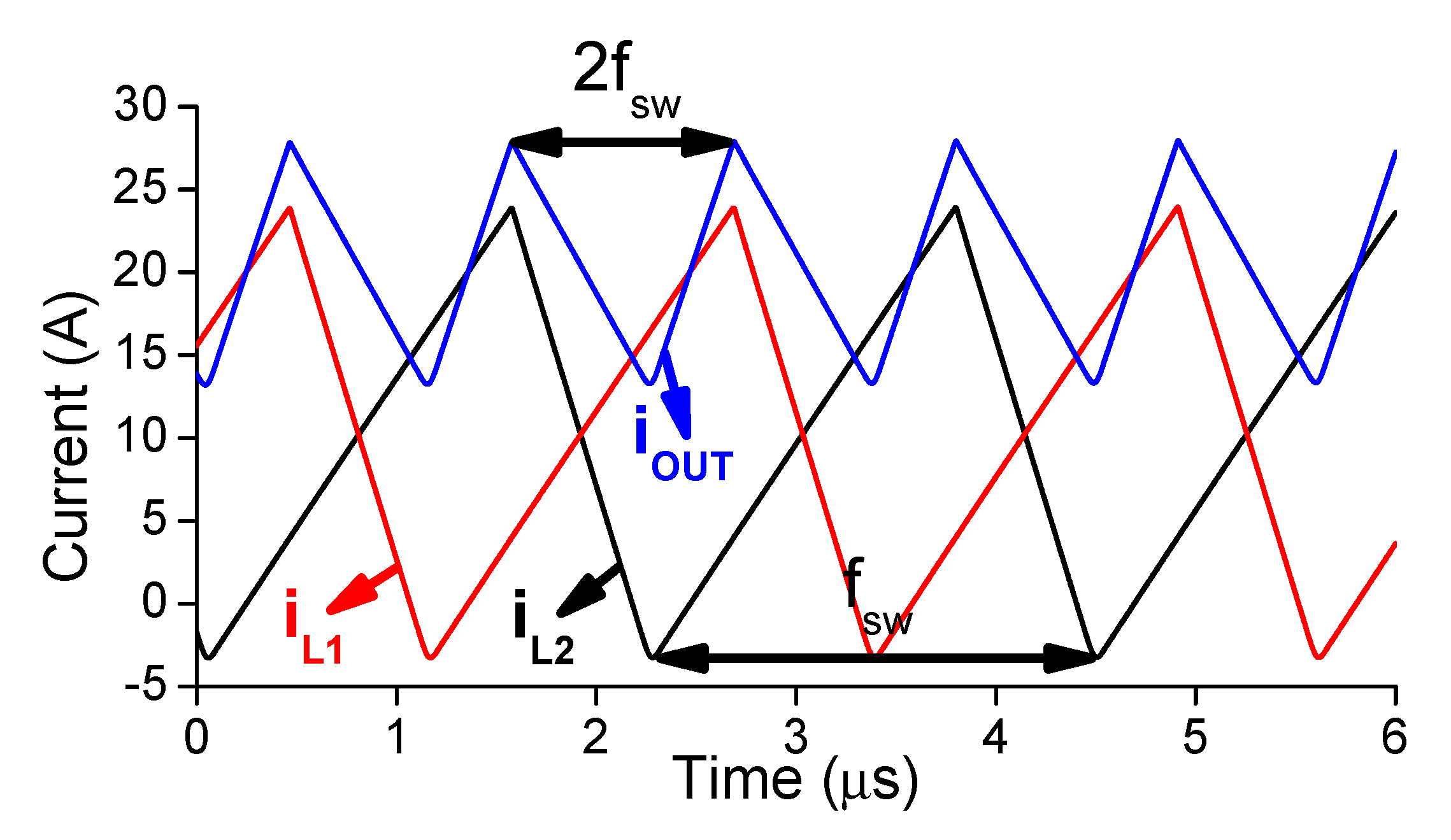
On the one hand, interleaving half-bridges reduce the current ripple for the output and input capacitors. On the other hand, the frequency of filter capacitor current increases as much as switching frequency times the number of interleaved bridges. Therefore, for two interleaved bridges, the filter capacitor carries the current with double switching frequency. The simulation result presented in
Figure 11 shows the inductor currents and the output current for the rated buck mode of operation. The ripple reduction on the output current with respect to the input current can be calculated as in (
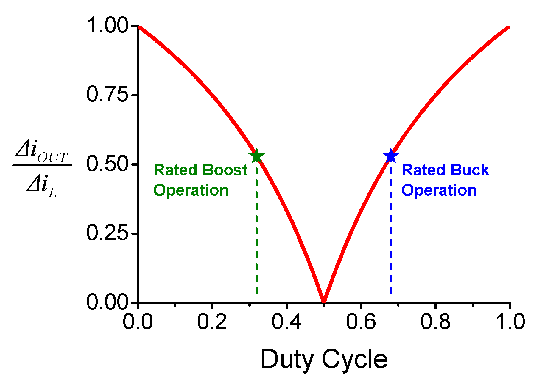
5). The ripple cancellation is symmetric with respect to the 0.5 duty cycle due to two interleaved bridges as presented in
Figure 12. Based on the analytical and simulation results, the amplitude of the ripple current is almost halved and the frequency is double switching frequency, 900 kHz.
In order to achieve a 1% output voltage ripple, the output filter capacitor should be at least 690 nF according to Equation (
6). This calculation is valid only for an ideal capacitor and ideal connections. However, capacitors are not ideal and have parasitic inductances and resistances. Therefore, the frequency response of the filter capacitor gets important since it should carry a considerably high amplitude of ripple current at 900 kHz. Moreover, the dissipation factor has to be low enough to keep capacitors thermally safe.
Even though the aluminum electrolytic capacitors are dense in terms of capacitance per volume, their temperature sensitivity and equivalent series resistance (ESR) value are high [
25]. Besides their low lifetime, the parasitic inductance of electrolytic capacitors makes them unfeasible for this application due to the increased frequency of current ripple. However, the film capacitors have low ESR and parasitic inductance and their capacitance and dissipation factor is almost the same over a wide temperature range [
25]. Thanks to the low capacitance requirement of the proposed converter, the film capacitors in small volumes can be utilized. Moreover, the film capacitor’s open circuit characteristics under a fault increase the reliability of the overall system.
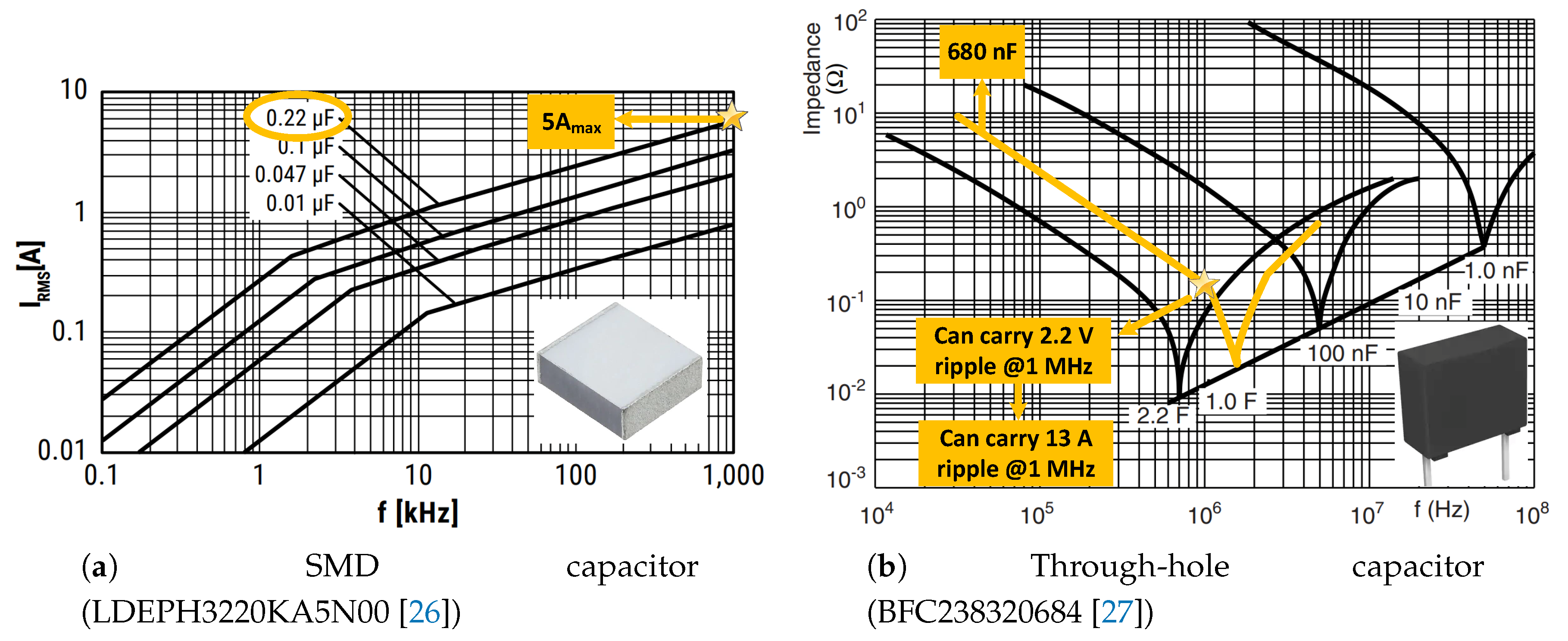
The RMS value of the output capacitor current is 4.2 A at 900 kHz for rated operation as calculated as in Equation (
7). In order to filter out this current, two surface mount design (SMD) film capacitors, LDEPH3220KA5N00 [
26], and one through-hole (TH) film capacitor, BFC238320684 [
27], are used.
Figure 13a,b shows the current-carrying capability of SMD and TH film capacitors, respectively. The total capacitance is 1120 nF and the current range goes up to 23 A which is higher than the required value. Both capacitors are rated 630 V as maximum.
In comparison to the output capacitor current, the relationship between the inductor current and the input capacitor current is more complicated. Since the inductor current ripple is supplied by the input capacitor only for the ON period of the high side switch, the ratio is not direct. Nevertheless, in order to estimate the stress over the input capacitor better, the analytical equation in (
8) is derived where the RMS value of the input capacitor current (
) can be expressed with duty cycle (
D), inductor current ripple magnitude (
), the minimum and maximum values of the inductor current (
,
). It is calculated as 6.2 A for rated operation.
The stress over the capacitors can be identified by extracting frequency-dependent equivalent series resistance (
ESR). Then, the total capacitor loss can be calculated as given in (
9). Note that, each terminal has the same capacitor configuration.
6. Experimental Results
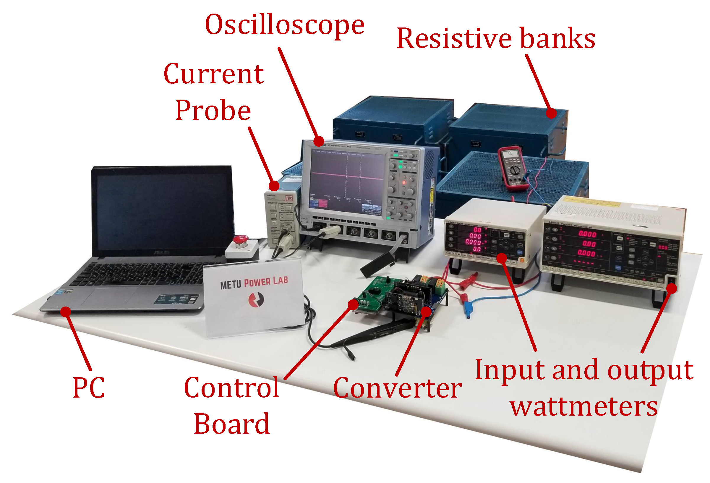
The bi-directional DC/DC converter is physically implemented and tested under full load for both buck and boost modes with the presented experimental setup in
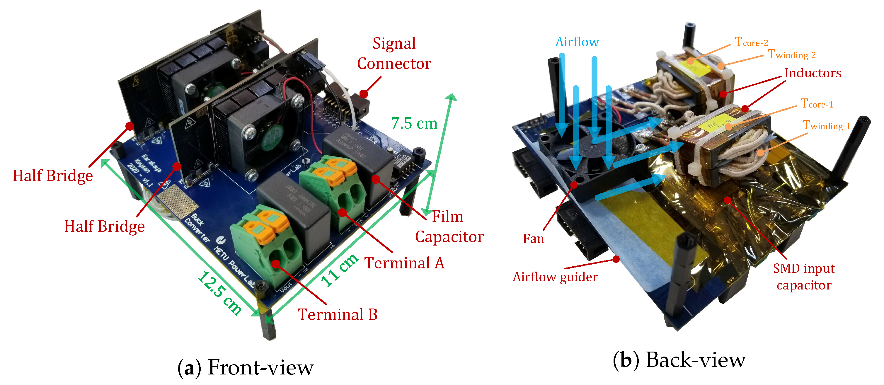
Figure 14. Converter dimensions are 7.5 cm, 11 cm, 12.5 cm as shown in
Figure 15a which results in 5.24 kW/
L power density at full load. During the experiments, all waveforms are recorded by a digital oscilloscope, Waverunner 44xi (Teledyne LeCroy, New York, USA) and the current waveforms are measured by a current probe, TCP305A (Tektronix, Bracknell, UK). Resistive banks are connected in parallel as load. Input and output powers are measured by watt meters.
GaN HEMTs with their fast switching capability are subject to circuit noises caused by high
and
. In order to eliminate the risk of a shoot through short circuit failure, a short circuit protection method is proposed in [
15] and applied on the half-bridge boards as presented in
Figure 16. The half-bridge is designed with a parallel structure to increase the current carrying capability and well-suited for the proposed converter.
6.1. Thermal Tests
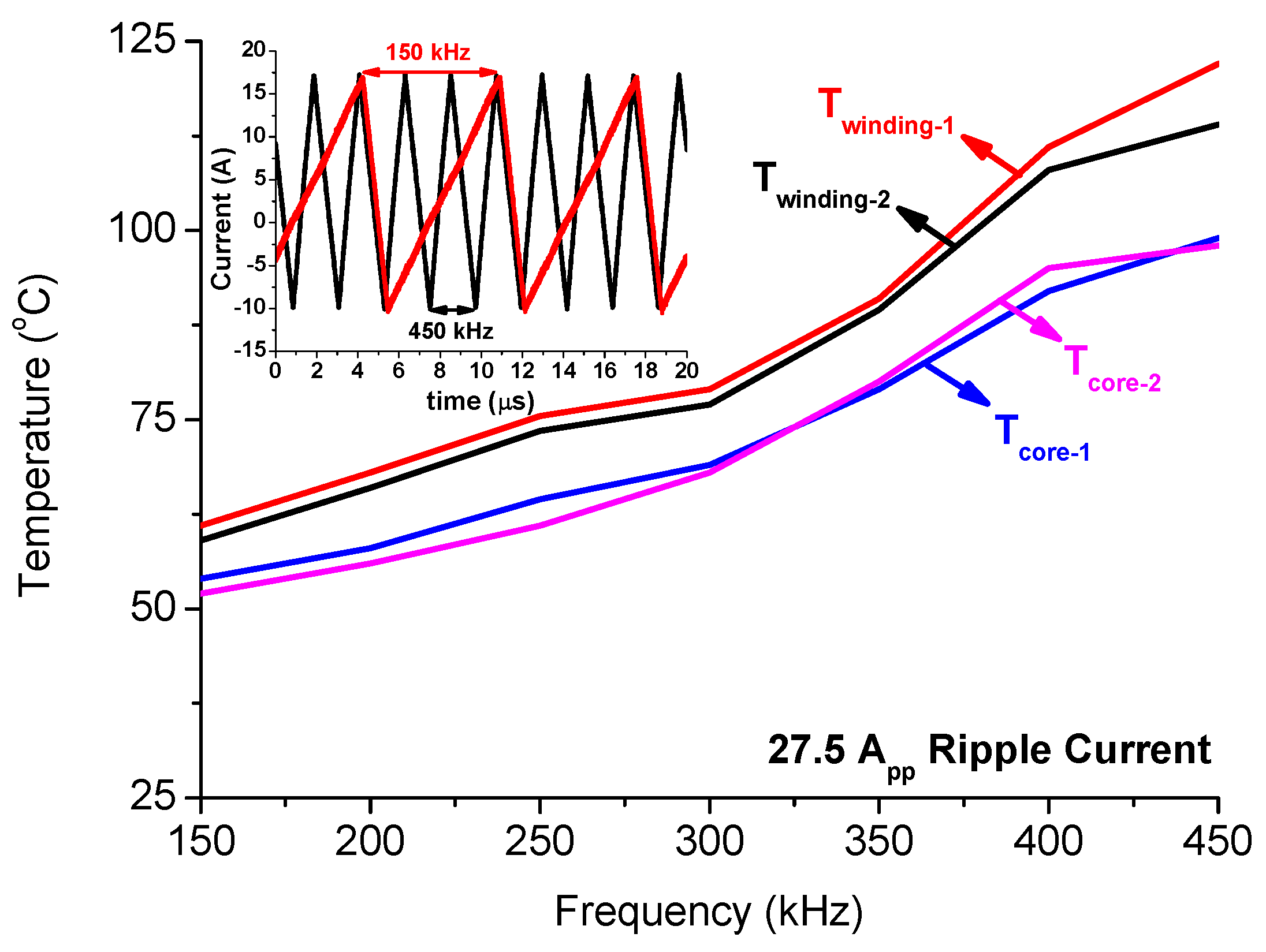
The thermal resistance of the magnetic core of the inductors is not presented clearly in the datasheet. Therefore, the thermal design has to be verified before applying full load. The thermal stresses of the inductors are dominated by the AC winding losses and the core losses which both are affected by the switching frequency. In order to see the effect of switching frequency, the rated ripple amplitude of the current with varying frequency is applied to the inductors to see the cooling performance.
Thermal measurement points are presented in
Figure 15. The input voltage and duty cycle are adjusted so that always the same amplitude of current flows through the inductors at different frequencies. The operating frequency is changed from 150 kHz to 450 kHz with 50 kHz steps and the current waveforms were recorded by the oscilloscope as shown in
Figure 17 for the minimum and the maximum frequencies. During this phase of the thermal tests, the cooling fan shown in
Figure 15b is not active and natural cooling is applied. The resulting temperatures are given in
Figure 17 where the maximum temperature increases up to 122 °C at windings and the ambient temperature is 25 °C. Note that, in this study, all thermal results are measured after 30 min of operation.
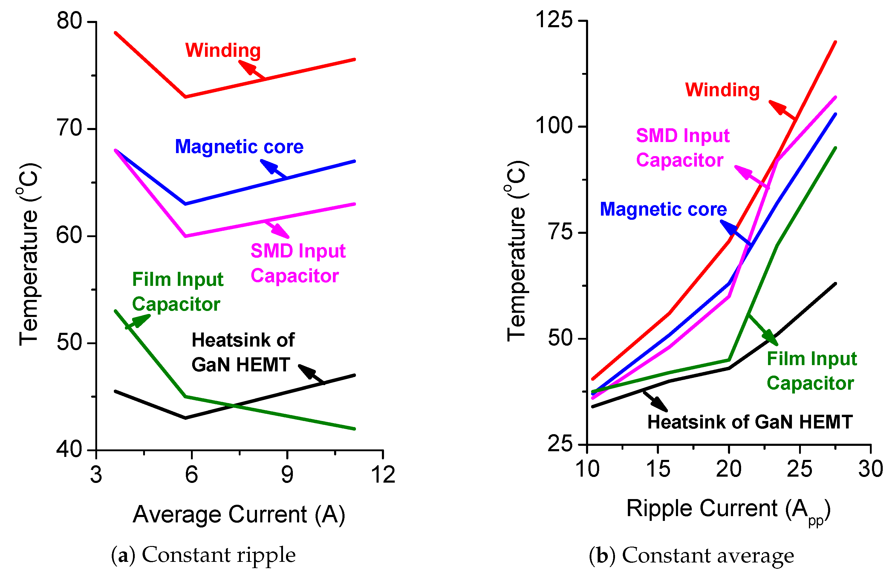
Moreover, it is important to see the effects of the current ripple and average separately to figure out the main reason behind the heating of passive components or GaN HEMTs. For this purpose, two test sets are performed. Firstly, the average of the inductor current is changed while the ripple magnitude of the current stays the same, and secondly, the average of the inductor current is kept constant while the ripple changes. The results of these two experiments are shown in
Figure 18a,b. The temperature is recorded for five different components, the inductor winding and the core, heat sink of GaN HEMTs, and input capacitors.
Figure 18a shows that the effect of the change in the average current is limited, but the current ripple is more dominant on the heat loss as given in
Figure 18b. This outcome can be considered as a natural result of the proposed converter where a high current ripple is utilized to reach zero voltage switching.
Considering the F class winding, curie temperature of the magnetic core which is around 220 °C, the E class SMD capacitors and A-class through-hole capacitors, in order to guarantee a safe operation for passive components under full load, a fan is used, without reducing the power density, to limit heating. This configuration is presented in
Figure 15.
Table 5 gives how the fan affects the temperatures of the components. As expected, it significantly reduces the temperature of the inductor and surface mount device (SMD) input capacitors which are on the same side as the fan. This also shows that the passive components’ thermal classes are compatible with the further increase in ambient temperature.
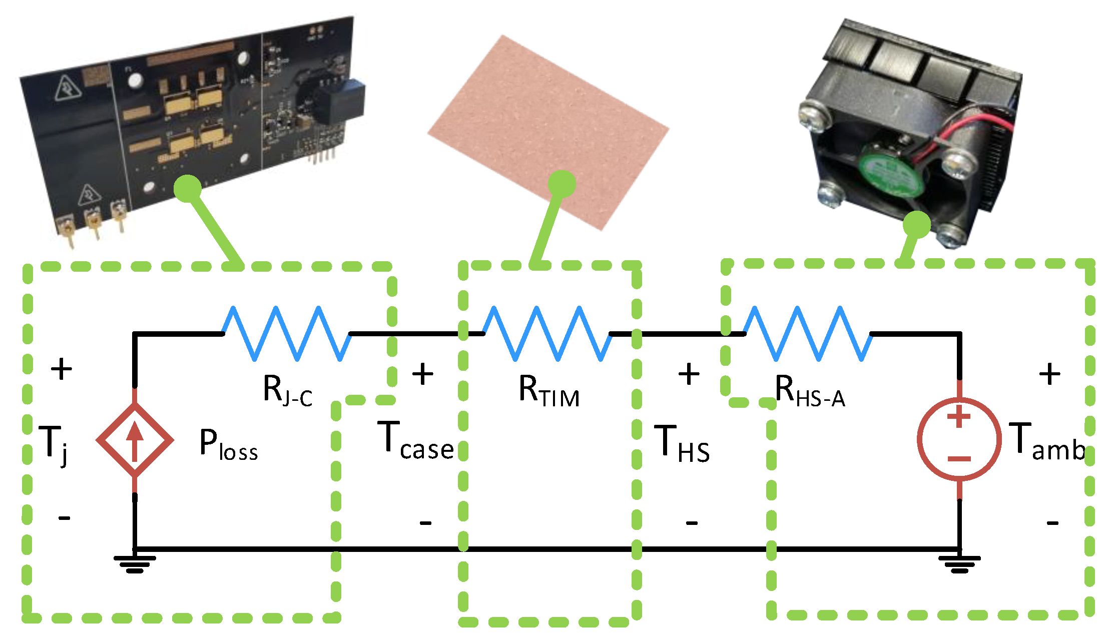
Lastly, the junction temperature of GaN HEMTs can be estimated by solving the thermal circuit presented in
Figure 19. The paralleled GaN HEMTs on the half-bridge board are connected to the same heat sink to cool down. In order to inhibit the short-circuit risk of low and high side switches, an electrically isolated thermal interface material (A10092-01) with 3.5 °C/W is used. The low profile heat-sink (APF40-40-10CB) is connected to the half-bridge board and a fan (OD3510-05MB). The heat-sink and fan pair results in 2.5 °C/W thermal resistance. Then, it is possible to estimate the junction temperature if the power loss is known. For this purpose, the losses extracted from the simulation results are taken as the reference. The losses of the GaN HEMTs over a half-bridge are estimated as 19.1 W where the average and ripple current of the inductors are 10 A and 27.5 A
PP, respectively. Then, the junction temperature can be estimated by (
10).
6.2. Buck and Boost Modes
The buck and boost mode tests are conducted at the same voltage ratings for varying load power. For buck mode, the operating point is selected as 400 V to 270 V conversion and for the boost mode, it is vice versa.
During the tests, the loading is increased by 15% in each step. The temperature on critical components is recorded so that the thermal performance could be verified under rated operating conditions. The change in the temperature is shown in
Figure 20 for a varying load current range. As expected magnetic core has the same losses for buck and boost mode operation because the inductor current is the same. The measured and estimated heat-sink temperatures vary 5 °C. By solving the thermal circuit presented in
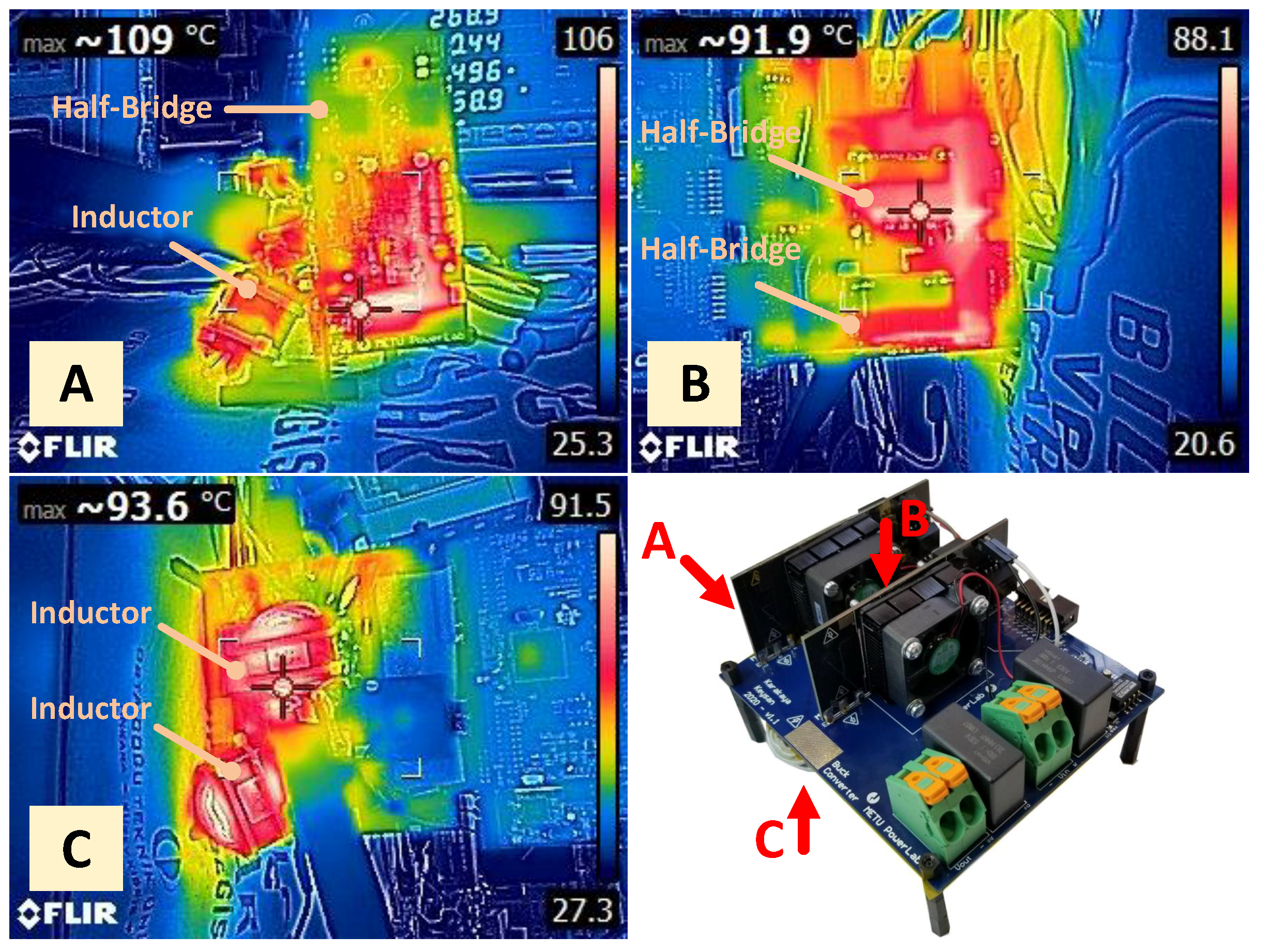
Figure 19, the junction temperature of GaN HEMTs is estimated. The estimated junction temperature for buck and boost mode operations is 131 °C and 137 °C, respectively. Considering the maximum allowed junction temperature of GaN HEMTs (150 °C), the transistors operate at the safe-operating-area boundary. The temperature on the converter board is recorded under full load and presented in
Figure 21. The hottest points on the half-bridge board, heat-sink, and inductors are marked.
Moreover, the output voltage ripple is measured as shown in
Figure 22 for full load condition. The output voltage ripple gets affected by the duty cycle, frequency, and input voltage. Since these three parameters are the same for all load ranges, the output voltage ripple is constant over the load current for both operating modes. According to the experimental results, the output voltage ripple swings 2.3 V in buck mode and swings as 3.9 V for boost mode which are less than 1% of the average output voltage.
6.3. Loss Model and Comparison
In order to identify the loss sources, an analytical model is constructed. The losses on the passive components can be calculated as explained above. Moreover, the losses on GaN HEMTs are split into two parts: conduction and switching losses. In order to calculate the conduction loss on a half-bridge, four GaN HEMTs in this case, the phase current (
) can be used which is formulated as in (
11). Then, the conduction loss can be calculated by multiplying the halved on-state resistance (
) due to paralleling as presented in (
12). Moreover, the switching loss can be found by (
13). The turn-on energy (
) and turn-off energy (
) of a single device half-bridge are characterized by using the simulation model. Lastly, due to the high ripple current, the ohmic losses on the printed circuit board (PCB) traces and connectors get also important which can be calculated as similar to GaN HEMTs’ conduction loss. Assuming that the PCB has the same resistance (
) between (+) node to phase and (−) node to phase, the trace loss can be equated as given in (
14). In summary, the analytical loss model finds out the conduction and switching losses on GaN HEMTs, the winding and core losses of the inductors and the losses on the filter capacitors, and the trace losses as well.
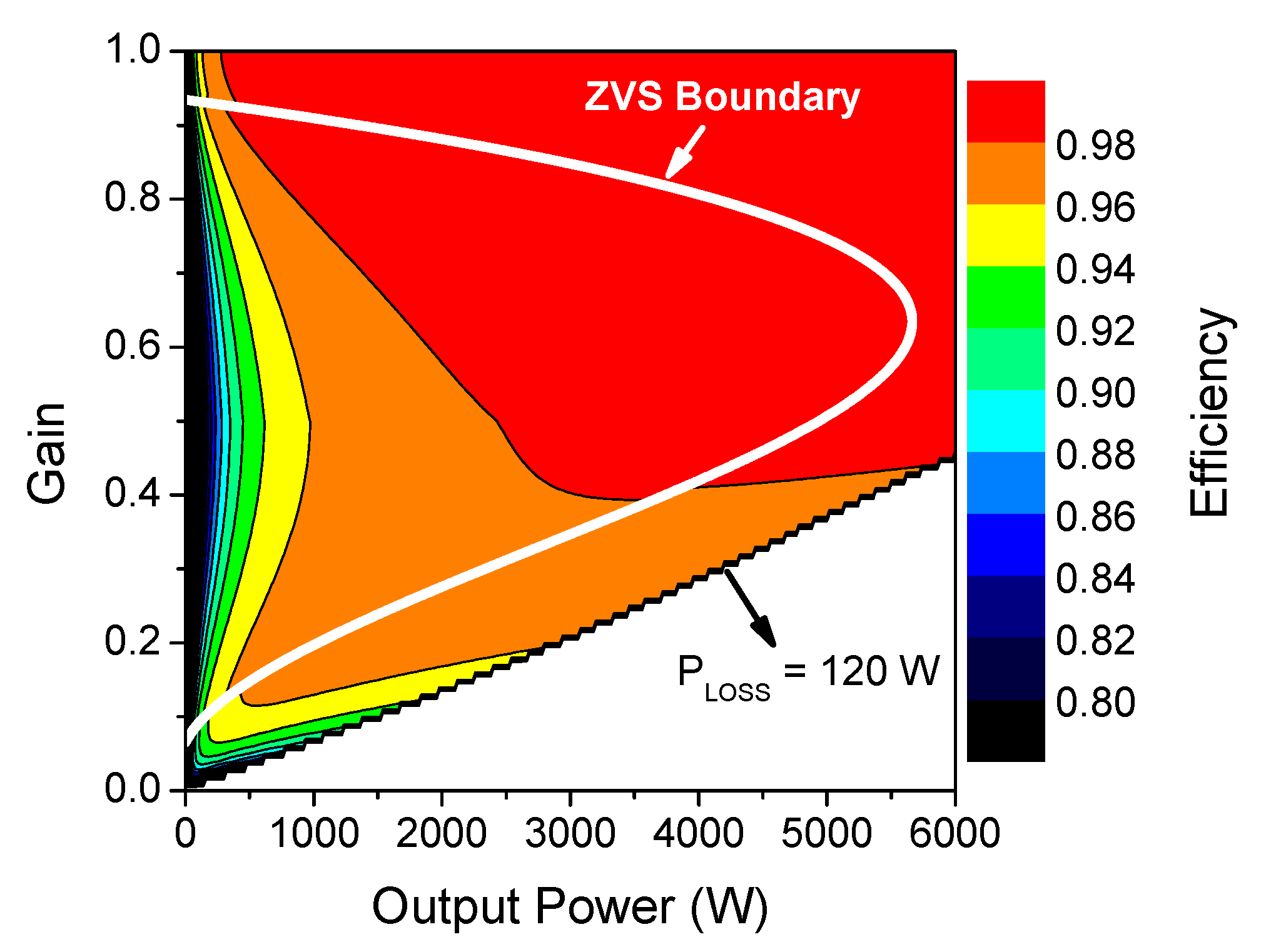
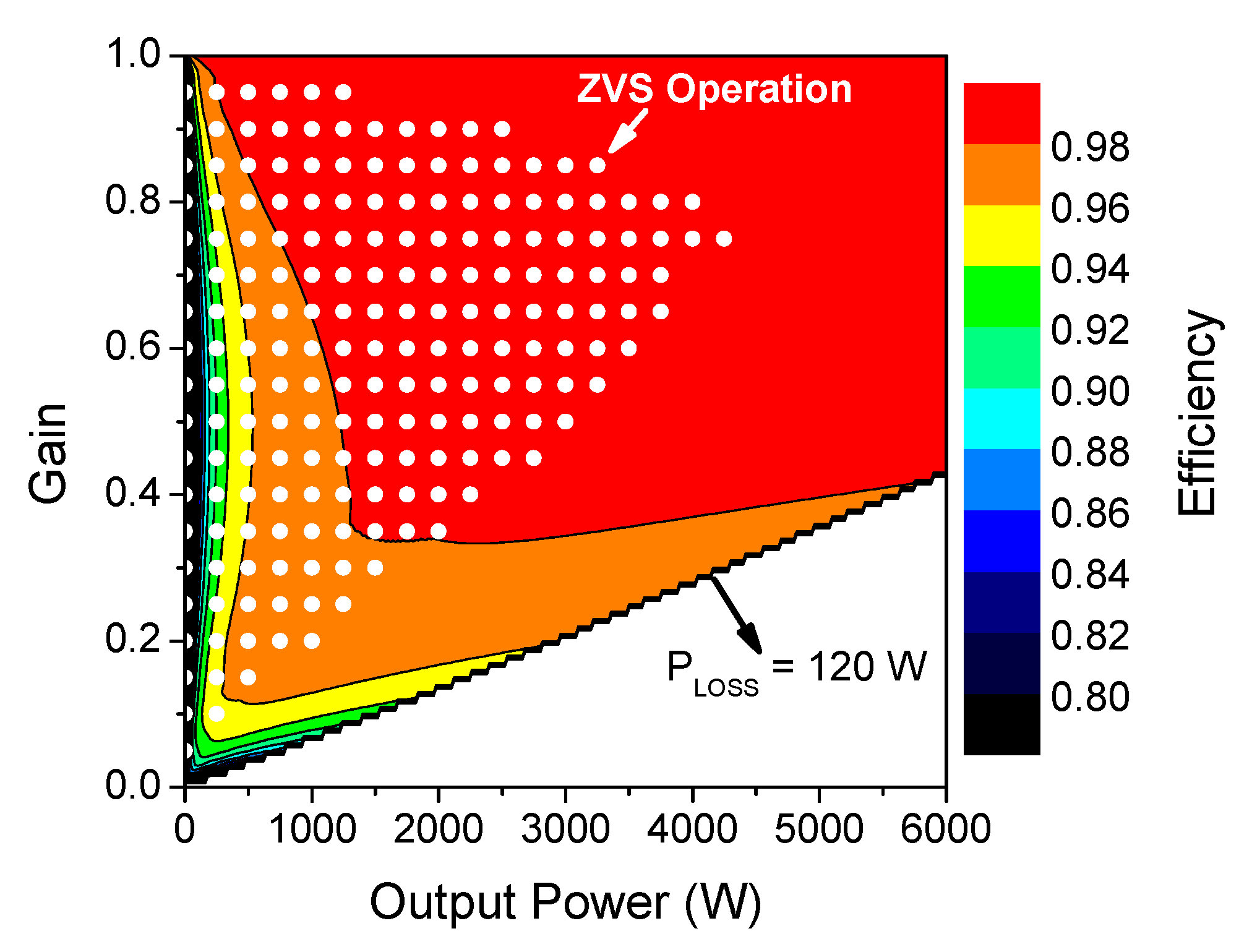
The operating range of the proposed converter is analyzed in
Figure 23 by using the constructed loss model. The maximum allowed loss is 120 W due to the cooling capability of the converter. The ZVS boundary is also plotted in
Figure 23 by using Equation (
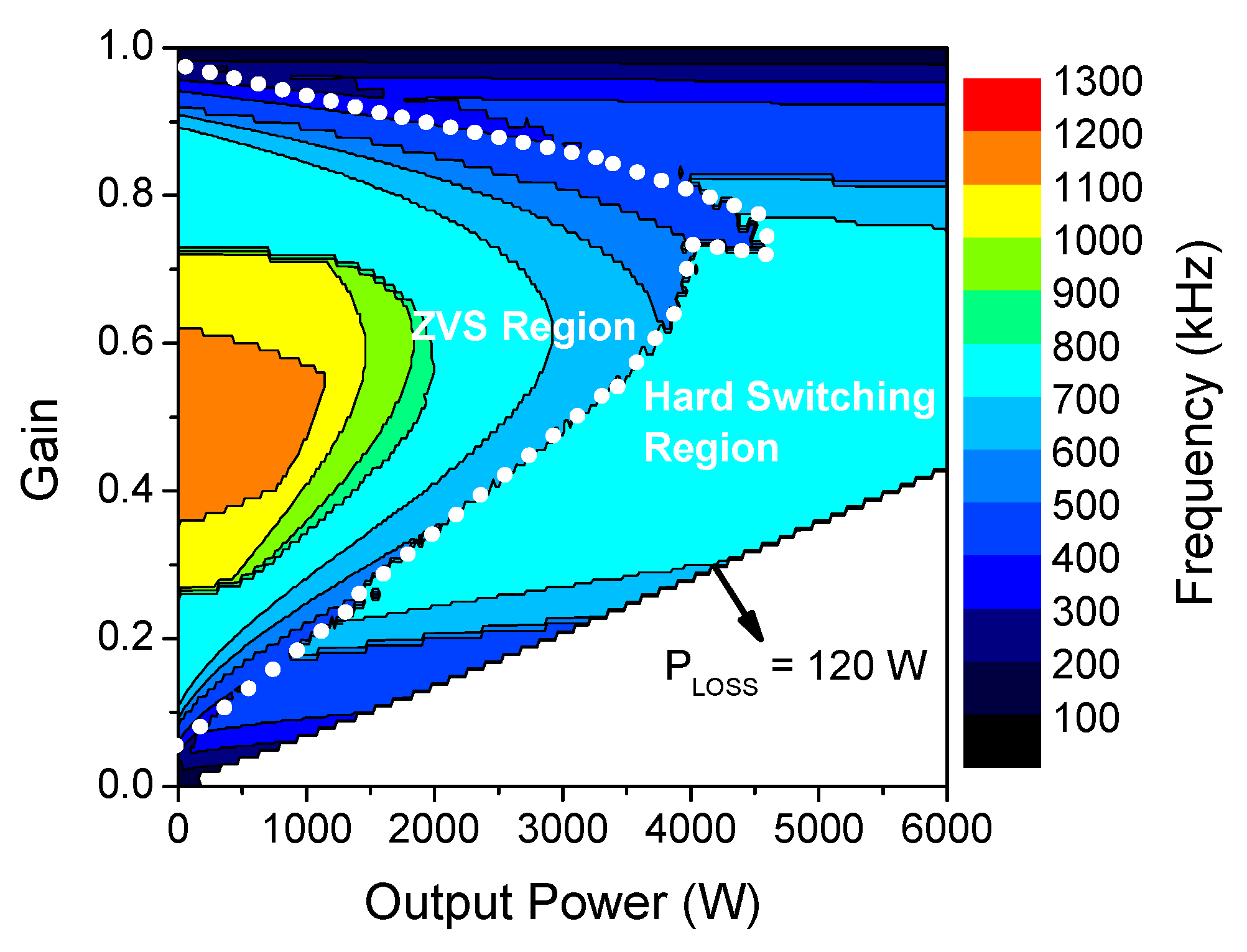
15). Here the ZVS condition is determined as a drop in the inductor current down to −4 A. The converter is able to operate with an efficiency higher than 90% at almost all operating points where the efficiency is higher than 95% for a region larger than half of all operable points. However, a constant switching frequency does not give the optimum performance for all operating points. Therefore, a frequency sweep is applied from 100 kHz to 1.5 MHz for each operating point and the switching frequency with the minimum loss is picked for that operating point as presented in
Figure 24. Having frequency as a control parameter improved the efficiency performance of the converter as presented in
Figure 25. As a result, the efficiency of the converter stays higher than 96% for a very wide operating region. This result highlights the effect of switching frequency to balance and to minimize the losses.
Figure 24 and
Figure 25 show the converter does not always give the best performance for ZVS operation contrary to the popular myth that a soft-switching will increase the efficiency by eliminating the switching losses on GaN HEMTs. The QSW ZVS operation requires a high inductor current ripple, so it increases the inductor losses and the conduction loss of the GaN HEMTs. Therefore, in order to get the maximum efficiency, the converter might be operated at a higher switching frequency. Even though the switching loss increases, the increase in the frequency decreases the current ripple and it eliminates the high conduction loss caused by the ripple. However, depending on the requirements of the application, a low frequency might be preferred to get a ZVS operation. The lower EMI radiation of ZVS operation with slower current and voltage transitions might be advantageous.
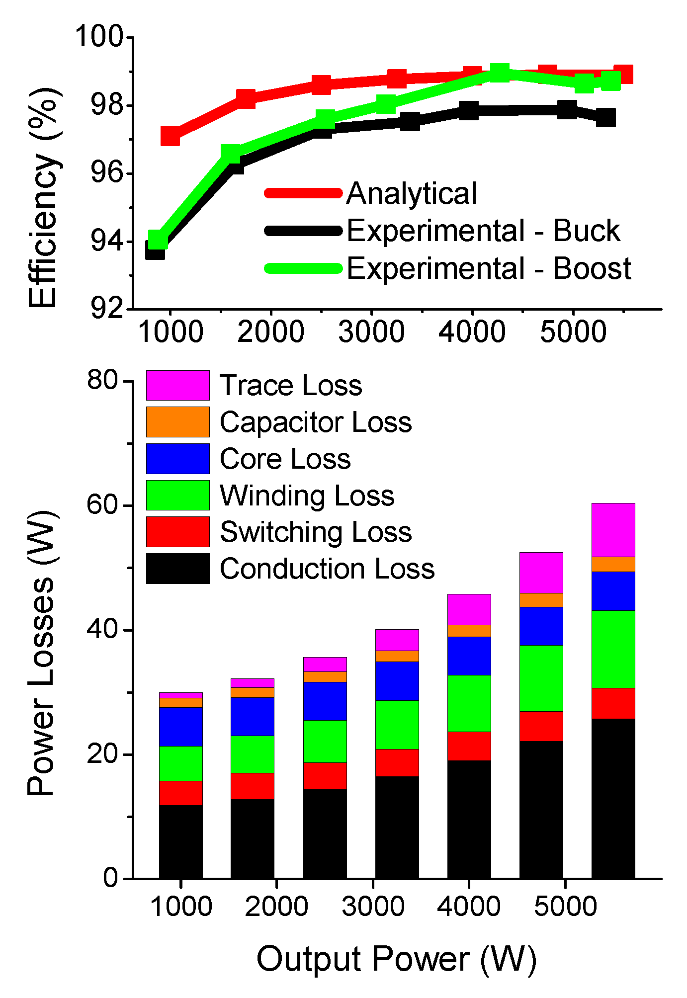
Lastly, the analytically-calculated losses are presented and compared with the experimental results in
Figure 26 where the operating point sweeps from 1 kW to 5.5 kW under 400 V of input voltage and 450 kHz of switching frequency. Analytical efficiency is slightly higher than experimental results due to unconsidered loss sources and the measurement error of the experimental results. The conduction loss on the GaN HEMTs is the most dominant loss source due to the high ripple of the current and it verifies the requirement of device paralleling. Moreover, the one-layer design of the inductor with litz wires helps to significantly reduce AC losses on the inductor.
7. Discussion
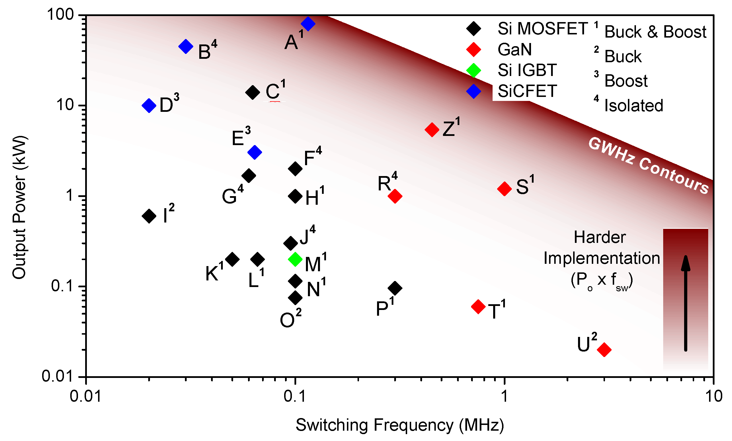
The DC/DC converters with different topologies and devices are compared in
Figure 27. The presented converters include bi-directional converters, uni-directional buck or boost converters with soft-switching, and isolated converters. The detailed specs of the converters are presented in
Table 6. MOSFET is the most common semiconductor used in these converters; however, SiC and GaN switches have an increasing trend in the last years. Furthermore, in
Figure 27, color contours are plotted where the color gets darker for increasing output power and switching frequency multiplication. With respect to the figure-of-merit (FOM) of the device (Q
g × R
ds-on), converters position for different power and frequency ranges. High voltage ratings of SiC and its lower losses in comparison to Si-based devices make SiC devices suitable for high power applications where the switching frequency varies from several tens of kHz to 100 kHz. On the other hand, GaN devices are located in a high-frequency region (>100 kHz) and power ratings less than 10 kW. This is due to the ultra-fast switching capability of GaN HEMT challenges high power applications with strong EMI noises. Moreover, the GaN HEMTs on the shelf have voltage ratings around 600 V which indicate that GaN HEMTs are not as feasible as SiC devices for high-power applications. Lastly, Si-based devices are mainly used for applications with easier ratings. The mature structure of Si devices and their considerably lower cost make them attractive for applications with affordable demands.
The
Figure 27 also gives a comparison for different topologies including isolated or non-isolated ones. It is seen that the isolated topologies do not go beyond a certain converter FOM (P
o × f
sw) because of the limitations of passive components. The isolated topologies include an isolating transformer which transfers all power from the primary side to the secondary side. During this transfer, there is a certain loss on the transformer which increases with switching frequency. As a result, the operating power and frequency of the converter are limited. The limitations caused by passive components are valid for non-isolated topologies as well. The stress on the filter inductor and capacitors limits the operating power and frequency. In case of an increase of converter FOM, the losses on the passive components increase which requires either a better cooling solution or an increase in the converter volume. A well-optimized non-isolated buck and boost converter design is proposed in [
28] with 80 kW power and 115 kHz of switching frequency. The passive components and other converter elements are optimized with respect to the switching frequency, so a successful design is obtained as presented with notation A
1 in
Figure 27. Moreover, the proposed converter in this paper has a high FOM which is mainly obtained by well-designed inductors, interleaving and device paralleling. The reduced stress on the passive components paves the way for higher FOM. Moreover, beyond the limitations of passive components, the application requirements dictate the topology type. The requirement of isolation, bi-directional or uni-directional power flow, mass and volume, cost, and other specifications are indicative for topology selection.
8. Conclusions
In conclusion, this paper discusses the feasibility of bi-directional Buck and Boost DC/DC converters with GaN HEMTs. The low conduction loss and low switching energy dissipation of GaN HEMTs increase the tolerance for high ripple current and high switching frequency. Therefore, an unfeasible topology with previous devices like Silicon (Si) MOSFET or Si IGBT, now can be implemented with GaN HEMTs with wider gain and power range thanks to low losses. In order to show this range, this paper gives an example design with the proposed half-bridge boards, which have an inherent short circuit protection capability. The proposed converter has a power rating that goes up to 5.4 kW and a switching frequency of 450 kHz. The converter utilizes a quasi-square wave zero voltage switching to eliminate the switching losses. As a requirement of QSW ZVS, the filter inductance is kept low so that the inductor current can flow in both directions in a switching cycle. Therefore, an inductor design is performed with 28 APP ripple current and 450 kHz frequency. Moreover, interleaving is applied to cancel ripple current and to reduce the stress over the film filter capacitors on the DC link. The converter is tested in buck and boost configurations under the rated power. Thermal results are presented and an efficiency curve is obtained for a wide range of output power and compared with analytical results. The converter is able to operate at 97.7% and 98.7% efficiencies under full load in buck and boost modes, respectively. As a result, 5.24 kW/L or 85.9 W/in of power density is achieved.
Moreover, the converter loss is analyzed for a wide operation range where the converter gain and output power are changed. Additionally, the switching frequency is swept from 100 kHz to 1.5 MHz so that the frequency with maximum efficiency can be obtained. It is concluded that ZVS operation does not guarantee the minimum loss for all operating points and it might be beneficial to increase switching frequency to reduce the losses for some operating points. However, ZVS operation is still preferable due to its lower EMI noise.
Lastly, the proposed converter is compared with previous studies in terms of its operating power and switching frequency. The different device types utilize different operating points and it is seen that GaN HEMTs are mainly preferred for high-frequency operations above 100 kHz. The proposed converter has a high figure-of-merit mainly obtained by well-designed inductors, canceled capacitor ripples by interleaving, and decreased conduction loss by paralleling. The paper highlights that an unfeasible topology for other types of devices might be useful for GaN-based solutions.


