Abstract
The modelling of surges within PV (photovoltaic) installations has been the subject of much research in recent years. However, accurate simulations cannot be performed unless each and every component within a PV installation is modelled in sufficient detail. The bypass diodes within a PV module are frequently omitted from such simulations. When included, they are often represented by oversimplified models. This article addresses this need by presenting SPICE (Simulation Program with Integrated Circuit Emphasis) models for three Schottky diodes, chosen due to their suitability for use as bypass diodes. These models are the combination of DC (direct current) large-signal and AC (alternating current) small-signal sub-models, which are integrated such that the resulting full circuital models allow for accurate simulations involving large-signal transient stimuli. Two types of experimental setups, one incorporating a DC current–voltage curve sweep, and the other involving VNA-based (vector network analyser) AC small-signal impedance measurements, allow for the acquisition of the necessary model parameters at multiple operating points. The AC small-signal measurements cover a wide bandwidth of 100 to 50 . Multiple configurations of the measurement setups are employed in order to achieve the required dynamic range and sensitivity.
1. Introduction
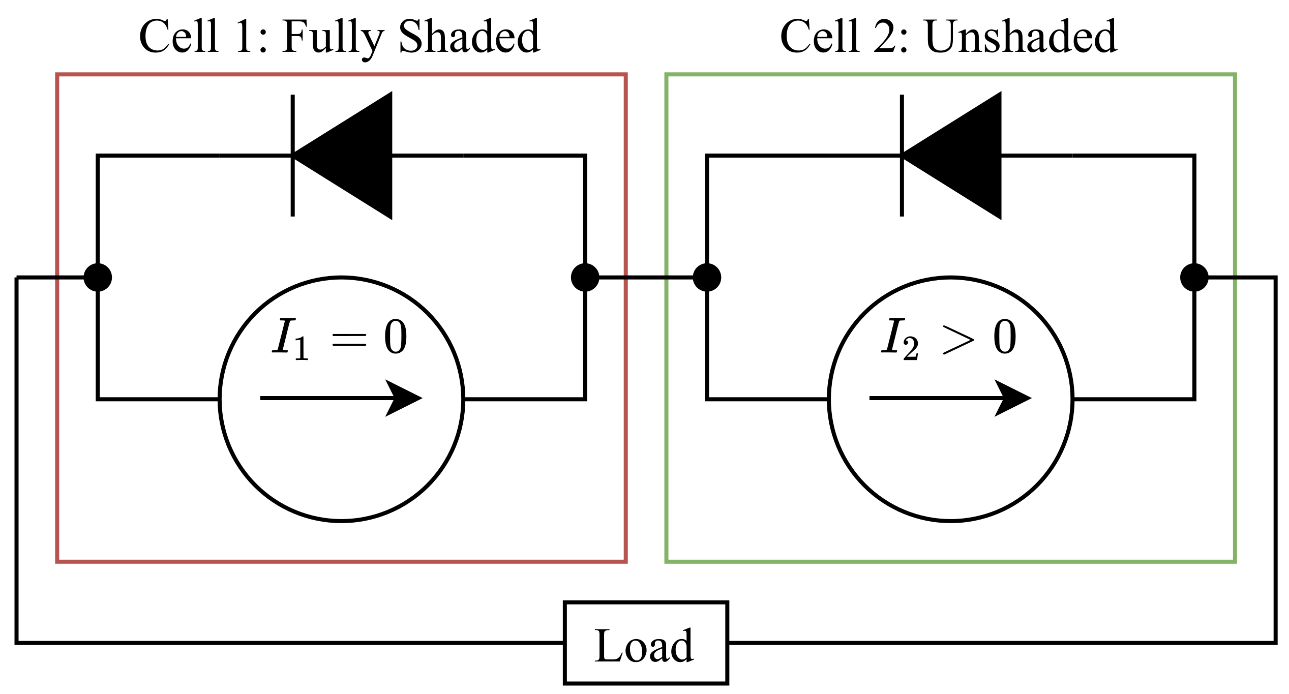
According to [1], the simplest equivalent model of a photovoltaic (PV) cell is composed of an ideal current source in parallel with a real diode. The current delivered by this current source is proportional to the solar irradiance falling upon the cell. As PV cells are not generally capable of producing large voltages on their own (a large cell may only produce [1]), multiple cells are commonly connected together in series to form a PV module. A large PV module, such as in [2], is often composed of 72 series-connected cells. When series-connected PV cells within a module receive differing levels of solar irradiance, this most simple model is no longer representative. Figure 1 (adapted from [1]) illustrates the conundrum—this model would suggest that no current could flow to the load if a single cell is shaded [1].
Figure 1.
Dilemma of two PV cells with differing solar irradiance represented by the simplest PV cell model.
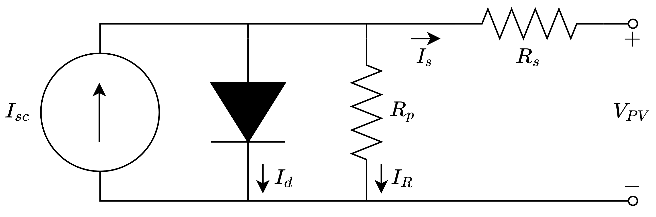
A parallel leakage resistance, , is often incorporated, which overcomes the aforementioned issue. Functionally, the component models the effects of leakage currents within the P-N junction [3]. Furthermore, a series resistance, , is commonly added to model the effects of contact resistances (such as those between the PV cell and its wire leads, as well as the resistances of the leads themselves) [1,3]. These additions result in what is frequently referred to as the single-diode model, which is shown in Figure 2 (adapted from [1]). Although the addition of now provides a current path through a completely shaded PV cell, the power dissipated in gives rise to the hot spot phenomenon, whereby the temperature of the PV cell increases. For a standard 156 × 156 (millimetre) PV cell, can be in the region of tens-to-hundreds of Ohms [4]. For a string current of multiple ampere, a fully shaded cell would dissipate an unsustainable level of power as heat energy. This is disadvantageous for two reasons: (1) electrical energy produced by unshaded PV cells in the string would be wasted, and (2) if the critical power dissipation (commonly denoted as ), a metric specified by PV cell manufacturers, is exceeded, then the shaded PV cell may become irreversibly damaged. In the case of the former, the power loss in a partially shaded PV installation is greater than the proportion of shaded area [5], and, in the case of a small PV installation, shading of a relatively small proportion of the plant may result in substantial power losses or the entire failure of the system [5,6]. From both the power production and cell longevity perspectives, it would be favourable to electrically remove shaded PV cells from a string, i.e., bypassing them [1,5,7,8].

Figure 2.
The single-diode model of a PV cell.
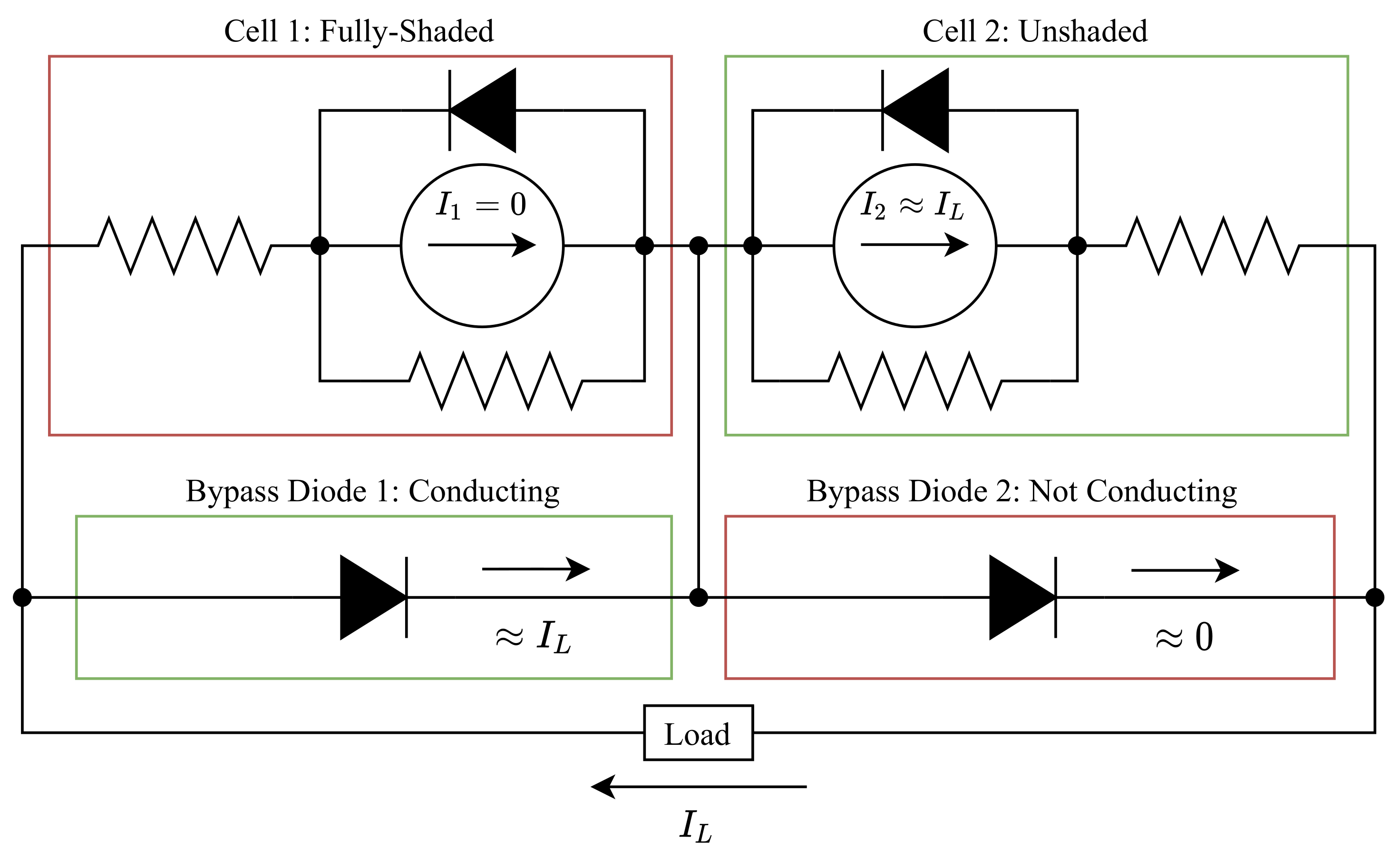
In order to accomplish this, a bypass diode is commonly added in parallel with either a single PV cell or a string of multiple series-connected PV cells. To illustrate the concept, a system of two series-connected PV cells is shown in Figure 3. Here, each PV cell is represented by the single-diode model, and these cells deliver current to a load. Each PV cell is also in parallel with a single bypass diode. During normal operation, with both PV cells exposed to equal levels of solar irradiance, both bypass diodes would be in reverse bias (i.e., only a negligible leakage current would be conducted through the bypass diodes). If, however, the PV cells were exposed to differing levels of solar irradiance, as is the case in Figure 3, then the bulk of the string current, , would pass through the bypass diode associated with the shaded PV cell. Little current may pass through the parallel leakage resistance of the shaded cell. However, the power dissipated in this cell would be greatly reduced (thereby mitigating the aforementioned negative effects of shading). Although it would be ideal for a bypass diode to be placed in parallel with each PV cell in a string, this is often cost-prohibitive and practically challenging. Hence, bypass diodes are generally placed in parallel with multiple series-connected PV cells, and are housed within a weatherised junction box on the rear of a PV module—as shown in Figure 4.
Figure 3.
Bypass diode operation in a PV system composed of two series-connected PV cells with differing solar irradiance.
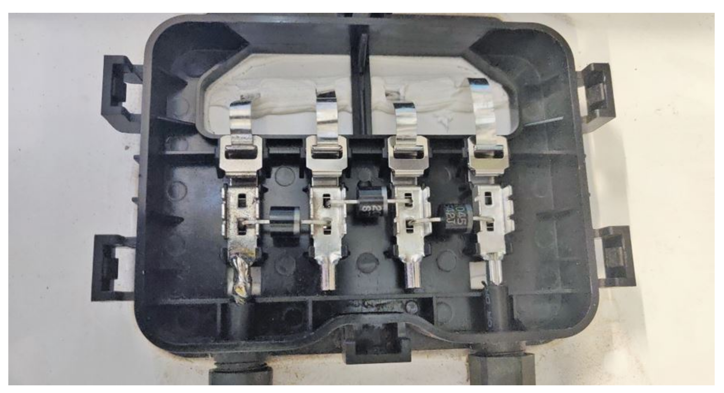
Figure 4.
The opened junction box of a BYD 310P6C-36 72 cell PV module, showing the connections of three bypass diodes.
When choosing an appropriate bypass diode, the forward voltage, , should be lower than the total breakdown voltage, , of the PV cell(s) across which the bypass diode is to be connected [8]. Furthermore, the maximum repetitive (peak) reverse voltage, , should be greater than the voltage produced by the PV cell(s) across which the diode is connected—thereby preventing reverse breakdown of the bypass diode during normal operation of the PV cell(s) [8]. Finally, the maximum average forward rectified current, , should be greater than the maximum PV string current [8].
Schottky diodes are the default choice for the bypass diode purpose. This is primarily due to their low forward voltages, which result in relatively low levels of dissipated power. Schottky diodes with a rated forward current of 10–20 , which typically have a forward voltage of 0.4–0.8 at this current, are generally suitable for this purpose [9,10,11].
The prevalent failure mode of a Schottky diode is a short circuit, which occurs when the diode is exposed to a large (typically transient) current in the reverse bias [12]. If this failure were to occur, the current produced by the PV cell(s) across which the bypass diode is connected would simply circulate through the short circuit—negating any possible contribution of those cells to the total string power.
Bypass diodes, therefore, play a critical role in the functioning of a PV system. Their correct operation is highly beneficial in terms of both power production and cell longevity. Their (short circuit) failure, especially if occurring early on and remaining undetected in a plant with a life cycle spanning multiple decades, would be tragic. Despite this, their operation is generally either over-simplified or omitted altogether in simulations and practical experiments involving the analysis of the effects of surges within PV systems [13,14,15,16].
As a result, it is imperative that the conditions to which bypass diodes are exposed within an actual PV system are well understood. This is most easily accomplished using computer simulation tools. For this, accurate models are required.
For completeness, it should be noted that much research has been performed on shade mitigation measures in recent years. At the array level, reconfigurable electrical interconnection strategies have been investigated. These strategies actively reconfigure the PV module interconnections, temporarily electrically removing entire PV modules, in order to attain maximum power production [17]. At the individual cell scale, [7] demonstrates a successful commercial implementation of miniature bypass diodes on a per-cell basis. Also indicated in [7] are multiple strategies for optimal bypass diode implementation, where each bypass diode protects multiple PV cells—either in an overlapping or non-overlapping manner. The authors of [18] reconsider the concept of bypass diodes altogether, indicating their long-term shortcomings and reviewing possible alternative measures for shading mitigation (including active switching-based techniques within PV modules).
Although great advances in shading mitigation techniques have been made, the simple Schottky diode-based mitigation strategy, whereby a single bypass diode is connected in parallel with a number of PV cells, is still prevalent in many PV installations. As PV plants commonly have an expected service life which extends beyond 20 years, it is not expected that this practice will change in short order. It is for this reason that accurate circuital modelling of the bypass diode operation at the traditionally implemented scale, for use in the simulation of surges within PV installations, will still be relevant for decades to come. In this article, three appropriate Schottky diodes are examined and modelled: the HY 10SQ045 [9], the DC Components Co. LTD. 15SQ040 [10], and the Vishay VSB2045 [11].
2. Proposed Circuital Model of Schottky Diode
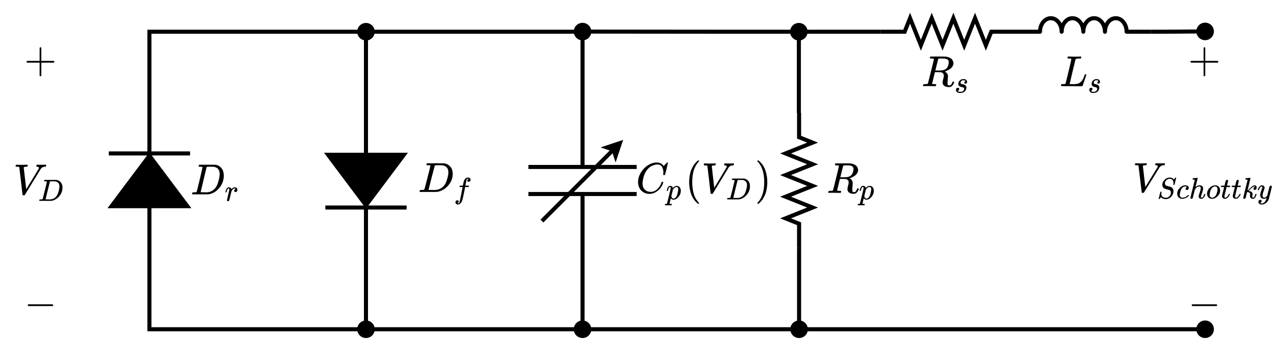
The proposed SPICE (Simulation Program with Integrated Circuit Emphasis) compatible full circuital model of a Schottky diode is shown in Figure 5. This model incorporates: a series inductance, , which models the inductive effects of the wire leads connected to the Schottky diode; a series resistance, , which models the contact resistances between the Schottky junction and the wire leads, as well as the resistance of the wire leads themselves; a parallel resistance, , which allows for the modelling of linear leakage currents within the diode; a nonlinear capacitance, , which models the effects of junction and diffusion capacitances within the diode; a forward-biased diode, , which models the nonlinear DC (direct current) forward bias characteristics of the diode, and a reverse-biased diode, , which models the nonlinear DC reverse bias characteristics of the diode. This circuital model is the combination of two sub-models: the DC large-signal sub-model and the alternating current (AC) small-signal sub-model.
Figure 5.
The proposed SPICE-compatible full circuital model of a Schottky diode.
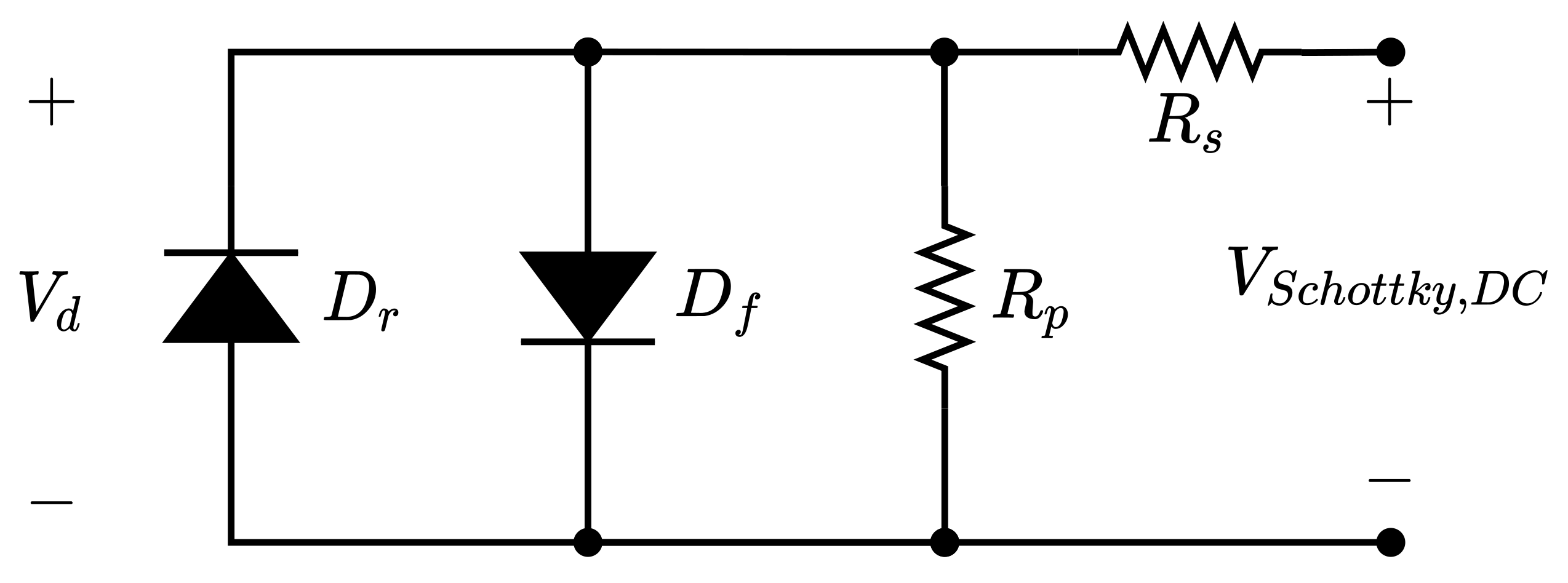
2.1. The DC Large-Signal Sub-Model
Under DC conditions, |, while |. Therefore, under these conditions, the parallel capacitor, , can be replaced with an open circuit, and the series inductance, , can be replaced by a short circuit. Substituting these revisions into the full circuital model produces the DC large-signal sub-model, which is shown in Figure 6.
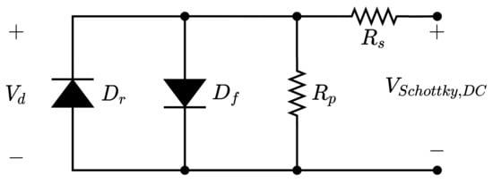
Figure 6.
The DC large-signal sub-model.
This two-diode approach was chosen due to the limitations of the default SPICE large-signal diode model, which is shown in Figure 7 (adapted from [19]). This model is composed of three circuital elements: an ohmic resistance , an internal diode , and a shunt conductance (which is present to assist convergence of the solver) [19].
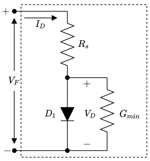
Figure 7.
The SPICE large-signal diode model circuit.
Figure 8 (adapted from [19]) shows the simulated current–voltage characteristics of this large-signal model. These characteristics are mathematically defined by Equations (1)–(4), where and represent the voltage over and the current through the diode, , respectively [19]. The thermal voltage, , is defined by Equation (5), where k is the Boltzmann constant and q is the charge on an electron—the values of these parameters are listed later in Section 4.1.1 [19,20]. The default values of the remaining parameters governing the operation of this model are listed, together with the corresponding parameter definitions, in Table 1 [19].
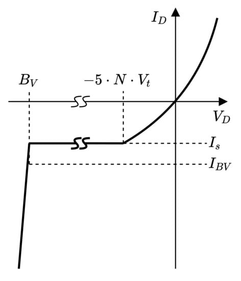
Figure 8.
The SPICE large-signal diode model current–voltage characteristics.

Table 1.
The SPICE large-signal diode model default parameters.
For :
For :
For BV:
For BV:
It is clear, as shown in Figure 8 and Equations (1)–(4), that the reverse-bias current–voltage characteristics of the SPICE large-signal diode model are greatly simplified, especially where . By incorporating a leakage resistance and a second diode, the DC large-signal sub-model enables further control over the simulated reverse bias behaviour of the modelled diode in the region before breakdown occurs—thereby overcoming the limitations of the SPICE large-signal diode model. It should also be noted that the built-in SPICE large-signal model does not include an inductance or a voltage-dependent capacitance—components required for accurate modelling under AC or transient conditions. The following sub-model, however, introduces these components.
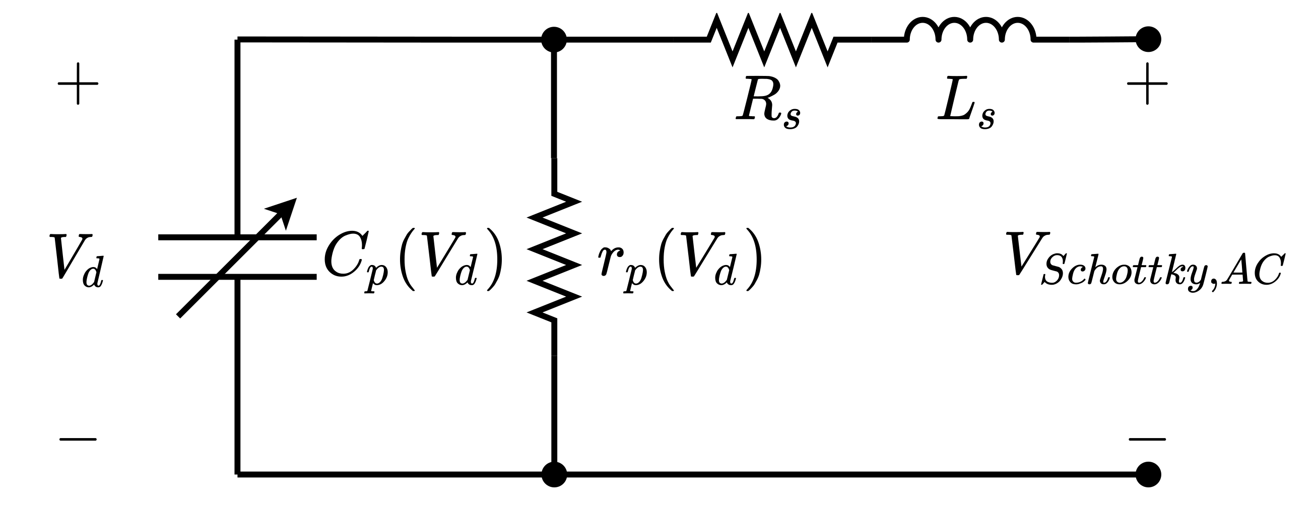
2.2. The AC Small-Signal Sub-Model
For a single DC operating point, the AC small-signal sub-model can be defined. This is shown in Figure 9. This circuital small-signal model is used in many publications, such as [4,21,22], for the purposes of diode modelling under AC conditions. This model is valid for small-signal AC diode modelling only, as large signal stimuli would result in a shifting of the operating point (and the resulting rectification effects). This model is, however, useful for extracting circuital parameters which are unlikely to change with environmental conditions, such as or . A resistance, , represents a linearised model of the parallel combination of the diodes ( and ) and the parallel leakage resistance () from the full circuital model at the specific operating point being considered. As a result, is a function of the DC voltage over these components, . The capacitance, , also varies with .
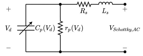
Figure 9.
The AC small-signal sub-model.
The equivalent impedance of the AC small-signal sub-model, denoted , is shown below in Equation (6).
where
and f is the frequency at that instant.
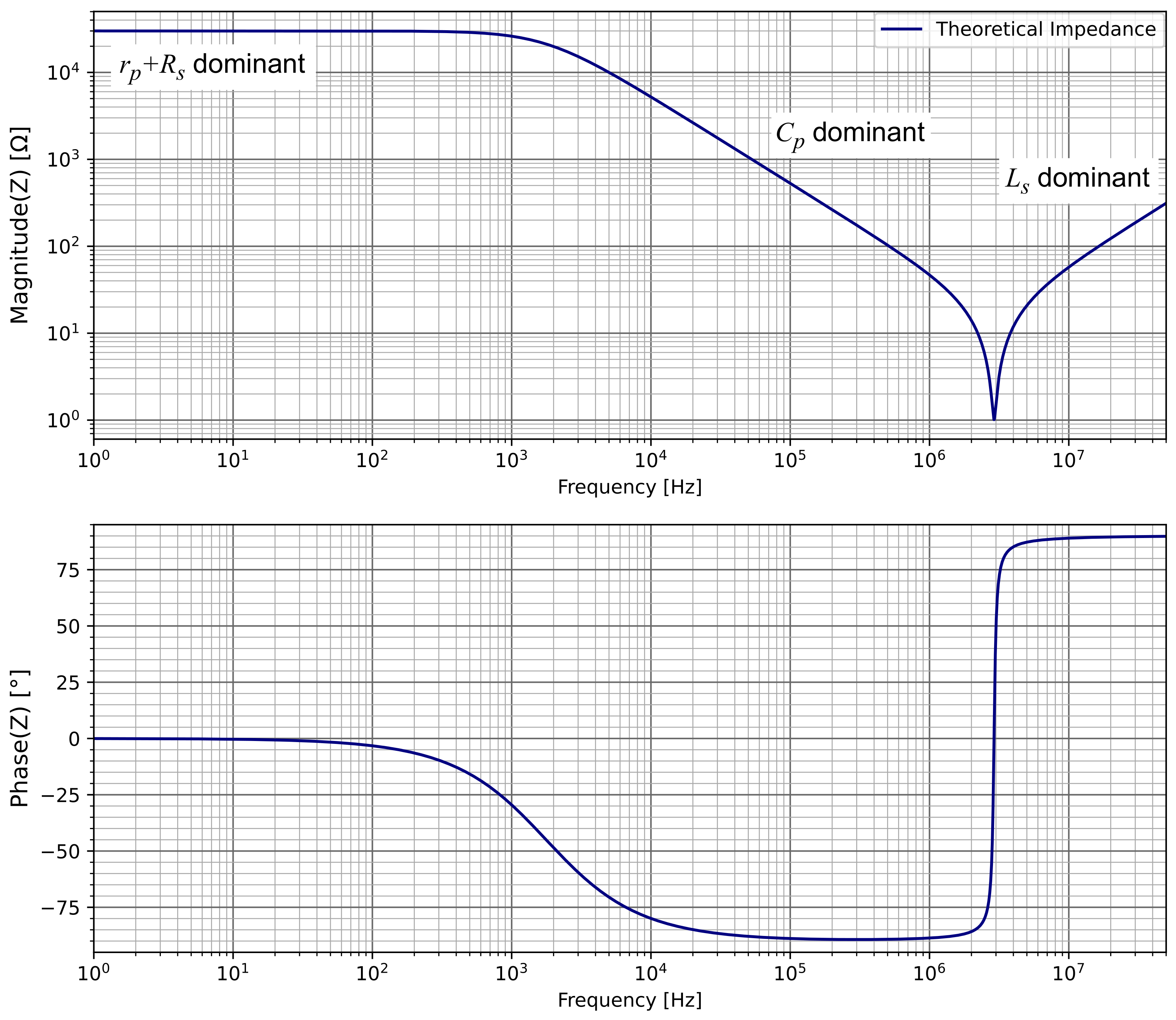
As an example, the equivalent impedance of the AC small-signal sub-model was calculated in Python [23] for frequencies between 100 and 50 , using the following component values: = 1 , = 3 , = 1 , = 30 . Magnitude and phase plots of this impedance were then generated using the Matplotlib Python library [24]; these are shown in Figure 10. As logarithmic vertical and horizontal axes are used for the magnitude plot, one can expect the magnitude plot to decrease linearly where the influence of dominates. Similarly, one can expect the magnitude to increase linearly where the influence of dominates. The influence of is dominant at low frequencies, where there is only a negligible change in impedance per change in frequency (, ). The series resistance, , is typically small, and therefore its influence is noticeably at the crossover between the dominance of and the dominance of . One can clearly observe this crossover point by examining the phase as it passes through 0° as it changes from approximately −90° to approximately +90° with increasing frequency.
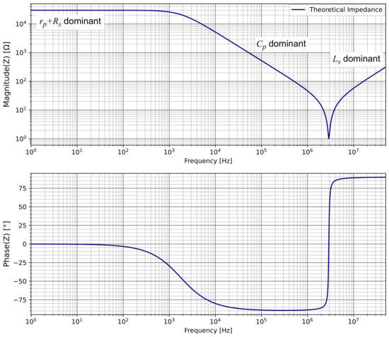
Figure 10.
Theoretical magnitude and phase plots for the Schottky diode AC small-signal sub-model.
It should be noted that, depending on the component values of the modelled system, as well as the bandwidth of the available measurement equipment, these regions of dominance may not always be clearly observable. In such a case, a curve fitting-based approach (using comparisons of the magnitude, the phase, or a combination) should be employed in order to obtain the parameters of the equivalent circuit from measurement. A prerequisite for this fitting procedure is that the measurement equipment employed must offer sufficient dynamic range. Therefore, the practical limitations of the measurement equipment need to be considered. These are covered later, in Section 3.
2.3. Voltage-Dependent Capacitance
In the region where the capacitance, , dominates the DUT (device under test) impedance, Z, the imaginary part of the impedance can be used to calculate the diode capacitance according to Equation (8). It should be noted that the negative term in the numerator will cancel out the negative term in the denominator, producing a positive capacitance, .
As the capacitance of a diode junction is a function of the width of the depletion region, which varies with voltage [25], it is necessary to sample the capacitance at multiple levels of DC bias. A curve may then be fit to these measurement, as in [26]. In order to ensure that the implemented voltage-dependent capacitance is suitable for simulations involving large-signal operation, a mathematical correction is first required prior to implementation in SPICE. This correction is described in the following subsection.
2.3.1. SPICE Modelling of a Voltage-Dependent Capacitance
After the necessary parameters are determined, the full circuital model of each diode can be implemented within SPICE. In this article, all SPICE circuit simulations were performed using LTspice [27]—a freeware SPICE-based simulator by Analog Devices. Components , , , , and are incorporated using standard SPICE components.
The implementation of capacitor is more complicated. A voltage-dependent capacitance can be defined in terms of either the total capacitance, , or the local capacitance, , which are calculated as shown in Equations (9) and (10), respectively [26]. Q represents the charge stored in the capacitor and v is the voltage over the capacitor [26]. The total capacitance is applicable to charge injection-based measurements, while the local capacitance is applicable to capacitances measured by means of a small-signal-based test at multiple DC bias voltages (as is the case in Section 4.4) [26].
Furthermore, the general template for a SPICE model of a voltage-dependent capacitor is defined by Equation (11), where i is the current through the capacitor [26]. This equation results from the differentiation of with respect to time (i.e., the application of the product rule of differentiation). The second term in Equation (11) can be ignored only when the resulting model is expected to handle small voltage perturbations [26].
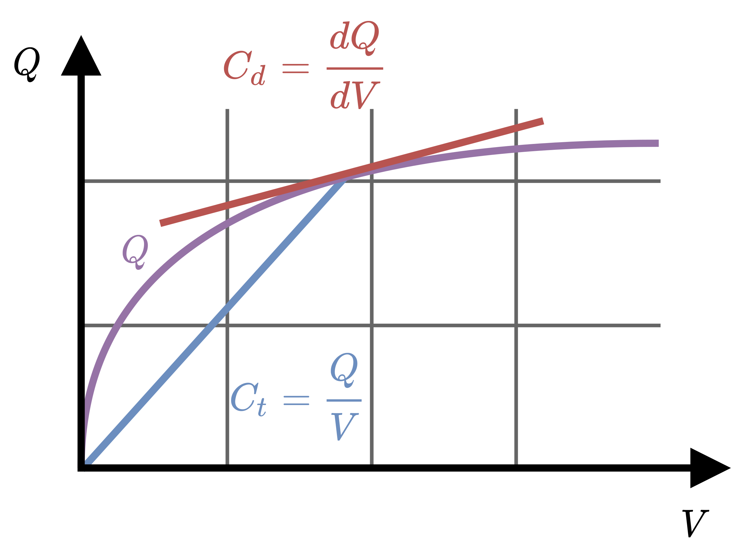
Figure 11 (adapted from [26]) illustrates the difference between and in relation to the total charge Q. For a linear capacitor, the relationship between the stored charge and the applied voltage would be a straight line; therefore, . For a nonlinear capacitor, .
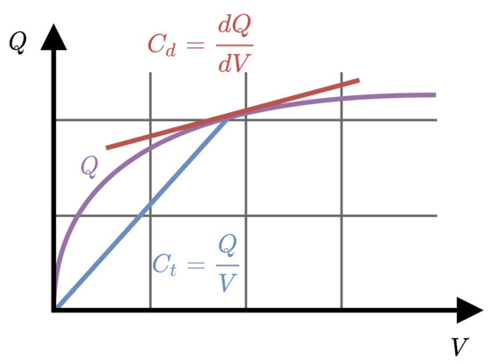
Figure 11.
An illustration of the difference between and .
A relationship between and can, however, be described as follows. Firstly, Equation (10) is rearranged to form Equation (12). Equation (12) is then integrated with respect to v, resulting in Equation (13). Equation (13) is then inserted into Equation (9) in order to form Equation (14), which allows for to be determined using and v [26]. This is useful as data gathered using small-signal measurements can be used to calculate the total capacitance, which would otherwise need to be measured by means of charge injection [26].
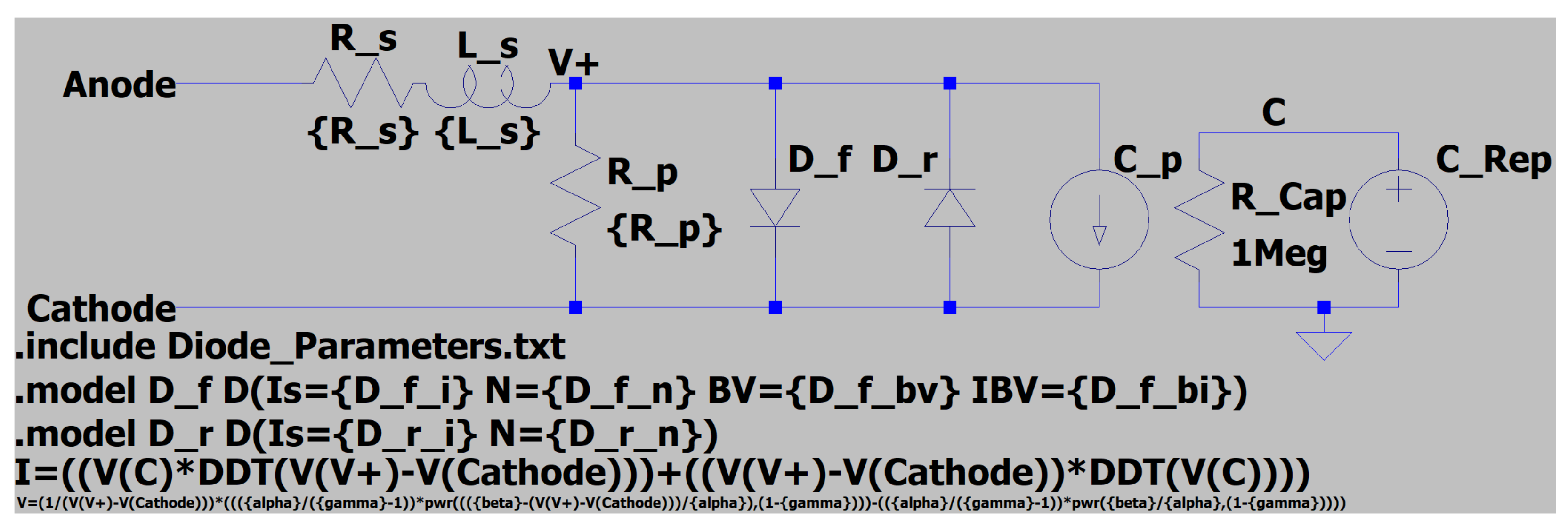
Applying Equation (14) to the fit voltage–capacitance curve, covered later in Section 4.4, allowed for the implementation of the voltage-dependent capacitance within LTspice [27]. This was accomplished using the behavioural current source-based technique from [26] and is shown as element C_p in Figure 12. This behavioural current source is controlled by Equation (11), using the DDT operator in LTspice to represent the terms. A behavioural voltage source, C_Rep, is used to calculate a voltage (the voltage at node C). The value of this voltage is equal to the value of the capacitance to be implemented by Equation (11). This value is calculated using the parameters and derived equation for presented later in Section 4.4. The voltage over element C_p is then defined as (V(V+)-V(Cathode)) in LTspice. As the voltage source C_Rep is only used to generate a voltage that represents the value of the capacitance, the resistance of R_Cap (chosen as 1 ) is irrelevant (as long as it is greater than 0).
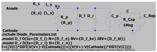
Figure 12.
The LTspice implementation of the full circuital model.
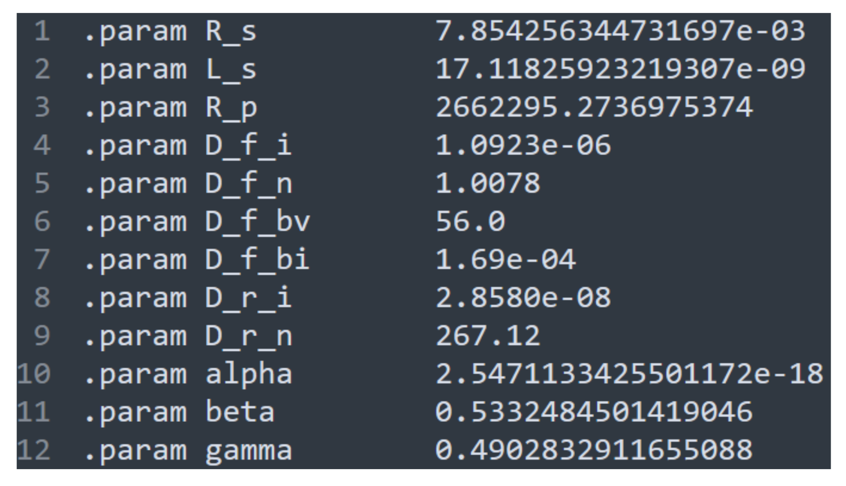
For simple editing, the model parameters can be included within a text file, as shown in Figure 13, and the full circuit can be implemented as a sub-circuit element, as shown in Figure 14.
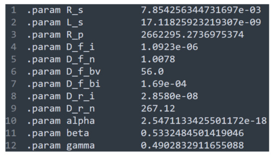
Figure 13.
The text file containing the parameters expected by the LTspice full circuital model. Parameters for the 10SQ045 diode are shown.

Figure 14.
A custom symbol representing the LTspice implementation of the full circuital model from Figure 12. A sub-circuit representation allows for easier use within large simulations.
A summary of the findings of this section is presented in the form of a tabular comparison of the suitability of the standard SPICE large-signal diode model, the commonly implemented AC small-signal model, and the proposed full circuital model, in Table 2 below.
Table 2.
A high-level summary of the suitability of the discussed models for different applications.
Now that the complete circuital model, as well as its LTspice implementation, have been described, the measurement setups employed will be discussed.
3. Experimental Tests
Two types of experimental test setups are used to examine the three different Schottky diodes. The first type of setup involves DC large-signal measurements, and the second type of test setup involves AC small-signal measurements. Two versions of the AC small-signal test setup are used—one which does not apply a DC bias voltage, and one which does. The strengths of each particular setup are exploited in order to obtain the most accurate results possible with the available equipment. All curve fitting in this article was performed using the curve_fit function from the SciPy Optimize open-source Python library [28], which employs a nonlinear least squares method.
3.1. DC Measurement Setup
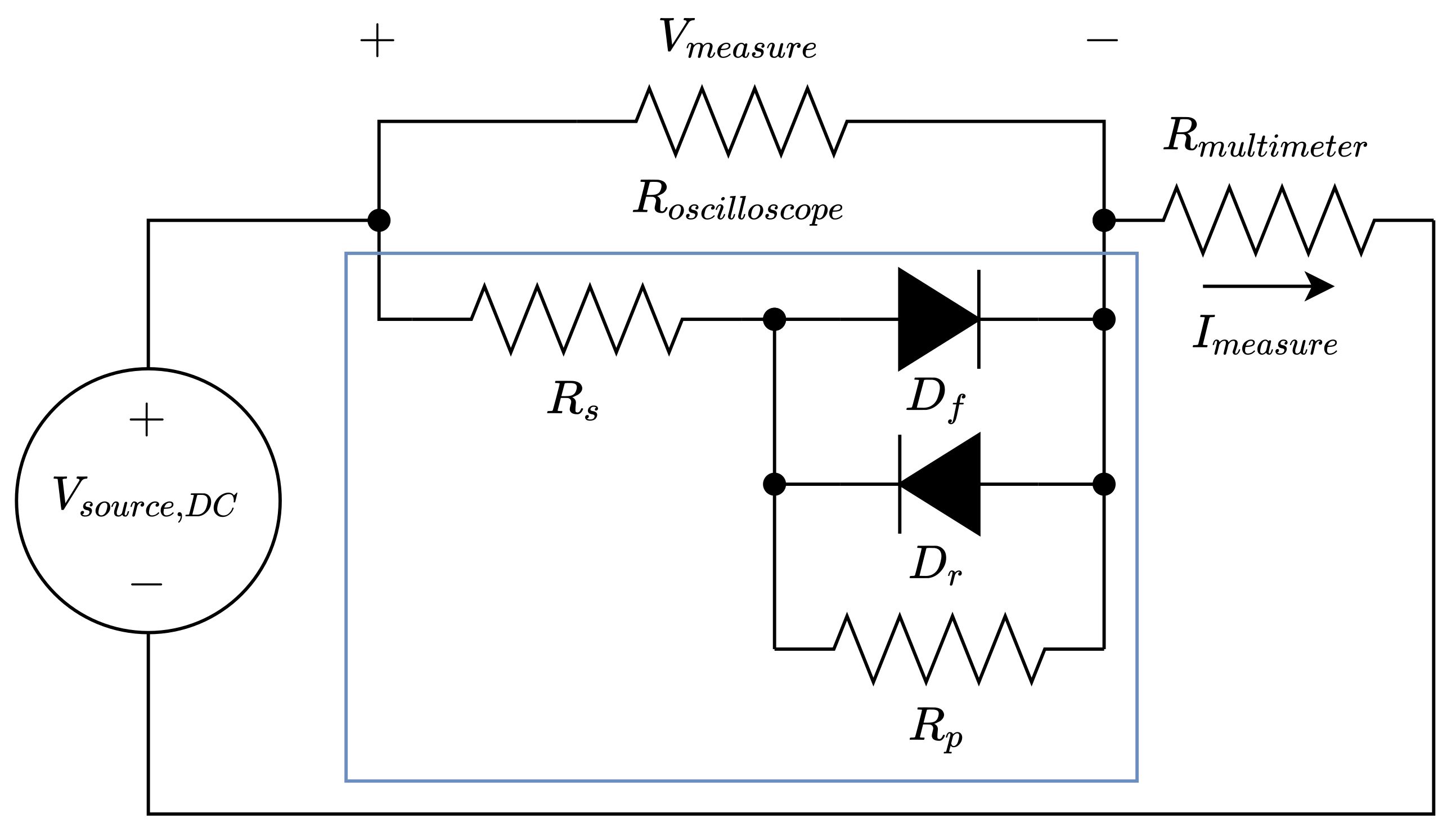
The DC measurement setup, shown in Figure 15, was the first setup to be used. It is composed of a DC voltage source, an oscilloscope, and a multimeter. The oscilloscope measures the voltage over the diode, and the multimeter measures the current provided by the DC voltage source. Instruments were chosen which offered sufficient accuracy for this purpose. The voltage of the DC source is swept over the desired range, and and are noted.
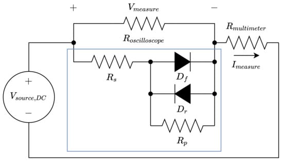
Figure 15.
DC measurement setup.
The voltage is positive when assessing the diode in forward bias, and negative when assessing the diode in reverse bias.
The input impedance of the oscilloscope, represented by , should always be considered. This is especially true when assessing the reverse-bias characteristics of the diode. As such, the influence of needs to be accounted for when analysing the measurement results. This is done by calculating the current flowing through the oscilloscope using Ohm’s Law (i.e., ), and subtracting this current from . was measured to be .
The remaining current is that which flows through the diode. The voltage was probed as close to the diode junction as possible, practically negating the component of , which was due to the resistance of the wire leads—this component is, however, measured later in Section 3.2.1.
This left only the component of , which was attributable to the resistance of the metal–semiconductor contacts, which was unobservable, and was therefore assumed negligible for this purpose.
The forward bias characteristics were examined first. In this bias, with the DC source connected as indicated in Figure 15, negligible current was assumed to flow through and . was adjusted such that the current through the diode was slowly varied between 0 and . Although greater current was available, the power dissipated by the diode would result in a noticeable increase in the junction temperature, affecting the thermal voltage, . This would cause the measured curve to diverge from the curve specified by Equation (1). This would be undesirable, as the SPICE diode model assumes a constant operating temperature. The input impedance of the oscilloscope was compensated for, and Equation (1) was fit to the measured results.
The reverse bias characteristics were then examined. was started at 0 and increased until just after the breakdown of each diode junction was observed. The influence of the input resistance of the oscilloscope was then accounted for. The influence of the leakage current through , which had a value of − according to Figure 8, was also compensated for. The reverse bias current–voltage characteristics were then analysed between 0 and 25 —below the breakdown voltage of the real diodes. In this voltage range, the bulk of the reverse current flowed through , and this exhibited a linear trend. The gradient of this linear trend allowed for the calculation of .
Once the current through was accounted for, the only remaining current was that through . The remaining current–voltage curve was then fit to Equation (1) in order to determine the nonlinear reverse bias diode parameters, which would dominate in the reverse bias voltage range between −5NVt and .
These forward and reverse bias current–voltage sweeps were sufficient to extract parameters, presented in Section 4, which enabled accurate modelling of the DC operation of the diodes. Next, the dynamic behaviour of the diodes was considered.
3.2. AC Small-Signal Measurements
Small-signal impedance measurements of each diode were performed using an OMICRON Lab Bode 100—a low-frequency VNA (vector network analyser) [29]. The resulting measurements allowed for the extraction of the remaining parameters (, , ) for each of the three diodes. Firstly, parameters which would not change with different operating points (i.e., and ) were extracted from measurements involving no DC bias. Then, the capacitance, , of the diodes was measured for multiple levels of DC bias (as it was bound to change with different levels of reverse bias).
3.2.1. Without DC Bias
The magnitudes of and do not noticeably change with DC bias. Furthermore, was likely to be very small; therefore, a sensitive measurement was necessary. An OMICRON Lab B-WIC impedance test fixture, shown in Figure 16, was used with the Bode 100 in order to measure the impedance of the three diodes (without a DC bias applied). This fixture, designed for impedance measurements of THT (through-hole technology) components, allowed for the impedances of the diodes to be assessed while being in a similar arrangement as they would be in the junction box of a PV module. The fixture has a bandwidth of 1 to 50 [30]. When employing a receiver bandwidth of 10 , the measurement accuracy is stated as 2% for impedances down to (up to 2 ), and 10% for impedances down to 20 (up to 300 ) [30]. Above these specified frequencies, the 2% and 10% accuracy limitations are governed by inductances of and 10 , respectively [30].
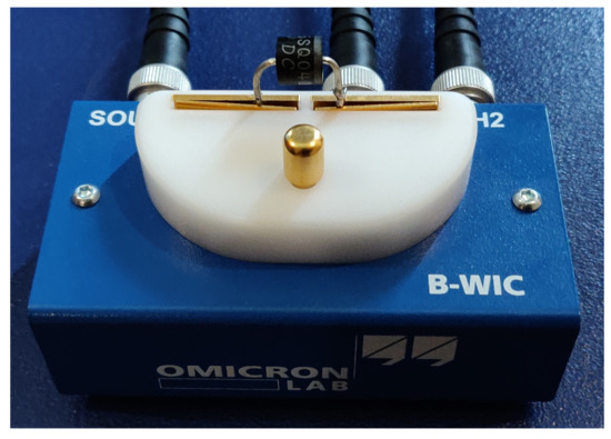
Figure 16.
The OMICRON Lab B-WIC impedance adapter for THT components.
The gold-plated electrodes used by this fixture have a contact resistance of approximately [30]. The magnitude of was chosen as the lowest value of the real impedance measured for each diode. The magnitude of was calculated using the value of the imaginary impedance of each diode at 50 and . As and do not change with DC bias, the signal level of the Bode 100 could be set as high as 13 . This is because these parameters would remain constant even if the nonlinear behaviour of the diodes were to be excited. This allowed for a better signal to noise ratio, resulting in a more accurate measurement.
3.2.2. With DC Bias
The magnitude of the capacitance of a Schottky diode changes with the magnitude of the DC reverse bias voltage applied to the diode. This is, as previously mentioned, due to a change in the width of the depletion region [25,31]. The measurement circuit shown in Figure 17 was required in order to measure the capacitance of each diode at multiple DC bias points. This measurement circuit is composed of two parts, the Measurement Bridge and the DC Bias Tee. The purpose of the measurement bridge circuit is twofold. Firstly, it extends the measurement range of the Bode 100 to several hundred [32]. Secondly, it provides protection to the output and input terminals on the Bode 100 by means of voltage division. The absolute maximum ratings of the output and input terminals are RMS and 7 RMS (or 50 DC), respectively [29]. The DC Bias Tee allows for the biasing of the DUT (device under test) (which is represented by the impedance in Figure 17) while further protecting the output terminal on the Bode 100 from the DC voltage. The DUT is in parallel with the series combination of resistor and the DC source. Choosing a large value for ensured that the impedance of the series combination of the DC source output impedance and was far greater than the impedance of the DUT. Consequently, the influence of the impedance of the DC source on the measurement would be negligible. The component values used in the full measurement setup are listed in Table 3, and a photograph of the inner circuitry is shown in Figure 18. The aluminium lid was replaced before measurements were conducted, and the DIP (dual in-line package) switches allowed for an appropriate resistor to be selected.
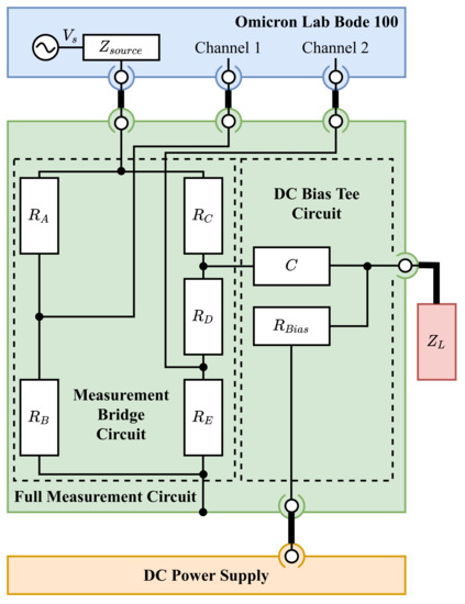
Figure 17.
Block diagram of the measurement setup for DC-biased AC small-signal analysis.
Table 3.
Component values for the full measurement setup.
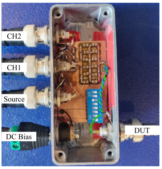
Figure 18.
The constructed measurement circuit.
A common trade-off when examining nonlinear devices is the dichotomy between the signal-to-noise ratio and the linearity of the test setup. A high signal-to-noise ratio produces a result that is stable and uncorrupted by noise. Increasing the source level is one way of improving the signal-to-noise ratio. If, however, the source level is increased too much, then the nonlinear operation of the DUT may influence the result, i.e., the operating point changes, and more than only the small-signal operation is measured. For this reason, a correct signal level at the DUT connection is key.
4. Results
Results were gathered for both the DC large-signal and AC small-signal cases.
4.1. DC Results
For the DC current–voltage measurements, the voltage probe was placed as close as physically possible to the diode junctions. This was in order to negate the influence of the resistance of the wire leads on , leaving only the resistive influence of the contact between the junction and the wire leads. This remaining component of was then observed to be negligible for these measurements (i.e., no discernible linear trend that was attributable to was embedded within the measured data).
4.1.1. Forward Bias
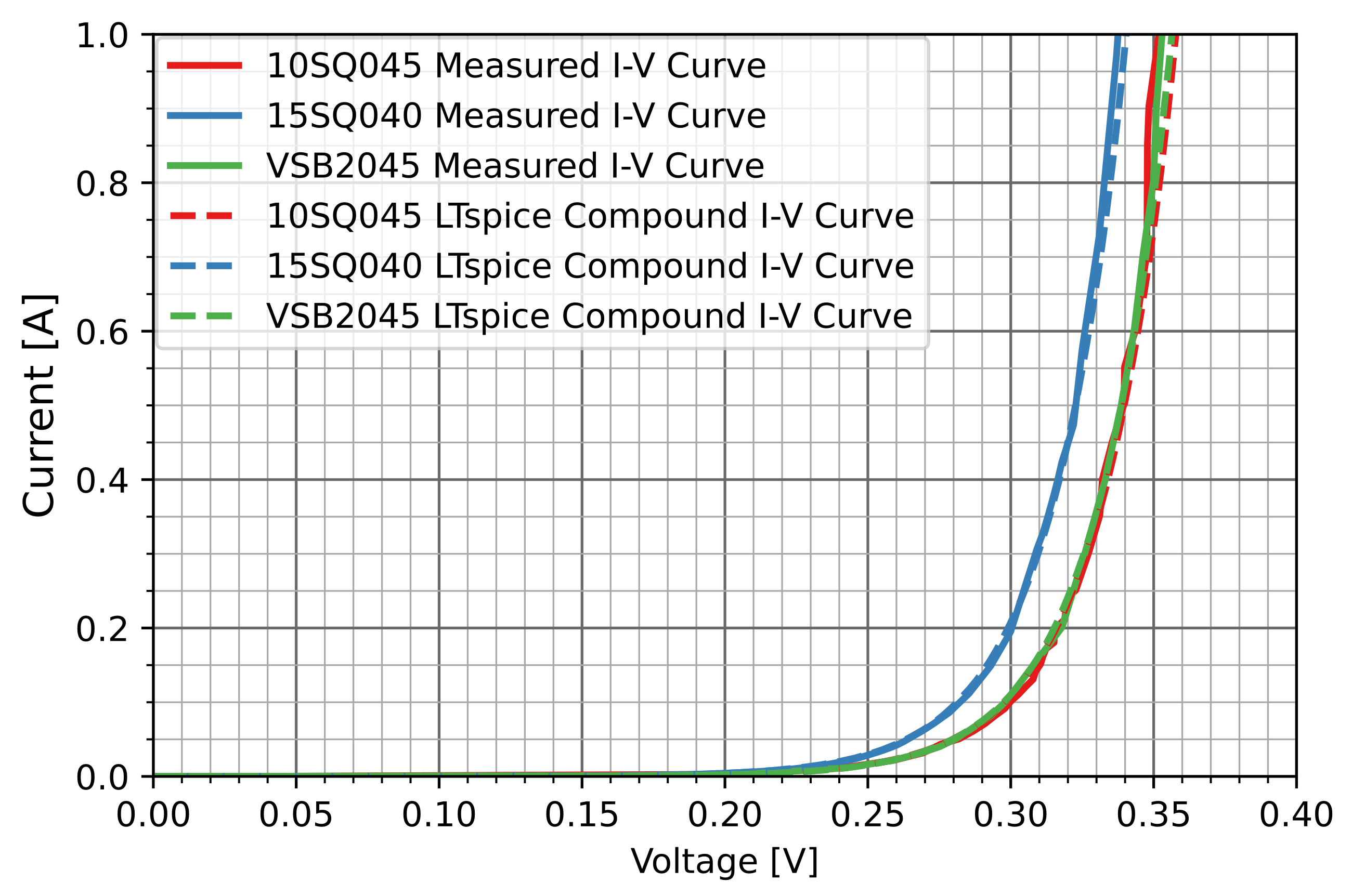
The forward bias case was considered first. Although the influence of the oscilloscope input resistance would be negligible for the forward bias measurements, its influence was compensated for nonetheless. Nonlinear curve fitting was performed for the three diodes using the Shockley equation as the objective function, i.e., Equation (1), with the convergence-assisting parameter, , set to 0. The thermal voltage, , was calculated with Equation (5) using the parameters listed in Table 4. The default values for k (the Boltzmann constant) and q (the charge on an electron) were used [20]. Due to the difficulty in measuring the junction temperature of the diode (as a result of the plastic casing), T was assumed to be the same as the ambient temperature for the low power levels tested. This fitting procedure produced the parameters which are listed in Table 5. The resulting measured and fit current–voltage curves for the three diodes are shown in Figure 19. Good agreement was achieved for all three diodes for the forward bias. Divergence from the modelled trends begins to occur at larger currents—this is attributed to the influence of a decreasing thermal voltage, , as the result of an increasing junction temperature, T, as the power dissipated in diode junctions increases.
Table 4.
Forward bias curve fitting parameters for the three diodes.
Table 5.
Forward bias () curve fitting parameters for the three diodes.
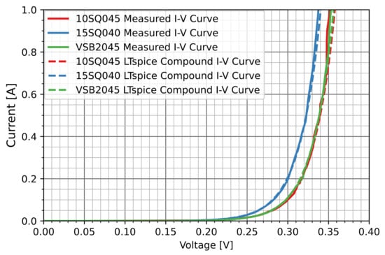
Figure 19.
Nonlinear fit of for large positive DC voltages for the three diodes.
4.1.2. Reverse Bias
The reverse bias case was then considered. The reverse voltage over each diode was increased until just after breakdown occurred. Breakdown was regarded as the sharp point where the reverse current began to increase rapidly for even a minor increase in the reverse voltage; this is illustrated in the measured results later in this section. The reverse breakdown voltages, as well as the corresponding reverse currents, are listed in Table 6 below.
Table 6.
Reverse breakdown voltages and currents for the three diodes.
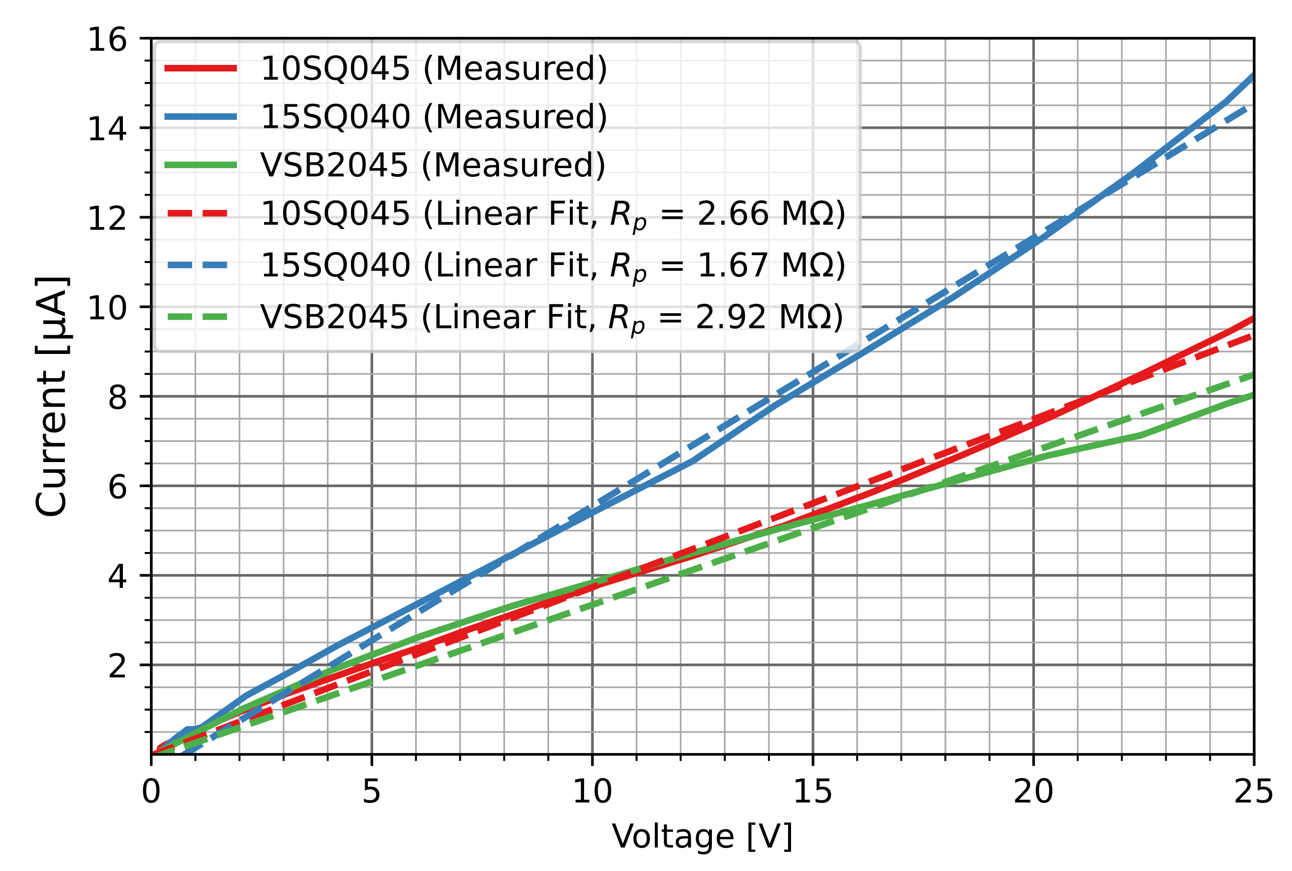
The parallel leakage resistance, , has the greatest influence at low voltages—well before the effects of reverse breakdown are noted. After compensating for the input impedance of the oscilloscope, as well as the influence of the from the forward bias case (due to the leakage through as a result of the SPICE diode model), a linear curve was fit to the measured data for the region between 0 and 25 . This allowed for to be calculated for each of the three diodes. The resulting values of are listed below in Table 7, and the measured and fit current–voltage plots are shown in Figure 20.
Table 7.
for the three diodes.

Figure 20.
Linear fit of for small negative DC voltages for the three diodes.
After was calculated, its influence was removed from the measured data. This left only the current–voltage relationship of , to which the Shockley equation was fit for the region between 0 and the lowest voltage above which reverse breakdown of the diodes would occur. The parameters for the resulting fit are listed in Table 8. The measured and fit current–voltage curves for the component of the three diodes are shown in Figure 21.
Table 8.
Reverse bias () curve fitting parameters for the three diodes.
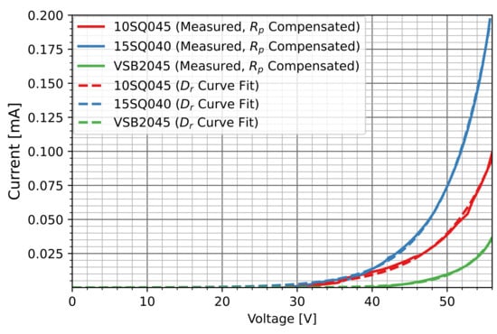
Figure 21.
Nonlinear fit of for large negative DC voltages for the three diodes.
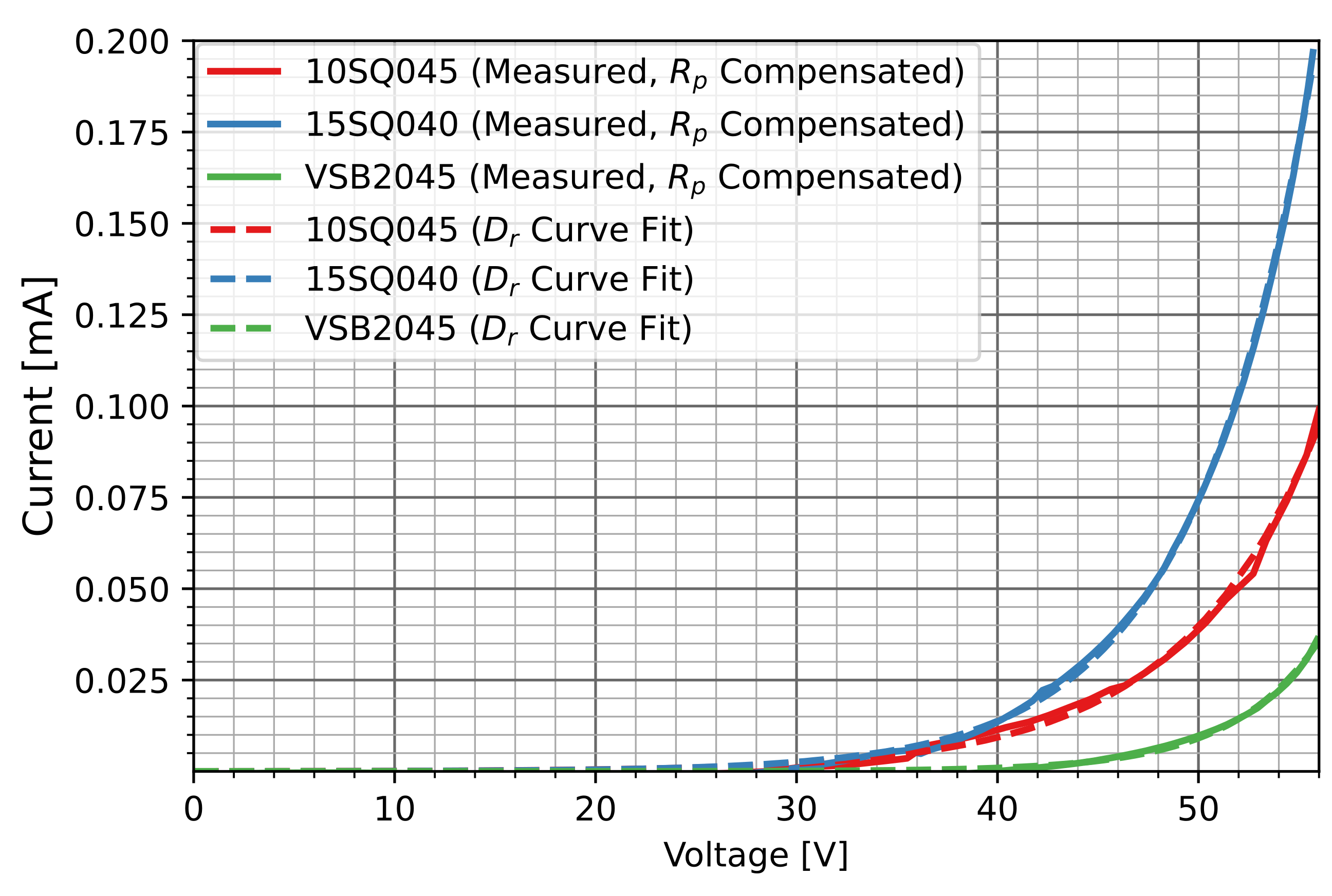
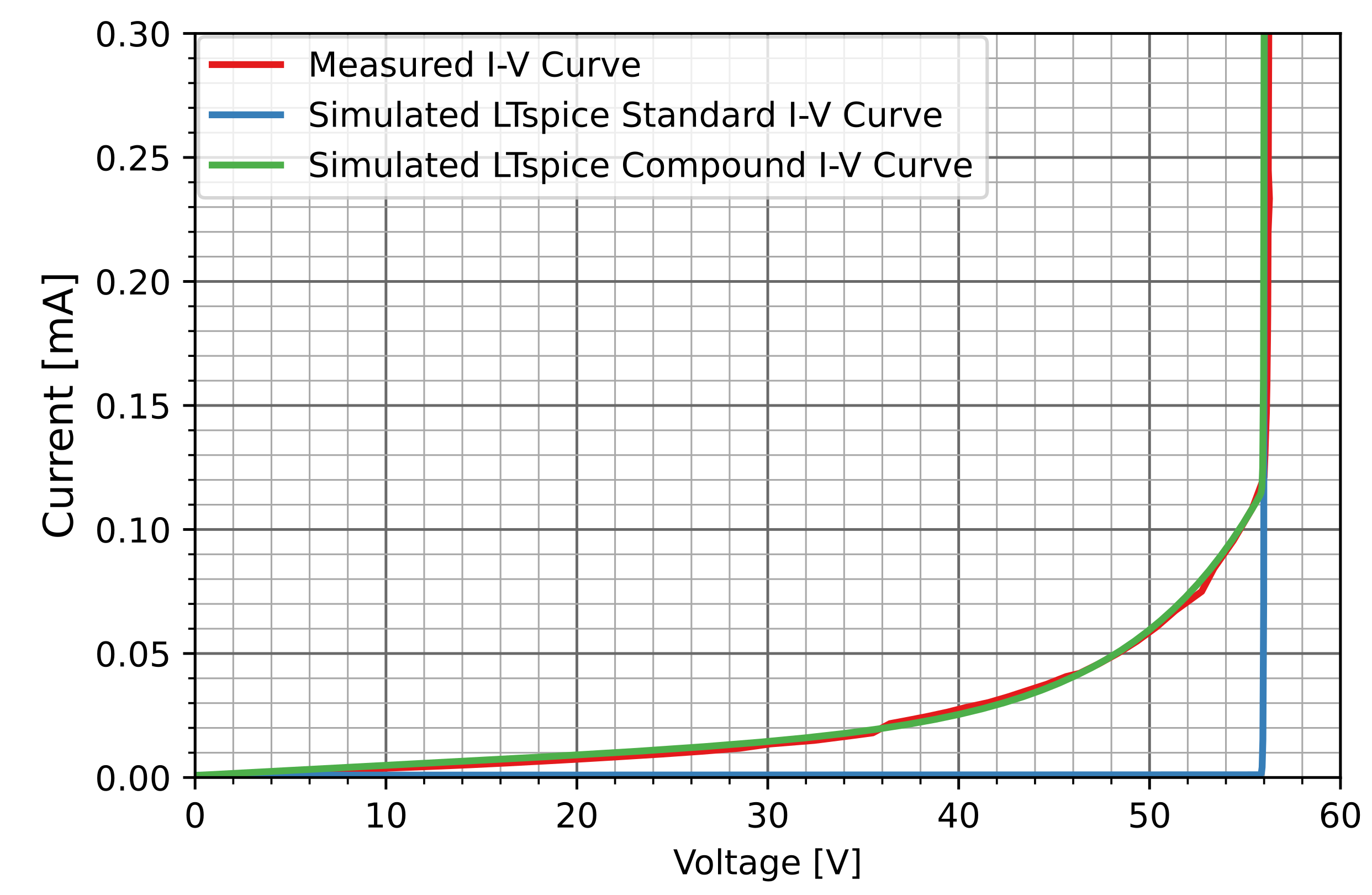
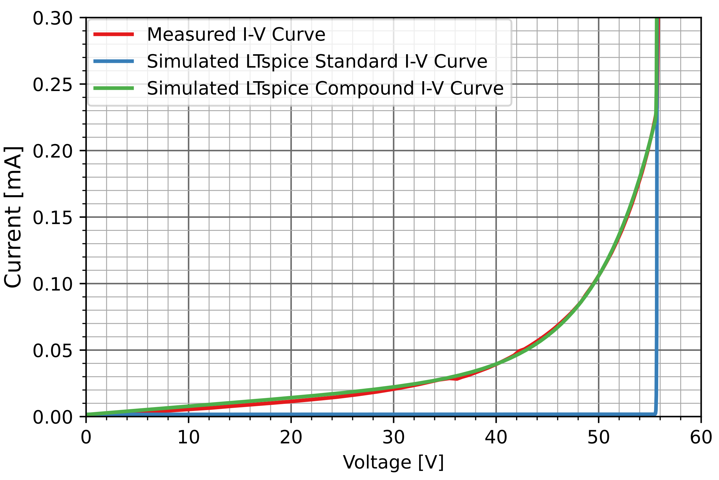
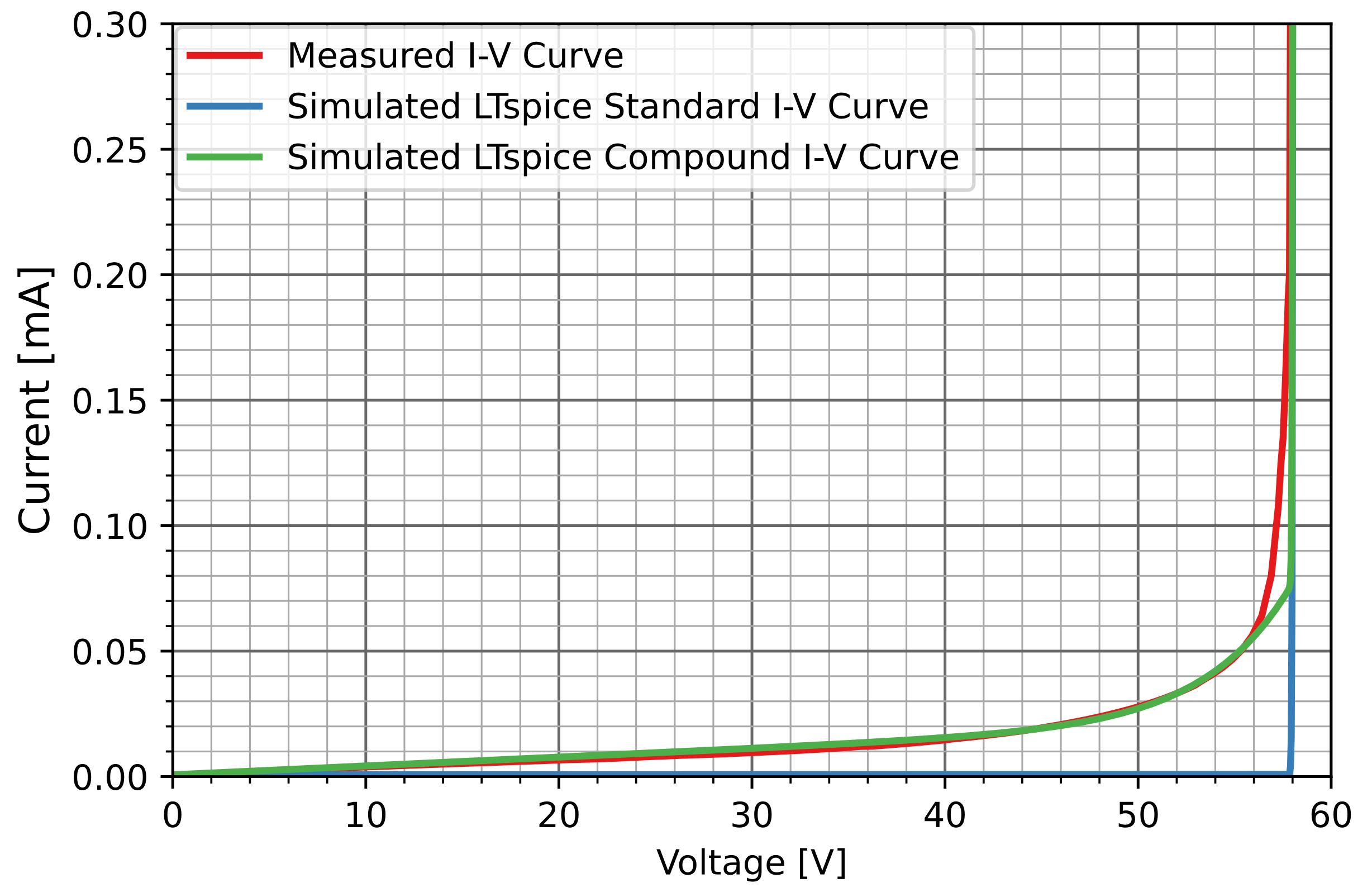
Finally, the breakdown voltage and current of each diode were entered into the component of the DC large-signal sub-model, along with the parameters from Table 5, Table 7 and Table 8. With set to 0 in each case, the DC large-signal sub-model for each diode was simulated in LTspice. Simulations were also performed with and removed from the model, in order to illustrate the difference between the proposed DC large-signal sub-model and the standard SPICE current–voltage reverse breakdown behaviour. The results for the 10SQ045, 15SQ045, and VSB2045 diodes are shown in Figure 22, Figure 23 and Figure 24, respectively. For the 10SQ045 and 15SQ045 diodes, the DC large-signal sub-model accurately models the measured reverse bias current–voltage relationship. The VSB2045 model is also accurate, except for a minor disagreement between the reverse voltages of 56 and 58 . In general, the reverse bias current–voltage characteristics of the DC large-signal sub-model far exceed the accuracy of the standard SPICE large-signal model.
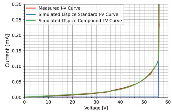
Figure 22.
Measured and simulated reverse bias plots for the 10SQ045 diode.
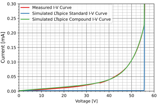
Figure 23.
Measured and simulated reverse bias plots for the 15SQ040 diode.
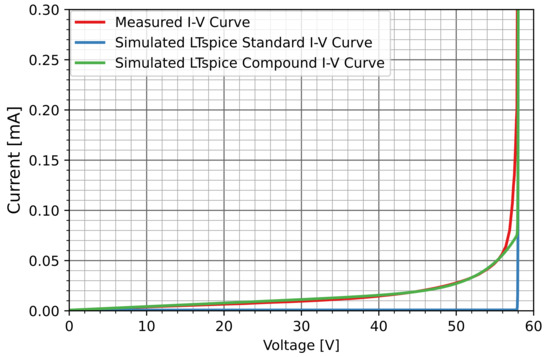
Figure 24.
Measured and simulated reverse bias plots for the VSB2045 diode.
4.2. AC Small-Signal Results
AC small-signal results were then gathered, firstly without and then with the application of a DC bias voltage, in order to determine , , and .
4.3. Unbiased AC Small-Signal Results
The diodes were positioned within the THT measurement fixture such that the length of the wire leads was representative of the lengths that would be necessary when implemented within the junction box of a PV module. This was critical for accurate modelling, as, if the leads were shortened, then the effect of the series resistance, , and inductance, , that is due to the wire leads would have been omitted.
Initially, a frequency range of 1 to 50 was chosen, with 401 logarithmically spaced measurement points. The attenuation of both receivers was set to 0, and the receiver bandwidth was set to 10 . This configuration achieved good measurement accuracy (i.e., an appropriate signal-to-noise ratio) and sweep time. An Open-Short-Load calibration was performed using the calibration kit provided with the B-WIC fixture. This allowed the parasitic elements of the measurement setup to be compensated for. This initial sweep allowed for the resonant points of each diode to be identified. The measurement range was then adjusted to 1 to 50 , again with 401 logarithmically spaced measurement points, as this allowed the regions before and after the resonant point to be examined with greater resolution. As the resonant point identified for each diode occurred between 10 and 30 , further measurements were conducted within this frequency range in order to more accurately determine the value of for each diode. For these further measurements, the Bode 100 was recalibrated, this time using 401 linearly spaced points. Using the curve_fit function, with the magnitude of Equation (6) (the impedance equation for the AC small-signal sub-model) as the objective function, parameters for and were obtained. In this curve fitting procedure, the values from Table 7 were used for parameter . As this small-signal measurement was conducted without a DC bias, the assumption that (from Section 4.1) was made.
The term (from Equation (6)) was calculated for each diode at its corresponding resonant point, and these values were then subtracted from the corresponding measured real impedance values. This produced the measured values for parameter for each diode. The gold contact resistance of , mentioned earlier, was also subtracted in order to correct the measured values of for each diode. The aforementioned parameters are listed in Table 9.
Table 9.
AC small-signal parameters for the three diodes.
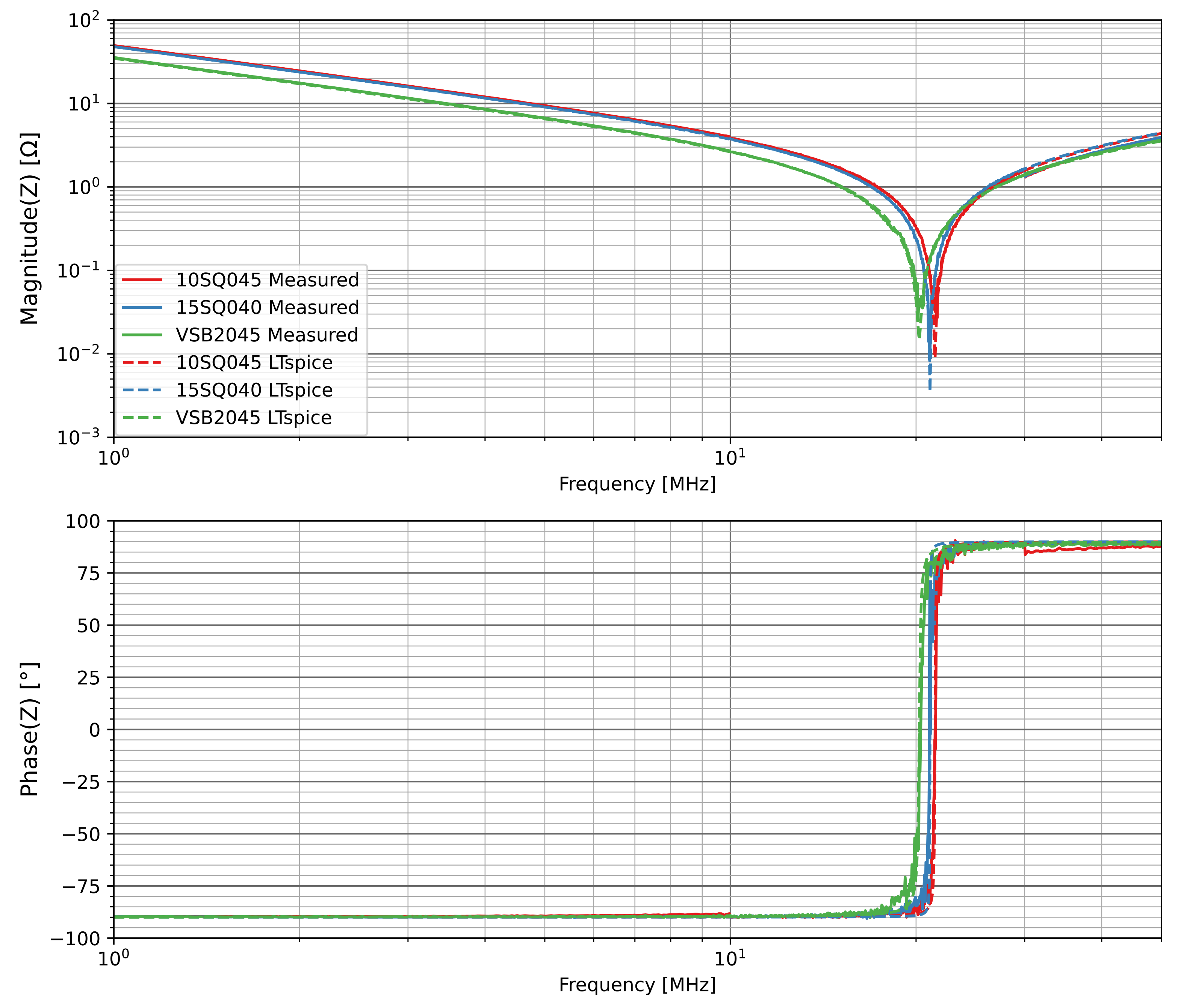
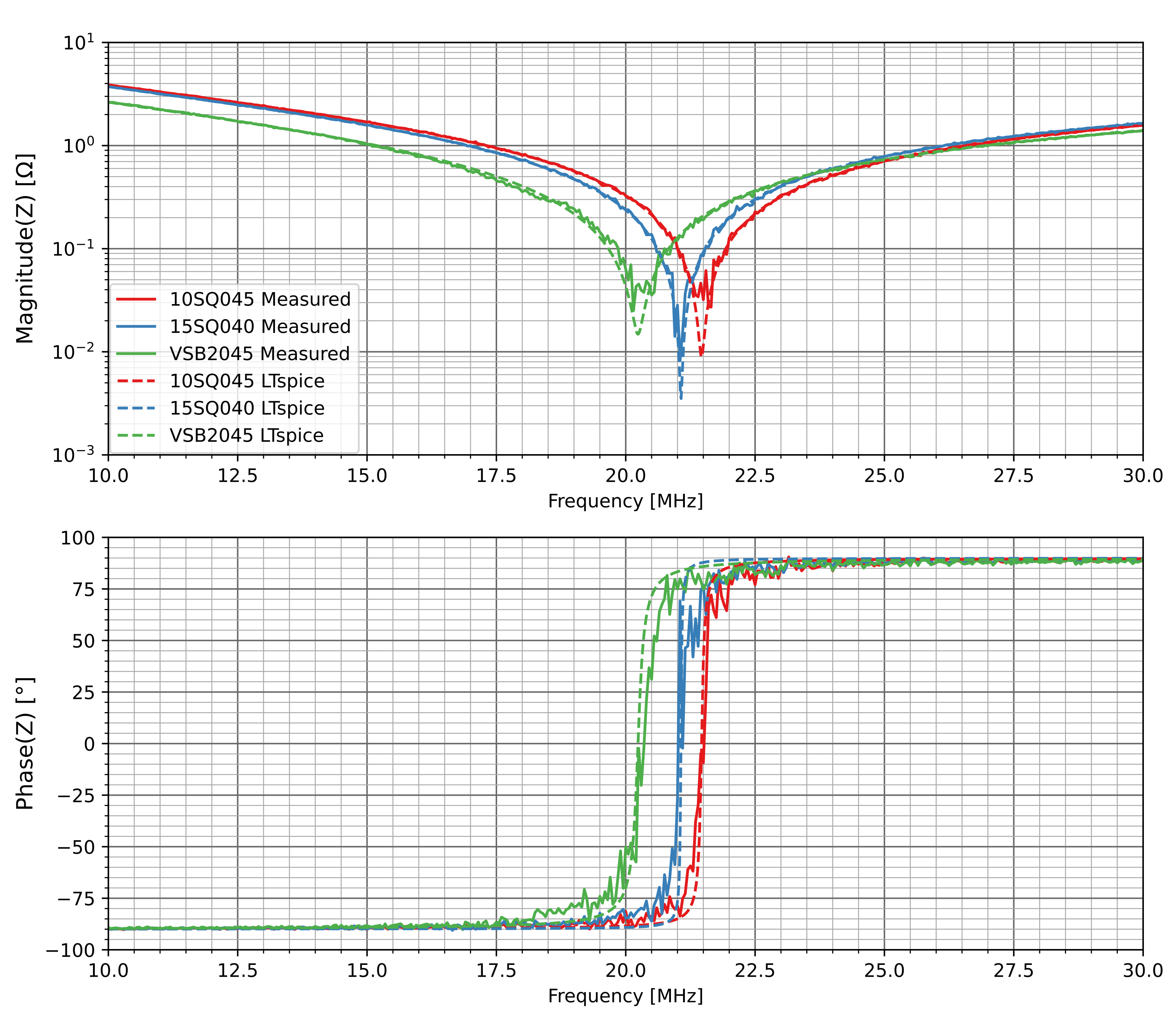
LTspice simulations were performed for each diode using the AC small-signal sub-model, with the parameters from Table 9. Figure 25 demonstrates good agreement, in both magnitude and phase, of the measured and simulated impedances using a logarithmically spaced frequency axis between 1 and 50 . Figure 26 further exhibits this agreement in more detail about the resonant point using a linear frequency axis between 10 and 30 .

Figure 25.
Measured and simulated magnitude and phase plots of the three diodes between 1 and 50.
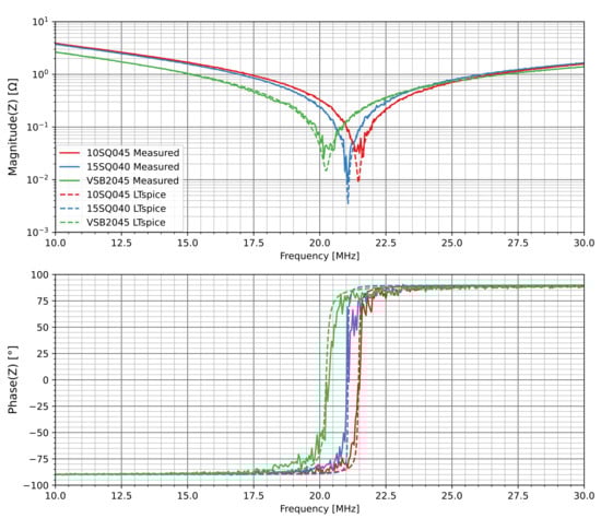
Figure 26.
Measured and simulated magnitude and phase plots of the three diodes between 10 and 30.
These plots clearly demonstrate the resonant point between and the parallel combination of and . dominates below this frequency, and dominates above this frequency. It should be noted that the curve fitting procedure was crucial in order to obtain accurate values for , as no region where the magnitude of the impedance of the diodes was exclusively influenced by the inductance was present. For this, a frequency higher than 50 would have been required—outside of the capabilities of the Bode 100.
Now that the parameters for , , , , and had been determined, the only remaining unknown parameter was the voltage-dependent capacitance, .
4.4. Biased Measurements—Capacitance Measurement
The impedance of each diode was measured at 401 logarithmically spaced points between 100 and 50 , for reverse bias voltages between 0 and 35 (in 1 increments).
According to the diode datasheets, the junction capacitances of the three diodes were all sampled at 1 , at a DC reverse bias voltage of , by their respective manufacturers [9,10,11]. For a valid comparison, the diode impedances were sampled at the closest frequency within the measured range ( ). At this frequency, the accuracy of the measurement setup was confirmed using a range of known capacitances. Due to the expected impedances spanning several orders of magnitude, and the relatively limited dynamic range of the measurement setup, this single-point approach was more appropriate than employing a curve fitting procedure spanning the full measurement range.
Following the power-to-voltage calculations in Appendix A, the source level was set to a constant . This was theoretically low enough so as not to cause the diodes to exhibit nonlinear operation. However, this fact was also confirmed using oscilloscope measurements at the DUT. The attenuation of both receivers was set to 0, and the receiver bandwidth was set to 30 . This configuration achieved a good balance between measurement accuracy (i.e., an appropriate signal-to-noise ratio) and sweep time.
An Open-Short-Load calibration, using the calibration kit provided with the Bode 100, allowed for the topology and parasitic elements of the measurement setup to be considered and compensated for, respectively. In order to further decrease the effects of measurement noise, the measured results were then passed through a convolution-based digital filter. The Savitsky–Golay filter (from the SciPy open-source Python library [28]), with a window size of 51 and a polynomial order of 2, was then applied in order to adequately smooth the measured data without distortion of the signal tendency.
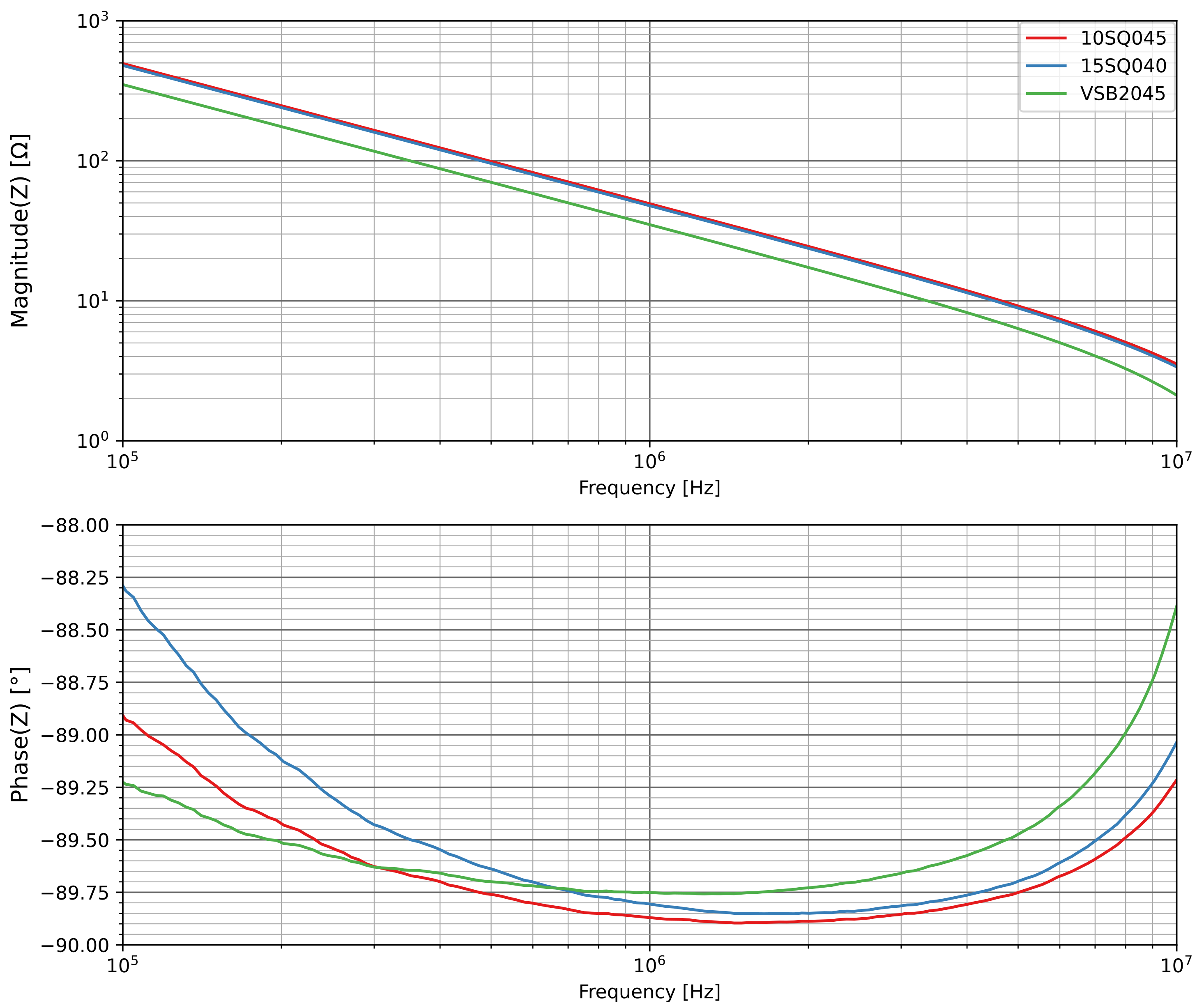
Between 100 and 10 , the magnitude of the measured impedances decreased linearly with increasing frequency, while the phase was also relatively constant, near . This is shown for the unbiased case in Figure 27. In Figure 27, one can also see that the phase is nearest 90 between 1 and 2 , further indicating that the choice of frequency at which the impedances were sampled was most appropriate as it (1) agreed with the choice of frequency used by the diode manufacturers, and (2) was nearest the point where the influence of the capacitance was dominant. This indicated that the capacitance had the greatest influence over the DUT impedance in this region (i.e., the influence of the inductance was negligible for these frequencies).
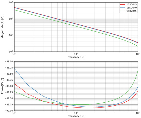
Figure 27.
Measured unbiased AC small-signal impedance plots for the three diodes between 100 and 10.
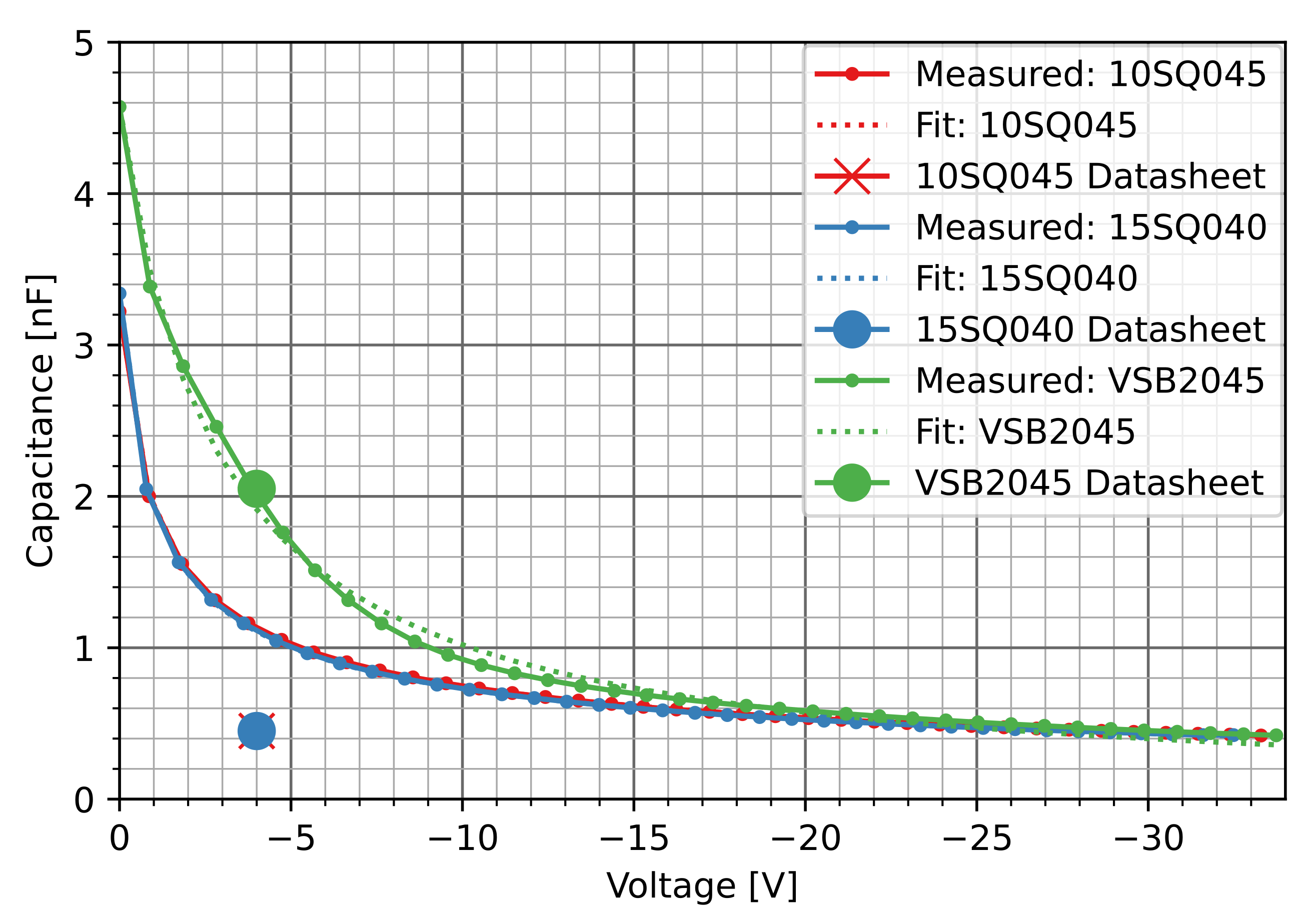
Prior to curve fitting of the voltage-dependent capacitance, the voltage drop over the 100 resistor in the DC Bias Tree circuit was compensated for. The resulting data took the form of Equation (15), where , , and are constants. Equation (15) was then fit to the measured data for the three diodes, and the resulting parameters for each diode are listed in Table 10. The measured and fit capacitance–voltage curves are shown in Figure 28, which illustrates the divergence between measured and datasheet parameters, as well as the differences between the fit and the measured capacitances. The best fit achieved was for the 10SQ045 diode, which had a mean absolute relative error of 0.2177%, followed by that of the 15SQ040 diode at 0.2733%, and finally the VSB2045 diode at 6.6779% (calculated over the full data range). Noteworthy is the difference between the measured data and the datasheet parameters. The 10SQ045 and 15SQ040 datasheet parameters indicate smaller capacitances than that which was measured; however, good agreement was achieved for the VSB2045 diode. A possible explanation for this is the fact that the diode datasheets are written for all the diodes in a series, as opposed to one diode model in particular. Therefore, an average capacitance is expressed by the manufacturer, which is not always adequately representative. This highlights the importance of accurate measurement-based modelling in simulations. Also noteworthy is the good agreement between the zero-bias capacitance measurements obtained using the THT fixture in Table 9 of Section 3.2.1 and the capacitance measurements shown for a reverse bias of 0 shown in Figure 28. This agreement between separate test setups served as an additional validation step.
Table 10.
Capacitance modelling parameters for the three diodes.
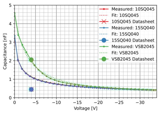
Figure 28.
Measured, fit, and datasheet reverse bias capacitances for the three diodes.
As initially introduced in Section 2.3.1, a capacitance measured using a small-signal based method describes a local capacitance, , which is therefore only appropriate for small-signal-based modelling. Equation (14), however, allows for the conversion of a local capacitance to a total capacitance, , which is appropriate for use with large-signal transient stimuli [26]. Thus, Equations (14) and (15) were combined, producing Equation (16). Equation (16) was then implemented in LTspice using the behavioural source-based method, as described in Section 2.3.1.
It was Equation (16) which was then input into LTspice as the governing equation for the dependent voltage source, C_Rep, in Figure 12.
At this point, all the required parameters for the proposed circuital model, capable of both forward and reverse bias, as well as both small-signal and large-signal dynamic operation, had been determined. Thus, the full circuital model could be constructed in LTspice.
4.5. Full Model Demonstrations
Operation of the LTspice implementation of the full circuital model, shown previously in Figure 12, is demonstrated in this section—firstly, by application of small-signal stimuli, and secondly, by application of large-signal transient stimuli.
4.6. Small Signal
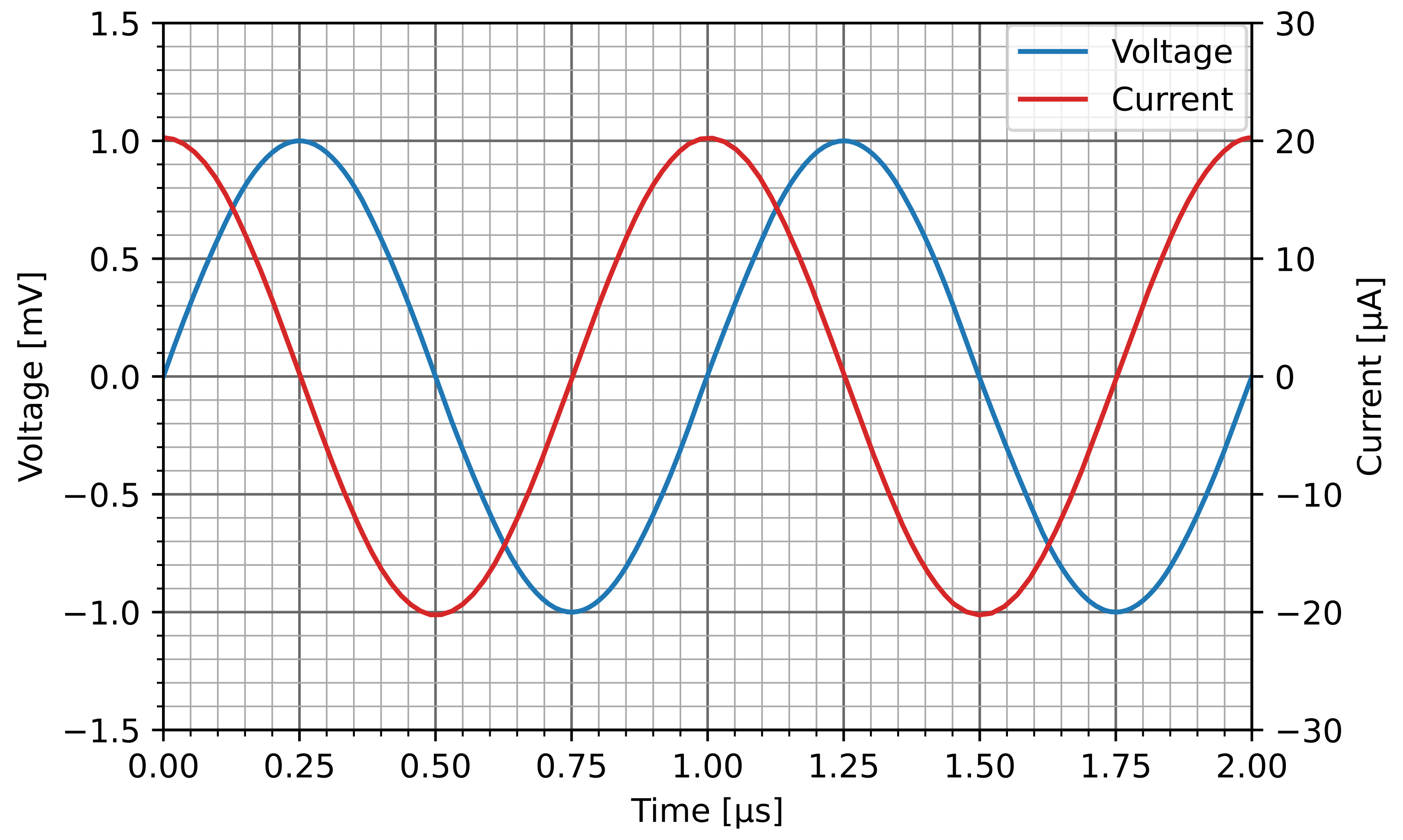
Small-signal operation of the full circuital model was demonstrated by applying a sinusoidal signal with an amplitude of 1 . In this demonstration, the parameters presented for the 10SQ045 diode were used. Figure 29 shows a time domain representation of the voltage over and current through the diode with the application of a 1 signal. As expected, the current through the diode was a sinusoidal signal (i.e., no rectification of the applied signal had occurred). The simulated current had a peak value of , with a phase angle (relative to the voltage waveform) of +90 deg. This produced an impedance of , which aligned with the measured and simulated small-signal impedance plot for the 10SQ045 diode seen previously in Figure 25 at 1 .
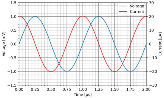
Figure 29.
LTspice simulated voltage and current plots for an input signal of 1 mV at 1 MHz.
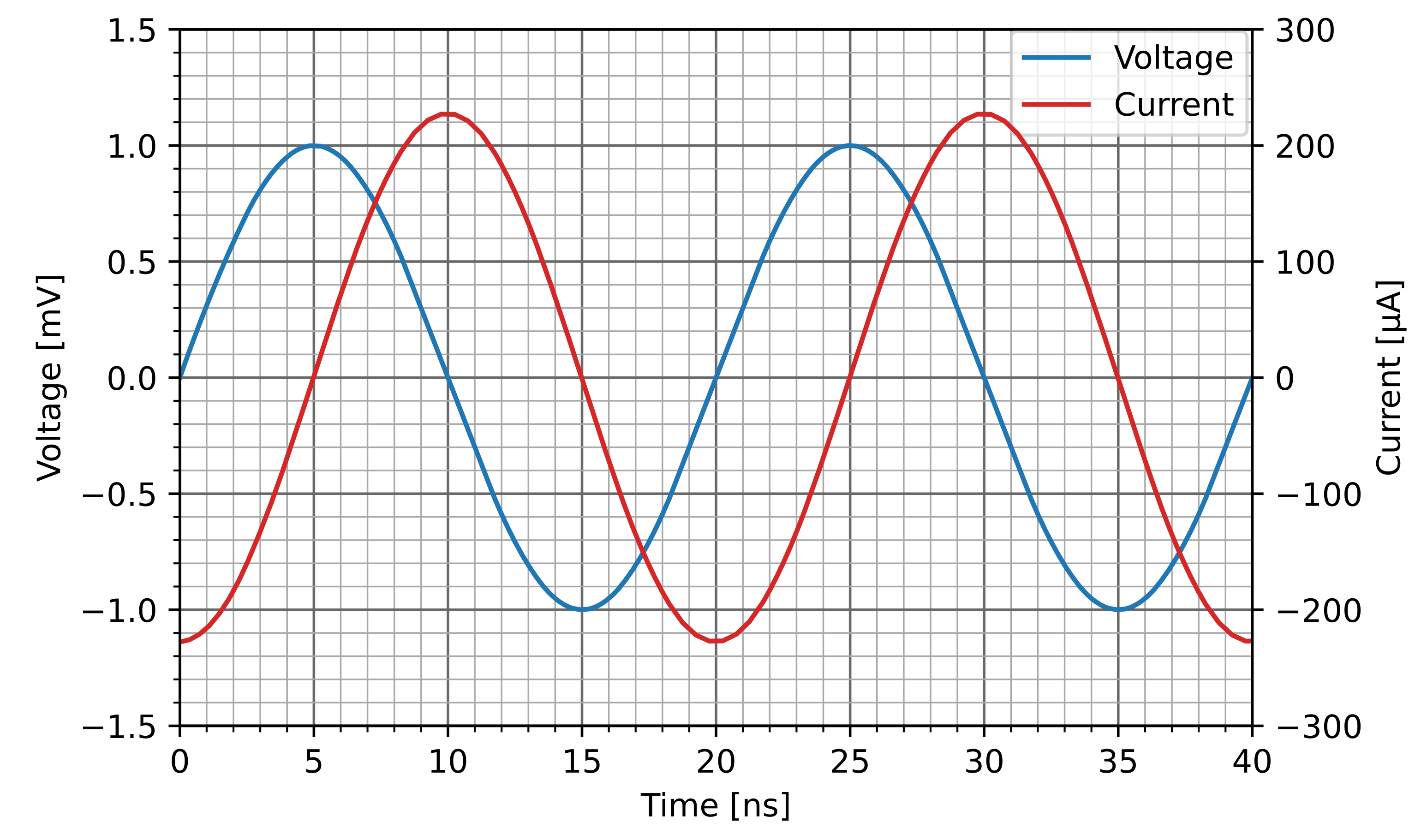
The frequency of the applied signal was then increased to 50 and the simulation was repeated. The simulated voltage and current curves are shown in Figure 30. Again, no rectification was observable, confirming small-signal operation. In this instance, the current through the diode had a peak value of , with a phase angle (relative to the voltage waveform) of +90. This produced an impedance of ; this also aligned with the impedance plot for the 10SQ045 diode seen in Figure 25 at 50 .
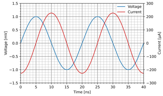
Figure 30.
LTspice simulated voltage and current plots for an input signal of 1 mV at 50 MHz.
5. Large Signal
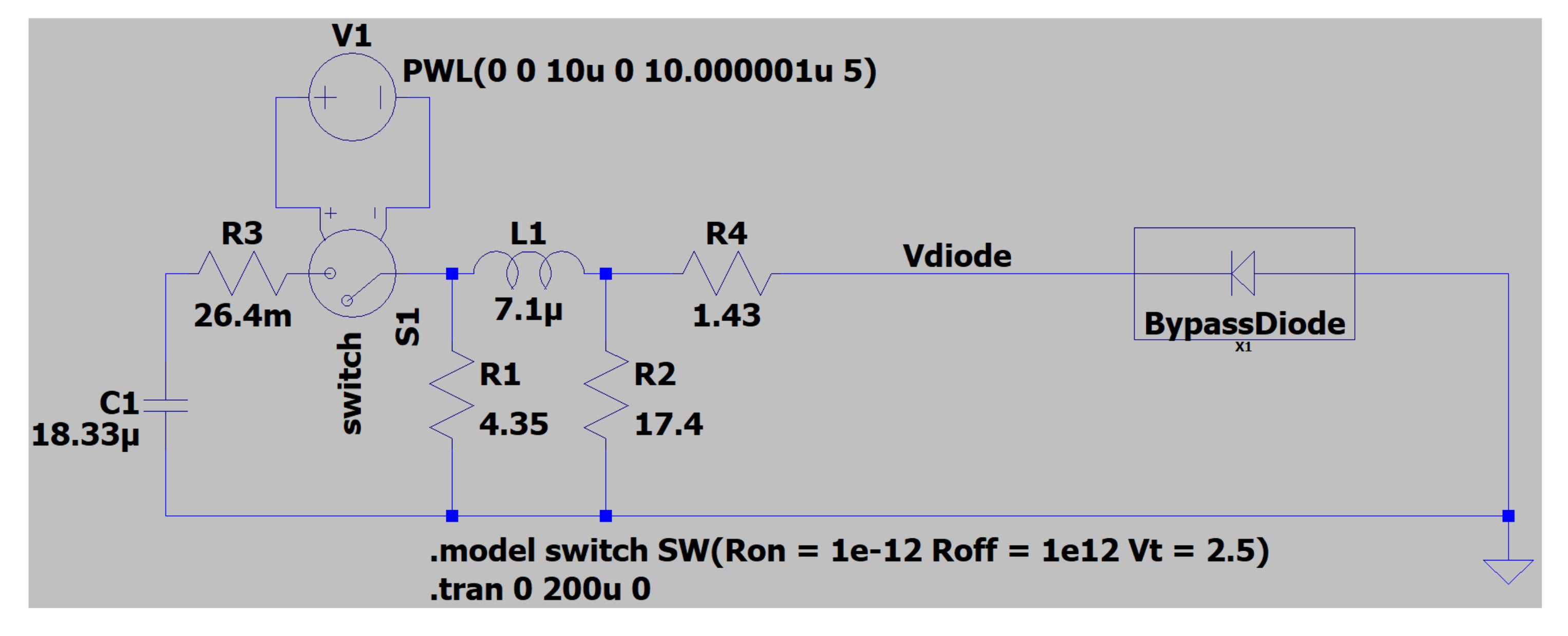
A model of a pulse generating circuit, similar to the desktop-scale setup in [13], was connected to the LTspice implementation of the full circuital model to demonstrate the response of the model to large-signal stimuli. This simulation setup is shown in Figure 31. In this setup, capacitor C1 is charged to an initial voltage of 250 , and has an equivalent series resistance represented by resistor R3. Switch S1 closes at time 10 , applying a pulse to the pulse-shaping circuit composed of resistors R1, R2, and R4, and inductor L1, and then to the full circuital model of the bypass diode.
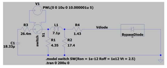
Figure 31.
LTspice large-signal stimulus test circuit, shown with the full circuital diode model in the reverse bias.
Figure 32 shows the simulated response of the full circuital diode model to the application of the pulse in the forward bias. As expected, the diode becomes forward-biased, conducting a large current pulse while exhibiting a small voltage drop.
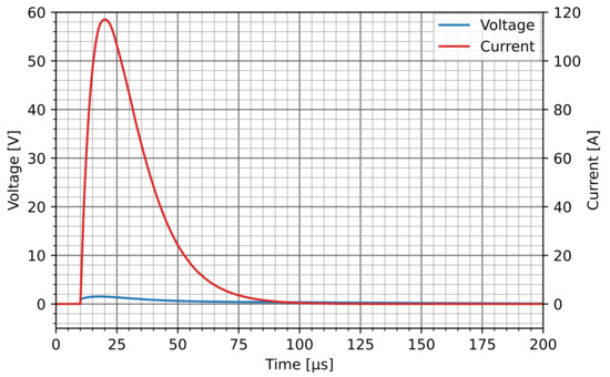
Figure 32.
LTspice simulated voltage and current plots for a large transient stimulus applied in the forward bias.
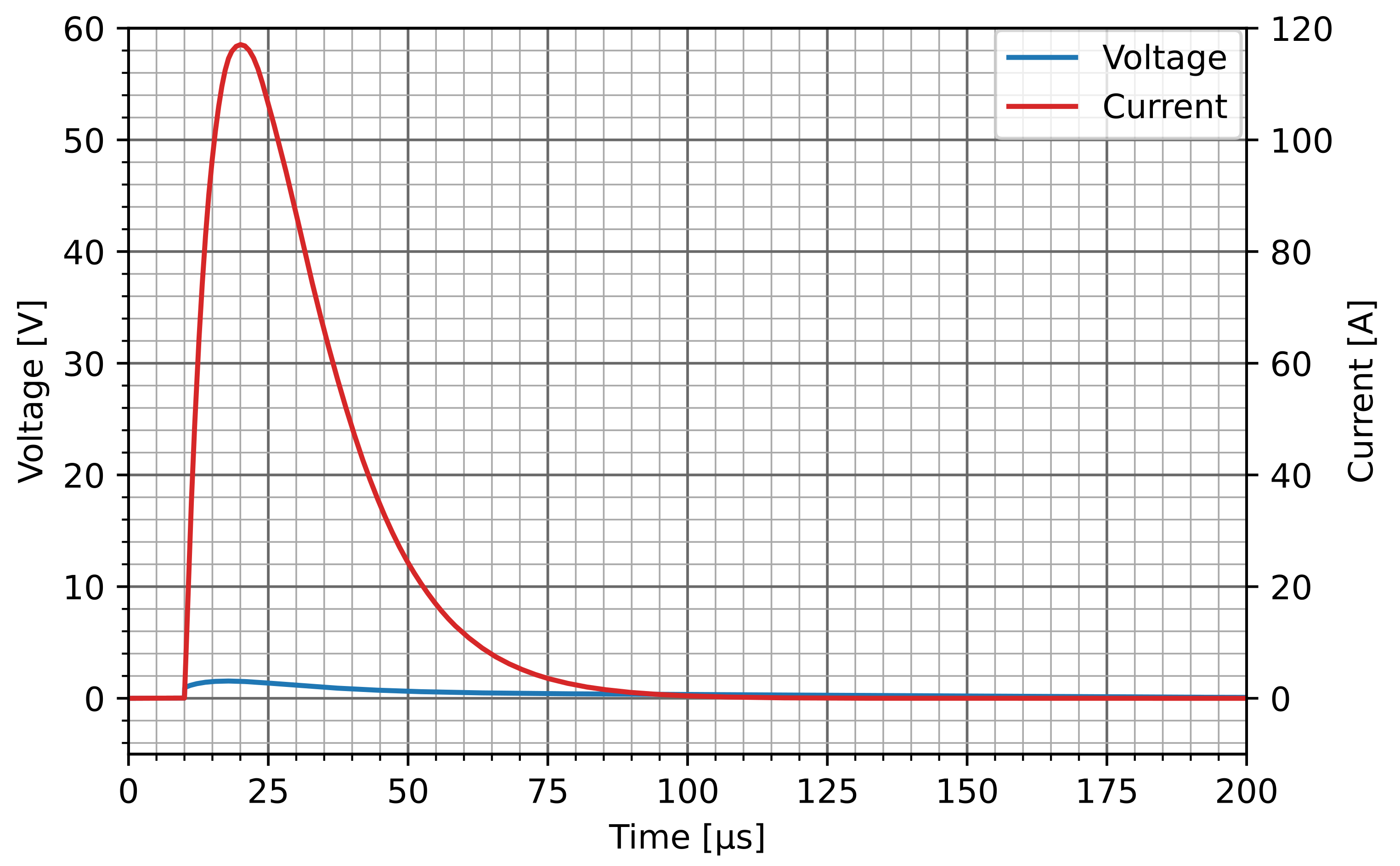
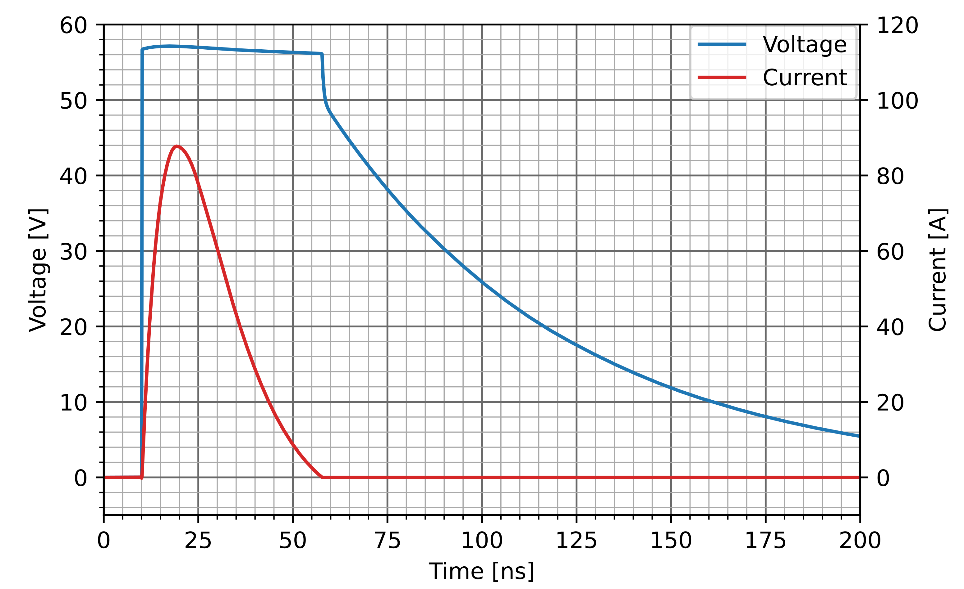
Figure 33 shows the simulated response of the full circuital diode model to the application of the pulse in the reverse bias. In this bias, a sharp voltage rise initially occurs, followed by a plateau at the breakdown voltage. Upon breakdown, a large current pulse then flows through the diode, while the voltage remains relatively stable. Subsequent to the conclusion of the current pulse, the voltage then gradually reduces.
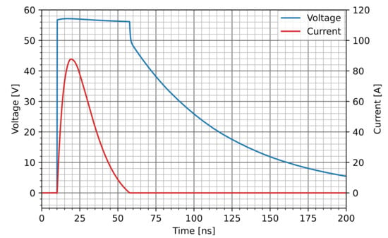
Figure 33.
LTspice simulated voltage and current plots for a large transient stimulus applied in the reverse bias.
The vertical axes for the forward and reverse bias plots above were purposefully fixed in order to clearly illustrate how the behaviour of the full circuital model differs depending on the applied bias. Should a linearised model be used for this purpose, as in [21], then the voltage and current waveforms would be identical for either bias. This would be an oversimplification of the behaviour of a device with strongly nonlinear characteristics. Thus, the implementation of an appropriate model is pivotal.
6. Discussion
This article presented a full circuital model, described in Section 2, as well as the required model parameters, in order to facilitate accurate SPICE-based modelling of three different Schottky diodes under dynamic conditions.
This model overcame the obvious limitations of previous studies involving simulations of large-signal transient surges in PV plants, where the bypass diodes were omitted or where their operation was overly simplified [13,14,15,16,22]. This model also overcame more subtle implementation-related limitations, such as the application of large-signal stimuli to small-signal models, by being constructed in such a way as to allow for the correct simulation of large-signal transients. For this, the correct application of the voltage-dependent capacitance, , was crucial. In addition, with the inclusion of the parallel leakage resistance, , and the reverse diode, , the presented model greatly improved the reverse bias current–voltage behaviour over that provided by the standard SPICE large-signal diode model. The resulting suitability to both small-signal and large-signal stimuli was demonstrated in Section 4.5.
It was important to the authors that the resulting model be SPICE-compatible, for two reasons: (1) as many SPICE-based simulators are open-source and/or free-to-use, this allows many researchers the chance to implement the proposed model in their research (without needing to purchase additional software licences), and (2) this ensured the greatest possibility of cross-compatibility with other simulation packages, which are focussed on other domains (such as CST Studio Suite 2021 by Dassault Systemes, an electromagnetic simulation package [33]). Knowing this, the model is bound by the limitations of SPICE, such as the inability to vary the component temperature throughout the simulation in a manner that is bidirectionally coupled to the electrical parameters. A MATLAB Simulink [34] model, such as in [4], based on first-principle operation, could overcome this limitation, but this would conflict with the accessibility and cross-compatibility intentions of the authors for this article.
Author Contributions
Conceptualization, K.M.C.; methodology, K.M.C.; software, K.M.C.; validation, K.M.C.; formal analysis, K.M.C.; investigation, K.M.C.; resources, K.M.C., P.G.W. and A.J.R.; data curation, K.M.C.; writing—original draft preparation, K.M.C.; writing—review and editing, P.G.W. and A.J.R.; visualization, K.M.C.; supervision, P.G.W. and A.J.R.; project administration, P.G.W. and A.J.R.; funding acquisition, P.G.W. and A.J.R. All authors have read and agreed to the published version of the manuscript.
Funding
This research received no external funding.
Institutional Review Board Statement
Not applicable.
Informed Consent Statement
Not applicable.
Data Availability Statement
Data used in this study are available upon request to the corresponding author.
Acknowledgments
The authors would like to thank (1) the Cape Peninsula University of Technology (CPUT) for the use of the OMICRON Lab Bode 100; (2) Florian Hämmerle and Tobias Schuster, of the OMICRON Lab, for the technical support relating to the use of the Bode 100; (3) Anneke Bester, of the Stellenbosch University Radio Frequency (RF) laboratory, for the use of ancillary technical equipment.
Conflicts of Interest
The authors declare no conflict of interest.
Appendix A. Bode 100 Signal Levels for Linear DUT Operation
The level of the signal at the output terminal of the Bode 100 is specified in . Specifying a source level in units of power is common in RF applications. In order to calculate the voltage at the output port, , the source impedance, , is required—which in this case is 50 . Should a load impedance of 50 be connected directly to the output terminal of the Bode 100, the power of the signal in watts at the output port can be calculated using Equation (A2). Equation (A3) can then be used to calculate . The voltage of the signal at the internal source, , can be calculated using Equation (A4), which is only valid for equal source and load impedances. A number of power levels are listed in Table A1, along with the corresponding voltages at the internal RF source and the output port.
Table A1.
Output power and corresponding voltages for a 50 system.
Table A1.
Output power and corresponding voltages for a 50 system.
| Power Level | Output Voltage (RMS) | RF Source Voltage (RMS) |
|---|---|---|
| [dBm] | [mV] | [mV] |
As the magnitude of depends on the voltage division between and , for an unknown nonlinear load, one needs to ensure that remains small enough to ensure linearity of the test setup at all frequencies within the measurement range, considering that as , .
Now that the RF source voltages corresponding to the power levels (in dBm) have been calculated, the worst-case scenario voltage at the DUT can be calculated for the measurement setup presented in Section 3.2.2. In order to calculate the highest possible , the following assumptions are made: (1) the impedance of the DC power supply, , and (2) the impedance of the capacitor, C, is negligible, which is true at high frequencies. As (i.e., when open-circuited), approaches the voltage at the essential node, , which joins , , and C. Following these assumptions, Equation (A5) can be used to calculate the maximum possible value of for different source levels.
For reference, a number of values for are presented in Table A2 below, along with the corresponding source levels. A common level for Schottky barrier diode capacitance testing is 50 pp [11]—this corresponds with an RMS level of at the DUT. Any of the source levels presented in Table A2 would therefore guarantee linear operation of the diodes.
Table A2.
Output power and corresponding voltages for the open-circuited measurement bridge.
Table A2.
Output power and corresponding voltages for the open-circuited measurement bridge.
| Power Level | RF Source Voltage (RMS) | (RMS) |
|---|---|---|
| [dBm] | [mV] | [mV] |
References
- Masters, G.M. Renewable and Efficient Electric Power Systems, 2nd ed.; Wiley-Interscience: Hoboken, NJ, USA, 2004; pp. 445–446. [Google Scholar]
- BYD Company. BYD P6C-36 Series-3BB; BYD: Shenzhen, China, 2013. [Google Scholar]
- Jordehi, A.R. Parameter estimation of solar photovoltaic (PV) cells: A review. Renew. Sustain. Energy Rev. 2016, 61, 354–371. [Google Scholar] [CrossRef]
- Kim, K.A.; Xu, C.; Jin, L.; Krein, P.T. A Dynamic Photovoltaic Model Incorporating Capacitive and Reverse-Bias Characteristics. IEEE J. Photovoltaics 2013, 3, 1334–1341. [Google Scholar] [CrossRef]
- Rauschenbach, H. Electrical output of shadowed solar arrays. IEEE Trans. Electron Devices 1971, 18, 483–490. [Google Scholar] [CrossRef]
- Kaushika, N.; Rai, A.K. An investigation of mismatch losses in solar photovoltaic cell networks. Energy 2007, 32, 755–759. [Google Scholar] [CrossRef]
- Vieira, R.G.; de Araújo, F.M.U.; Dhimish, M.; Guerra, M.I.S. A Comprehensive Review on Bypass Diode Application on Photovoltaic Modules. Energies 2020, 13, 2472. [Google Scholar] [CrossRef]
- ST Microelectronics. How to Choose a Bypass Diode for a Silicon Panel Junction Box; ST Microelectronics: Geneva, Switzerland, 2011. [Google Scholar]
- HY Electronic (Cayman) Limited. Schottky Barrier Rectifiers—10SQ030 thru 10SQ100; HY Electronic (Cayman) Limited: New Taipei City, Taiwan, 2014. [Google Scholar]
- DC Components Co. Ltd. 15SQ030 thru 15SQ100; DC Components Co. Ltd.: Taichung, Taiwan, 2013. [Google Scholar]
- Vishay Intertechnology Inc. VSB2045-M3; Vishay Intertechnology Inc.: Malvern, PA, USA, 2013. [Google Scholar]
- Coetzer, K.M.; Wiid, P.G.; Rix, A.J. The MOV as a Possible Protection Measure for Bypass Diodes in Solar PV Modules. In Proceedings of the 2019 International Conference on Clean Electrical Power (ICCEP), Otranto, Italy, 2–4 July 2019; pp. 286–291. [Google Scholar] [CrossRef]
- Coetzer, K.M. Investigating PV Module Failure Mechanisms Caused by Indirect Lightning Strikes. Master’s Thesis, Stellenbosch University, Stellenbosch, South Africa, 2019. [Google Scholar]
- Coetzer, K.M.; Wiid, P.G.; Rix, A.J. Investigating Lightning Induced Currents in Photovoltaic Modules. In Proceedings of the 2019 International Symposium on Electromagnetic Compatibility—EMC EUROPE, Barcelona, Spain, 2–6 September 2019; pp. 261–266. [Google Scholar] [CrossRef]
- Coetzer, K.M.; Wiid, P.G.; Rix, A.J. PV Installation Design Influencing the Risk of Induced Currents from Nearby Lightning Strikes. In Proceedings of the 2019 International Conference on Clean Electrical Power (ICCEP), Otranto, Italy, 2–4 July 2019; pp. 204–213. [Google Scholar] [CrossRef]
- Tu, Y.; Zhang, C.; Hu, J.; Wang, S.; Sun, W.; Li, H. Research on lightning overvoltages of solar arrays in a rooftop photovoltaic power system. Electr. Power Syst. Res. 2013, 94, 10–15. [Google Scholar] [CrossRef]
- La Manna, D.; Li Vigni, V.; Riva Sanseverino, E.; Di Dio, V.; Romano, P. Reconfigurable electrical interconnection strategies for photovoltaic arrays: A review. Renew. Sustain. Energy Rev. 2014, 33, 412–426. [Google Scholar] [CrossRef]
- Kim, K.A.; Krein, P.T. Reexamination of Photovoltaic Hot Spotting to Show Inadequacy of the Bypass Diode. IEEE J. Photovoltaics 2015, 5, 1435–1441. [Google Scholar] [CrossRef]
- Roehr, W.D. Rectifier Applications Handbook; ON Semiconductor: Tokyo, Japan, 2001; Volume 3, pp. 49–87. [Google Scholar]
- B Sources (Complete Reference). Available online: http://ltwiki.org/?title=B_sources_%28complete_reference%29 (accessed on 12 October 2021).
- Formisano, A.; Hernández, J.C.; Petrarca, C.; Sanchez-Sutil, F. Modeling of PV Module and DC/DC Converter Assembly for the Analysis of Induced Transient Response Due to Nearby Lightning Strike. Electronics 2021, 10, 120. [Google Scholar] [CrossRef]
- Prajapati, M. Modeling and Analysis of EMI from DC Input of Photovoltaic Systems. Ph.D. Thesis, Nanyang Technological University, Singapore, 2019. [Google Scholar] [CrossRef]
- Python. Available online: https://www.python.org/ (accessed on 16 May 2022).
- Matplotlib: Visualization with Python. Available online: https://matplotlib.org/ (accessed on 16 May 2022).
- Neamen, D.A. Semiconductor Physics and Devices, 4th ed.; McGraw-Hill: New York, NY, USA, 2012; pp. 334–336. [Google Scholar]
- Zeltser, I.; Ben-Yaakov, S. On SPICE simulation of voltage-dependent capacitors. IEEE Trans. Power Electron. 2018, 33, 3703–3710. [Google Scholar] [CrossRef]
- LTspice Simulator. Available online: https://www.analog.com/en/design-center/design-tools-and-calculators/ltspice-simulator.html (accessed on 12 February 2022).
- Scipy.org. Available online: https://www.scipy.org/ (accessed on 1 October 2021).
- OMICRON Lab. Bode 100 User Manual ENU1006 05 03. Available online: https://www.omicron-lab.com/fileadmin/assets/Bode_100/Manuals/Bode-100-User-Manual-ENU10060503.pdf (accessed on 1 December 2021).
- OMICRON Lab. B-WIC & B-SMC Impedance Test Fixtures User Manual ENU 12480501. Available online: https://www.omicron-lab.com/fileadmin/assets/Bode_100/Accessories/Impedance_Adapters/B-WIC-B-SMC-UserManual-ENU12480501.pdf (accessed on 10 January 2022).
- Hu, C. Modern Semiconductor Devices for Integrated Circuits/Chenming Calvin Hu; Prentice Hall: Upper Saddle River, NJ, USA, 2010. [Google Scholar]
- Hämmerle, F. Bode 100 Application Note - Solar Cell Impedance Measurement V2.0. Available online: https://www.omicron-lab.com/fileadmin/assets/Bode_100/ApplicationNotes/SolarCell/App_Note_Solar_Impedance_V2_0.pdf (accessed on 2 November 2021).
- 3DS CST Studio Suite. Available online: https://www.3ds.com/products-services/simulia/products/cst-studio-suite/ (accessed on 15 May 2022).
- Simulink—Simulation and Model-Based Design. Available online: https://www.mathworks.com/products/simulink.html (accessed on 16 May 2022).


Publisher’s Note: MDPI stays neutral with regard to jurisdictional claims in published maps and institutional affiliations. |
© 2022 by the authors. Licensee MDPI, Basel, Switzerland. This article is an open access article distributed under the terms and conditions of the Creative Commons Attribution (CC BY) license (https://creativecommons.org/licenses/by/4.0/).