Abstract
This paper presents a two-stage DC/DC converter with high efficiency utilized in an electronic power conditioner (EPC), which is widely applicable in satellite communications, etc. The galvanically isolated converter contains two cascaded converters: a buck converter, which is a pre-regulator operating under a closed-loop condition, and a push–pull converter, which is intended to boost the input voltage, operating under an open-loop condition. In the push–pull converter, the power switches, including the main switches and the rectifier diodes, operate under zero-voltage switching (ZVS) and zero-current switching (ZCS) at both switch off and switch on, which minimizes the switching loss. Furthermore, all of the parasitic parameters, such as the parasitic capacitance, leakage inductance, and magnetizing inductance of the main transformer, are fully utilized. Therefore, the presented topology benefits from fewer semiconductors but higher efficiency. The proposed topology produces less EMI noise because of ZVS and ZCS processes whose fundamental switching frequency interference is relatively low. The presented converter achieves a wide bus voltage regulation range in a satellite because of the pre-regulation of the buck cell. The theoretical analysis is validated by a prototype and its experimental results. The maximum efficiency of the converter can be up to 94.5%, and the high-voltage output is 7000 V.
1. Introduction
Microwave signals are amplified using space traveling wave tube amplifiers [1] (STWTA) as an important component of satellite systems. Typically, a TWTA comprises a traveling wave tube [2] (TWT) and an electronic power conditioner [3] (EPC). An interaction between a beam wave and an electromagnetic wave contributes to the amplification of microwave power when a TWT is utilized. Additionally, the EPC converts the satellite bus voltage [4] (typically ranging from 30 to 100 V DC) to the required electrode voltage (ranging from a few kV to a few hundred kV DC) through high-frequency power converters. Since the primary power conversion is the most significant aspect of the EPC, it must be considered when designing the circuit [5].
Presently, the main power conversion is categorized into two major types: single-stage power conversion and two-stage power conversion. The greatest advantage of single-stage conversion is its simplicity, and it is used in applications such as phase-shifted full-bridges [6,7,8], asymmetric half-bridges [9,10,11], three-transistor push–pulls [12], and so on. However, all of these single-stage topologies suffer from the same issue: stringent input voltage and load quality requirements. The application of a single-stage power conversion cannot satisfy the requirements of satellites. Consequently, two-stage power converters are increasingly utilized in the EPC. There are two types of topologies that have become dominant applications: boost and full-bridge [13], and buck and phase-shifted full-bridge [14]. In boost and full-bridge topologies, the control loop response time is very slow, and the surge current is high [15]. Furthermore, the complexity of the control systems of buck and phase-shifted full-bridge converters negatively impacts their reliability, and this topology cannot work in ZVS or ZCS when the load is not heavy [16]. Two other two-stage cascade transformations, flyback and asymmetrical half-bridge, and forward and push–pull, are rarely used due to their poor efficiency. In these two-stage topologies, forward and push–pull have the highest efficiency, which is 91.47% [17].
The statistics indicate that STWTAs consume 70% to 90% of DC consumption. Additionally, they contribute to 35% of the total weight in radar systems [18]. Therefore, power conversion topology must be continuously enhanced to meet the requirements of higher efficiency [19] and the miniaturization of on-board equipment.
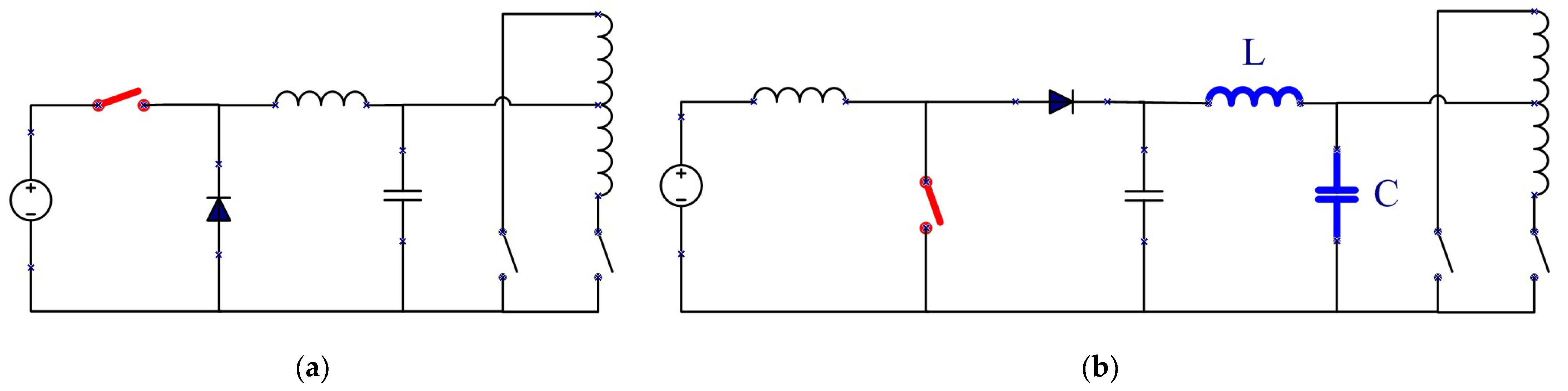
Buck and push–pull, and boost and push–pull are two different topologies, as shown in Figure 1. Based on the system requirement, if EPC has some malfunctions or failures, it cannot affect other modules in the satellite. If in the fault mode, the power switch (the red one) in Figure 1a can be turned off and thus can prevent affecting the bus voltage in the satellite. However, in Figure 1b, the power switch (the red one), when turned off, cannot prevent affecting the bus voltage, and it must include an additional protective circuit. Moreover, if ZVS and ZCS need to be realized in a boost and push–pull topology, extra inductance and capacitance (the blue ones) need to be added to the circuit, which increases the complexity of the circuit.
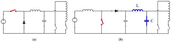
Figure 1.
The two different topologies of a two-stage converter: (a) The buck and push–pull topology, and (b) the boost and push–pull topology.
Motivated by the above analysis and practical application, this paper presents a two-stage converter topology with a high efficiency: buck and push–pull, where the push–pull converter is implemented in ZVS and ZCS. The buck regulator is used to pre-regulate the voltage in hard switching.
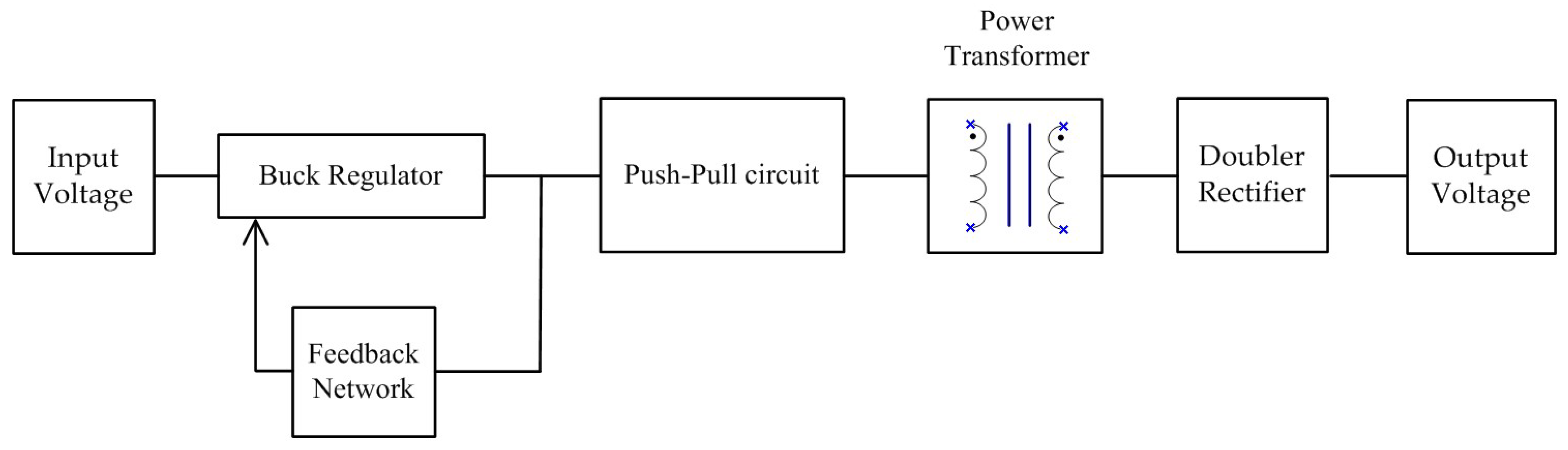
In addition, the high-voltage output is achieved through a soft-switching push–pull converter. The block diagram of this two-stage converter is shown in Figure 2. Closed-loop feedback is applied in the buck regulator to provide stable voltage for the push–pull circuit, and the push–pull circuit works in an open-loop state with a high output voltage after a doubler rectifier circuit.
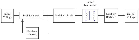
Figure 2.
The block diagram of the two-stage converter.
This two-stage DC/DC converter topology enjoys the following advantages:
(1) It makes full use of the parasitic capacitance and inductance that participate in the resonant switching, without adding additional components, in order to achieve soft switching and thereby increase efficiency.
(2) The power switches of the push–pull converter and the diodes of the second side of the rectifier can be operated to provide zero current and zero voltage both at the time of switching off and switching on, resulting in increased efficiency and reduced voltage and current limitations.
(3) Dual interleaved drivers are used in the buck circuit, so the magnetic reset process does not need to be considered for duty cycles that exceed 50%, and the design of the drive transformer is more compact than that of a single-drive method, resulting in a significantly broader range of applications.
(4) This topology produces less EMI noise due to the shapes of the current and voltage waveforms, which contain very low magnitudes of fundamental switching frequency interference.
(5) The cost is lower as a result of the low-current/voltage limitation (also a result of point 1), and it is simple to implement overload limitation without causing component damage.
(6) The control scheme can be simpler than full-bridge or other topologies if the switches in both the buck and push–pull operate on the same frequency.
This paper begins with Section 2, which examines operational modes. Section 3 introduces the key parameter utilized in the topology design. Section 4 presents the experimental results from the laboratory prototype. Section 5 compares buck and push–pull converters with other topologies and discusses potential future research enhancements. Section 6 concludes the paper.
2. The Proposed Converter
2.1. Description of the Topology
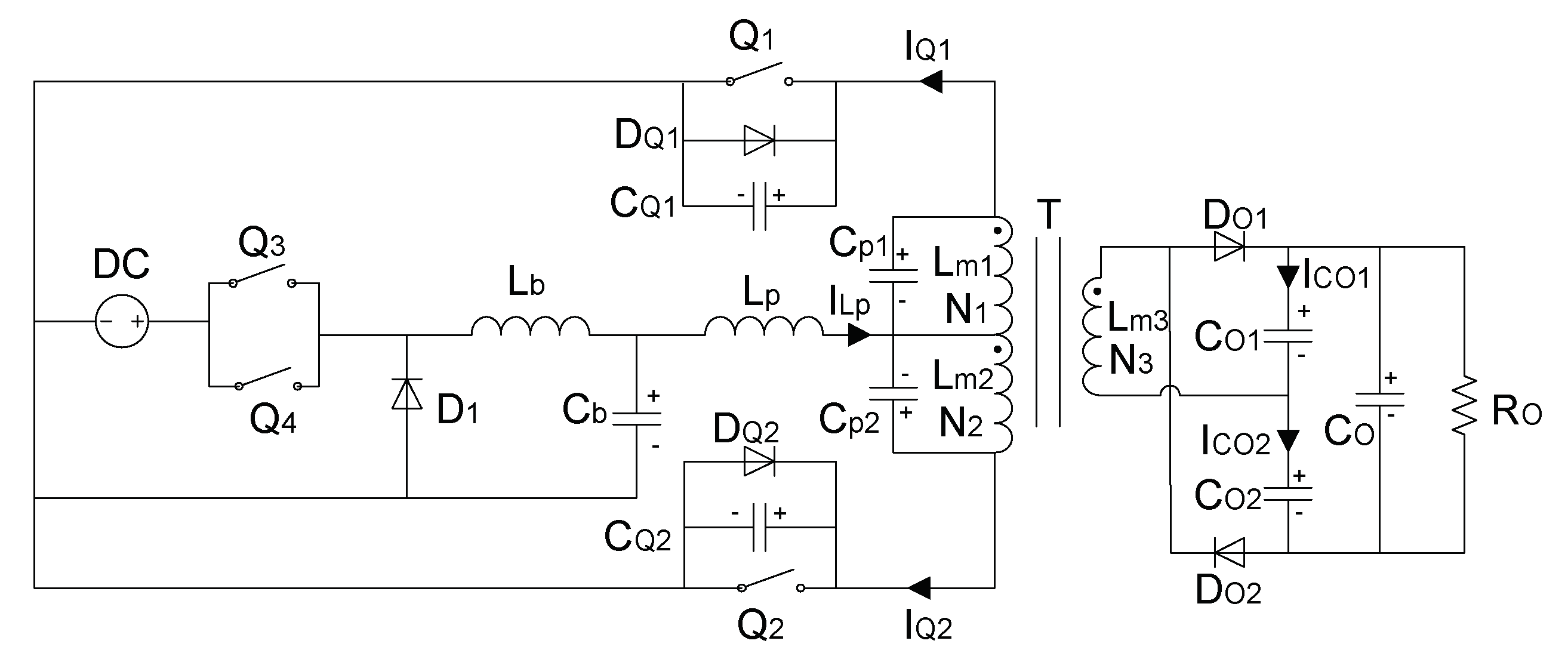
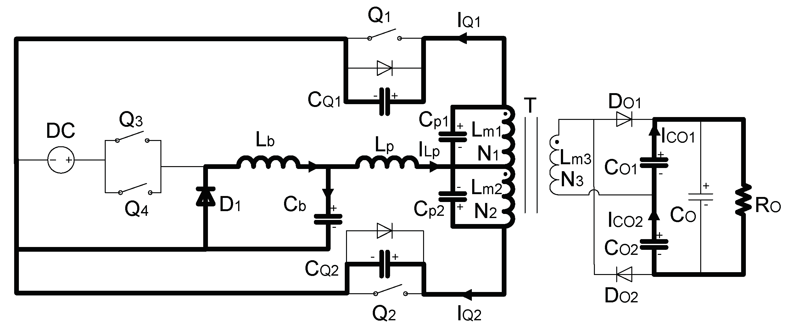
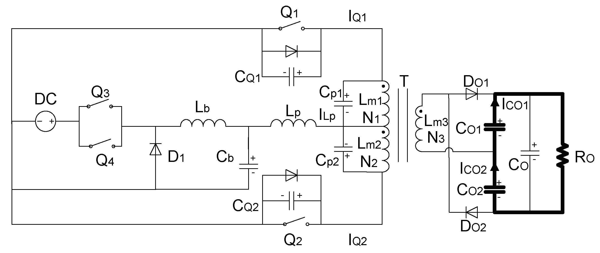
This paper proposes a two-stage DC/DC converter consisting of a buck regulator and a push–pull converter. The schematic circuit is depicted in Figure 3.

Figure 3.
The DC/DC converter circuit diagram.
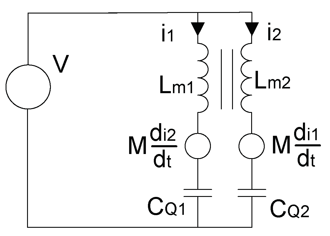
, , , , and constitute the interleaved dual-driver buck regulator. They are power switches, the fly-wheel diode, inductance, and capacitance, respectively. Equivalent primary leakage inductance, , helps achieve the soft-switching with , as will be discussed later. The resonant frequency is . and are power switches used in push–pull converter. The transformer, T, provides galvanic isolation between the input and output sides and is employed to generate high voltage together with voltage-doubler circuits, which include voltage-doubler rectifier diodes and capacitance: , , , and . Winding capacitance, and , cannot be ignored because the converter is applied in a high-voltage situation. and denote the sums of the parasitic output capacitance of the semiconductor and external parallel capacitance. and are body diodes.
The following considerations are made to make the analysis simpler:
(1) Assume that all components are ideal;
(2) Transformer turns ratio, :
where is much larger than ;
(3) The sum of semiconductor parasitic output capacitance and external parallel capacitance:
(4) Voltage-doubler rectifier capacitance
and the voltage of both and are .
2.2. Modes of Operation
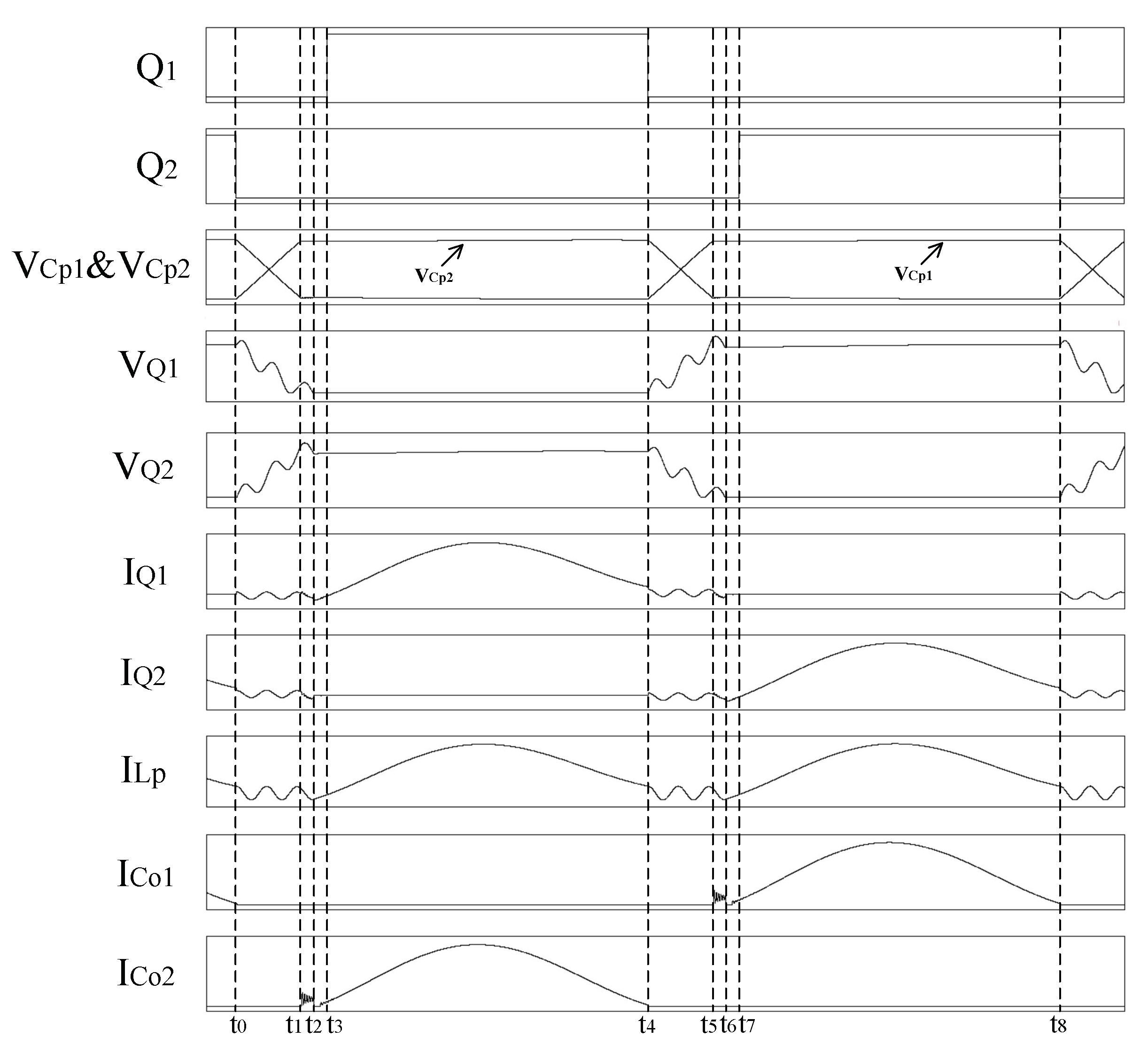
Throughout the process of a completed switching cycle, from ~, the converter operates in eight modes, as in the following exposition. The key waveforms are exhibited in Figure 4.
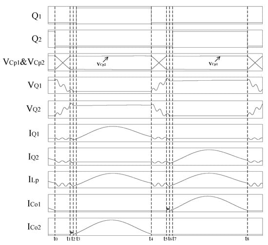
Figure 4.
The key waveforms in a complete switching cycle.
Mode I [, ]: The equivalent circuit of mode I is depicted in Figure 5. The switch turns off at the instant of , the capacitance starts to charge, and the voltage increases. On the other hand, is discharging simultaneously. Furthermore, the charging capacity of is equal to the discharging capacity of due to the coupling effect and the balance of the transformer. There is no energy exchange in the transformer. The leakage inductance resonates with and . The winding capacitance of transformer starts charging and discharges. In addition, . When the voltage of reaches , reaches and this mode comes to the end.
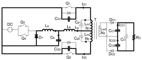
Figure 5.
The equivalent circuit of mode I.
Since there is no energy exchange between the primary side and the secondary side in mode I, the voltage across can be considered constant, and the equivalent circuit of mode I can be depicted in Figure 6.
Figure 6.
Approximated equivalent circuit for no energy exchanging between the primary side and secondary side.
Therefore:
As , , neglecting the effect of the leakage inductance, it is , so that yields:
Combining (5) and (6):
The solution of (7) is:
Mode II [,]: The equivalent circuit of mode II is depicted in Figure 7. In this mode, the voltage of winding capacitance remains , and remains . keeps charging, and the voltage increases. Since is discharging, the voltage decreases as well. A small level of high-frequency oscillated current flows through the second-side rectifier diode . When the voltage of drops to 0 and rises to , and complete discharging and charging and mode II finishes.
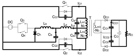
Figure 7.
Equivalent circuit of mode II.
Mode III [,]: The equivalent circuit of mode III is depicted in Figure 8.When the resonance on the primary side of the transformer finishes, the current through , , , and returns to 0, but the voltage is still the same, respectively. and go to 0 gradually so that the MOSFET operates in ZCS when it turns on. From the moment of , the current through returns to 0, and operates in ZCS in the stage of energy exchange between the primary and secondary sides.
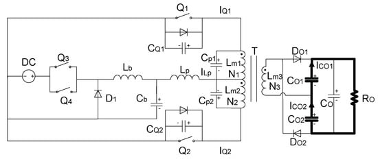
Figure 8.
Equivalent circuit of mode III.
Mode IV [,]: As had already been 0 at , the MOSFET turns on in ZVS. Mode IV is the major process that transfers energy from the primary side to the secondary side. No more current flows in , , , or , but the voltage on them is invariable. Energy transmits from the push–pull side to the high-voltage side through a high-frequency transformer on the coupling of magnetizing inductance . The current in increases gradually in sinusoidal form from 0 to the maximum (about 10 A), then decreases to 0 later again, the current in charges the voltage-doubling capacitance in the same form and synchronously offers energy for the load. In the current circumstance , the MOSFET operates in ZCS when it turns off, and mode IV comes to an end.
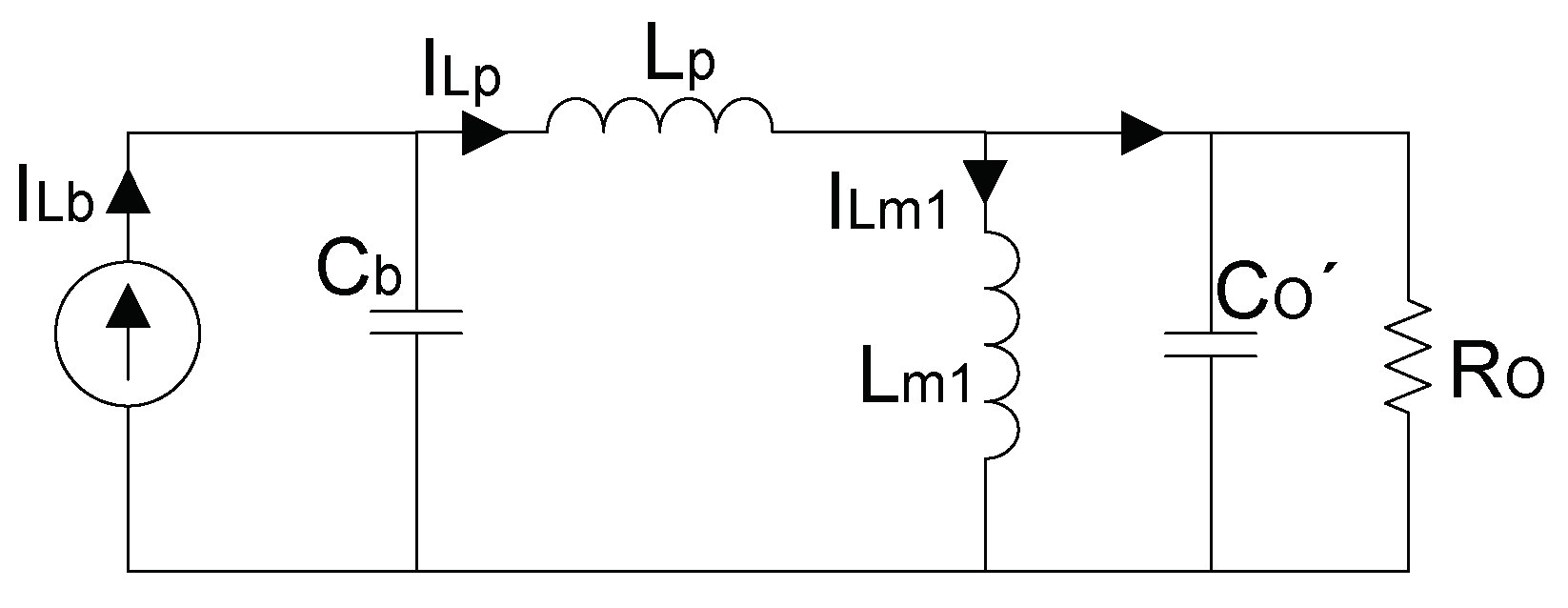
The equivalent circuit of Figure 9 can be depicted in Figure 10 during the time that switch is on. Normally, the equivalent output capacitance, , is much smaller than the buck capacitance, , so the main resonance can be located in the loop consisting of and leakage inductance, . According to KCL,
Hence,
whose solution is:
According to KVL,
that is,
Applying (11) into (13):
whose solution is:
Until the moment , the first half of the switching cycle comes to an end, and the circuit turns into the second half of the cycle. Based on symmetry, modes V~VIII are in one-to-one correspondence with modes I~IV.
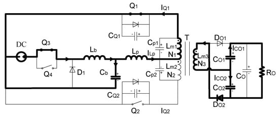
Figure 9.
Equivalent circuit of mode IV.
Figure 9.
Equivalent circuit of mode IV.
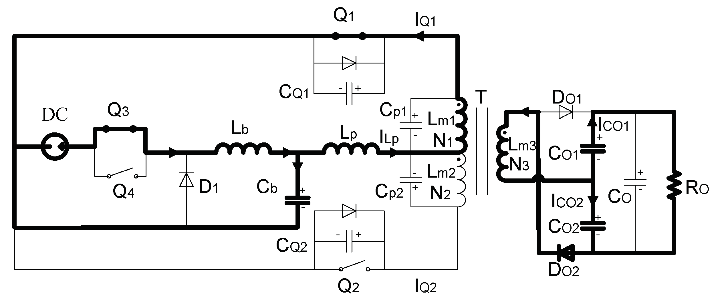
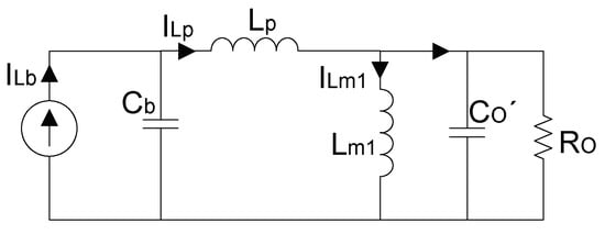
Figure 10.
When the switch turns on, this circuit is equivalent to the circuit in Figure 9.
Figure 10.
When the switch turns on, this circuit is equivalent to the circuit in Figure 9.
3. Key Parameter Design
Taking input voltage , output voltage , load power , and switch frequency as an example, the key parameter design of the circuit is as follows.
3.1. Buck Inductance,
Buck inductance can be calculated as:
where is the voltage of buck output (V), in this case, ; is the duty cycle (%) in the interleaved dual-driver, ; is the ripple current rate, , generally; is the current of the buck output (A), and . Hence, .
3.2. Buck Capacitance,
Buck capacitance can be calculated as:
where is the leakage inductance of the transformer and is the switching frequency.
3.3. Power Transformer Parameter
The number of turns on the primary side of the transformer is:
where is the waveform factor of the square wave; is the switching frequency; the type of magnetic core is TPW33-UYF36 series; is the magnetic flux density; and is the effective cross areas of the core. Therefore, . Taking an integer value, that is .
The number of turns on the secondary side of the transformer can be calculated by
In this case, .
The general design rule of the power transformer parameter is that the equivalent primary leakage inductance, , and the winding capacitance of the transformer, , should be suitable. The practical measurements of these parasitic parameters: and . If is different from the design value, a switch frequency of can be achieved by adjusting the value of the buck capacitance, , according to . If the sum value of , , and the external parallel capacitance is about 10 nF, ZVS and ZCS are realized in the two-stage converter.
3.4. Power Loss of Transformer
Allowable loss can be calculated as:
where is the total loss (W), is the total copper loss (W), is the copper loss of the primary side (W), is the copper loss of the secondary side (W), and is the average length of a single turn (cm).
The actual loss can be calculated as:
where is the weight of allowable iron loss (kg).
Obviously,
The loss in the unit area can be calculated as:
The temperature increase in the transformer is less than 20 °C in this case. The coiling method of the transformer additionally obtains a smaller distributed capacitance in layer coiling mode than in slot coiling mode, which has just a couple of nF.
3.5. Interleaved Dual-Driver Isolated Transformer
Buck circuits use interleaved dual drivers that require the support of an isolated driver transformer. The leakage inductance and power loss are reduced as a result of the use of the RM5 series of ferrite magnet cores and the “hamburger” coiling method, in which the primary side coil is wrapped by two secondary side coils. The calculation of drive transformer turns is identical to that of power transformer turns.
4. Experimental Validation
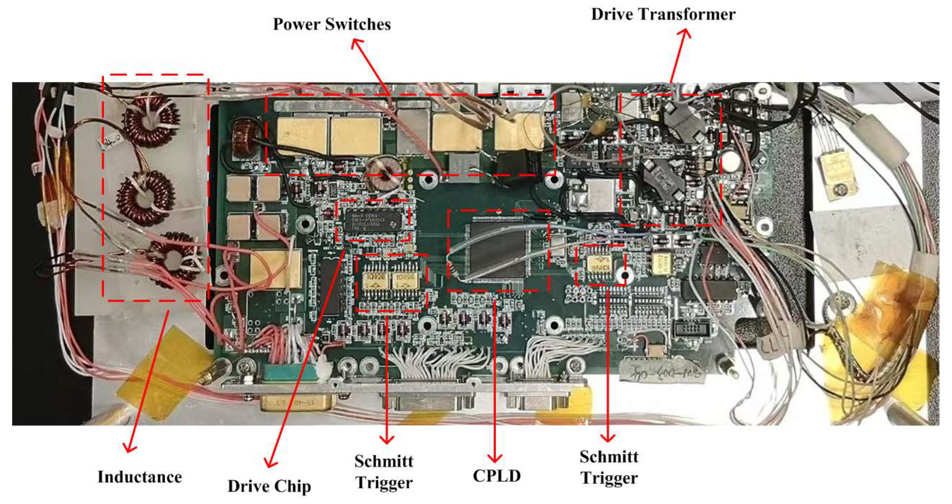
As shown in Figure 11, a laboratory prototype of the EPC was fabricated to verify the ZVS and ZCS in the two-stage DC/DC converter, along with other characteristics. In the converter, there are four power switches: two switches are used in the buck regulator and another two switches are used in the push–pull circuit. The driver transformer is used to isolate the drive signals because the source electrodes of power switches in the buck circuit connect to the non-zero level. The inductances include one buck inductance and two filter inductances in input voltage. CPLD is used to generate control signals and control the sequence relationships.

Figure 11.
Experimental EPC in the laboratory.
Dual interleaved drivers are used in the buck circuit, and the driving frequency of the buck regulator is consistent with that of the push–pull circuit. The single-channel drive frequency is 45.2 kHz, and the equivalent switching frequency of the dual interleaved drivers is 90.4 kHz. The drive signals are applied to the power switches of the buck circuit through the drive chip and the isolated drive transformer. Table 1 outlines the parameters.

Table 1.
Parameters of the converter.
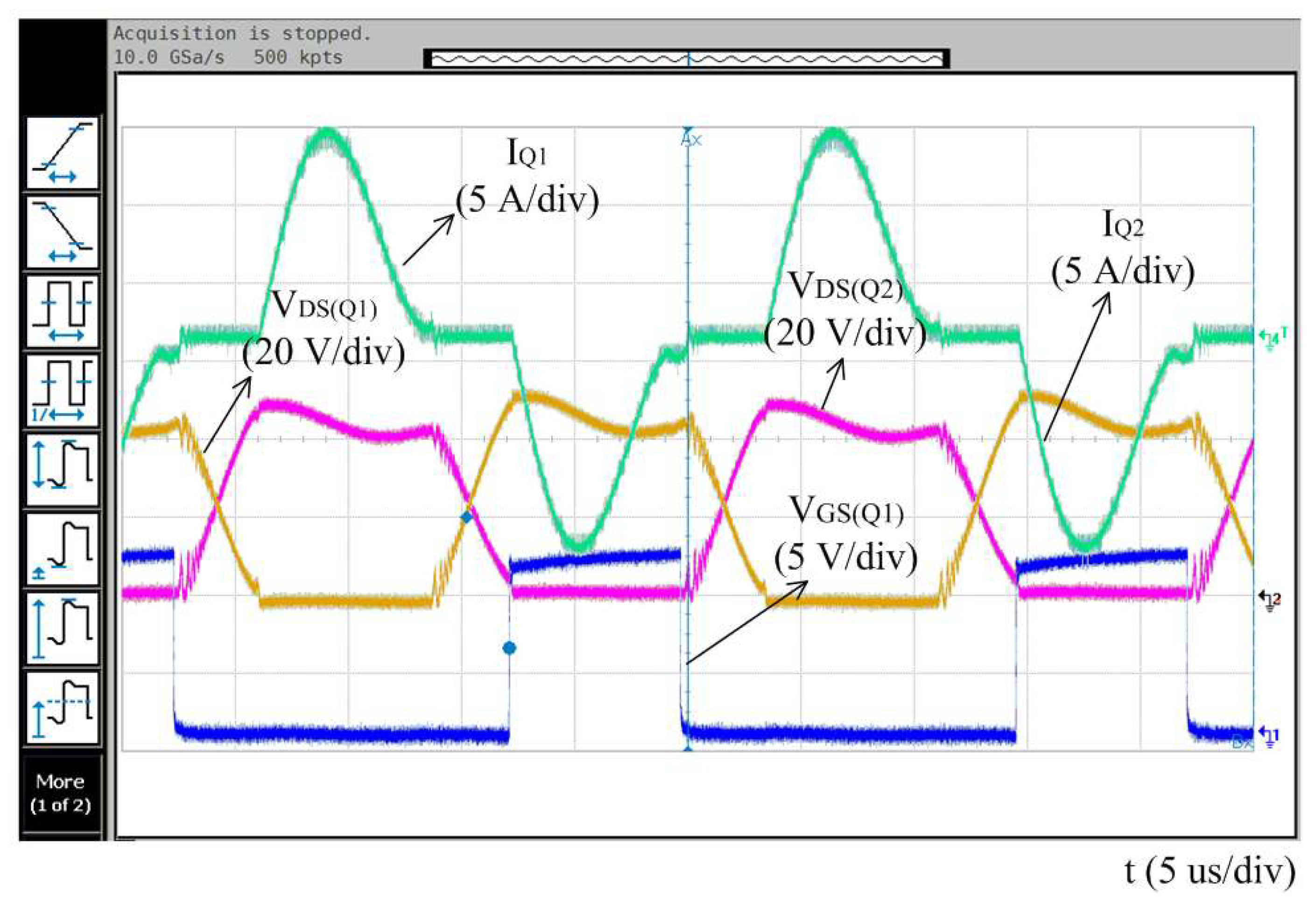
Figure 12 shows that ZVS and ZCS can be realized in both the on and off states. The waveforms of both and are approximately trapezoidal, and and are sinusoidal. There is no voltage spike or overshooting current. The peak voltage of the switches:
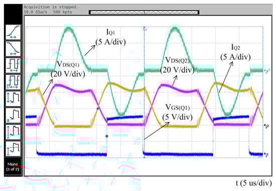
Figure 12.
Steady-state waveforms of the converter.
The voltage stress is independent of the load. The peak current of the switches:
where is the operating frequency of dual interleaved drivers, which is 90.4 kHz, is the off time of the switches, which is 14.9 us, while is the on time of the switches, which is 7.38 us.
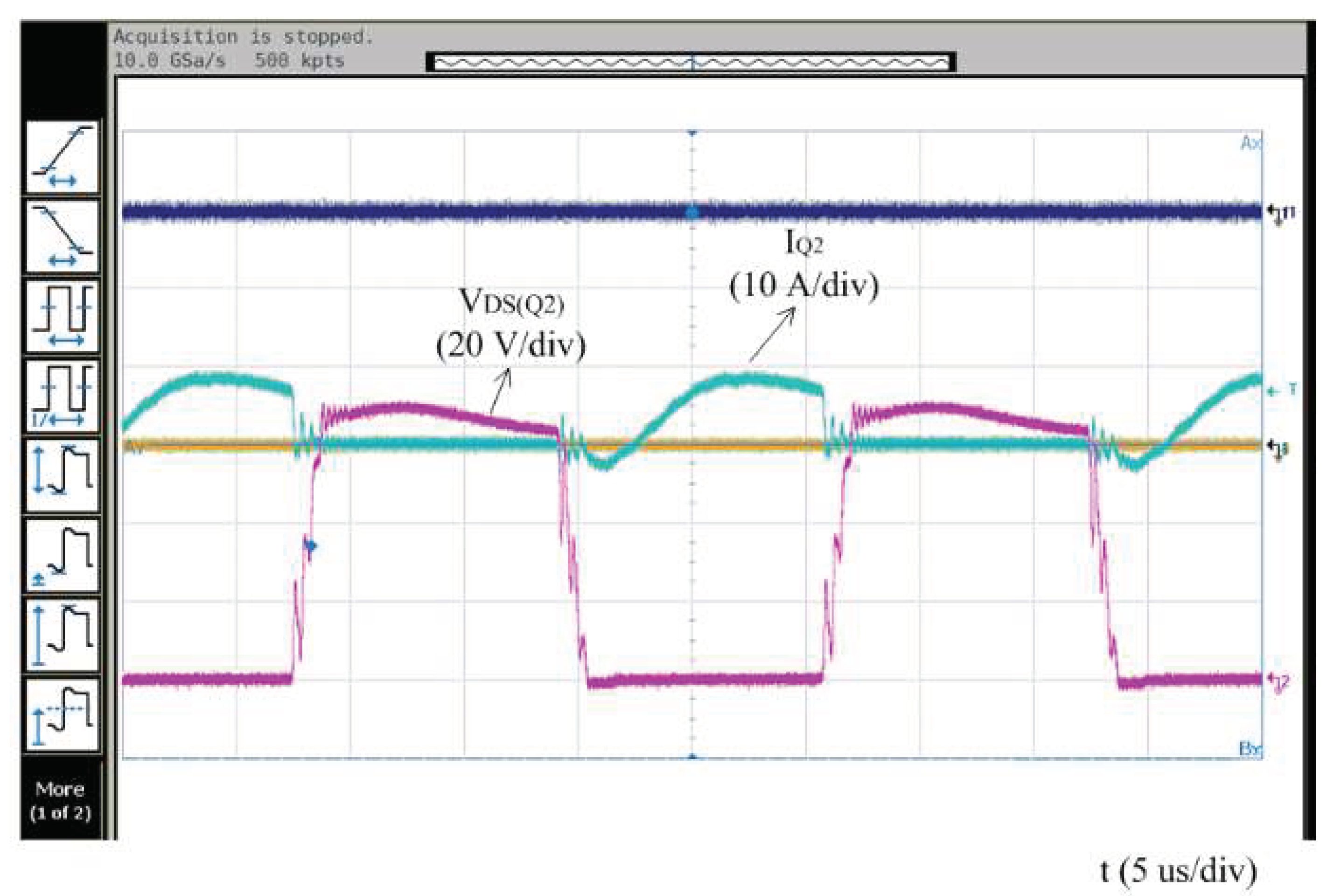
In the same load condition (130 W), the parasitic capacitance and leakage inductance are used to form the resonant tank. Moreover, another two-stage converter, boost and push–pull, can realize ZVS but cannot realize ZCS. The drain-source voltage also increases and reaches 70 V, as shown in Figure 13.
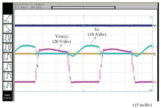
Figure 13.
The waveform of another two-stage converter, boost and push–pull. The load is 130 W.
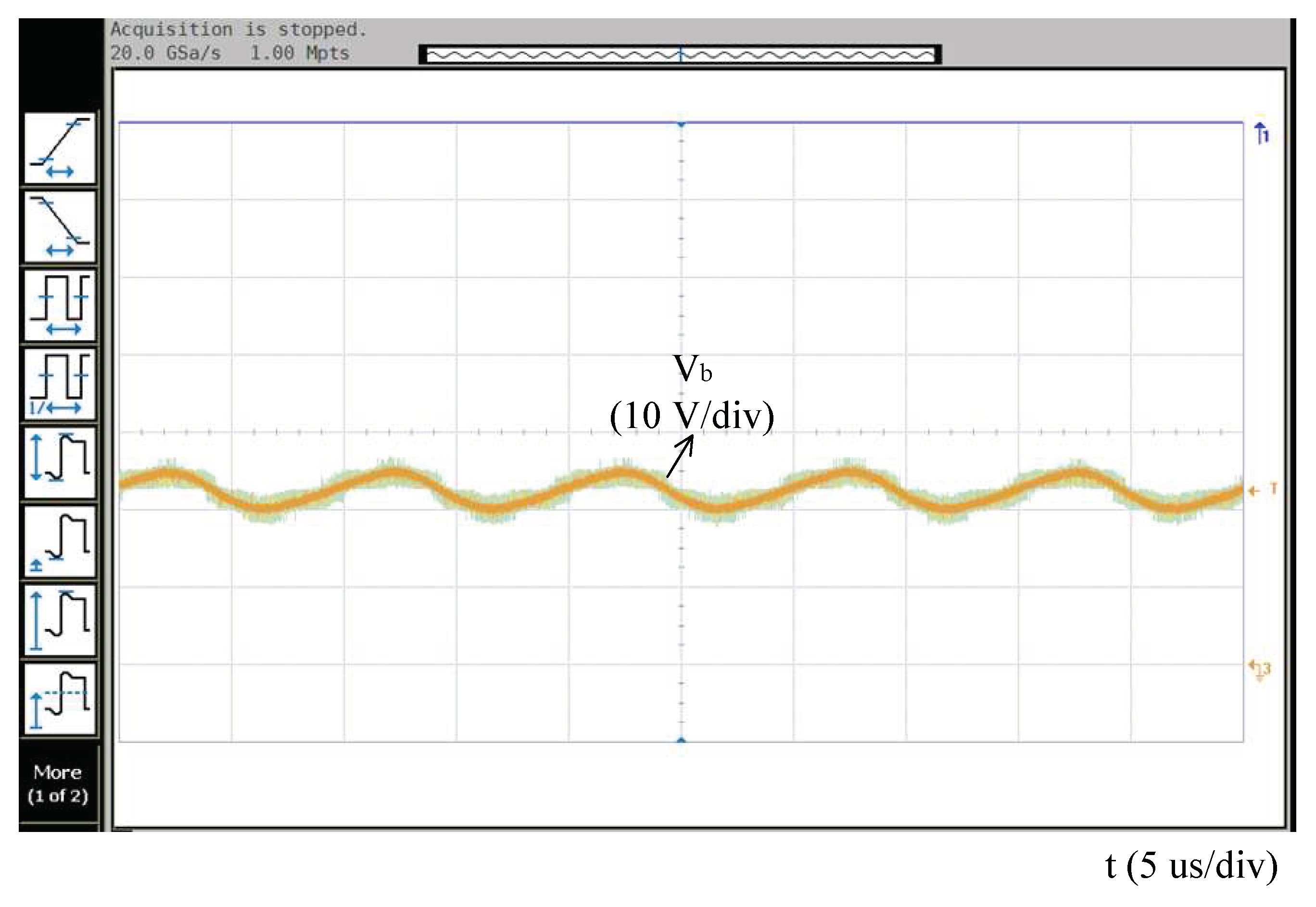
According to Figure 14, the buck voltage is about 22 V in the two-stage converter.
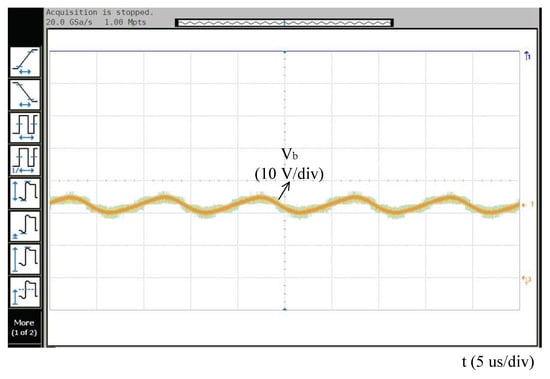
Figure 14.
The waveform of buck voltage, .
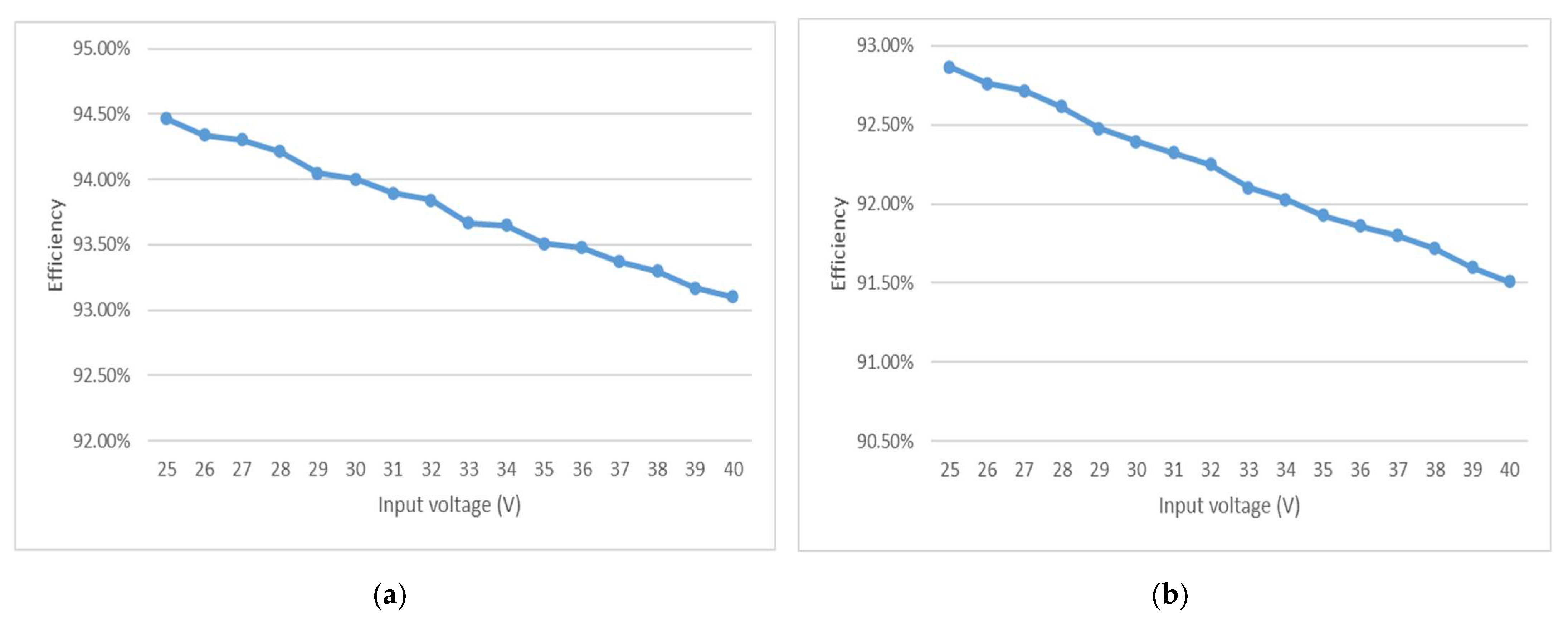
The bus voltage in satellites always varies, but the target of high efficiency never changes. Figure 15 illustrates the variation in efficiency in different input voltages, where Figure 15a illustrates the efficiency when the output power is 130 W, while Figure 15b shows the efficiency when the output power is 75 W. The lower input voltage or the heavier load leads to a higher duty cycle for the buck converter. As a result, the efficiency of the DC/DC converter increases as well. The highest efficiency can be up to 95%.
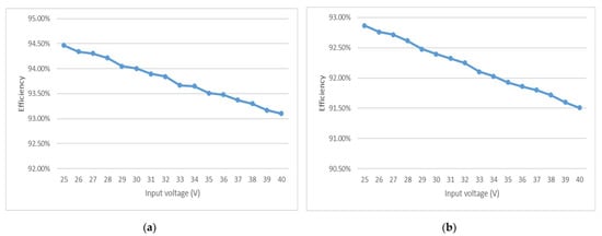
Figure 15.
The efficiencies of the converter in different input voltages for different loads: (a) The efficiencies for 130 W; (b) The efficiencies for 75 W.
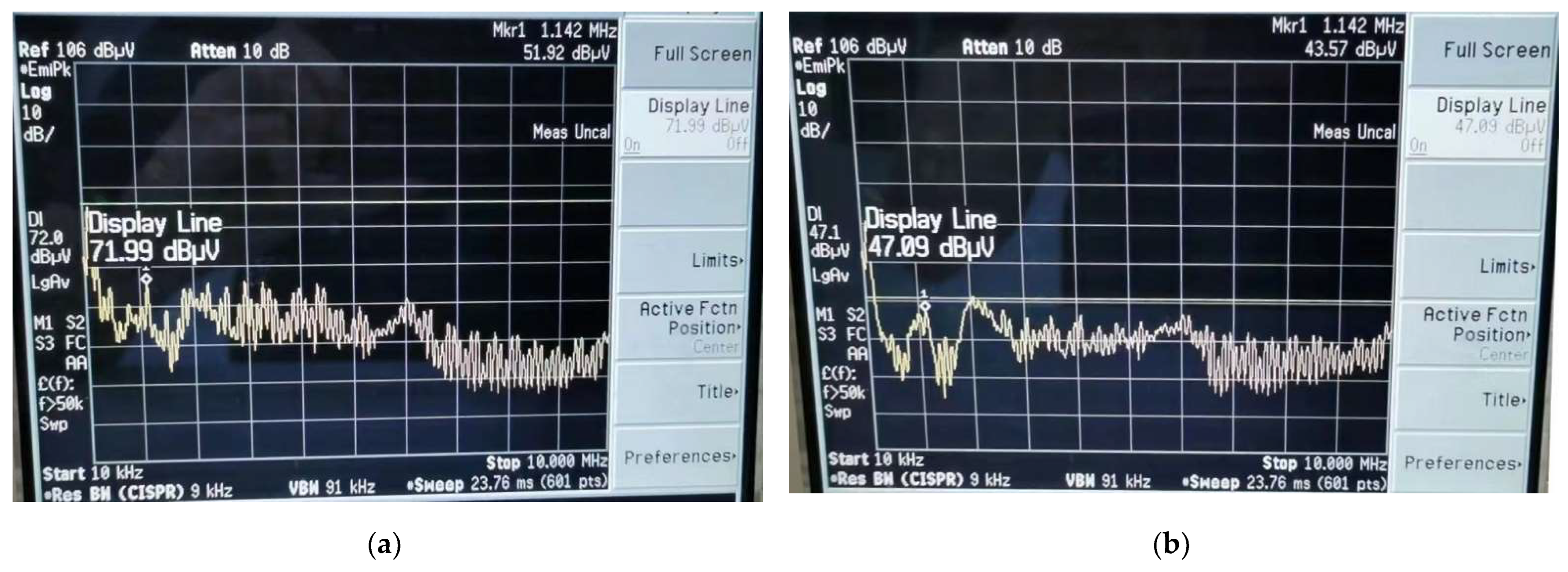
Figure 16 shows the test result of the conducted emission of this two-stage converter in different switching conditions, where Figure 16a presents the test result when the converter worked in hard switching, while Figure 16b shows the result when the converter worked in soft switching. According to the test results of conducted emission, when the converter worked in ZVS and ZCS, the interference of conduction emission was smaller than that in hard switching.
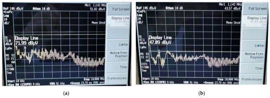
Figure 16.
The test result of conducted emission in different switching conditions: (a) The two-stage converter in hard switching; (b) The two-stage converter in soft switching.
5. Discussion
According to the experiment results, the buck and push–pull converter works in ZVS and ZCS in both the off and on states. Another two-stage converter, boost and push–pull, can realize ZVS but not ZCS under the same load condition (130 W), and the drain-source voltage also increases.
Compared with a unipolar topology, this two-stage topology can operate steadily in ZVS and ZCS over a wider input voltage range from 25 V to 40 V. When the input voltage ranges from 24 V to 30 V, unipolar topologies, such as three-transistor push–pull, can realize ZVS and ZCS [12].
Another common two-stage converter is forward and push–pull. The forward and push–pull converter can realize ZCS or zero-current transition (ZCT) using resonant components on the secondary side of the transformer. ZCS causes high current stress, and its efficiency is low. ZCT operates in quasi-resonance mode, which may result in low current stress; the efficiency is relatively higher; and the maximum efficiency is 91.47% when operating at full load [17]. Compared with forward and push–pull, the buck and push–pull converter can achieve up to 94.5% efficiency.
However, the two-stage converter has many aspects that need to be improved. In subsequent work, the planar transformer will be considered for a further reduction in volume, and the lower ripple of the output voltage needs to be researched continuously.
6. Conclusions
In this paper, a two-stage DC/DC converter, buck and push–pull, was proposed. The proposed power converter was studied based on circuit analysis. In addition, a prototype was built, and the theoretical analysis was validated by the experimental results. The proposed two-stage converter enjoys the following advantages:
(1) All parasitic parameters, including the leakage inductance, magnetizing inductance, and parasitic capacitance, are fully utilized in the proposed two-stage power converter. Only an external resonant capacitance is required for the resonant tank. Therefore, fewer components are needed.
(2) In addition, all power switches, including the main switches and the rectifier diodes, operate under ZVS and ZCS. As a result, the switching loss is minimized, which contributes to the increase in the switching frequency and efficiency. Experimental results show that the efficiency can reach 94.5%.
(3) Furthermore, the EMI issue is improved due to the soft switching advantages, which was validated by the experimental results.
In conclusion, a two-stage power converter was proposed, where the first stage is a buck converter and the second stage is a resonant push–pull converter. The working principles and the calculations of the main parameters were researched. The theoretical analysis was validated by a prototype. The experimental results show that the proposed topology is suitable for high-voltage, high-efficiency applications.
Author Contributions
Conceptualization, W.Z., X.-B.S. and G.W.; methodology, W.Z., X.-B.S., G.W. and B.Z.; software, W.Z. and X.-W.H.; validation, W.Z., C.H. and B.Z.; formal analysis, W.Z.; investigation, W.Z. and B.Z; resources, W.Z. and C.H.; data curation, W.Z. and C.H.; writing—original draft preparation, W.Z.; writing—review and editing, B.Z., X.-B.S., G.W., X.-W.H. and B.G.; visualization, C.H.; supervision, W.Z.; project administration, W.Z.; funding acquisition, W.Z. All authors have read and agreed to the published version of the manuscript.
Funding
This research received no external funding.
Institutional Review Board Statement
Not applicable.
Informed Consent Statement
Not applicable.
Data Availability Statement
Not applicable.
Conflicts of Interest
The authors declare no conflict of interest.
Nomenclature
The following is a list of symbols used in this paper and their meanings.
| Direct-current main | |
| to | Power switches |
| to | The sum of parasitic output capacitance of semiconductor and external parallel capacitance |
| to | Body diode |
| Power diode of buck regulator | |
| Inductance of buck regulator | |
| Capacitance of buck regulator | |
| T | Transformer |
| Equivalent primary leakage inductance of transformer | |
| Current of equivalent primary leakage inductance | |
| , | Winding capacitance of transformer |
| to | Magnetizing inductance |
| to | Transformer turns |
| , | Voltage-doubling rectifier diode |
| , | Voltage-doubling rectifier capacitance |
| , | Current of voltage-doubling rectifier capacitance |
| Output capacitance | |
| Output resistance | |
| Output voltage | |
| , | Commutated current of power switches in push–pull regulator |
| , | Drain-source voltage of power switches |
| Gate-source voltage of power switch |
References
- Wang, X.-N.; Su, X.-B.; Ma, D.-D.; Zhang, R.; Miao, G.-X.; Wang, W.-L. In-Orbit Reliability Evaluation of Space TWTA Based on Copula Function and Bivariate Hybrid Stochastic Processes. Appl. Sci. 2022, 12, 1575. [Google Scholar] [CrossRef]
- Wang, Y.; Dong, Y.; Zhu, X.; Guo, J.; Xu, D.; Wang, S.; Gong, Y. Multiple Dielectric-Supported Ridge-Loaded Rhombus-Shaped Wideband Meander-Line Slow-Wave Structure for a V-Band TWT. Electronics 2022, 11, 405. [Google Scholar] [CrossRef]
- Ivo, B.; Roger, G. Isolated DC-DC converters with high-output voltage for TWTA telecommunication satellite applications. IEEE Trans. Power Electron. 2003, 18, 975–984. [Google Scholar]
- Weinberg, A.H.; Ghislanzoni, L. A New Zero Voltage and Zero Current Power-Switching Technique. IEEE Trans. Power Electron. 1992, 7, 655–665. [Google Scholar] [CrossRef]
- Zhao, B.; Wang, G.; Hurley, W.G. Analysis and Performance of LCLC Resonant Converters for High-Voltage High-Frequency Applications. IEEE J. Emerg. Sel. Top. Power Electron. 2017, 5, 1272–1286. [Google Scholar] [CrossRef]
- Wu, S.; Liu, X. Research on Airborne Power Conversion Based on Phase-Shifting Full-Bridge. In Proceedings of the 11th International Conference on Computer Engineering and Networks (CENet2021) Part II, Hechi, China, 21–25 October 2021; pp. 96–104. [Google Scholar] [CrossRef]
- Kinnares, V.; Hothongkham, P. Circuit Analysis and Modeling of a Phase-Shifted Pulsewidth modulation Full-Bridge-Inverter-Fed Ozone Generator with Constant Applied Electrode Voltage. IEEE Trans. Power Electron. 2010, 25, 1739–1752. [Google Scholar] [CrossRef]
- Baek, J.; Kim, C.-E.; Lee, J.-B.; Youn, H.; Moon, G. A Simple SR Gate Driving Circuit with Reduced Gate Driving Loss for Phase-Shifted Full-Bridge Converter. IEEE Trans. Power Electron. 2018, 33, 9310–9317. [Google Scholar] [CrossRef]
- Kim, H.; Kim, J.; Kim, H.; Lee, K.; Kim, J.; Yoo, D.; Shin, D. A High Efficiency Photovoltaic Module Integrated Converter with the Asymmetrical Half-Bridge Flyback Converter. Sol. Energy 2010, 84, 1376–1381. [Google Scholar] [CrossRef]
- Mujjalinvimut, E.; Ayudhya, P.N.N.; Sangswang, A. An Improved Asymmetrical Half-Bridge Converter With Self-Driven Synchronous Rectifier for Dimmable LED Lighting. IEEE Trans. Ind. Electron. 2016, 63, 913–925. [Google Scholar] [CrossRef]
- Chowdhuri, S.; Biswas, S.K.; Talukdar, F.A.; Deb, N.K. Analysis and Design of an Asymmetrical Half Bridge Converter for Switched Reluctance Motor. J. Inst. Eng. (India) Electr. Eng. Div. 2002, 83, 78–80. [Google Scholar]
- Yao, Z.; Zhang, Y.; Hu, X. MOSFET-clamped three-level converters without flying capacitor. Int. Trans. Electr. Energy Syst. 2021, 30, e12218. [Google Scholar] [CrossRef]
- Yao, Z.; Liu, T. Boost and full-bridge integrated converter for wide input-voltage range application. Int. Trans. Electr. Energy Syst. 2021, 31, e12916. [Google Scholar] [CrossRef]
- Cai, J.; Zhao, L.; Wei, C.; Liang, J. Analysis of novel phase-shifted full-bridge converters with wide ZVS range reduced filter requirement: LETTER. IEICE Electron. Express 2022, 19, 20210391. [Google Scholar] [CrossRef]
- Jalbrzykowski, S.; Citko, T. Current-Fed Resonant Full-Bridge Boost DC/AC/DC Converter. IEEE Trans. Ind. Electron. 2008, 55, 1198–1205. [Google Scholar] [CrossRef]
- Zhao, L.; Li, H.; Wu, X.; Zhang, J. An Improved Phase-Shifted Full-Bridge Converter with Wide-Range ZVS and Reduced Filter Requirement. IEEE Trans. Ind. Electron. 2018, 65, 2167–2176. [Google Scholar] [CrossRef]
- Zhang, F.H.; Wang, H.Z.; Yan, Y.G. ZCT Scheme of Push-Pull Forward Converter. J. Southeast Univ. (Engl. Ed.) 2002, 18, 331–335. [Google Scholar] [CrossRef]
- Kowstubha, P.; Krishnaveni, K.; Ramesh Reddy, K. Electronic Power Conditioner for Ku-Band Travelling Wave Tube. J. Inst. Eng. (India) Ser. B Electr. Electron. Telecommun. Comput. Eng. 2017, 98, 213–220. [Google Scholar] [CrossRef]
- Katzir, L.; Shmilovitz, D. A 1-MHz 5-kV Power Supply Applying SiC Diodes and GaN HEMT Cascode MOSFETs in Soft Switching. IEEE J. Emerg. Sel. Top. Power Electron. 2016, 4, 1474–1482. [Google Scholar] [CrossRef]

Publisher’s Note: MDPI stays neutral with regard to jurisdictional claims in published maps and institutional affiliations. |
© 2022 by the authors. Licensee MDPI, Basel, Switzerland. This article is an open access article distributed under the terms and conditions of the Creative Commons Attribution (CC BY) license (https://creativecommons.org/licenses/by/4.0/).