Abstract
To broaden the absorption spectrum of cells, enhance the cell stability, and avoid high costs, a novel perovskite solar cell (PSC) with the structure of fluorine-doped tin oxide (FTO)/ZnO/CsPbI3/FAPbI3/CuSCN/Au is designed using the solar cell capacitance simulator (SCAPS) software. The simulation results indicate that the CsPbI3/FAPbI3 heterojunction PSC has higher quantum efficiency (QE) characteristics than the single-junction CsPbI3-based PSC, and it outputs a higher short-circuit current density (Jsc) and power conversion efficiency (PCE). In order to optimize the device performance, several critical device parameters, including the thickness and defect density of both the CsPbI3 and FAPbI3 layers, the work function of the contact electrodes, and the operating temperature are systematically investigated. Through the optimum analysis, the thicknesses of CsPbI3 and FAPbI3 are optimized to be 100 and 700 nm, respectively, so that the cell could absorb photons more sufficiently without an excessively high recombination rate, and the cell achieved the highest PCE. The defect densities of CsPbI3 and FAPbI3 are set to 1012 cm−3 to effectively avoid the excessive carrier recombination centering on the cell to increase the carrier lifetime. Additionally, we found that when the work function of the metal back electrode is greater than 4.8 eV and FTO with a work function of 4.4 eV is selected as the front electrode, the excessively high Schottky barrier could be avoided and the collection of photogenerated carriers could be promoted. In addition, the operating temperature is proportional to the carrier recombination rate, and an excessively high temperature could inhibit Voc. After implementing the optimized parameters, the cell performance of the studied solar cell was improved. Its PCE reaches 28.75%, which is higher than most of existing solar cells. Moreover, the open circuit voltage (Voc), Jsc, and PCE are increased by 17%, 9.5%, and 25.1%, respectively. The results of this paper provide a methodology and approach for the construction of high-efficiency heterojunction PSCs.
1. Introduction
Active layer materials of perovskite solar cells (PSCs) have a wealth of great properties such as high optical absorption capacity [1], long electron-hole diffusion length, low exciton binding energy, high power conversion efficiency (PCEs), and they are easy to process. [2,3]. Due to those advantages, PSCs have become a research hotspot in the field of photovoltaics. Some studies have reported PCEs of PSCs as high as 25.5% [4], which are comparable to those of silicon-based solar cells and indicate broad development prospects of PSCs.
The PCE of MAPbI3-based PSCs is limited by the wide bandgap of 1.58 eV. To further improve the PCE toward the theoretical limit above 30%, FAPbI3 with a narrow bandgap of 1.43 eV [5] is considered the promising perovskite material for high-performance single-junction PSCs, which fits better with the optimum value of ~1.4 eV for single-junction photovoltaics and displays extended light absorption toward the near-IR [6]. Mari-Guaita et al. [7] believed that for α-FAPbI3-based PSCs that use DMSO and DMF as the solvents, toluene would be the optimal antisolvent. Among the perovskite materials used in solar cells, the cesium-based all-inorganic halide perovskite CsPbI3 has a higher thermal stability than the commonly used organic–inorganic hybrid perovskite MAPbI3 [8]. Bouich et al. [9] proposed that CsPbI3 thin-films are suitable candidates for efficient, stable, and durable perovskite devices because CsPbI3-based PSCs can achieve high Voc due to its wider band gap. The replacement of MAPbI3 with CsPbI3 during the preparation of PSCs can improve the long-term stability of the cell under outdoor conditions [10]. However, compared with MAPbI3-based PSCs, CsPbI3-based PSCs output lower PCEs because CsPbI3 is prone to phase transitions, leading to relatively poor photoluminescence properties [11,12,13]. In addition, for single-junction photovoltaic cells, the band gap of CsPbI3 is not optimal (greater than 1.7 eV) [14,15].
Generally, single-junction solar cells cannot completely take advantage of photons with energies lower than the bandgap energy while thermalization loss occurs at the energy levels larger than the PCS bandgap [16]. To avoid the disadvantage of single junction CsPbI3, one effective method is to construct heterojunction structures which contain series of different perovskite materials that absorb in various regions of the light spectrum. Those structures are stacked on top of each other to provide bilayer or multilayer heterojunctions. Such structures can extract a wider energy range of spectrum from the sun light, thus, promoting the generation of photogenerated carriers and improving the PCE. Preparation of p-n perovskite heterojunction solar cells can break the single-junction Shockley–Queisser limit. The heterojunction between the two perovskite layers is widely regarded as a new paradigm in device engineering. For example, Lin et al. [17] proposed a novel energy band structure with MAPbI3/MAPbI2Br cascade layers and obtained 25.32% PCE. High-performance CsPbI3/XPbI3 (X = MA or FA) heterojunction perovskite solar cells were investigated by Akhtarianfar et al. [18], who believed that perovskite heterojunctions consisting of two different perovskite layers could make far-reaching changes in solar cell efficiency and stability. Li et al. [14] prepared α-CsPbI3/FAPbI3 bilayer active layer PSCs and showed that PCEs up to 15.6% could be harvested from the PSCs. The device stability was improved as well. A new hole transport layer (HTL) free PSC proposed with MAPbI3/CsSnI3 all-perovskite heterojunction as a light-harvester was proposed by Duan et al. [19], and the results revealed that the narrow band gap CsSnI3 broadens the absorption spectrum to the near-infrared region and the high hole mobility favors efficient hole transfer. Additionally, an all-inorganic perovskite-heterojunction CsPbI3/CsSnI3 is proposed as the absorber and the HTL-free CsPbI3/CsSnI3 was proposed as the absorber and the HTL-free CsPbI3/CsSnI3 PSCs were investigated systematically by Xu et al. [20]. As verified in their study, the proposed structure effectively extended the absorption range and enhanced its overall performance. Clark et al. [21] developed the sequential solution and processing method to fabricate a series of APbX3/MASnX3 (A = FA, MA, or Cs; X = I or Br) heterojunctions, which showed an enhanced device performance due to the heterojunctions.
PSCs with excellent performance often include carrier transport layers in their structural design. A carrier transport layer is divided into an electron transport layer (ETL) and a HTL, which is used to facilitate the transport of photogenerated electrons and photogenerated holes, respectively. In efficient PSCs, titanium dioxide (TiO2) and 2,2′,7,7′-tetrakis-(N,N-di-4-methoxyphenylamino)-9,9′-spirobifluorene (spiro-OMeTAD) are often used as the ETL and HTL, respectively. However, the preparation of TiO2 must be carried out in a high-temperature environment, which is not conducive to the preparation of flexible cells. Moreover, spiro-OMeTAD is expensive, which makes the preparation cost high, and its characteristics are unstable, which hinders the enhancement of the cell performance. These issues limit the large-scale promotion and application of PSCs. The latest research shows that inorganic materials possess outstanding stability and high carrier mobility [22]. Therefore, the use of inorganic materials as carrier transport layers to explore new materials that can be used as ETLs and HTLs is of significance for promoting the commercial application of PSCs.
Zhang et al. [23] discussed the application of zinc oxide (ZnO) as the ETLs in PSCs and introduced a method to prepare ZnO materials. Other related studies [24,25,26,27] have also confirmed the feasibility of using ZnO as the ETLs for PSCs. Azri et al. [28] compared inorganic materials, including nickel(II)oxide (NiO), cuprous thiocyanate (CuSCN), poly(3-hexylthiophene-2,5-diyl) (P3HT), and cuprous iodide (CuI), with spiro-OMeTAD, and the results revealed that when CuSCN was used as the HTL, the optimal cell performance was obtained. Madhavan et al. [29] used CuSCN as the HTL to prepare cells and obtained a PCE similar to that of spiro-OMeTAD. Murugadoss et al. [30] also confirmed that CuSCN can be used as the HTL for the preparation of PSCs.
In this study, the solar cell capacitance simulator (SCAPS) software was adopted to investigate the photovoltaic performances of heterojunction PSCs based on the previous findings. Three cell structures, fluorine-doped tin oxide (FTO)/TiO2/CsPbI3/spiro-OMeTAD/Au, FTO/TiO2/CsPbI3/FAPbI3/spiro-OMeTAD/Au, and FTO/ZnO/CsPbI3/FAPbI3/CuSCN/Au, were constructed and analyzed. The results showed that the performance of the cell with the structure of FTO/ZnO/CsPbI3/FAPbI3/CuSCN/Au could achieve a satisfactory performance while avoiding high fabrication costs and poor device stability. Based on this structure, the effects of the thickness and defect density of the photoactive layers, the work function of the contact electrodes, and the operating temperature on the performance of the cell were investigated. The Voc, Jsc, fill factor (FF), and PCE were used as evaluation indicators, combined with the quantum efficiency (QE), carrier concentration, and carrier recombination rate, to explore and optimize the key material parameters of CsPbI3/FAPbI3 heterojunction PSCs.
2. Methodology and Materials
2.1. Numerical Method
In this study, the one-dimensional SCAPS, developed by Professor Burgelman of Ghent University in Belgium [31], is used for the involved numerical modeling and simulation. SCAPS is based on the basic equations of semiconductor device physics. By combining the Poisson equation, the electron/hole continuity equations, and boundary conditions of the semiconductor device, the current, electric field distribution, and carrier concentration are determined. Finally, transport properties of the semiconductor device, such as J-V characteristics, spectral response, capacitance–frequency characteristics, and capacitance–voltage characteristics are obtained. The Poisson equation and the electron/hole continuity equations are expressed in the following equations [32]:
The drift-diffusion equations are presented as follows [33]:
where ε is the relative permittivity; and are the ionization acceptor concentration and ionization donor concentration, respectively; Ψ is the electrostatic potential; x is the position coordinate; pt and nt represent the concentrations of trapped holes and trapped electrons, respectively; p and n represent the concentrations of free holes and free electrons, respectively; Jn and Jp denote the photo-generated electron current density and photo-generated hole current density, respectively; Rn(x) and Rp(x) denote the recombination rate of electrons and holes, respectively; G(x) represents the photoproduction rate; q is the electron charge; μn and μp denote the mobility of electrons and holes, respectively; and Dn and Dp represent the diffusion coefficients of electrons and holes, respectively.
Under normal circumstances, these nonlinear differential equations (Equations (1)–(5)) are difficult to solve. However, if the boundary conditions, including the hole and electron current densities and the electric potentials at both ends of the device, are specified, the concentration of electrons and holes and the electric field can be determined, and other relevant operating parameters of the cell device can be obtained in turn. The potential at the back contact was set to 0, and the boundary conditions at the front contact are
The boundary conditions at the back contact are
In the above equations, the labels f and b represent the front electrode and the back electrode, respectively; Vapp denotes the bias voltage applied to the device or the bias voltage generated by the incident light; фf and фb represent the work functions of the front and back contact electrodes, respectively; peq and neq, respectively denote the hole and electron concentrations at the electrode interface under thermal equilibrium conditions; p′ and n′ are the carrier concentrations at the front and back contact electrodes, respectively; and , , , and represent the surface recombination rates of holes and electrons at the front and back electrodes, respectively, which are related to the surface passivation.
2.2. Device Structures and Input Parameters
In this research, three cell structures, FTO/TiO2/CsPbI3/spiro-OMeTAD/Au, FTO/TiO2/CsPbI3/FAPbI3/spiro-OMeTAD/Au, and FTO/ZnO/CsPbI3/FAPbI3/CuSCN/Au, are initially designed, as shown in Figure 1. For convenience of discussion, these three structures are referred to as Structures 1, 2, and 3, respectively. It can be seen from Figure 1 that the three structures are all planar upright structures, with FTO (work function 4.4 eV) and Au (work function 5.1 eV) as the front electrode and metal back electrode, respectively, and the light was incident from the FTO end. CsPbI3 is used as the photoactive layer in Structure 1, and commonly used TiO2 and spiro-OMeTAD are used as ETL and HTL, respectively. A main difference between Structures 1 and 2 is that in Structure 2, a heterojunction composed of CsPbI3 and FAPbI3 is used as the photoactive layer. In Structure 3, the same type of heterojunction is used as the photoactive layer, and inorganic materials ZnO and CuSCN are used as the ETL and HTL, respectively.
Figure 1.
Configurations of the initial perovskite solar cells (PSCs): (a) structure of TiO2/CsPbI3/spiro-OMeTAD, (b) structure of TiO2/CsPbI3/FAPbI3/spiro-OMeTAD, and (c) structure of ZnO/CsPbI3/ FAPbI3/CuSCN.
The energy level matching between the carrier transport layer and the photoactive layer has an impact on the output performance of the cell. In general, the top of the ETL valence band should be lower than the top of the valence band of the photoactive layer to avoid the transport of photogenerated holes in the direction of the ETL and reduce the carrier recombination. Similarly, the bottom of the conduction band of the HTL should be higher than the bottom of the conduction band of the absorption layer to prevent the photogenerated electrons from being transported in the direction of the HTL. When the bottom of the conduction band of the ETL is lower than the bottom of the conduction band of the photoactive layer and the top of the valence band of HTL is higher than the top of the valence band of the photoactive layer, the movement of photogenerated carriers is promoted, but the recombination rate of the interface could be high [34,35]. Studies have shown [36] that when the bottom of the ETL conduction band is 0.0–0.3 eV higher than the bottom of the conduction band of the photoactive layer and the top of the HTL valence band is 0.0–0.2 eV lower than the top of the valence band of the photoactive layer, although the transport of photogenerated carriers is inhibited, the cell can still show excellent performance due to the low interfacial recombination rate. A schematic diagram of the energy levels of the materials involved in the three structures is shown in Figure 2. In terms of the energy-level structure, the three cell devices presented in this paper are structurally feasible.
Figure 2.
Schematic diagram of material energy levels.
Following the approaches presented in authoritative literature [11,28,37,38,39,40], material parameters of TiO2, ZnO, CsPbI3, FAPbI3, CuSCN, and spiro-OMeTAD are set as shown in Table 1. To make the comparison of the results more convincing, in the initial models of the three structures, the thickness of the light-absorbing layer of structure 1, CsPbI3, is initially set to 600 nm, while the thicknesses of the light-absorbing layers of structures 2 and 3, CsPbI3 and FAPbI3, are both set to 300 nm so that the total thicknesses of the light-absorbing layers of the three structures were the same. In addition, the electron and hole thermal velocities of each material are set to 107 cm/s, and the simulation process is performed under illumination using an AM1.5G solar simulator at an incident power density of 100 mW/cm2.

Table 1.
Input parameters for simulation of PSC performance.
Table 2 shows that the PCE of structure 1 is relatively low, and the cell performances of structures 2 and 3 are good, with minor differences in the output characteristics. The Voc values of the three structures are not considerably different, but structures 2 and 3 output larger Jsc values, which promote the output of larger PCEs. Similarly, it can be seen from Figure 3a that compared with those of structures 2 and 3, the J-V characteristics of structure 1 are poor, and structure 1 has a relatively low Jsc, while the J-V characteristic curves obtained by structures 2 and 3 essentially overlap with each other. The quantum efficiency measures how well a device absorbs photons. Figure 3b explains the difference in the J-V characteristics of the three structures. It can be seen from this figure that a preferable quantum efficiency in a visible range is obtained for structures 2 and 3. The absorption spectra of the structures 2 and 3 are broader compared to that of structure 1, which is because both structures use a combination of wide-bandgap and narrow-bandgap absorption layers, and the light absorption edge of the device shifted from around 720 nm to above 800 nm. Therefore, structures 2 and 3 exhibit better absorption for longer-wavelength photons and achieve higher QE values, and more photogenerated carriers are generated (as shown in Figure 4), promoting the improvement in Jsc, and further increasing the PCE. As a result, structures 2 and 3 output better J-V characteristics. The QE curves of structures 2 and 3 generally overlap with each other, so the J-V characteristics of the two structures are not significantly distinct.
Table 2.
Output parameters of three PSC structures.
Figure 3.
Performance comparison of three PSC structures: (a) J-V characteristic curves and (b) quantum efficiency curves.
Figure 4.
Concentrations of the photogenerated carriers for the three structures.
It can be seen from Figure 2 that ZnO and CuSCN provide good band alignment, thus, it is reasonable for ZnO and CuSCN to be used as ETL and HTL, respectively. Compared with TiO2, ZnO has greater electron mobility and can promote the movement of photogenerated electrons to reduce recombination. CuSCN, a low-cost inorganic HTL, exhibits notably high hole mobility (much higher than spiro-OMeTAD) and material stability. Many studies have confirmed that charge accumulation at the perovskite/CuSCN interface would be reduced and the hysteresis in J-V measurement would be minimized by passivation of the defects [41]. Additionally, CuSCN adopted as HTL can enhance carrier extraction [29] and improve the cell performance [42].
Due to the similar output cell performances of structures 2 and 3, considering the preparation cost and device stability, we believe that ZnO and CuSCN can replace TiO2 and spiro-OMeTAD as the carrier transport layers for device design. Therefore, in this study, the performance of heterojunction PSC is investigated based on ZnO/CsPbI3/FAPbI3/CuSCN/Au.
3. Results and Discussion
3.1. Effect of Thickness and Defect Density of the Photoactive Layers on Cell Performance
The characteristics of the photoactive layer have a great impact on the performance of the cell, especially its thickness and the defect density. When the thickness of the photoactive layer is relatively low, the photon absorption of the device is insufficient, which affects the Jsc output and thus limits the performance of the cell. When the thickness of the photoactive layer is greater than the carrier diffusion length, the collection of photogenerated carriers is inhibited, and the recombination rate of the device increases. The increase also has an adverse effect on the cell performance [38,43,44,45]. For the defect density of the photoactive layer, an excessively high density of the defect state corresponds to more carrier recombination centers, leading to a higher carrier recombination rate and thus lower cell performance [38,44]. Therefore, the effects of the thickness and defect density of CsPbI3 and FAPbI3 on the cell performance are investigated in this research.
The thickness of the photoactive layer affects the absorption of photons and the generation of carriers and plays a dominant role in the performance of the cell [19]. Figure 5 shows the energy band of the device and the direction of electrons and holes. It can be seen from the figure that the transport of carriers is affected by the thickness of CsPbI3 and FAPbI3. Therefore, in this study, the thicknesses of the CsPbI3 and FAPbI3 are set in the range of 100–1200 nm to explore the optimal thickness for the photoactive layers, and the simulation results are plotted in Figure 6. As illustrated in that figure, as the thicknesses of the CsPbI3 and FAPbI3 increase, Voc and FF show decreasing trends, while Jsc and PCE gradually increase. Additionally, a similar phenomenon is shown in Figure 7. Figure 7a displays the numerical result when the thickness of FAPbI3 is 100 nm and only the thickness of CsPbI3 is changed, while Figure 7b exhibits the result when the thickness of CsPbI3 is 100 nm and only the thickness of FAPbI3 varies.
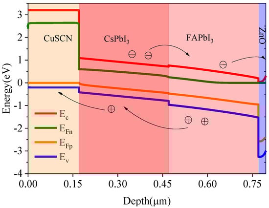
Figure 5.
Energy band of the device (the thicknesses of CsPbI3 and FAPbI3 are both 300 nm).
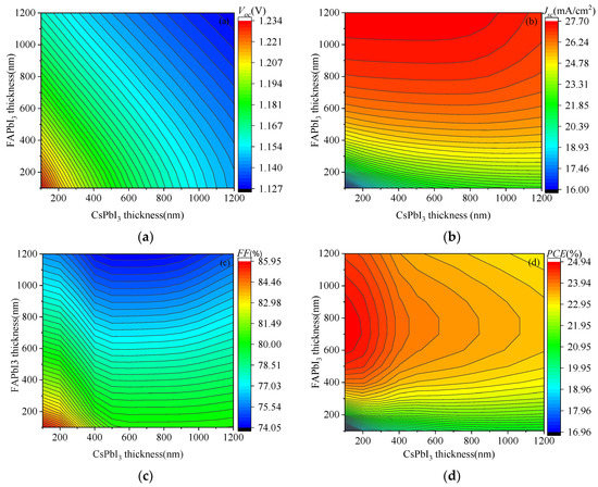
Figure 6.
Effect of the thickness of the photoactive layer on the output characteristics of the cell: (a) effect of the thickness on the open circuit voltage (Voc), (b) effect of the thickness on the short-circuit current density (Jsc), (c) effect of the thickness on the fill factor (FF), and (d) effect of the thickness on the power conversion efficiency (PCE).
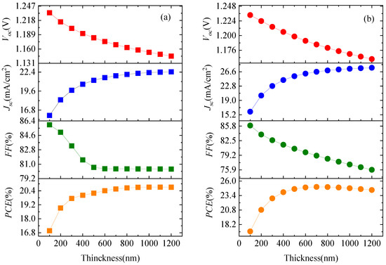
Figure 7.
Effects of the thicknesses of CsPbI3 and FAPbI3: (a) effects of the thickness of CsPbI3 (the thickness of FAPbI3 is fixed at 100 nm), (b) effects of the thickness of FAPbI3 (the thickness of CsPbI3 is fixed 100 nm).
QE measures the absorption of photons by the device. As the thickness of the photoactive layer increases, the photons absorbed by the device improves, and the QE shows a rising trend (as shown in Figure 8), which leads to an increase in the photogenerated carrier concentration [19]. As a result, Jsc gradually increases. Figure 6b shows that as the thickness increases from 100 to 1200 nm, the thickness change of the FAPbI3 had a more significant effect on Jsc than that of the CsPbI3. The thickness change of the FAPbI3 makes the trend of the change in QE of the device more significant, resulting in a larger difference in the photon absorption effect. This means that the thickness change of the FAPbI3 has a more significant effect on Jsc compared with that of CsPbI3.
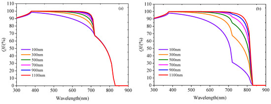
Figure 8.
Effect of thickness changes on the quantum efficiency (QE): (a) effect of the CsPbI3 thickness on the QE and (b) effect of the FAPbI3 thickness on the QE.
The following equation describes the inverse relationship between Voc and the diode reverse saturation current J0 [44]:
where k is the Boltzmann constant, T is the temperature, Jl is the photo-generated current.
As the thicknesses of the CsPbI3 and FAPbI3 increase, the carrier diffusion length increases, and the recombination rate of carriers rises as well, so Voc gradually reduces. In addition, an increase in the thickness of the photoactive layer would lead to the increase in the series resistance of the device, as well as the internal power consumption [44]. As a result, the FF performance tends to decrease. According to the analysis of Figure 6d, when the thicknesses of CsPbI3 and FAPbI3 are 100 and 700 nm, respectively, the cell achieves the highest PCE.
The effect of the defect density Nt of the photoactive layers of CsPbI3 and FAPbI3 on the J-V characteristics of the cells are shown in Figure 9a,b, respectively. As the value of Nt of the photoactive layer increases from 1012 to 1018 cm−3, the J-V characteristics of the cell gradually deteriorate, the PCE goes down (see Figure 10), and the cell performance gradually declines. Increasing Nt in the photoactive layer is equivalent to introducing more carrier recombination centers inside the cell [19]. This would cause the carrier recombination rate to increase (the simulation results are shown in Figure 11), the carrier diffusion length to be shorter, and the carrier lifetime to shrink [46]. The minority carrier lifetime τ and the carrier diffusion length LD can be obtained using Equations (13) and (14) [11]:
where μ(e,h) is the mobility of electrons and holes, δ is the trapping cross-sectional area of electrons and holes, and νth is the thermal velocity of the carrier.
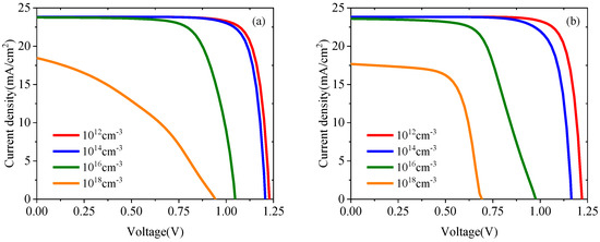
Figure 9.
Effect of the defect density of the photoactive layer on cell performance: (a) effect of the defect density of the CsPbI3 on the cell’s J-V characteristics and (b) effect of the defect density of the FAPbI3 on the cell’s J-V characteristics.
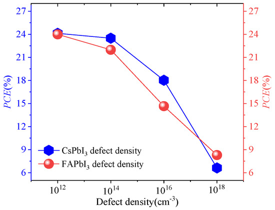
Figure 10.
PCE as a function of the defect density of the photoactive layer.
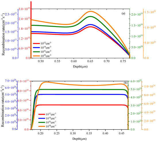
Figure 11.
Carrier recombination rates for different defect densities of the photoactive (a) CsPbI3 and (b) FAPbI3 layers.
Equations (13) and (14) indicate that with increasing Nt, τ decreases gradually. As a result, both LD and Voc decrease gradually. Therefore, to achieve a better cell performance, the Nt value of the photoactive layer should be controlled within a relatively low range. Considering the difficulty of preparing thin films with a low defect density in the actual preparation process, 1012 cm−3 is set as the optimal Nt value for the two photoactive layers of CsPbI3 and FAPbI3 based on the simulation results.
3.2. Effect of Work Function of Metal Back Electrode on Cell Performance
For the output performance of the cell, the work function фb of the metal back electrode is also a key parameter. The value of фb has a direct impact on whether the cell has a suitable built-in electric field [38], and the size of the built-in electric field is related to the transport and collection of holes, so фb plays a crucial role in Voc [47]. To analyze the impact of back electrodes with different фb values on the cell performance, фb is set in the range of 4.5–5.1 eV in this study, and the simulation results are shown in Figure 12. Figure 12a shows that for this structure, when фb gradually increases from 4.5 eV, the device output Voc gradually becomes larger, and the J-V effect is improved. However, when фb is greater than 4.8 eV, the J-V characteristic curves of the device generally overlap with each other. Similarly, it can be seen from Figure 12b that when фb gradually increases from 4.5 to 4.8 eV, the PCE exhibits a gradual increase, and when фb is greater than 4.8 eV, the PCE has a minor difference.
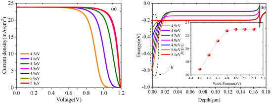
Figure 12.
Effects of the metal back electrode with different work functions on the cells: (a) J-V characteristics of back electrode cells with different work functions and (b) energy band differences of back electrode cells with different work functions.
When фb is less than 4.8 eV, the cell performance is apparently inhibited. A possible reason for this is the formation of Schottky junctions at the interface of CuSCN and the back electrode [48,49], as shown by the dashed line in Figure 12b. As фb decreases, the Schottky barrier gradually increases, the holes would need more energy to cross the Schottky barrier, and the transport process of holes to the back electrode is hindered [38], which inhibits the effective collection of holes. Therefore, Voc gradually decreases, which further limits the output of the PCE.
By using a back electrode with a high work function, the Fermi level is lowered, which could facilitate the production of better ohmic contacts [50]. Therefore, to prepare high-efficiency PSCs, it is very important to choose a suitable back contact material. The HTL and the back electrode should form an ohmic contact at the interface as much as possible to avoid the formation of an excessively high Schottky barrier. For the structure in this study, the back-electrode material should be chosen with фb greater than 4.8 eV.
3.3. Effect of Work Function of Front Electrode on Cell Performance
Similarly, the work function фf of the front electrode of the device has a direct correlation to the transport and collection of electrons, and thus, it affects the cell performance. During the preparation of PSCs, FTO or tin-doped indium oxide (ITO) is generally used as the front electrode. Previous studies [50,51] confirmed that the фf of ITO can be adjusted experimentally in the range of 4.6–5.0 eV. To compare with FTO (whose work function is 4.4 eV), in this study, ITO is set as the front electrode and фf is set in the range of 4.6–5.0 eV. The simulation results are shown in Figure 13: as фf increases, Voc slowly decreases, the J-V characteristics deteriorate, and the PCE declines as well.
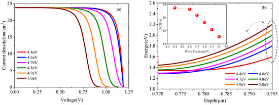
Figure 13.
Effects of the front electrodes with different work functions on the cell: (a) J-V characteristics of the front electrodes with different work functions and (b) energy band differences of the front electrodes with different work functions.
When фf gradually increases, a potential barrier is formed at the interface between the ZnO and the front electrode slowly becomes larger, as shown by the dashed line in Figure 13b. The process of electrons being transported to the front electrode and efficiently collected requires more energy. Thus, the electron transport is hindered, and Voc gradually decreases, which led to decreasing PCE. This comparison shows that for this device, when FTO with a фf value of 4.4 eV is selected as the front electrode, a potential barrier would be formed at the interface between ZnO and the front electrode reaches the lowest point, the J-V characteristics are good, and the cell achieves its highest PCE.
3.4. Effect of Working Temperature on Cell Performance
PSCs generally work in an outdoor environment with a temperature exceeding 300 K [52], and the outdoor temperature has a direct impact on the cell performance. Therefore, in this study, the temperature T is set in the range of 300–500 K to explore the effect of the temperature on the cell performance. The experimental results are plotted in Figure 14. As T increases, Jsc remains essentially unchanged, but the cell output Voc gradually decreases, the J-V characteristics deteriorate, and the gradual decrease in Voc also leads to a decreasing trend of the PCE. Therefore, the change in T affects the output of the cell performance via its influence over Voc. The relationship between Voc and T can be described as follows [44]:
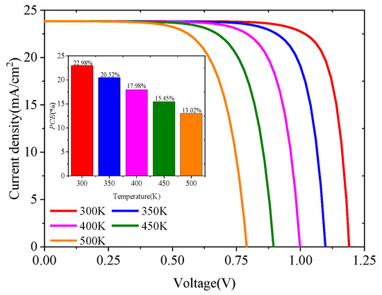
Figure 14.
Effect of the temperature on the cell performance.
It can be seen from Equation (15) that Voc and T have an inverse relationship. The increase in T causes Voc to decrease and promotes the increase in the diode reverse saturation current [53].
At high temperatures, electrons gain more energy, leading to their enhanced recombination with holes before being collected by the electrode [52]. Figure 15 confirms the inverse relationship between T and the carrier recombination rate, and therefore, an increase in T causes the overall performance of the cell to decline.
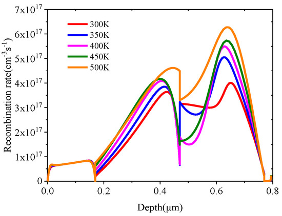
Figure 15.
Recombination rates of carriers at different operating temperatures.
Furthermore, as Voc decreases, the PCE also decreases. When T is excessively high, properties such as electron–hole mobility, carrier concentration, and band gap are all affected, resulting in a lower PCE output from the cell [54,55]. In summary, T and PCE have a linear relationship, and an increase in T will lead to a decrease in PCE. To provide cell outputs with better characteristics, the cells should avoid working in an environment with excessively high temperatures.
Based on the above discussion, for the cell device with the structure of FTO/ZnO/CsPbI3/FAPbI3/CuSCN/Au, the thicknesses of CsPbI3 and FAPbI3 are optimized to 100 and 700 nm, respectively. The defect densities of CsPbI3 and FAPbI3 are both set to 1012 cm−3, and the PCE reaches 28.75%. The J-V characteristic curves before and after optimization are plotted in Figure 16. Voc, Jsc, and PCE are increased by 17%, 9.5%, and 25.1%, respectively, and the cell performance after optimization improves as well.
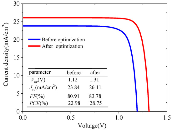
Figure 16.
Comparison of the cell performances before and after optimization.
Table 3 summarizes the results of recently published experimental and simulation studies on perovskite/perovskite bilayer heterojunction solar cells [5,14,17,19,20,39,56,57,58,59,60,61,62]. Since numerical simulations are carried out in ideal conditions, the simulation results are better than those obtained from experiments. The devices reported by Hu et al. [58] and Farhadi et al. [59] achieved more than 30% PCE, but both devices adopted TiO2 as the ETL and Farhadi et al. [59] used spiro-OMeTAD as the HTL, which is not conducive to device stability and would increase the preparation cost. On comparing the published data with the results of the present work, the proposed device model achieves a high efficiency of 28.75%. Moreover, the proposed model uses ZnO and CuSCN as its ETL and THL, respectively, which is helpful to improve device stability and reduce fabrication cost.
Table 3.
Comparing our results with those obtained from previous experimental and computational studies.
4. Conclusions
In this study, the SCAPS software was employed to explore the performance of PSCs with the structure of FTO/ZnO/CsPbI3/FAPbI3/CuSCN/Au. Currently there are few reports focusing on PSCs of this heterojunction structure. The simulation results obtained from the present study reveal that when ZnO and CuSCN are used as the ETL and HTL, respectively, the unstable performances of cell devices constructed by TiO2 and spiro-OMeTAD and the high costs could be effectively avoided. The combination of CsPbI3 and FAPbI3 for the heterojunction structure design could effectively broaden the absorption spectrum of the cell and promote a high Jsc cell output, thus, improving the PCE. When the thicknesses of CsPbI3 and FAPbI3 are 100 and 700 nm, respectively, the photon absorption is sufficient without a high recombination rate, and the cell reaches its highest PCE. When the defect densities of CsPbI3 and FAPbI3 are both 1012 cm−3, excessive carrier recombination centers inside the cell could be effectively avoided and the carrier lifetime could be extended. When the work function of the metal back electrode is greater than 4.8 eV and an FTO with a work function of 4.4 eV is selected as the front electrode, the excessive Schottky barrier could be avoided, and more ohmic contacts would be formed, promoting the collection of photogenerated carriers. A high operating temperature would cause the carrier recombination rate to increase, which inhibits the output of Voc. By optimizing the cell structure, the PCE reaches 28.75%, and the Voc, Jsc, and PCE are increased by 17%, 9.5%, and 25.1%, respectively. The simulation results present in this paper will help to further understand PSCs and improve the performances of heterojunction PSCs, therefore promoting the application of solar power as a form of clean and renewable energy along with wave energy [63,64] and wind energy [65,66].
Author Contributions
Y.G. and X.B. conceived of the presented idea, they developed the device structure and carried out the numerical analysis. D.Z. and B.Q. investigated the effects of absorber layer on cell performance; W.N. and R.Y. investigated the effects of contact electrodes on cell performance; and Q.J. studied the effects of working temperature on cell performance; Y.L. conducted the literature review and supervised the findings of this work. All authors contributed to the final version of the manuscript. All authors have read and agreed to the published version of the manuscript.
Funding
This research was funded by Guangxi Natural Science Foundation-Youth Fund Program (2021GXNSFBA220056), the high-quality talents research startup fund from the Yulin Normal University (G2019ZK24), Guangxi Key Laboratory of optoelectronic information processing project (GD21101), Guangxi University Young and Middle-aged Teachers’ Basic Scientific Research Ability Improvement Project (2022KY0580), China Foreign Expert Program (G2021033004L), Yulin Municipal School Cooperative Scientific Research Project (YLSXZD2019015).
Acknowledgments
The authors are grateful to Marc Bergelman from the University of Gent for providing the SCAPS simulation program.
Conflicts of Interest
The authors declare no conflict of interest. The funders had no role in the design of the study; in the collection, analyses, or interpretation of data; in the writing of the manuscript, or in the decision to publish the results.
References
- Shaikh, S.F.; Kwon, H.C.; Yang, W.; Mane, R.S.; Moon, J. Performance enhancement of mesoporous TiO2-based perovskite solar cells by ZnS ultrathin-interfacial modification layer. J. Alloys Compd. 2018, 738, 405–414. [Google Scholar] [CrossRef]
- Eperon, G.E.; Burlakov, V.M.; Docampo, P.; Goriely, A.; Snaith, H.J. Morphological control for high performance, solution-processed planar heterojunction perovskite solar cells. Adv. Funct. Mater. 2014, 24, 151–157. [Google Scholar] [CrossRef]
- Liu, M.; Johnston, M.B.; Snaith, H.J. Efficient planar heterojunction perovskite solar cells by vapour deposition. Nature 2013, 501, 395–398. [Google Scholar] [CrossRef]
- Min, H.; Lee, D.Y.; Kim, J.; Kim, G.; Lee, K.S.; Kim, J.; II Seok, S. Perovskite solar cells with atomically coherent interlayers on SnO2 electrodes. Nature 2021, 598, 444–450. [Google Scholar] [CrossRef]
- Mehrabian, M.; Norouzi, A.E.; Norouzzadeh, P. Numerical simulation of bilayer perovskite quantum dot solar cell with 18.55% efficiency. Opt. Quant. Electron. 2022, 54, 439. [Google Scholar] [CrossRef]
- Niu, T.; Chao, L.; Dong, X.; Li, F.; Chen, Y. Phase-pure α-FAPbI3 for perovskite solar cells. J. Phys. Chem. Lett. 2022, 13, 1845–1854. [Google Scholar] [CrossRef] [PubMed]
- Mari-Guaita, J.; Bouich, A.; Mari, B. Shedding light on phase stability and surface engineering of formamidinium lead Iodide (FaPbI3) thin films for solar cells. Eng. Proc. 2021, 12, 1. [Google Scholar] [CrossRef]
- Frolova, L.A.; Anokhin, D.V.; Piryazev, A.A.; Luchkin, S.Y.; Dremova, N.N.; Stevenson, K.J.; Troshin, P.A. Highly efficient all-inorganic planar heterojunction perovskite solar cells produced by thermal coevaporation of CsI and PbI2. J. Phys. Chem. Lett. 2017, 8, 67–72. [Google Scholar] [CrossRef]
- Bouich, A.; Mari-Guaita, J.; Baig, F.; Khattak, Y.H.; Soucase, B.M.; Palacios, P. Investigation of the surface coating, humidity degradation, and recovery of perovskite film phase for solar-cell applications. Nanomaterials 2022, 12, 3027. [Google Scholar] [CrossRef]
- Kim, Y.S.; Ri, C.H.; Ko, U.H.; Kye, Y.H.; Jong, U.G.; Yu, C.J. Interfacial enhancement of photovoltaic performance in MAPbI3/CsPbI3 superlattice. ACS Appl. Mater. Interfaces 2021, 13, 14679–14687. [Google Scholar] [CrossRef]
- Lin, L.; Jiang, L.; Li, P.; Xiong, H.; Kang, Z.; Fan, B.; Qiu, Y. Simulated development and optimized performance of CsPbI3 based all-inorganic perovskite solar cells. Sol. Energy 2020, 198, 454–460. [Google Scholar] [CrossRef]
- Chen, R.; Hui, Y.; Wu, B.; Wang, Y.; Huang, X.; Xu, Z.; Ruan, P.; Zhang, W.; Cheng, F.; Zhang, W.; et al. Moisture-tolerant and high-quality α-CsPbI3 films for efficient and table perovskite solar modules. J. Mater. Chem. A 2020, 8, 9597–9606. [Google Scholar] [CrossRef]
- Tai, E.G.; Wang, R.T.; Chen, J.Y.; Xu, G. A water-stable organic-inorganic hybrid perovskite for solar cells by inorganic passivation. Crystals 2019, 9, 83. [Google Scholar] [CrossRef]
- Li, F.; Zhou, S.; Yuan, J.; Qin, C.; Yang, Y.; Shi, J.; Ma, W. Perovskite quantum dot solar cells with 15.6% efficiency and improved stability enabled by an α-CsPbI3/FAPbI3 bilayer structure. ACS Energy Lett. 2019, 4, 2571–2578. [Google Scholar] [CrossRef]
- Zhou, Y.; Zhao, Y. Chemical stability and instability of inorganic halide perovskites. Energy Environ. Sci. 2019, 12, 1495–1511. [Google Scholar] [CrossRef]
- Li, C.; Wang, Y.; Choy, W.C.H. Efficient interconnection in perovskite tandem solar cells. Small Methods 2020, 4, 2000093. [Google Scholar] [CrossRef]
- Lin, L.; Jiang, L.; Li, P.; Chen, D.; Huang, S.; Xiong, H.; Sun, W.-H.; Qin, Y. Numerical simulation of novel designed HTL-free perovskite solar cells to realize over 25% efficiency based on CH3NH3PbI3/CH3NH3PbI2Br cascade structure. Opt. Mater. 2022, 129, 112496. [Google Scholar] [CrossRef]
- Akhtarianfar, S.F.; Shojaei, S.; Asl, S.K. High-performance CsPbI3/XPbI3 (X= MA and FA) heterojunction perovskite solar cell. Opt. Commun. 2022, 512, 128053. [Google Scholar] [CrossRef]
- Duan, Q.; Ji, J.; Hong, X.; Fu, Y.; Wang, C.; Zhou, K.; Wang, Z.-Y. Design of hole-transport-material free CH3NH3PbI3/CsSnI3 all-perovskite heterojunction efficient solar cells by device simulation. Sol. Energy 2020, 201, 555–560. [Google Scholar] [CrossRef]
- Xu, X.; Wang, J.; Cao, D.; Zhou, Y.; Jiao, Z. Design of all-inorganic hole-transport-material-free CsPbI3/CsSnI3 heterojunction solar cells by device simulation. Mater. Res. Express 2022, 9, 025509. [Google Scholar] [CrossRef]
- Clark, C.P.; Mann, J.E.; Bangsund, J.S.; Hsu, W.J.; Aydil, E.S.; Holmes, R.J. Formation of Stable Metal Halide Perovskite/Perovskite Heterojunctions. ACS Energy Lett. 2020, 5, 3443–3451. [Google Scholar] [CrossRef]
- Yang, T.C.J.; Fiala, P.; Jeangros, Q.; Ballif, C. High-bandgap perovskite materials for multijunction solar cells. Joule 2018, 2, 1421–1436. [Google Scholar] [CrossRef]
- Zhang, P.; Wu, J.; Zhang, T.; Wang, Y.; Liu, D.; Chen, H.; Li, S. Perovskite solar cells with ZnO electron-transporting materials. Adv. Mater. 2018, 30, 1703737. [Google Scholar] [CrossRef]
- Son, D.Y.; Im, J.H.; Kim, H.S.; Park, N.G. 11% efficient perovskite solar cell based on ZnO nanorods: An effective charge collection system. J. Phys. Chem. C 2014, 118, 16567–16573. [Google Scholar] [CrossRef]
- Tseng, Z.L.; Chiang, C.H.; Wu, C.G. Surface engineering of ZnO thin film for high efficiency planar perovskite solar cells. Sci. Rep. 2015, 5, 13211. [Google Scholar] [CrossRef]
- Liu, G.; Zhong, Y.; Mao, H.; Yang, J.; Dai, R.; Hu, X.; Chen, Y. Highly efficient and stable ZnO-based MA-free perovskite solar cells via overcoming interfacial mismatch and deprotonation reaction. Chem. Eng. J. 2022, 431, 134235. [Google Scholar] [CrossRef]
- Wu, X.; Zhang, J.; Qin, M.; Liu, K.; Lv, Z.; Qin, Z.; Lu, X. ZnO electron transporting layer engineering realized over 20% efficiency and over 1.28 V open-circuit voltage in all-inorganic perovskite solar cells. EcoMat 2022, 4, e12192. [Google Scholar] [CrossRef]
- Azri, F.; Meftah, A.; Sengouga, N.; Meftah, A. Electron and hole transport layers optimization by numerical simulation of a perovskite solar cell. Sol. Energy 2019, 181, 372–378. [Google Scholar] [CrossRef]
- Madhavan, V.E.; Zimmermann, I.; Baloch, A.A.; Manekkathodi, A.; Belaidi, A.; Tabet, N.; Nazeeruddin, M.K. CuSCN as hole transport material with 3D/2D perovskite solar cells. ACS Appl. Energy Mater. 2019, 3, 114–121. [Google Scholar] [CrossRef]
- Murugadoss, G.; Thangamuthu, R.; Kumar, S.M.S.; Anandhan, N.; Kumar, M.R.; Rathishkumar, A. Synthesis of ligand-free, large scale with high quality all-inorganic CsPbI3 and CsPb2Br5 nanocrystals and fabrication of all-inorganic perovskite solar cells. J. Alloys Compd. 2019, 787, 17–26. [Google Scholar] [CrossRef]
- Burgelman, M.; Nollet, P.; Degrave, S. Modelling polycrystalline semiconductor solar cells. Thin Solid Film. 2000, 361, 527–532. [Google Scholar] [CrossRef]
- Patel, P.K. Device simulation of highly efficient eco-friendly CH3NH3SnI3 perovskite solar cell. Sci. Rep. 2021, 11, 3082. [Google Scholar] [CrossRef]
- Mohanty, I.; Mangal, S.; Singh, U.P. Performance optimization of lead free-MASnI3/CIGS heterojunction solar cell with 28.7% efficiency: A numerical approach. Opt. Mater. 2021, 122, 111812. [Google Scholar] [CrossRef]
- Minemoto, T.; Matsui, T.; Takakura, H.; Hamakawa, Y.; Negami, T.; Hashimoto, Y.; Kitagawa, M. Theoretical analysis of the effect of conduction band offset of window/CIS layers on performance of CIS solar cells using device simulation. Sol. Energy Mater. Sol. Cells 2001, 67, 83–88. [Google Scholar] [CrossRef]
- Minemoto, T.; Hashimoto, Y.; Shams-Kolahi, W.; Satoh, T.; Negami, T.; Takakura, H.; Hamakawa, Y. Control of conduction band offset in wide-gap Cu(In, Ga)Se2 solar cells. Sol. Energy Mater. Sol. Cells 2003, 75, 121–126. [Google Scholar] [CrossRef]
- Minemoto, T.; Murata, M. Theoretical analysis on effect of band offsets in perovskite solar cells. Sol. Energy Mater. Sol. Cells 2015, 133, 8–14. [Google Scholar] [CrossRef]
- Lakhdar, N.; Hima, A. Electron transport material effect on performance of perovskite solar cells based on CH3NH3GeI3. Opt. Mater. 2020, 99, 109517. [Google Scholar] [CrossRef]
- Lin, L.; Jiang, L.; Li, P.; Fan, B.; Qiu, Y. A modeled perovskite solar cell structure with a Cu2O hole-transporting layer enabling over 20% efficiency by low-cost low-temperature processing. J. Phys. Chem. Solids 2019, 124, 205–211. [Google Scholar] [CrossRef]
- Karthick, S.; Velumani, S.; Bouclé, J. Experimental and SCAPS simulated formamidinium perovskite solar cells: A comparison of device performance. Sol. Energy 2020, 205, 349–357. [Google Scholar] [CrossRef]
- Gan, Y.; Bi, X.; Liu, Y.-C.; Qin, B.; Li, Q.; Jiang, Q.; Mo, P. Numerical investigation energy conversion performance of tin-based perovskite solar cells using cell capacitance simulator. Energies 2020, 13, 5907. [Google Scholar] [CrossRef]
- Yang, I.S.; Lee, S.; Choi, J.; Jung, M.T.; Kim, J.; Lee, W.I. Enhancement of open circuit voltage for CuSCN-based perovskite solar cells by controlling the perovskite/CuSCN interface with functional molecules. J. Mater. Chem. A 2019, 7, 6028–6037. [Google Scholar] [CrossRef]
- Hassan, A.; Wang, Z.; Ahn, Y.H.; Azam, M.; Khan, A.A.; Farooq, U.; Zubair, M.; Cao, Y. Recent defect passivation drifts and role of additive engineering in perovskite photovoltaics. Nano Energy 2022, 101, 107579. [Google Scholar] [CrossRef]
- Tan, K.; Lin, P.; Wang, G.; Liu, Y.; Xu, Z.; Lin, Y. Controllable design of solid-state perovskite solar cells by SCAPS device simulation. Solid-State Electron. 2016, 126, 75–80. [Google Scholar] [CrossRef]
- Devi, N.; Parrey, K.A.; Aziz, A.; Datta, S. Numerical simulations of perovskite thin-film solar cells using a CdS hole blocking layer. J. Vac. Sci. Technol. B 2018, 36, 04G105. [Google Scholar] [CrossRef]
- Liu, F.; Zhu, J.; Wei, J.; Li, Y.; Lv, M.; Yang, S.; Dai, S. Numerical simulation: Toward the design of high-efficiency planar perovskite solar cells. Appl. Phys. Lett. 2014, 104, 253508. [Google Scholar] [CrossRef]
- Sengar, B.S.; Garg, V.; Kumar, A.; Dwivedi, P. Numerical simulation: Design of high-efficiency planar pn homojunction perovskite solar cells. IEEE Trans. Electron Devices 2021, 68, 2360–2364. [Google Scholar] [CrossRef]
- Qiu, D.; Kim, E.K. Electrically tunable and negative Schottky barriers in multi-layered graphene/MoS2 heterostructured transistors. Sci. Rep. 2015, 5, 13743. [Google Scholar] [CrossRef]
- Lin, L.Y.; Jiang, L.Q.; Qiu, Y.; Fan, B.D. Analysis of Sb2Se3/CdS based photovoltaic cell: A numerical simulation approach. J. Phys. Chem. Solids 2018, 122, 19–24. [Google Scholar] [CrossRef]
- Gao, J.; Luther, J.M.; Semonin, O.E.; Ellingson, R.J.; Nozik, A.J.; Beard, M.C. Quantum dot size dependent J−V characteristics in heterojunction ZnO/PbS quantum dot solar cells. Nano Lett. 2011, 11, 1002–1008. [Google Scholar] [CrossRef]
- Shewchun, J.; Dubow, J.; Wilmsen, C.W.; Singh, R.; Burk, D.; Wager, J.F. The operation of the semiconductor-insulator-semiconductor solar cell: Experiment. J. Appl. Phys. 1979, 50, 2832–2839. [Google Scholar] [CrossRef]
- Park, Y.; Choong, V.; Gao, Y.; Hsieh, B.R.; Tang, C.W. Work function of indium tin oxide transparent conductor measured by photoelectron spectroscopy. Appl. Phys. Lett. 1996, 68, 2699–2701. [Google Scholar] [CrossRef]
- Karimi, E.; Ghorashi, S.M.B. Simulation of perovskite solar cell with P3HT hole-transporting materials. J. Nanophotonics 2017, 11, 032510. [Google Scholar] [CrossRef]
- Chakraborty, K.; Choudhury, M.G.; Paul, S. Numerical study of Cs2TiX6 (X = Br−, I−, F− and Cl−) based perovskite solar cell using SCAPS-1D device simulation. Sol. Energy 2019, 194, 886–892. [Google Scholar] [CrossRef]
- Nakada, T.; Mizutani, M. 18% efficiency Cd-free Cu(In, Ga)Se2 thin-film solar cells fabricated using chemical bath deposition (CBD)-ZnS buffer layers. Jpn. J. Appl. Phys. 2002, 41, L165. [Google Scholar] [CrossRef]
- Chelvanathan, P.; Hossain, M.I.; Amin, N. Performance analysis of copper–indium–gallium–diselenide (CIGS) solar cells with various buffer layers by SCAPS. Curr. Appl. Phys. 2010, 10, S387–S391. [Google Scholar] [CrossRef]
- Zhao, Q.; Hazarika, A.; Chen, X.; Harvey, S.P.; Larson, B.W.; Teeter, G.R.; Liu, J.; Song, T.; Xiao, C.; Shaw, L.; et al. High efficiency perovskite quantum dot solar cells with charge separating heterostructure. Nat. Commun. 2019, 10, 2842. [Google Scholar] [CrossRef] [PubMed]
- Hu, Y.; Schlipf, J.; Wussler, M.; Petrus, M.L.; Jaegermann, W.; Bein, T.; Muller-Buschbaum, P.; Docampo, P. Hybrid perovskite/perovskite heterojunction solar cells. ACS Nano 2016, 10, 5999–6007. [Google Scholar] [CrossRef] [PubMed]
- Farhadi, B.; Ciprian, M.; Zabihi, F.; Liu, A. Influence of contact electrode and light power on the efficiency of tandem perovskite solar cell: Numerical simulation. Sol. Energy 2021, 226, 161–172. [Google Scholar] [CrossRef]
- Abedini-Ahangarkola, H.; Soleimani-Amiri, S.; Rudi, S.G. Modeling and numerical simulation of high efficiency perovskite solar cell with three active layers. Sol. Energy 2022, 236, 724–732. [Google Scholar] [CrossRef]
- Mandadapu, U.; Vedanayakam, S.V.; Thyagarajan, K.; Babu, B.J. Optimisation of high efficiency tin halide perovskite solar cells using SCAPS-1D. Int. J. Simulat. Process Model. 2018, 13, 221. [Google Scholar] [CrossRef]
- Rai, S.; Pandey, B.K.; Dwivedi, D.K. Designing hole conductor free tin–lead halide based all-perovskite heterojunction solar cell by numerical simulation. J. Phys. Chem. Solids 2021, 156, 110168. [Google Scholar] [CrossRef]
- Baig, F.; Khattak, Y.H.; Marí, B.; Beg, S.; Ahmed, A.; Khan, K. Efficiency enhancement of CH3NH3SnI3 solar cells by device modeling. J. Electron. Mater. 2018, 47, 5275–5282. [Google Scholar] [CrossRef]
- Guiberteau, K.; Liu, Y.-C.; Lee, J.; Kozman, T.A. Investigation of developing wave energy technology in the Gulf of Mexico. Distrib. Gener. Altern. Energy J. 2012, 27, 36–52. [Google Scholar]
- Pastor, J.; Liu, Y.-C. Hydrokinetic energy: Overview and its renewable energy potential for the Gulf of Mexico. In Proceedings of the 2012 IEEE Green Technologies Conference, Tulsa, OK, USA, 19–20 April 2012; Institute of Electrical and Electronics Engineers (IEEE): Piscataway, NJ, USA, 2012; pp. 1–3. [Google Scholar]
- Chu, S.J.; Liu, Y.-C. Prospects of wind energy and wind power in Louisiana. In Proceedings of the 2011 IEEE Green Technologies Conference, Baton Rouge, LA, USA, 14–15 April 2011. [Google Scholar]
- Liu, Y.-C.; Chu, S.J. Advance application of wind technology in Louisiana. Int. J. Energy Eng. 2012, 2, 60–66. [Google Scholar] [CrossRef]


Publisher’s Note: MDPI stays neutral with regard to jurisdictional claims in published maps and institutional affiliations. |
© 2022 by the authors. Licensee MDPI, Basel, Switzerland. This article is an open access article distributed under the terms and conditions of the Creative Commons Attribution (CC BY) license (https://creativecommons.org/licenses/by/4.0/).