Article

Single-Stage Isolated and Bidirectional Three-Phase Series-Resonant AC–DC Converter: Modulation for Active and Reactive Power Control

1
GrEPO, CER-UNI, Universidad Nacional de Ingeniería, Lima 15333, Peru
2
G2Elab, CNRS, University Grenoble Alpes, F-38000 Grenoble, France
*
Authors to whom correspondence should be addressed.
Energies 2022, 15(21), 8070; https://doi.org/10.3390/en15218070
Submission received: 9 September 2022 / Revised: 1 October 2022 / Accepted: 6 October 2022 / Published: 30 October 2022

Abstract

:
Single-stage isolated and bidirectional (SSIB) AC–DC converters have a high potential for future solid-state transformers and smart battery chargers due to their reduced volume and high efficiency. However, there is a research gap for SSIB reactive power injection. This article introduces an SSIB three-phase AC–DC converter composed of three low frequency rectifiers linked by tiny film capacitors with a quad-active-bridge series-resonant (QABSR) DC–DC. A novel QAB modulation is proposed to solve three issues: (1) Three DC inputs with high ripple compensation, (2) active–reactive power injection, and (3) minimization of high-frequency (HF) transformers currents. The rectified grid voltages were modulated by time-variant duty ratio (DR) angles. In contrast, the DC source was modulated by a fixed DR (FDR) angle along with a phase-shift angle which changes according to the grid current amplitude. A constant HF current amplitude with minimum value was obtained. It is shown that the HF current amplitude is increased for reactive power injection. Hence, the FDR angle was used to compensate for this increase. Active and reactive power control were validated in a 2 kW prototype. Compared with other structures, tiny DC-link capacitors and smaller L filters were used. Moreover, higher efficiency (96%) and smaller grid currents THDi (3%) were obtained.

1. Introduction

1.1. Motivation

Bidirectional and isolated AC–DC converters with active and reactive power capability play an essential role in electric vehicles’ smart battery chargers (SBC) [1,2], and future solid-state transformers (SST) [3,4,5] to improve grid reliability, particularly for grid voltage regulation [1,2]. Galvanic isolation is required between the bidirectional DC source and the grid to ensure safety and low leakage currents. For these applications, the typical structures are two or three stage AC–DC converters [6,7]. In the typical two-stage converter, a voltage source inverter (VSI) is DC-linked by electrolytic capacitors with a dual-active bridge (DAB) DC–DC converter [6]. The DC-link voltage and capacitance are chosen in such a way that the VSI controls the active and reactive power transfer with the grid, whereas the DAB DC–DC allows galvanic isolation and only controls the active power transfer [8]. However, a well-known drawback is that the multi-stage conversion decreases the converter efficiency. Besides that, the DC-link capacitors along with the L filter (to grid interface) have a large size and weight [9]. Therefore, the single-stage isolated and bidirectional (SSIB) three-phase AC–DC converter is a good solution for these applications due to their reduced volume and high efficiency [4,10]. Nonetheless, in these converters the active and reactive power transfer must be directly handled by the high frequency (HF) transformer since DC-link capacitors are not present [11,12,13,14,15,16,17,18,19,20,21,22,23]. Nevertheless, in the state-of-the-art review, it is observed that in most of them, only the active power transfer is considered to analyze the steady-state response of the HF transformers current; whereas, the reactive power injection analysis was not covered. In order to fill this research gap, this article introduces an SSIB three-phase AC–DC, based on the quad-active-bridge series-resonant (QABSR) converter. It is shown that the reactive power injection with a small power factor can considerably increase the HF transformer current if the modulation is not adequate. Hence, special attention is provided to the QABSR modulation for active and reactive power injection, minimizing the current in the HF transformers.

1.2. Literature Review

This article classifies the SSIB three-phase AC–DC converters found in the literature, based on the DAB structure, in three different approaches according to the galvanic isolation.
The first approach for SSIB three-phase AC–DC converters consist of using a single HF transformer [11,12,13,14,15,16,17,18,19,20,21,22,23]. In these converters, the grid voltages are directly modulated using bipolar voltage switches with a fixed switching frequency. Furthermore, only the converters proposed in [21,22,23] analyze the reactive power injection. However, none have analyzed the influence of reactive power injection in the HF current. Moreover, due to the use of bipolar voltage switches, special care must be taken in the switching strategy and protection [24].
The second approach for SSIB three-phase AC–DC converters is two HF transformers usage [25,26,27]. A three-phase unfolder bridge cascaded with two independent DABs [25], two DAB series-resonant (DABSR) [26], or a triple-active-bridge series-resonant [27] DC–DC converters are presented. However, none of these converters analyze the reactive power injection capability.
The third approach for SSIB three-phase AC–DC is to use a three-phase Y Δ HF transformer [28] or three HF transformers [29,30,31,32]. Bipolar voltage switches are used in [28,29,30]. In contrast, unipolar voltage switches are used in [31,32], as shown in Figure 1. Note that three low frequency (LF) rectifiers cascaded with three independent DC–DC DABs are presented in Figure 1a, and the power flow is controlled by time-variant phase shifts and switching frequency, [31]. Nevertheless, a wide switching frequency variation complicates the filter design and compliance with EMI regulations [33]. Conversely, in Figure 1b, a quad-active-bridge (QAB) AC–DC converter with a fixed switching frequency is presented [32]. In this converter a C N capacitor is used to add a DC offset V o F S in the neutral reference ( V o F S > grid voltage amplitude), where unipolar voltage switches with a time-variant phase-shift modulation are used. However, the drawback is that the DC-offset voltage control and the phase shift are challenging to implement. In fact, the authors do not explain how the modulation was implemented. Moreover, similar to previous approaches, none have analyzed the influence of reactive power injection in the HF current. Hence, more studies are required for this issue related to the QAB converter.
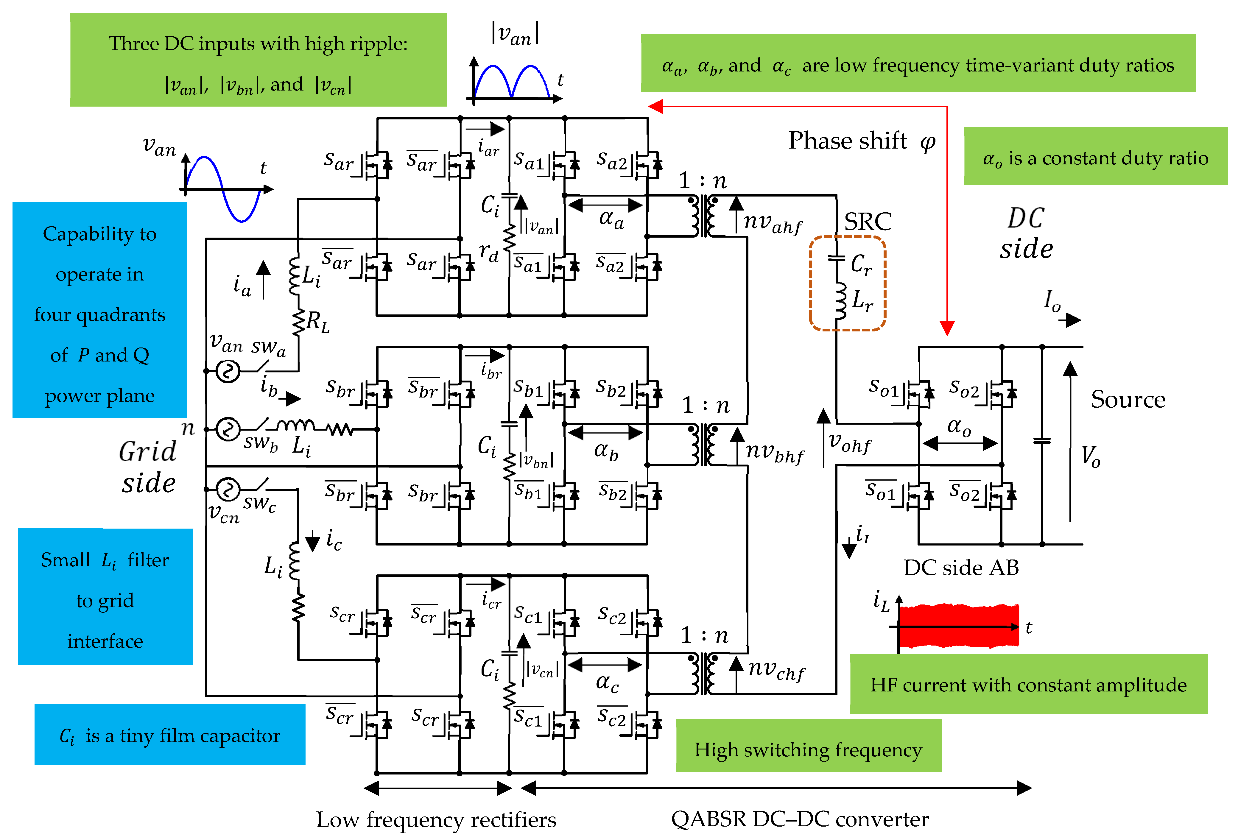
With these considerations, a novel SSIB three-phase AC–DC converter is proposed in this article, depicted in Figure 2. The proposed converter combines the structures shown in Figure 1 where the HF inductor L d is replaced by a series-resonant circuit (SRC). The converter is composed of three low frequency rectifiers linked, by tiny film capacitors, with a QABSR DC–DC. Therefore, the benefits of galvanic isolation, reduced volume, and high efficiency by Zero Voltage Switching (ZVS) turn-on and absence of turn-off voltage spikes are obtained. An important advantage is the absence of the big DC-link capacitors and reduced L filter to grid interface. However, because of the low frequency rectifiers and the tiny film DC-link capacitors (which do not allow the power decoupling), the proposed QABSR DC–DC modulation must offer the following functionalities: (1) compensation of the three DC inputs with high ripples (the rectified grid voltages), (2) active and reactive grid power injection, and (3) minimization of HF transformers current. With the aim of compensating for these three DC ripples and to minimize the HF current amplitude for active and reactive power injection, a novel QAB modulation is introduced. Due to the proposed modulation, a decoupled grid currents control in the natural frame is implemented, obtaining good performance even for unbalanced grid conditions. The proposed structure was introduced in [34] but with only simulation results and without reactive power analysis. In this article, experimental validation is carried out and reactive power compensation is introduced along with a more detailed analysis. It is shown that reactive power injection with a small power factor, can cause a considerable increase in the HF transformer current if the modulation is not adequate.

1.3. Contributions

The contributions of this paper are the following:
  • A novel SSIB three-phase AC–DC converter is proposed, which avoids bipolar voltage switches usage. The converter is composed of three LF rectifiers linked, by tiny film capacitors, with a QABSR DC–DC converter. Compared with similar SSIB AC–DC structures, a higher efficiency and smaller grid currents THD are obtained. Moreover, compared with a two-stage AC–DC converter, higher efficiency and smaller volume are obtained since tiny DC-link capacitances and smaller L filters to grid interface are used;
  • A novel duty ratio modulation is proposed to compensate for three DC inputs with high ripple (the rectified grid voltages) in the QABSR DC–DC converter. For this purpose, the rectified grid voltages are modulated by time-variant duty ratio modulation whose angles change according to the grid current angles. In contrast, the DC source is modulated by duty ratio and phase-shift modulation whose angles take a constant value, throughout the grid period, according to the grid current amplitude. The proposed modulation allows to obtain a HF current with constant amplitude and minimum value, throughout the grid period;
  • It is shown that, because of the single-stage AC–DC conversion (absence of the DC-link capacitors with high capacitance value), reactive power grid injection with a small power factor can considerably increase the current in HF transformers. Hence, a novel reactive power compensation using duty ratio modulation on the DC-side AB is introduced to minimize this increase;
  • The proposed QAB modulation allows to implement a decoupled closed-loop grid currents control in the natural frame, obtaining good performances even for unbalanced grid voltage conditions;
  • A practical methodology is introduced to easily size the proposed QABSR DC–DC as an equivalent DABSR DC–DC converter.

1.4. Organizations

This article is divided into the following sections: Section 2 introduces the converter, the modulation, the working principle of the HF three-phase power decoupling, the reactive power compensation, and the ZVS analysis. The closed-loop controller is explained in Section 3. The converter design is explained in Section 4. Experimental results are shown in Section 5. Afterward, Section 6 discusses unbalanced grid voltages conditions and compares the proposed converter with similar structures and with the typical two-stage AC–DC converter. Finally, conclusions are drawn and presented in Section 7.

2. The Proposed Converter

2.1. Structure Description

The proposed converter is shown in Figure 2. The three LF rectifiers and the QABSR DC–DC converter are linked by tiny capacitors C i . On the grid side, three L filters are used. The capacitor C i and the L filter are designed as a second-order low-pass filter with a damping resistor r d . The rectified grid voltages and the DC source are modulated by four active bridges (Abs). Three HF transformers with the same turns ratio n allow galvanic isolation and are series-connected on the secondary side where the SRC is placed.
Three features make the proposed converter different from the two-stage three-phase AC–DC converters where the QAB DC–DC converter is used [35,36,37,38,39]:
First, is the absence of the bulky DC-link capacitors for power decoupling. Indeed, in the proposed converter, the DC-link capacitors C i (see Figure 2) are sized to filter the HF current having a very small capacitance values, thus making it a single-stage AC–DC converter [31]. Hence, the three rectified grid voltages (which are DC voltages with high ripples) and the DC source are the QABSR DC inputs. In contrast, in the two-stage three-phase AC–DC converter, the DC-link capacitors have a larger capacitance value and the QAB has four DC inputs with a very small ripple [35,36,37,38,39,40,41,42,43,44,45,46,47].
Second, is the use of the three LF rectifiers (see Figure 2), which switch at zero crossing of each grid voltage. In this stage only conduction losses are considered, making the converter highly efficient. In contrast, in the two-stage three-phase AC–DC, the VSI stage, which can be two level [8] or multilevel [35,36,37,38,39], switches at HF. Hence, switching and conduction losses are considered in this stage. Then, in the proposed converter, the losses are decreased compared with a two-stage isolated AC–DC converter.
Third, is smaller L filter to grid interface. In the two-stage AC–DC converter, the L filter depends on the DC-link voltage value. The higher the DC-link voltage, the larger the L filter [48]. Hence, multilevel AC–DC converters were proposed to decrease the L filter volume for SST [34,35,36,37,38]. However, this solution requires to increase the H-bridge modules and the price can be considerably increased [49]. In contrast, in the proposed converter, the L filter is considerably smaller than a two-level VSI because of the absence of DC-link capacitors with high capacitance value.
However, due to the tiny capacitance C i , three functionalities must be offered for the proposed QABSR DC–DC converter: first, compensation of the three DC inputs with high ripple (the rectified grid voltages), second, to directly handle the active–reactive power transfer and third, to minimize the HF current. With the aim of solving these problems, a novel QAB modulation is introduced as is shown in the following section.

2.2. The Modulation

For this analysis, the grid voltages are defined as:
{ v a n = V m sin ( ω g t )   v b n = V m sin ( ω g t 2 π 3 ) v c n = V m sin ( ω g t + 2 π 3 )
where V m is the voltage amplitude and ω g is the grid frequency. Then, for active and reactive grid power injection, the balanced three-phase grid currents are provided by:
{   i a = I m sin ( ω g t θ )   i b = I m sin ( ω g t 2 π 3 θ ) i c = I m sin ( ω g t + 2 π 3 θ )
where I m is the grid current amplitude and θ is the displacement power factor angle (DPFA). Hence, the modulation for the three LF rectifiers is provided by:
s i r = s g n ( v i n ) ;   For   i = a ,   b ,   c
Being the function s g n ( x ) defined as:
s g n ( x ) = { 1 ;   w h e n   x 0 0 ;   w h e n   x < 0
According to Figure 2, the rectified grid currents i a r , i b r and i c r are provided by:
i a r = {   i a ,   w h e n   v a n 0 i a ,   w h e n   v a n < 0 ;   i b r = {   i b ,   w h e n   v b n 0 i b ,   w h e n   v b n < 0 ;   i c r = {   i c ,   w h e n   v c n 0 i c ,   w h e n   v c n < 0
where v a n , v b n , and v c n are the grid voltages defined in (1).
On the other hand, the rectified grid voltages | v a n | , | v b n | and | v c n | are the QABSR DC inputs (see Figure 2) which are modulated by the following function:
{ s a 1 = s g n ( c o s ( ω s t α a 2 ) ) s a 2 = s g n ( c o s ( ω s t + α a 2 ) ) ; { s b 1 = s g n ( c o s ( ω s t α b 2 ) ) s b 2 = s g n ( c o s ( ω s t + α b 2 ) )   ; { s c 1 = s g n ( c o s ( ω s t α c 2 ) ) s c 2 = s g n ( c o s ( ω s t + α c 2 ) )
While the DC source V o (see Figure 2) is modulated by the following function:
{ s o 1 = s g n ( cos ( ω s t α o 2 φ ) ) s o 2 = s g n ( cos ( ω s t + α o 2 φ ) )  
where ω s is the switching frequency, α a ,   α b ,   α c ,   α o are the DR angles, and φ is the PS angle. In the proposed modulation, α a ,   α b , and α c take the instantaneous values of the angle of rectified grid currents i a r ,   i b r , and i c r respectively, provided by (5), which means:
{ α a 2 = ω g t θ   α b 2 = ω g t 2 π 3 θ α c 2 = ω g t + 2 π 3 θ   ;   Where   ω g t     [ 0 ,   π ]
And the DR α o changes according to the DPFA θ , which means:
α o 2 = π 2 θ
The modulated voltages, evaluated at ω g t = π 2 , and the rectified grid currents, considering θ = 0 and θ = π 6 , are represented in Figure 3 and Figure 4, respectively.
In Figure 3 and Figure 4 the rectified grid voltages | v a n | ,   | v b n | ,   | v c n | are HF modulated by the DR angles: α a ,   α b , and α c , resulting in voltages v a h f , v b h f , and v c h f , respectively; whereas, the DC source V o is modulated by the DR α o along with a PS angle φ , resulting in voltage v o h f . In the proposed modulation, only one phase shift is used: φ , which allows to control the grid current amplitude, and then, the bidirectional power flow between the grid and the DC source V o .
Moreover, in Figure 3 and Figure 4 in grid period 2 π / ω g , the v a h f , v b h f , and v c h f amplitudes and the DR angles α a ,   α b , and α c are time-variant according to ( 1 ) and (8), respectively. Then, as shown in Figure 3c, for θ = 0 and ω g t = π 2 , the voltages v b h f and v c h f take the same instantaneous values (amplitude and DR), overlapping each other. Whereas in Figure 4c, for θ = π 6 and ω g t = π 2 , the DR α c = 0 , then v c h f = 0 , unlike v a h f and v b h f . In change, the amplitude V o , the DR α o , and the PS angle φ of v o h f take a constant value throughout the grid period. Moreover, in Figure 4c α o is reduced when the DPFA θ is increased, which allows to decrease the HF current when reactive power is injected into the grid. With the aim of clarifying the proposed modulation, the working principle of the QABSR DC–DC converter is explained in the following section.

2.3. Working Principle: The HF Three-Phase Power Decoupling

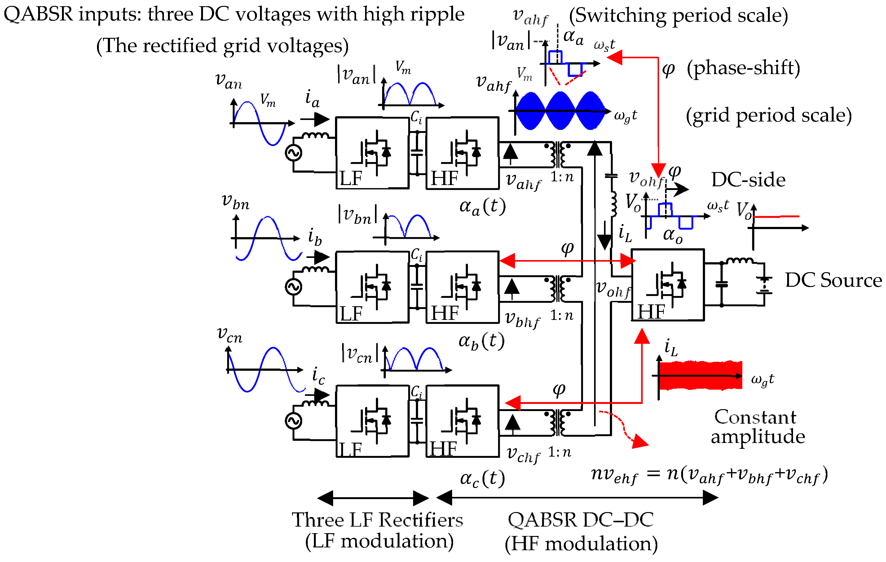
The working principle of the proposed converter is graphically presented in Figure 5. Note that two frequency modulations are employed: at LF by the three rectifiers and at HF by the QABSR DC–DC converter.
The three LF rectifiers switch at grid frequency, according to (3), resulting in the rectified voltages | v a n | ,   | v b n | , and | v c n | . The three LF rectifiers along with the three HF transformers are used to modulate the grid voltages independently. Note that in the LF rectifiers, MOSFETs are used to bidirectional power flow.
In the QABSR DC–DC converter, | v a n | ,   | v b n | , and | v c n | are HF modulated by their correspondent DR angles α a ,   α b , and α c , resulting in the modulated voltages v a h f , v b h f , and v c h f . The DR angles α a ,   α b , and α c are LF time-variant according to (8). This means, in grid period 2 π / ω g , the v a h f , v b h f , and v c h f amplitudes and the DR angles α a ,   α b , and α c are LF time-variant, as shown in Figure 4 for the case of v a h f ; whereas, in switching period 2 π / ω s , the v a h f , v b h f , and v c h f amplitudes and the DR angles α a ,   α b , and α c can be considered constants because the switching frequency ω s ω g (grid frequency), as shown in Figure 4 for the case of v a h f . In contrast, the DC source V o is modulated by the DR α o along with a PS angle φ , resulting in the modulated voltage v o h f . In the proposed modulation α o and φ take a constant value throughout the grid period unlike v a h f , v b h f , and v c h f . On the other hand, the three HF transformers have the same turns-ratio relationship n and are series-connected on the secondary side where the SRC is placed. Hence, the modulated voltages v a h f , v b h f , and v c h f are added on the HF transformer secondary side resulting in the voltage n v e h f = n ( v a h f + v b h f + v c h f ) , which is LF time-variant as v a h f , v b h f , and v c h f . Therefore, two different voltages are applied to the SRC: on the left side n v e h f , which is LF time-variant (in amplitude and DR); whereas, on the right side v o h f , which takes a constant value in amplitude, DR, and PS throughout the grid period. This means, the voltages applied to the SRC have different electrical features which can generate an overcurrent if the modulation is not adequate.
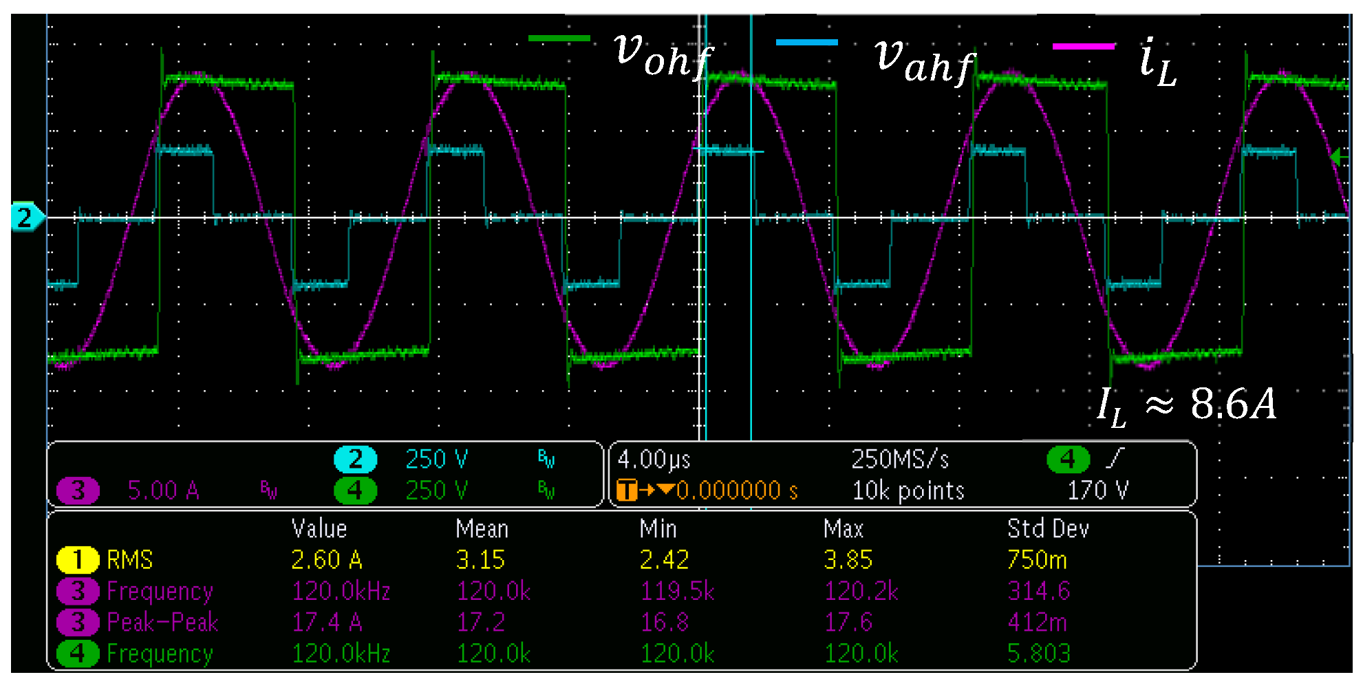
To overcome this issue, the proposed modulation takes advantage of the sum of modulated voltages n v e h f = n ( v a h f + v b h f + v c h f ) on the HF transformer secondary side. The main purpose is obtaining an equivalent voltage n v e h f which takes a constant value in amplitude and DR throughout the grid period similarly as v o h f . Hence, the resulting current in the HF transformer i L has a constant amplitude as shown in Figure 4.
With the previous considerations, in the proposed modulation, the voltages v a h f , v b h f , and v c h f are phase-shifted with respect to v o h f with the same angle φ as represented in Figure 4. In this way, the power flow can be controlled by the phase-shift angle φ ; whereas, the DRs angles α a ,   α b , and α c allow to compensate for the time voltage variations in n v e h f . These aspects are explained in the following.
Indeed, the modulated voltages v i h f ( for   i = a ,   b ,   c ) and v o h f can be expressed using Fourier series as:
v i h f = | v i n | × k = 1 , 3 4 k π cos ( k ( π 2 α i 2 ) ) sin ( k ( ω s t ) )   ;   For   i = a ,   b ,   c
v o h f = V o × k = 1 , 3 4 k π cos ( k ( π 2 α o 2 ) ) sin ( k ( ω s t φ ) )
where | v i n | and α i 2 , for   i = a ,   b ,   c , are the rectified voltages | v a n | ,   | v b n | , and | v c n | and the DR angles α a 2 ,   α b 2 , and α c 2 , respectively.
On the other hand, the SRC is designed to obtain a high selectivity at ω s . Hence, the equivalent SRC at steady state is shown in Figure 6. The voltages v a h f 1 ,   v b h f 1 , v c h f 1 , and v o h f 1 are the harmonics at ω s of the modulated voltages which, according to (10) and (11) are provided by:
v i h f 1 = 4 π V i h f 1 sin ( ω s t )
Being :   V i h f 1 = | v i n | sin ( α i 2 ) ;   For   i = a ,   b ,   c
And the voltage on the HF transformers secondary side is:
n v e q 1 = n ( v a h f 1 + v b h f 1 + v c h f 1 )
Hence, replacing (12) in (14):
n v e q 1 = 4 π n V e q 1 sin ( ω s t )
Being:
V e q 1 = | v a n | sin ( α a 2 ) + | v b n | sin ( α b 2 ) + | v c n | sin ( α c 2 )
Because the DR angles α a 2 , α b 2 and α c 2 take the instantaneous values of the rectified grid current angles provided by (8), the amplitude V e q 1 provided in (16) can be calculated as:
V e q 1 = V a h f 1 + V b h f 1 + V c h f 1
where:
{ V a h f 1 = V m 2 [ cos ( θ ) cos ( 2 ω g t θ ) ]   V b h f 1 = V m 2 [ cos ( θ ) cos ( 2 ω g t 4 π 3 θ ) ] V c h f 1 = V m 2 [ cos ( θ ) cos ( 2 ω g t + 4 π 3 θ ) ]  
V m is the grid voltage amplitude and θ is the displacement power factor angle provided in (1) and (2), respectively. Note in (18) that, V a h f 1 + V b h f 1 + V c h f 1 contains a balanced three-phase system which is provided by:
cos ( 2 ω g t θ ) + cos ( 2 ω g t 4 π 3 θ ) + cos ( 2 ω g t + 4 π 3 θ ) = 0
Then, replacing (19) in (17), the amplitude V e q 1 is provided by:
V e q 1 = [ 3 2 V m ] cos ( θ )
According to (20), the amplitude V e q 1 takes the constant value of 3 2 V m cos ( θ ) throughout the grid period. This steady-state behavior is called in this article “HF three-phase power decoupling”, because the similarity with the power of a balanced three-phase system.
On the other hand, according to (11), the modulated DC source v o h f 1 is:
v o h f 1 = 4 π V o 1 sin ( ω s t φ )
Being :   V o 1 = V o sin ( α o 2 )
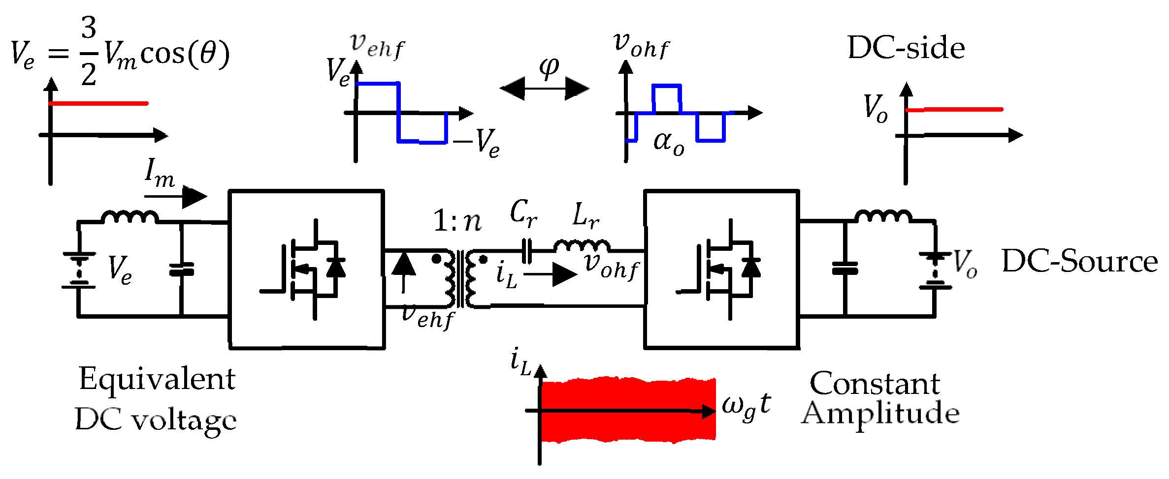
where the DR angle α o 2 and the PS angle φ take a constant value throughout the grid period. Because V e q 1 and V o have constant amplitude and DR, the HF current i L also has a constant amplitude throughout the grid period. Hence, the QABSR steady-state response is similar to that of a DABSR DC–DC converter [50,51] as shown in Figure 7, where HF current amplitude is controlled using the PS angle φ .
The turns ratio n is sized considering the maximum values of V o 1 and V e q 1 . Then, for only active power injection ( θ = 0 ) and for the DR angle α o 2 = π 2 , the SRC current can be minimized if the turns ratio n is designed to match the voltages in the equivalent SRC [51], which means:
n = V o 1 V e q 1 = V o 3 2 V m
Moreover, the tank circuit is designed as a band-pass filter at the switching frequency ω s . For this purpose, the quality factor Q is chosen with a high value ( Q 4 ), while the resonance frequency ω r is selected closest to ω s ( ω s 1.1   ω r ) [50,51]. These parameters are defined as:
Q = Z 8 π 2 R o   ;   ω r = 1 L r C r
Being:
Z = L r C r   ;   F = ω s ω r   ;   R o = V o 2 P o
where R o is the equivalent output load, V o is the DC output voltage, P o is the nominal power, F is the frequency ratio, and Z is the SRC impedance.
With these considerations, the resulting SRC current i L can be calculated as:
i L = 4 π n V e q 1 cos ( ω s t ) V o 1 cos ( ω s t φ ) Z ( F 1 F )
Being Z and F defined in (25). Thus, considering the SRC current provided by:
i L = I L sin ( ω s t σ )
The amplitude I L can be calculated with (26) as:
I L = 4 π Z ( F 1 F ) V o 1 2 + ( n V e q 1 ) 2 2 V o 1 ( n V e q 1 ) cos ( φ )
On the other hand, the average input current i a r for the QABSR, in one switching period, can be calculated as:
i a r = 1 2 π 0 2 π [ n i L × ( s a 1 s a 2 ) ]   d ( ω s t )
Being s a 1 , and s a 2 defined in (6), and n the turns ratio. A similar approach is applied to calculate i b r and i c r . Hence, solving (29), i a r ,   i b r , and i c r are calculated as:
{ i a r = [ K sin ( φ ) ] sin ( α a 2 ) i b r = [ K sin ( φ ) ] sin ( α b 2 ) i c r = [ K sin ( φ ) ] sin ( α c 2 )
Being:
K = K o sin ( α o 2 ) ;   And   K o = 8 n π 2 Z ( F 1 F ) V o
where sin ( α o 2 ) , provided by (22), takes a constant value throughout the grid period. Note in (30) that the PS angle φ is repeated in the three grid currents, while the DR angles are independents for each grid current. Thus, in the proposed control strategy, the PS angle φ is used to control the grid current amplitude, whereas the DR angles α a 2 , α b 2 and α c 2 are used to generate the rectified grid current angles provided by (8). Then, the angle φ is calculated as:
φ = a sin ( I m K )
where K is defined in (31) and I m is defined in (2). The DR angles α a 2 , α b 2 ,   α c 2 can be calculated comparing (5) and (2) with (30), thus:
α a 2 = asin ( i a r I m ) ;   α b 2 = asin ( i b r I m )   and   α c 2 = asin ( i c r I m )

2.4. Reactive Power Compensation by DR Modulation

According to (20), the voltage on the secondary side of the HF transformers n V e q 1 = n [ 3 2 V m ] cos ( θ ) , where θ is the grid displacement power factor angle, takes its maximum value when only active power P is injected ( cos ( θ ) = π 2 ) . However, V e q 1 is decreased when reactive power is injected which, according to (28), has a direct impact on the HF current amplitude I L . The critical case is when only reactive power is injected, which means, P = 0 , cos ( θ ) = 0 and V e q 1 = 0 . For this case, using (28), I L is provided by:
I L | θ = π 2 = 4 π Z ( F 1 F ) V o 1 = 4 π Z ( F 1 F ) V o sin ( α o 2 )
Note in (34) that the amplitude I L can be minimized using the DR angle α o 2 . This minimization must ensure a real solution in (32), which means K I m . Then, replacing (31) and (22) in (32), the minimum value of sin ( α o 2 ) is provided by:
sin ( α o 2 ) m i n = ( I m K o   sin ( φ ) )
where K o is provided by (31). According to (35), sin ( α o 2 ) m i n takes its minimum value at sin ( φ ) = 1 ,   ( i . e . ,   φ = π 2 ) , which allows to minimize the amplitude I L | θ = π 2 provided by (34). Hence, two methods are proposed to compensate for the voltage drop on the secondary side of the HF transformers n V e q 1 :
First Method: for cos ( θ ) 0.5 , the DR α o 2 is used to match the voltages applied to the tank circuit, which means V o sin ( α o 2 ) = n [ 3 2 V m ] cos ( θ ) , then:
α o 2 = π 2 θ ;   A n d   φ = a sin ( I m K o s i n ( α o 2 ) )
Second Method: for cos ( θ ) < 0.5
α o 2 = asin ( I m K o ) ;   And   φ = π 2
where K o is provided by (31). Note that for the first method, with the aim of obtaining a real solution, sin ( α o 2 ) I m K o . Hence, for θ π 2 , the DR α o 2 is limited to α o 2 = asin ( I m K o ) and φ = π 2 . This means, for these cases, both methods are equal. Both methods are analyzed in Section 5.

2.5. ZVS Analysis for the QABSR Converter

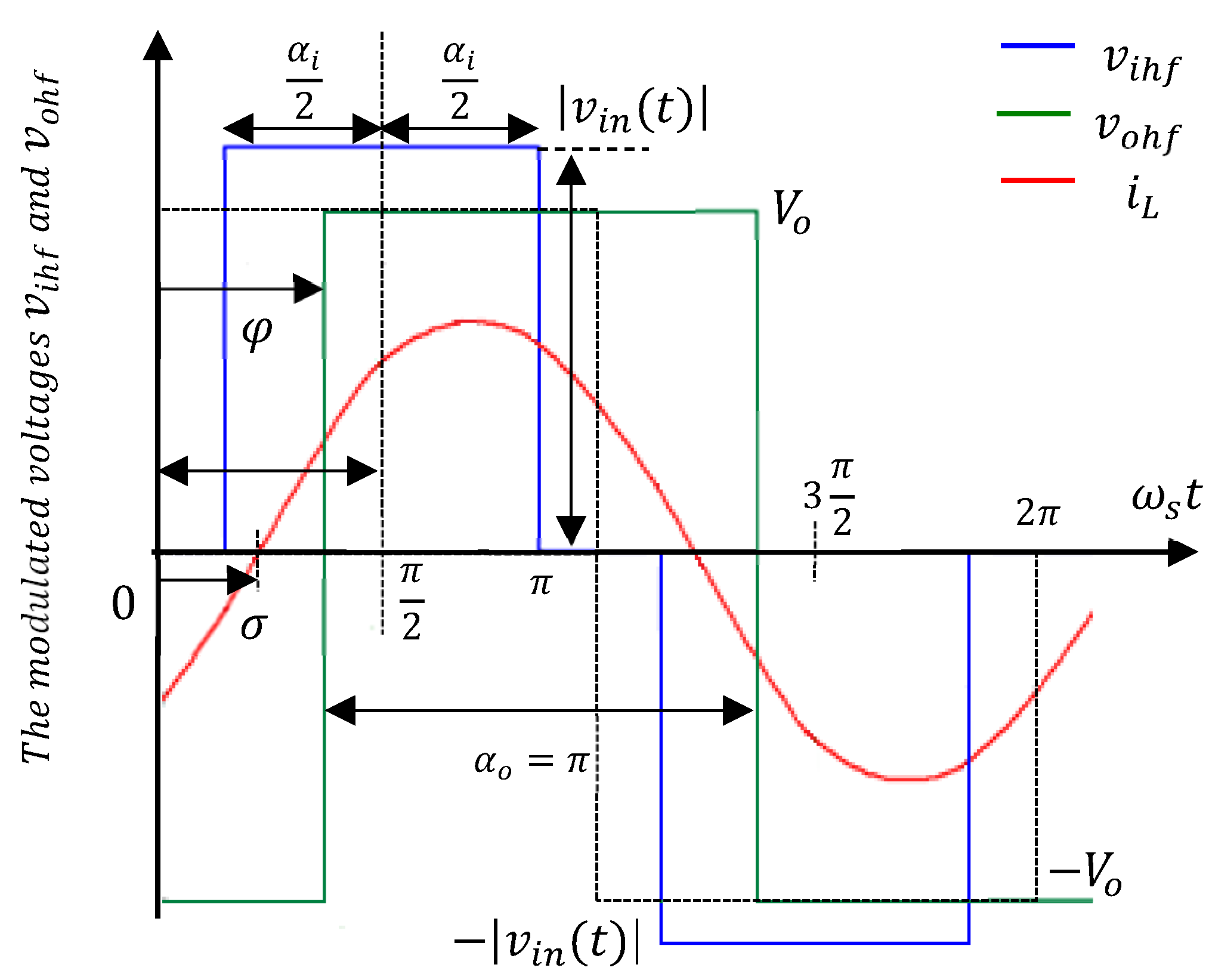
The modulated voltages and the SRC current are shown in Figure 8 for one switching period, considering DR α o 2 = π 2 (maximum value). Therefore, for grid-to-vehicle (G2V) power flow, the ZVS conditions for the QABSR DC–DC converter are:
{ i L < 0 ,   i n   ω s t = π 2 α i 2   ;   A C   s i d e   A B i L 0 ,   i n   ω s t = φ   ;   D C   s i d e   A B
Replacing (38) in (26), the ZVS conditions are provided by:
{ sin ( α i 2 ) > sin ( α i 2 + φ )   ;   A C   s i d e   A B 1 c o s ( φ )   ;   D C   s i d e   A B
where α i 2 (For i = a ,   b ,   c ) are the DR angles α a 2 , α b 2 or α c 2 . Evaluating (39), the AB on the DC side is always in ZVS mode. However, the ABs on the AC side lose the ZVS mode when the DR α i 2 takes small angle values. In fact, according to Figure 8, the ZVS is lost when ( π 2 α i 2 ) > σ .
A similar analysis can be performed for vehicle-to-grid (V2G) power flow. For this case, the four ABs are in ZVS mode even when the DR α a 2 , α b 2 , or α c 2 take small-angle values. Hence, this converter has lower switching losses in V2G mode than in G2V mode. However, for reactive power compensation α o 2 can take a small-angle value and the ZVS is affected on the DC-side AB. Hence, a compromise between obtaining a small HF current amplitude value and losing the ZVS mode must be taken.

3. Control Strategy

The average model for the controlled grid current i a considering the LF rectifier is shown in Figure 9a. An identical model can be used for the grid currents i b and i c . Note that the QABSR DC–DC converter is replaced by the average current source i a r provided by (30). This approximation is possible because the HF current dynamics of the QABSR DC–DC converter is faster than the grid current dynamics [51,52].
The average model for each rectified grid current is shown in Figure 9b where the LF rectifier and the grid voltage are replaced by the current source | i a | . Hence, the average model transfer function is provided by:
G i ( s ) = | i a | i a r = | i b | i b r = | i c | i c r = ω c 2   ( 1 + s r d C i ) s 2 + ( r d + R L L i ) s + ω c 2  
where ω c is the cutoff frequency of the L i C i filter provided by:
2 π f c = ω c = 1 L i C i
where r d and R L are the damping and the filter inductor resistances, respectively (see Figure 2), and i a r , i b r , and i c r are provided by (30). The closed-loop control strategy is shown in Figure 10 for the grid current i a r provided by (5). A similar control strategy is applied to i b and i c . Note that the rectified grid current i a r is controlled by the QABSR DC–DC converter whereas the LF rectifier unfolds the grid current i a (see Figure 2).
A PI controller cascaded with a first-order low-pass filter (LPF) with a cutoff frequency f L P F is used to obtain zero error at steady-state for | i a | . The frequency f L P F is chosen to attenuate 60 dB the harmonics at resonance frequency f c provided by (41), which means f L P F < f c 1000 . Whereas the PI is designed to compensate for the first harmonic of the rectified grid current at 2 ω g , where ω g is the grid frequency. Hence, the PI gains are chosen to have a closed-loop first-order system response with a bandwidth less than 2 ω g 10 .
The reference current generator block produces the time-variant reference currents | i a * | , i a r * using (2) and (5) and computes the DPFA θ . For these tasks, the voltage angle ω g t provided by the PLL, the active power P g * , and reactive power Q g * are required as inputs. Furthermore, using θ , the DR α o 2 is computed according to (36) or (37).
The rectified grid current i a r is controlled by the average current i a r provided by (30) where two command signals are used: the DR angle α a 2 and the PS angle φ . In ideal conditions (without losses in the converter and without the L i C i grid filter influence), α a 2 and φ are provided by (32) and (33), respectively. However, considering real conditions (losses and filter influence), a gain K c is added in the current control i a r amplitude as shown in (43). A similar control approach is applied to calculate α b 2 and α c 2 . Then, the DR angles α a 2 ,   α b 2 , and α c 2 , and the PSA φ are calculated with:
α a 2 = a s i n ( i a r K c I m ) ;   α b 2 = a s i n ( i b r K c I m ) ;   α c 2 = a s i n ( i c r K c I m ) ;  
φ = a sin ( K c I m K ) ;   Where   K c = 1.2
where I m and K are defined in (2) and (31), and the gain K c is chosen to have a real solution in (42), it means:
K c i a r I m ;   and   K c i b r I m ;   and   K c i c r I m ;  
Note that for light loads, the converter efficiency is decreased and the L i C i filter influence in the grid current is higher. Hence, K c can be increased by light loads. However, according to (43), high values of K c increases the angle φ , and by consequence, according to (28), increases the amplitude I L . Then, the gain K c must be chosen carefully with the aim of having minimum impact in the converter efficiency.

4. Converter Design

The proposed SSIB three-phase AC–DC converter was designed using the parameters in Table 1. First, the theoretical resonant inductance L r * and resonant capacitance C r * are calculated using (24) and (25), resulting L r * = 378.42 μH and C r * = 5.62 nF, respectively. Because the resonant capacitance is chosen for a commercial capacitance value, the capacitors 942C20S22K-F (22 nF) were selected whose series connection allows to obtain a capacitance value of C r = 5.5 nF. Therefore, the resonant inductor was recalculated to L r = 390 μH, which increases the quality factor to Q 4.1 .
Secondly, the turns ratio n is calculated using (23), which means n = V o 1 V e q 1 = V o 3 2 V m = 400 3 2 ( 220 2 ) 0.86 . Thirdly, for P o = 2 kW, the grid current amplitude is I m 4.29 A. The parameter K 5.27 is calculated with (31), and the phase-shift angle φ 54.4 ° using (32). The maximum HF current amplitude is calculated using (28) as I L 8.82 A.
The L i filter is designed to attenuate the switching frequency harmonics in the grid current. Note in Figure 9b that, L i and the DC-link capacitor C i behave as a second order LPF. Moreover, according to (40), the grid current dynamics depend on this filter. Since active bridge behaves as a rectifier for the HF current, the HF harmonics to be filtered in the grid current are provided by even harmonics 2 f s , 4 f s , etc. Hence, the cutoff frequency f c of the LPF shown in Figure 9b and provided by (41) is chosen to be f c < 2 f s 10 . Then C i = 1 μF and L i 200 μH are selected, with a cutoff frequency f c 11.25 kHz. Note that the DC link has a small capacitance value with the aim of having minimum impact on the reactive power injected into grid. Additionally, a damping resistor r d = 1.1 is used to decrease the L i C i resonance effect on the grid current [52,53]. The r d value was limited to generate losses of less than 1% of the nominal power.
Finally, the grid current controller is designed. The proposed control strategy is shown in Figure 10. The LPF cutoff frequency f L P F is chosen to attenuate 60 dB the harmonics at resonance frequency f c of the LPF provided by (41). Then f L P F < f c 1000 = 11.25 kHz 1000 11.25 Hz. Hence, the L i C i LPF was designed with a cutoff frequency f L P F = 10 Hz; whereas, the PI gains are chosen k p = 1 and k i 2 π f L P F k p with the aim of having a closed-loop first-order steady-state response at 10 Hz, to compensate for the first harmonic of the rectified grid current ( 2 ω g ). The bode plot for the average model transfer function G i ( s ) of the L i C i LPF provided by (40), the open-loop response P I ( s ) L P F ( s ) G i ( s ) , and the closed-loop response are shown in Figure 11a–c, respectively. Note in Figure 11b that the L i C i LPF resonance frequency peak is attenuated 60 dB, the phase margin (P.M.) is 90° and a bandwidth of 10 Hz is obtained according to the design. Finally, the closed-loop first-order response with a bandwidth of 10 Hz is depicted in Figure 11c.

5. Experimental Results

With the previous considerations, a three-phase AC–DC 2 kW prototype was built using the parameters in Table 2. Three HF transformers were built using ETD49 3C94 ferrite cores. The HF transformers series connection provides an equivalent total leakage inductance value of L 3 k 6 μH (each HF transformer has an equivalent leakage inductance of L 1 k 2 μH). The leakage inductance L 1 k 2 μH generates a small distortion in the HF current on the HF transformer primary side which does not affect the ZVS mode on the active bridge. The resonant inductor was implemented with an EE55 3C94 ferrite core for a L r * 384 μH. Note that L 3 k is much smaller than L r * . Hence, the leakage inductances of HF transformers have a minimal effect on the converter functionality [51]. Moreover, L r * + L 3 k = L r 390 μH which is indicated in Table 2.
The experimental setup is shown in Figure 12. To validate the bidirectional power flow in the grid, a 3Ø AC source and a 3Ø resistive load in parallel were used. Similarly, a bidirectional source was used on the DC side. Each grid voltage is connected to the converter at the zero-voltage crossing using bidirectional switches (see Figure 2) unlike typical VSI where a DC-link pre-charge is required [54].
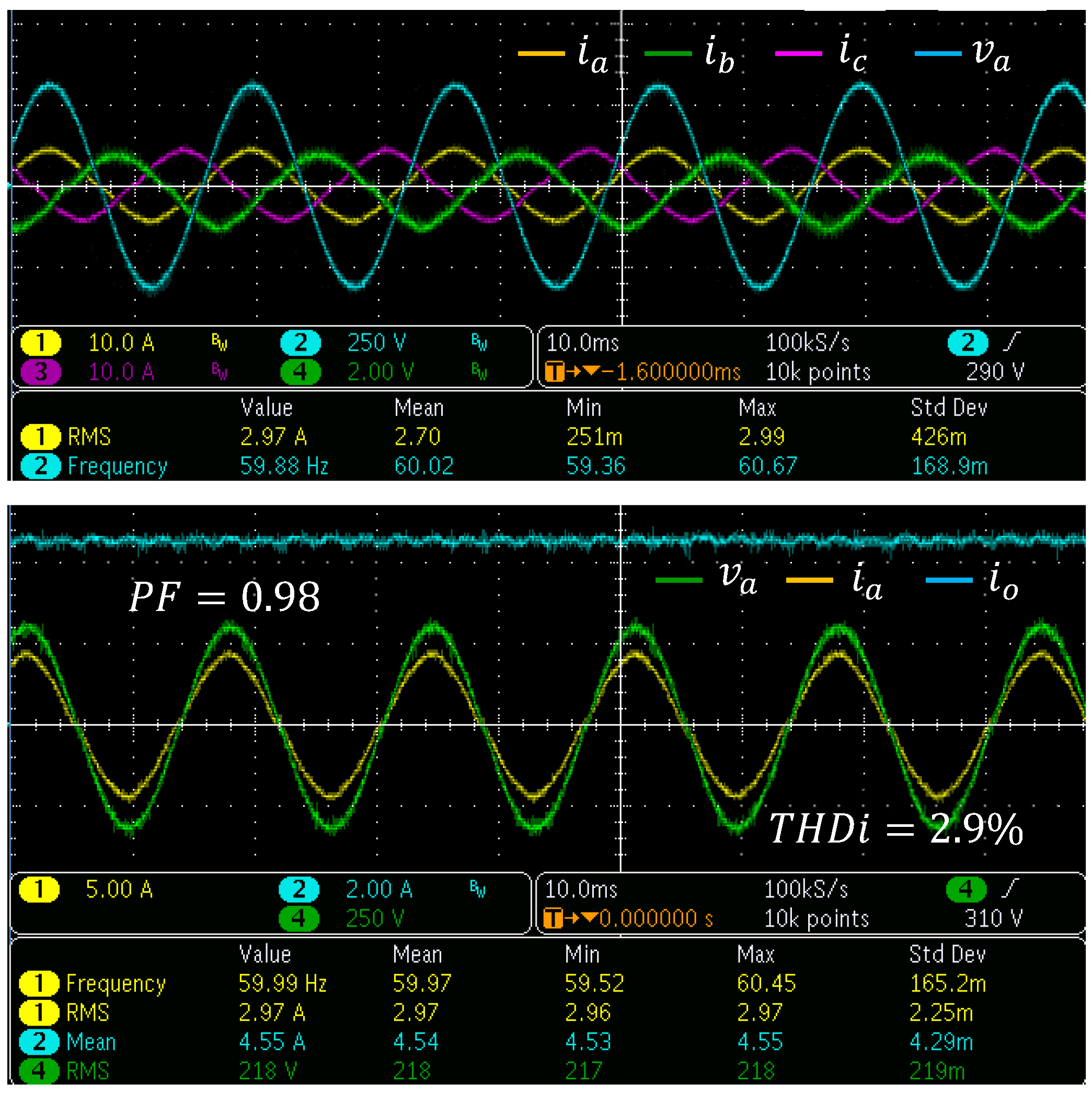
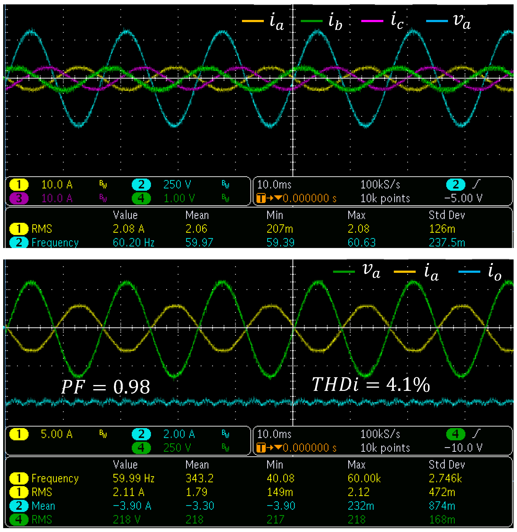
The results for the bidirectional power flow are shown in Figure 13 and Figure 14, respectively. The grid current parameters were measured using the single-phase power analyzer PA1000. In these two first analyzed cases, only bidirectional active power was tested.
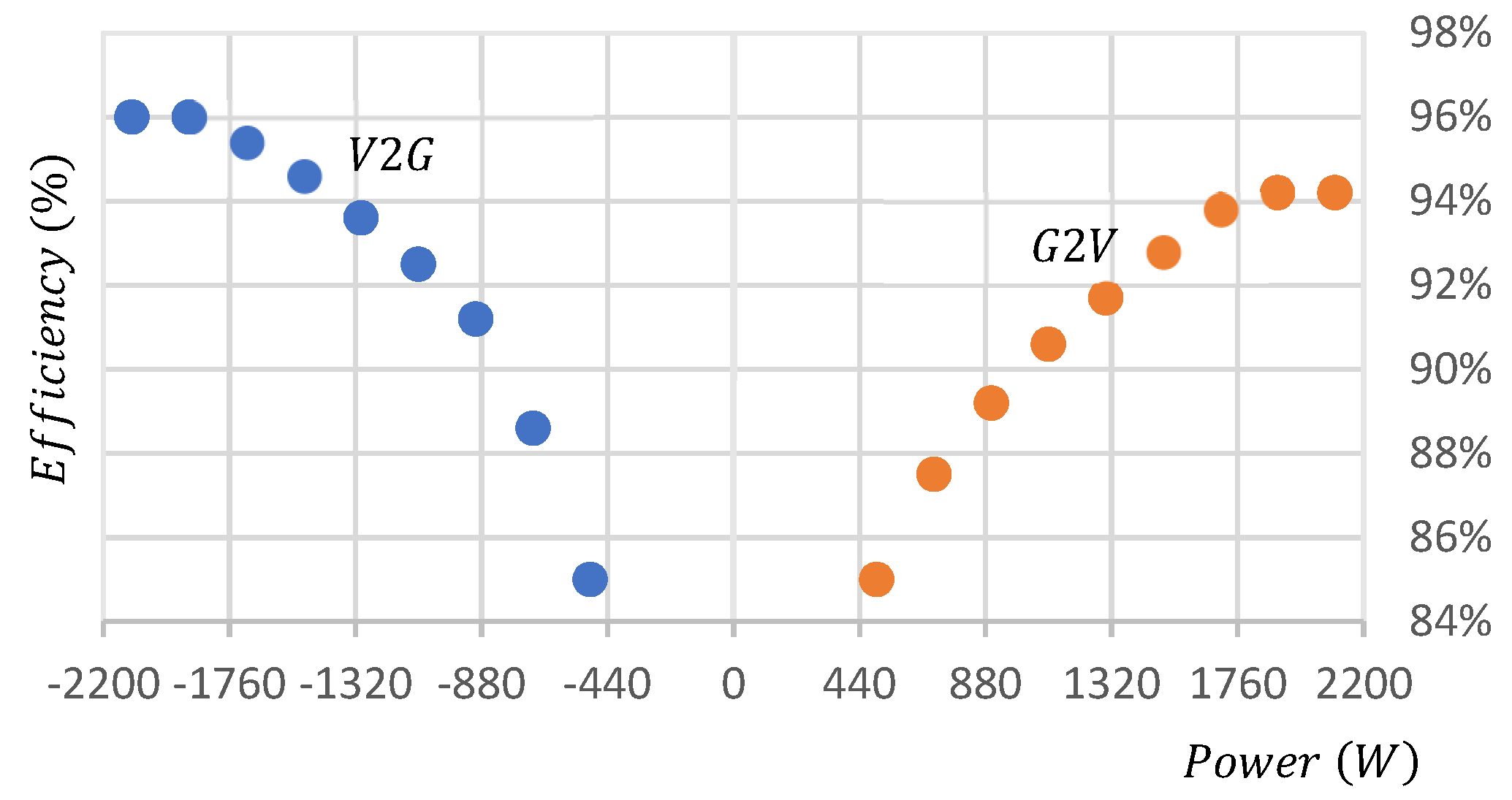
Note that three-phase balanced currents were obtained with the proposed modulation with a real power factor (PF) close to unity (PF = 0.98). Moreover, a very small total harmonic distortion in the grid current (THDi) was obtained for bidirectional power flow. Nonetheless, the THDi was slightly increased in V2G power flow, as shown in Figure 14. The DC source power was measured using a digital multimeter. The maximum measured efficiencies were 94.5% and 96%, respectively. The highest efficiency was obtained in V2G power flow because the four ABs were in ZVS mode. In contrast, in G2V power flow, ZVS mode is lost on the AC-side ABs when the DR α a 2 ,   α b 2 and α c 2 take small angle values.
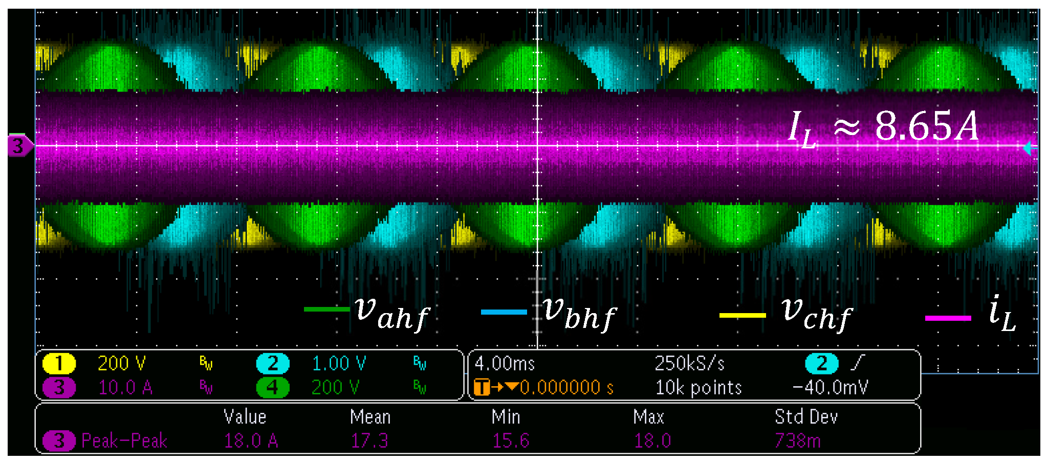
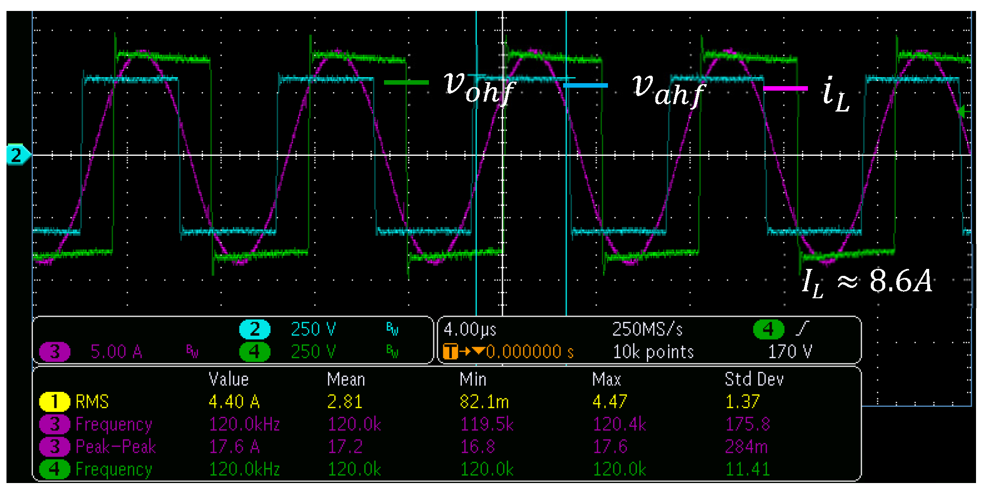
The HF three-phase power decoupling is validated in Figure 15. Note that the HF current has a constant amplitude for two grid periods. The calculated amplitude using (28) was I L 8.82 A whereas the oscilloscope measurement was 8.65 A approximately. This difference is due to the converter losses and the current probe accuracy.
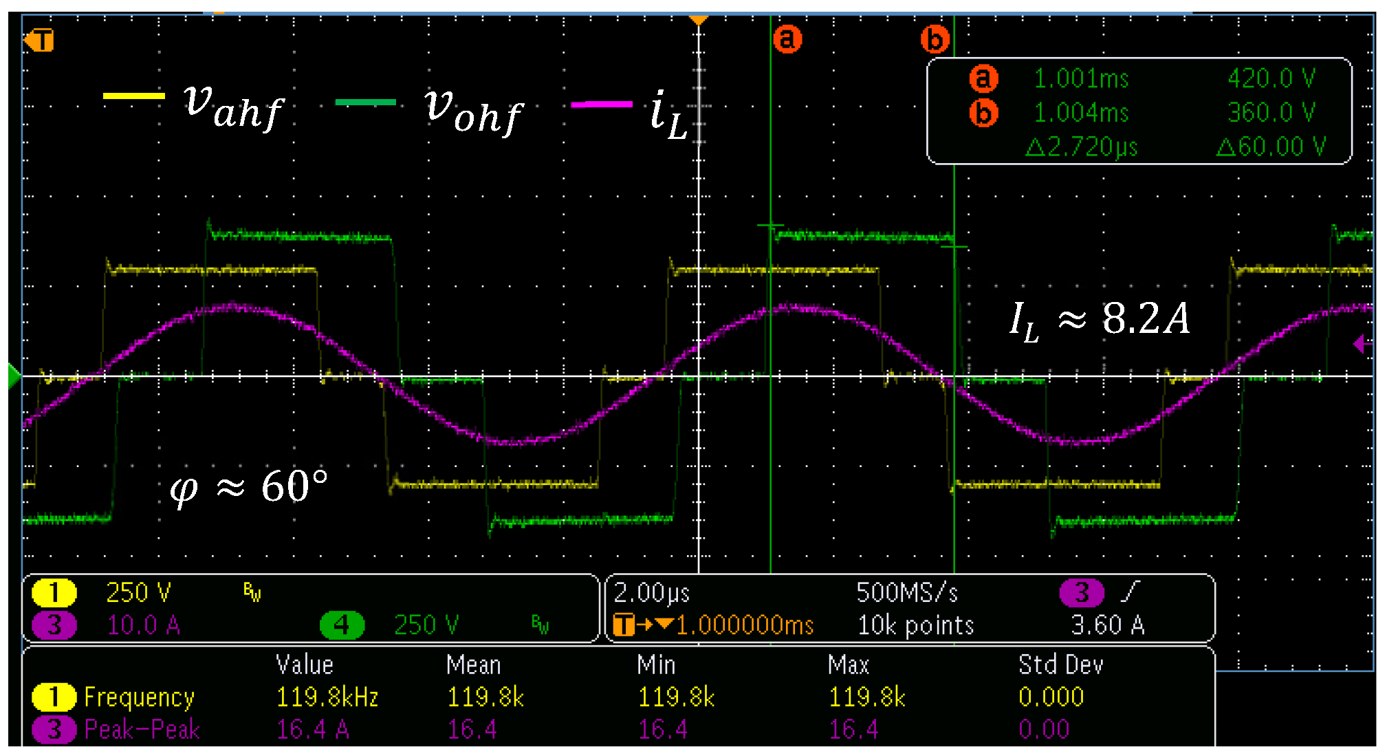
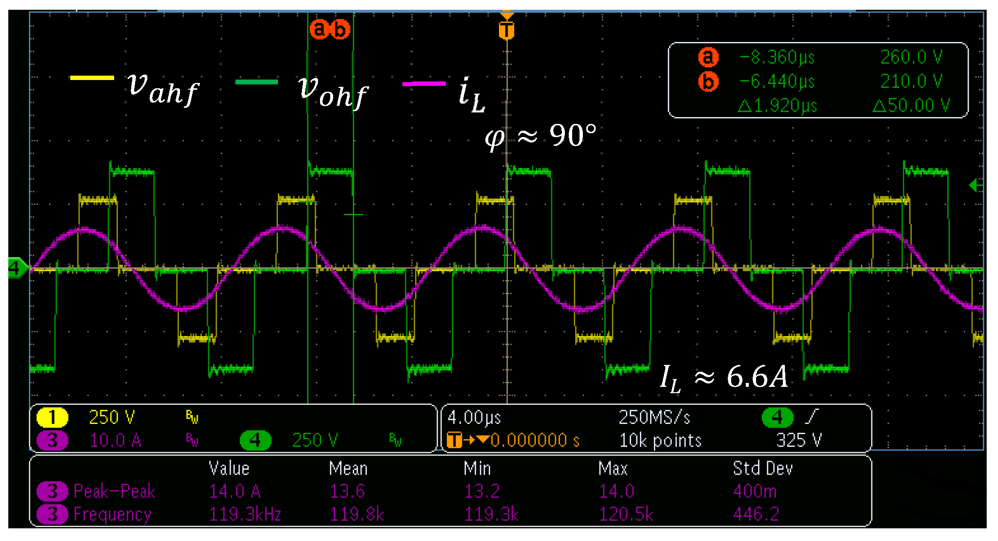
On the other hand, the modulated voltages v a h f and v o h f are shown for five switching periods considering ( α o 2 = π 2 ) . Note in Figure 16 that, for the G2V power flow case, both ABs switch in ZVS mode when the DR α a 2 takes angle values close to π 2 . However, ZVS is lost in one leg of the AC-side AB when the DR α a 2 takes small angle values, as shown in Figure 17.
Unlike G2V, for the V2G power flow case, ZVS mode is obtained for all angles of DR α a 2 as shown in Figure 18.
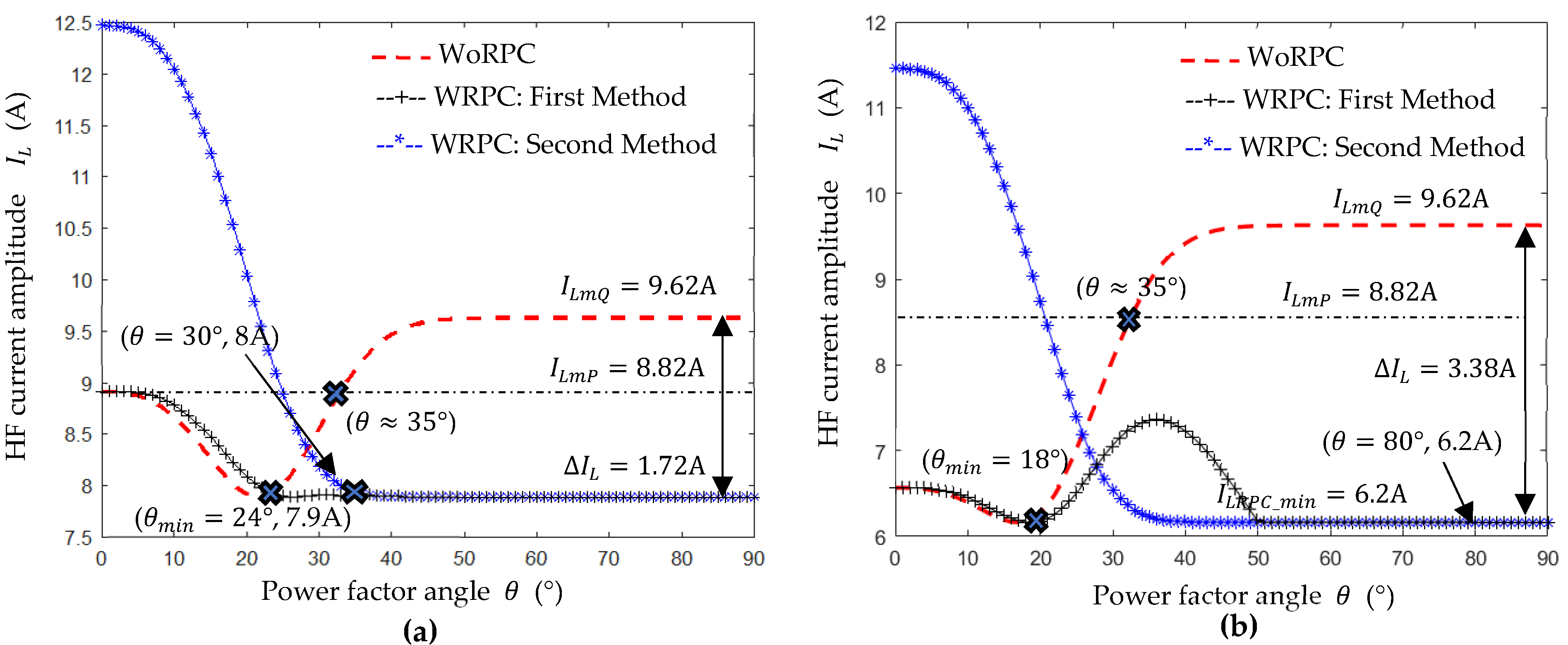
For reactive power injection capability analysis, the HF current I L was evaluated using (28), with and without reactive power compensation (WRPC and WoRPC, respectively). The results are shown in Figure 19 considering the apparent power S constant but shifting the displacement grid power factor angle (DPFA) θ from 0 ° to 90 ° . Two different cases were evaluated: S = 1.8 kVA and S = 1.5 kVA . Note that, for only active power injection, considering the nominal power P = 2 kW , the theoretically calculated HF current amplitude is I L m P = 8.82 A.
It can be noticed in Figure 19 that WoRPC ( α o 2 = π 2 ), the reactive power injection, can considerably increase the HF current amplitude I L . In fact, for both cases, if θ > 35 ° then, I L > I L m P = 8.82   A . Moreover, if θ > 50 ° then I L reaches its maximum value of I L m Q = 9.62   A . This means that, WoRPC, the HF transformers, must be oversized.
In change, I L decreases WRPC applying a DR α o 2 on the DC-side AB, according to (35). Indeed, in Figure 19a, if θ > 24 ° then I L _ W R P C < I L _ W o R P C while in Figure 19b, if θ > 18 ° then I L _ W R P C < I L _ W o R P C . Hence, a lookup table with the minimum values θ m i n can be used to implement the proposed RPC compensation. In a general case, the proposed reactive power compensation must be implemented if θ > 30 ° , which means the reactive power Q g is higher than the injected active power P . It should be noted that with the proposed reactive power compensation, for θ > 50°, the HF current I L can be decreased in approximately 18% for 1.8 kVA and 36% for 1.5 kVA, respectively. In none of these cases, the HF transformers need to be oversized because the reactive power injection impact is compensated. However, the efficiency is reduced due to the small DR applied which affects the ZVS mode.
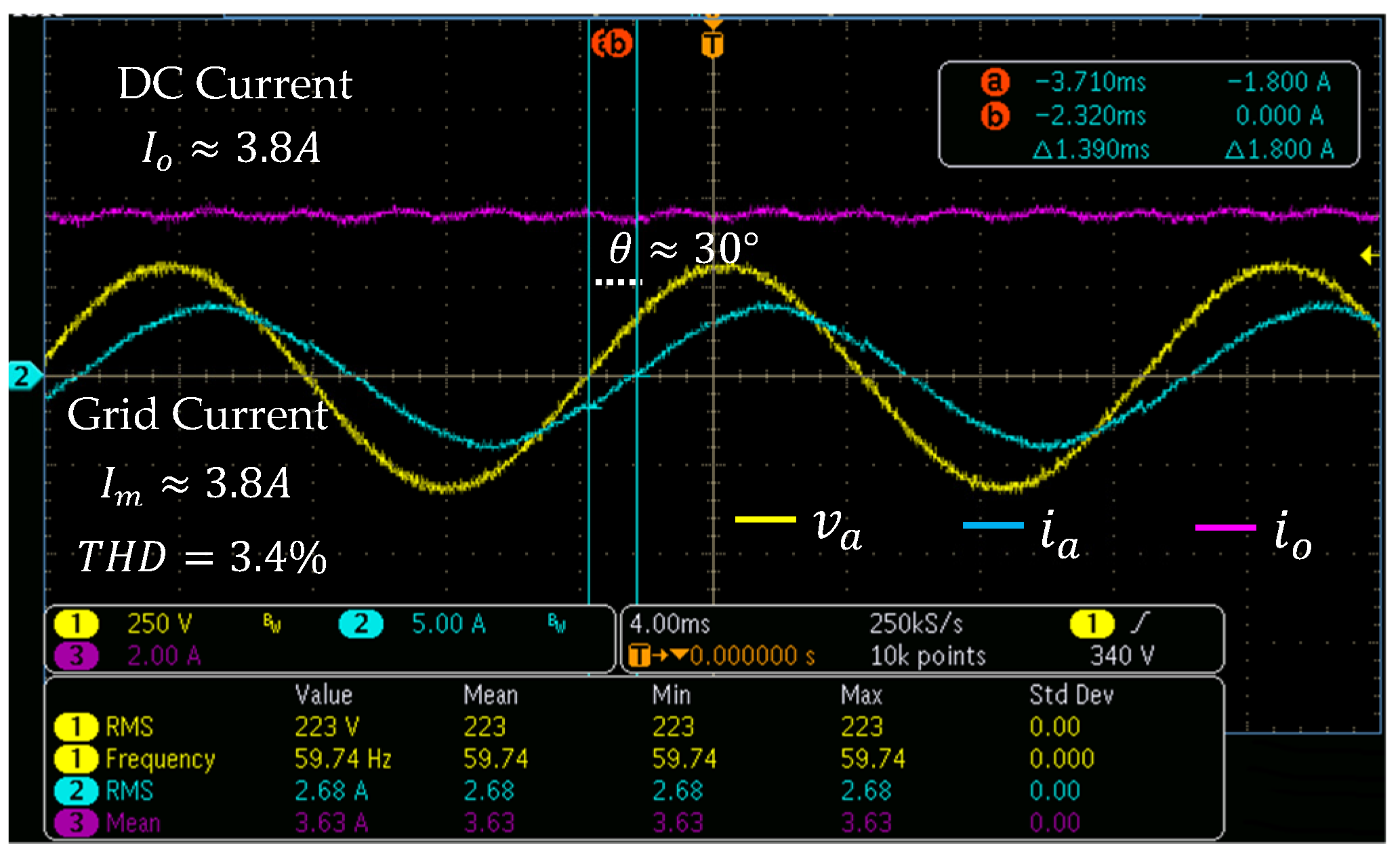
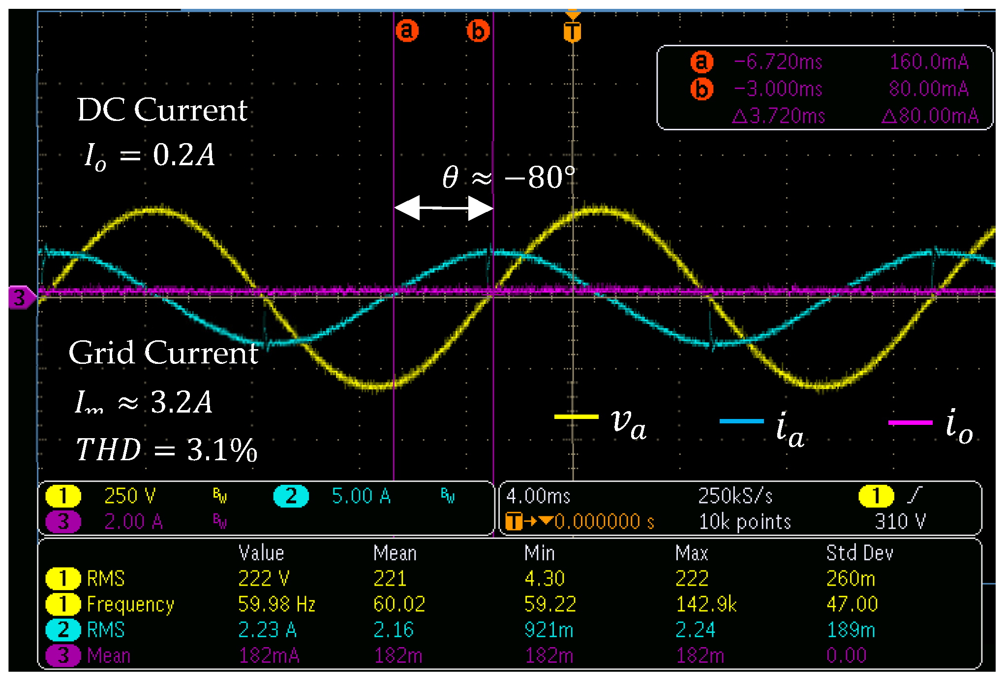
With the previous considerations, the grid reactive power compensation (RPC) results are shown in Figure 20 and Figure 21 for S = 1.8 kVA ( θ = 30°) and S = 1.5 kVA ( θ = 80°), in two grid periods, respectively.
Note in both cases that at each grid voltage zero-crossing, a slight distortion is generated in the grid current due to the current rectification by the LF rectifiers.
The modulated voltages and the HF current WRPC are shown in Figure 22 and Figure 23, applying a DR α o 2 = 60 ° and α o 2 = 42 ° , respectively. Note that the ZVS mode is obtained in both ABs and the HF current amplitude I L < I L m P = 8.82 A (current for the nominal active power P = 2 kW). The experimental results agree with analytical results shown in Figure 19.
On the other hand, the THDi values of grid currents were analyzed for different G2V power flow values, as shown in Figure 24.
In the case of light load, the THDi is increased. This drawback can be decreased if the gain of K c is increased (e.g., K c = 1.5 ) according to (43). However, this increase generates additional losses. Moreover, the THDi depends on the damping resistor r d value (see Figure 2). In the performed tests, the r d value was limited to generate losses of less than 1% of the nominal power. An alternative solution is to use an active damping current control to avoid the damping resistor [52,53]. Nonetheless, the current sensor connection for active damping is challenging in this structure.
The efficiency analysis for V2G and G2V is shown in Figure 25.
The converter achieves a high efficiency for the nominal power. However, the efficiency is lower for lighter loads. Furthermore, the highest efficiency is obtained in V2G power flow because ZVS mode is obtained in all ABs, unlike G2V power flow, where ZVS mode is lost in the three ABs on the AC side when the DRs take small angle values.
The losses distribution for the prototype at 2000 W is presented in Figure 26. The converter losses were not optimized because the aim was to validate the converter functionality. The highest losses obtained are conduction losses because of the MOSFETs quantity. These losses can be reduced using switches with the lowest resistance. However, this implies increasing the converter price. The switching losses can also be reduced by decreasing the switching frequency. Nevertheless, the volume of the resonant inductor and HF transformers increase as the switching frequency decreases. The optimization techniques to minimize converter losses were not covered in this article. Future studies will be focused on this subject.

6. Discussion

With the aim of highlighting the advantages of the proposed converter and modulation, unbalanced grid voltage conditions, and comparison with other structures are discussed in this section.

6.1. Unbalanced Voltages Conditions

The proposed converter was analyzed following the standard EN50160 which states that the unbalanced voltage degree should be below 2% over 95% of the time [55,56,57,58]. The steady-state response for the unbalanced grid voltage conditions indicated in (45) was analyzed. Note that the amplitude of the voltage v c n is decreased using the parameter a [ 0 1 ] , being the parameters V m and ω g = 2 π f g indicated in Table 2.
{ v a n = V m sin ( ω g t ) v b n = V m sin ( ω g t 2 π 3 ) v c n = ( 1 a ) V m sin ( ω g t + 2 π 3 )
Three balanced grid currents are controlled considering an amplitude I m 4.3 A and a voltage drop of a = 0.7 in (45). Unbalanced grid currents are not covered in this article. Simulation results are shown in Figure 27. Note in Figure 27a that, a LF ripple is present on the DC output current because of the unbalanced conditions. However, the grid currents are not affected, as shown in Figure 27b, because it depends on SCR parameters, the DC output voltage, (which are constants in a grid period), and the closed-loop control in the natural frame [59] implemented using the DR α a 2 , α b 2 and α c 2 as command signals.
To analyze the impact of the unbalanced grid voltages, provided in (45), on the HF current amplitude I L , the V e q 1 amplitude on the HF secondary side is recalculated using (16), then:
V e q 1 = ( 3 a ) 2 V m + a 2 V m cos ( 2 ω g t )
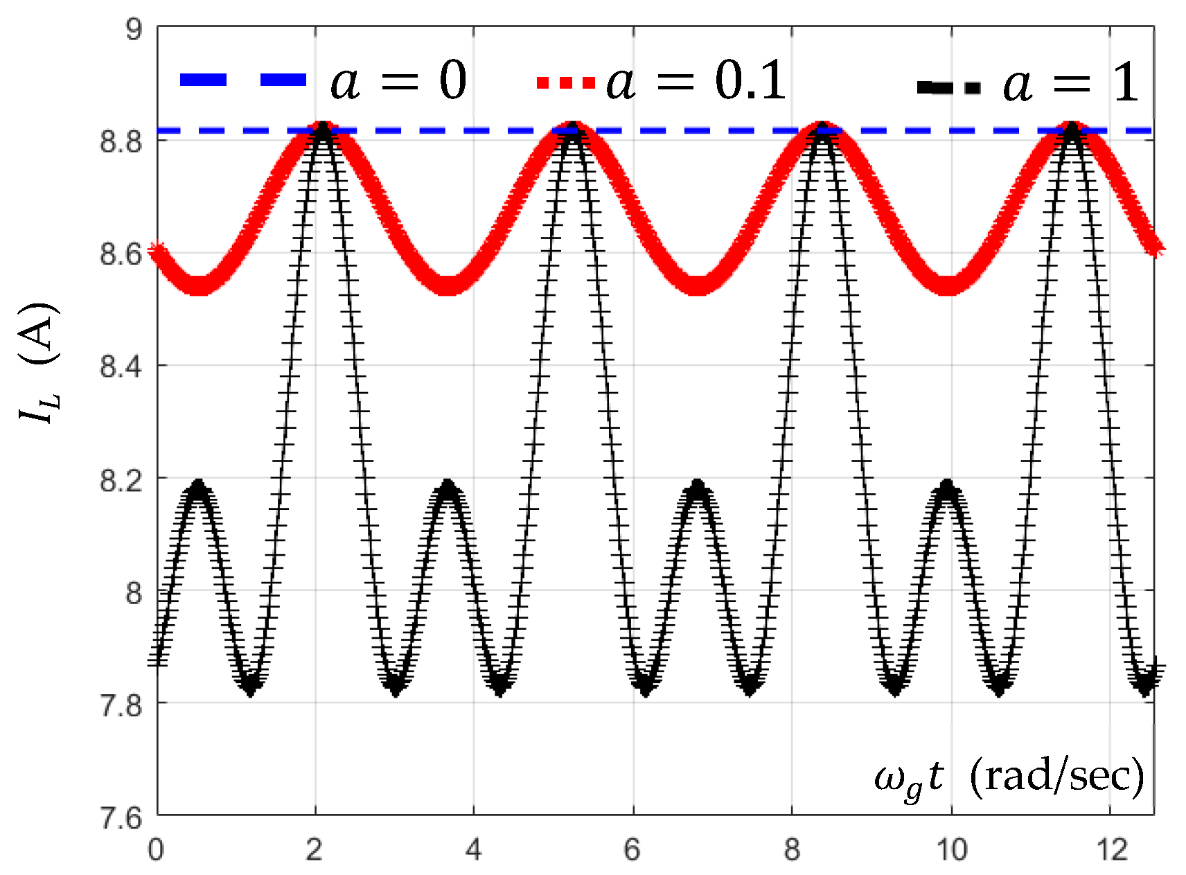
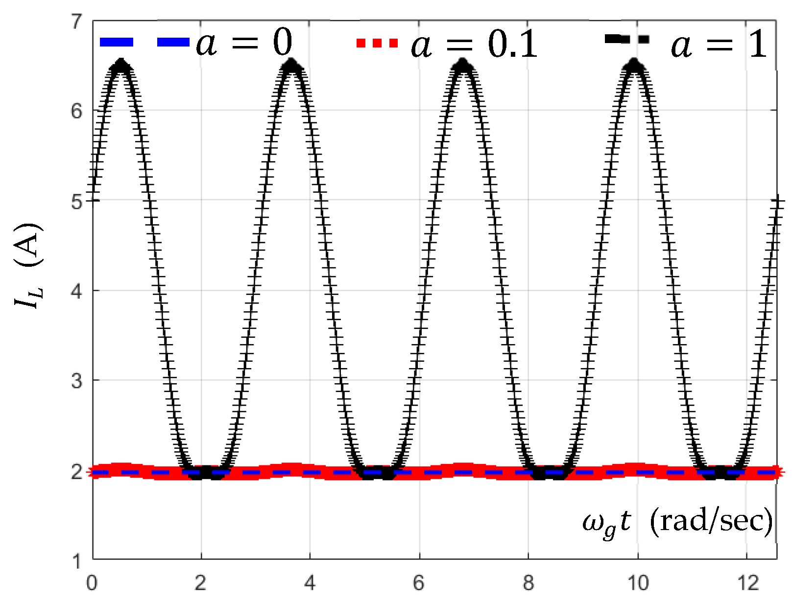
According to (46), a LF ripple variant at 2 ω g is present in V e q 1 . With this consideration, I L is calculated using (28). The results for three different voltage drops: a = 0 , a = 0.1 and a = 1 are shown in Figure 28 and Figure 29, respectively, considering the grid period scale and two different powers.
For a = 0 , HF three-phase power decoupling is obtained, which means the HF current has a constant amplitude. For a = 0.1 , a small LF ripple is obtained in the HF current amplitude. Hence, small unbalances according to the standard EN50160 have almost no effect on I L . In contrast, high unbalances ( a = 1 ) have a high impact on I L , particularly for small active power injection, as shown in Figure 29, where the HF amplitude is increased by 3.2 times compared with balanced voltages. However, in any case of grid voltages unbalance the HF current is lower than the nominal current I L ( m a x ) = 8.86 A. Thus, it the robustness of the proposed converter was proven since it can support voltage drops without overcurrent that can damage the converter.

6.2. Comparison with Single-Stage DC–AC Converters

A brief comparison with similar single-stage AC–DC structures [29,30] is shown in Table 3. In [29], three independent DABs were used (see Figure 1a). A similar approach can be implemented using three SSIB single-phase DABSR AC–DC converters [60]. However more SRC are required. Moreover, for that case, each SRC must be designed considering the single-phase time-variant power (whose maximum value is the double of the nominal power), and the converter size must be increased [50]. Hence, the use of three-series-connected HF transformers on the secondary side, one SRC, and the proposed modulation, allowing three-phase power decoupling and compensating for the high DC ripple, is a better option. In contrast, the three rectifiers were avoided in [30] because a DC offset was added in the neutral reference of the grid (see Figure 1b). However, HF transformers and the MOSFETs on the AC side must be sized for double the voltage compared with the proposed converter. Although the QAB structures are quite similar, according to (12) and (14), the HF three-phase power decoupling was not obtained using only time-variant PS modulation as proposed in [30]. Besides that, the proposed modulation and the control strategy have less complexity. Similarly, in the proposed converter, a smaller grid current THDi is obtained (2.9%) and, the modulation and control are easier to implement.
On the other hand, regarding the power density of the proposed structure, this is limited because the resonant capacitor volume increases with the power, unlike [29], where only one HF inductor was used. Hence, future works will focus on replacing the SCR with one HF inductor to increase the power density. Finally, the proposed converter analyzes the reactive power injection and unbalanced grid conditions, unlike [29,30].

6.3. Comparison with Two-Stage AC–DC Converters

A brief comparison with the two-stage AC–DC converters proposed for SST [39] and for SBC [8] is shown in Table 4. In [39] a QAB DC–DC converter DC-linked to three Multilevel DC–AC converters was analyzed. This structure is similar to the converter proposed in this work. To make a direct comparison, only a two-level (2L) DC–AC converter was used. In contrast, in [8] a DAB DC-linked to 2L DC–AC was proposed. For comparison, a grid voltage of 220 V rms and 60 Hz was considered. The advantages of the proposed converter are detailed below.
First, the DC-link capacitors were compared. In the proposed converter three tiny film capacitors were used whose voltages are the rectified grid voltages (the average voltage is v d c 198 V). In contrast, in a two-stage DC–AC converter as [8,39], bulky electrolytic capacitors in the DC link were used, handled 400 V and 800 V DC (with very small ripple), respectively. This means, the average DC voltage was half compared with [39] and a quarter compared with [8]. Moreover, in the proposed converter, the capacitance value is considerably smaller (only 1 μF) compared with two-stage DC–AC converter. Additionally, it is well-known that film capacitors present high durability and smaller volume and weight, unlike DC-link electrolytic capacitors [61,62]. Hence, the proposed converter presents better durability performances and smallest DC-link capacitors with reduced volume and weight.
Second, the required L filter to grid interface is smaller. In the proposed converter, because the HF switching and small DC-link voltage, the L filter is smaller (200 µH) compared with [8,39]. The L filter in [8,39] can be reduced using an LCL filter, but the volume and the inductance value is even bigger compared with the L filter in the proposed converter. Hence, the proposed converter has the smallest L Filter, reducing the volume and weight of the converter.
Finally, the MOSFET quantity and the switching mode were compared. In the proposed converter each grid voltage is independently modulated. For this purpose, three LF single-phase (3-1 ϕ ) rectifiers linked with a QABSR DC–DC converter was used. Hence 28 MOSFETs were used. A similar structure was used in [39]. However, the functionality of the proposed converter is quite different because the rectifiers switch at LF and ZVS mode unlike [39] where the 3-1 ϕ VSIs switch at HF and hard-switching (HS) mode. Hence, the proposed converter presents higher efficiency. Instead, only 14 MOSFET were used in [8]. However, the VSI switches at HF and HS mode which affects the converter efficiency. This problem is increased by the bulky L filter, unlike the proposed converter where all the ABs switch at ZVS mode and uses smaller L filters. Hence, even if in the proposed converter the MOSFET quantity is greater, higher efficiency is obtained because the LF switching in rectifiers and the smaller L filters.
With all the comparisons and results, the proposed converter is a good candidate for SST and SBC applications because the high efficiency and durability, and the reduced volumes of DC-link capacitors and L filters. However, the proposed QAB power density can be improved even more using only inductive elements. Hence, future works will be focused on implementing the proposed modulation in a QAB DC–DC converter with only inductive elements.

7. Conclusions

A novel SSIB three-phase AC–DC converter composed of three LF rectifiers linked by tiny film capacitors with a QABSR DC–DC converter was presented. Because the LF rectifiers and the linking capacitances, the QABSR must manage: three DC inputs with high ripple (the rectified grid voltages), the active and reactive grid power injection, and assure minimum HF current. Because of that, a novel QABSR modulation, using fixed switching frequency, was introduced. The rectified grid voltages are modulated by time-variant duty ratio modulation whose angles change according to the grid current angles; whereas, the DC source is modulated by phase shift whose angle is calculated according to the grid current amplitude. The modulation and the HF transformers series-connected on the secondary side allow to compensate for the three DC inputs with high ripple. Thus, for a balanced three-phase system, the proposed modulation allows to obtain a HF current with a constant amplitude and minimum value, called in this article “HF three-phase power decoupling”. Therefore, the QABSR has a steady-state response as an equivalent DABSR DC–DC converter. Moreover, it is shown that high reactive power injection can considerably increase the HF current. Hence, a duty ratio angle on DC-side active bridge modulation is introduced to compensate for this increase. The results show that the HF current can be decreased by up to 35%. The proposed modulation allows to implement a decoupled grid current controller in the natural frame. Measurements demonstrate the converter functionality. Very low THD is obtained in the grid current, unlike similar structures. High efficiency is obtained due to the ZVS mode. The reactive power compensation performances were validated and the steady-state response for unbalanced grid conditions is discussed. A brief comparison with two-stage AC–DC converters shows that the proposed converter has smaller volume and greater durability as it uses tiny DC-link film capacitors and smaller L filters. Besides that, the proposed modulation can be implemented in similar QAB AC–DC structures with only inductive elements which will be validated in future projects. Hence, the proposed converter and modulation are a good alternative for solid-state transformers and EV Smart Battery Charger applications.

Author Contributions

D.S.y.R., D.C, D.F., and J.-P.F. contributed to the research, investigation, results analysis, resources, and writing—review and editing. All authors have read and agreed to the published version of the manuscript.

Funding

This research was supported by Concytec-Prociencia by the project “Manufactura Avanzada de Estaciones de recarga rápida de vehículos eléctricos basada en Sistemas Fotovoltaicos Inteligentes” [Contract N° 007-2021] and the UNI Project “FIEE-PFE-01-2022”.

Data Availability Statement

All the reported data are included in the manuscript.

Conflicts of Interest

The authors declare no conflict of interest.

References

  1. Hu, Q.; Bu, S.; Terzija, V. A Distributed P and Q Provision-Based Voltage Regulation Scheme by Incentivized EV Fleet Charging for Resistive Distribution Networks. IEEE Trans. Transp. Electrif. 2021, 7, 2376–2389. [Google Scholar] [CrossRef]
  2. Restrepo, M.; Morris, J.; Kazerani, M.; Cañizares, C.A. Modeling and Testing of a Bidirectional Smart Charger for Distribution System EV Integration. IEEE Trans. Smart Grid 2018, 9, 152–162. [Google Scholar] [CrossRef]
  3. Zheng, L.; Marellapudi, A.; Chowdhury, V.R.; Bilakanti, N.; Kandula, R.P.; Saeedifard, M.; Grijalva, S.; Divan, D. Solid-State Transformer and Hybrid Transformer with Integrated Energy Storage in Active Distribution Grids: Technical and Economic Comparison, Dispatch, and Control. IEEE J. Emerg. Sel. Top. Power Electron. 2022, 10, 3771–3787. [Google Scholar] [CrossRef]
  4. Mahammad, A.H.; Ker, P.J.; Lipu, M.S.H.; Choi, Z.H.; Rahman, M.S.A.; Muttaqi, K.M.; Blaabjerg, F. State of the Art of Solid-State Transformers: Advanced Topologies, Implementation Issues, Recent Progress and Improvements. J. IEEE Access 2020, 8, 19113–19132. [Google Scholar]
  5. Da Silva, R.L.; Borges, V.L.F.; Possamai, C.E.; Barbi, A.I. Solid-State Transformer for Power Distribution Grid Based on a Hybrid Switched-Capacitor LLC-SRC Converter: Analysis, Design, and Experimentation. J. IEEE Access 2020, 8, 141182–141207. [Google Scholar] [CrossRef]
  6. Rasool, H.; Verbrugge, B.; Zhaksylyk, A.; Tran, T.M.; el Baghdadi, M.; Hegazy, T.G.A.O. Design Optimization and Electro-Thermal Modeling of an Off-Board Charging System for Electric Bus Applications. J. IEEE Access 2021, 9, 84501–84519. [Google Scholar] [CrossRef]
  7. Khan, S.; Islam, M.; Guo, Y.; Zhu, J. A New Isolated Multi-Port Converter with Multi-Directional Power Flow Capabilities for Smart Electric Vehicle Charging Stations IEEE Trans. Appl. Supercond. 2019, 29, 1–4. [Google Scholar]
  8. Mejía-Ruiz, G.; Paternina, M.R.A.; Rodriguez, J.R.; Zamora, A.; Bolivar-Ortiz, G.; Toledo-Santos, C. A bidirectional isolated charger for electric vehicles in V2G systems with the capacity to provide ancillary services. In Proceedings of the 2020 52nd North American Power Symposium (NAPS), Tempe, AS, USA, 11–14 April 2021. [Google Scholar] [CrossRef]
  9. Fang, J.; Li, H.; Tang, Y. A Magnetic Integrated LLCL Filter for Grid-Connected Voltage-Source Converters. IEEE Trans. Power Electron. 2017, 32, 1725–1730. [Google Scholar] [CrossRef]
  10. Peña, J.; Espinoza, R.; Rosas, D.S.Y. Single stage AC-DC bidirectional converter with high frequency galvanic isolation suitable for V2G applications. In Proceedings of the Energy Conversion Congress and Exposition—Asia, Virtual Conference, 24–27 May 2021. [Google Scholar] [CrossRef]
  11. Sayed, M.; Suzuki, K.; Takeshita, T.; Kitagawa, W. PWM Switching Technique for Three-Phase Bidirectional Grid-Tie DC–AC–AC Converter with High-Frequency Isolation. IEEE Trans. Power Electron. 2018, 33, 845–858. [Google Scholar] [CrossRef]
  12. Das, D.; Weise, N.; Basu, K.; Baranwal, R.; Mohan, N. A Bidirectional Soft-Switched DAB-Based Single-Stage Three-Phase AC–DC Converter for V2G Application. IEEE Trans. Transp. Electrif. 2019, 5, 186–199. [Google Scholar] [CrossRef]
  13. Amirabadi, M.; Baek, J.; Toliyat, H. Bidirectional Soft-Switching Series AC-Link Inverter. IEEE Trans. Ind. Appl. 2015, 51, 2312–2320. [Google Scholar] [CrossRef]
  14. Wu, F.; Li, X.; Yang, G.; Liu, H.; Meng, T. Variable Switching Periods Based Space Vector Phase-Shifted Modulation for DAB Based Three-Phase Single-Stage Isolated AC–DC Converter. IEEE Trans. Power Electron. 2020, 35, 13725–13734. [Google Scholar] [CrossRef]
  15. Li, X.; Wu, F.; Yang, G.; Liu, H.; Meng, T. Dual-Period-Decoupled Space Vector Phase-Shifted Modulation for DAB-Based Three-Phase Single-Stage AC–DC Converter. IEEE Trans. Power Electron. 2020, 35, 6447–6457. [Google Scholar] [CrossRef]
  16. Liu, Y.; He, J.; Ge, B.; Li, X.; Xue, Y.; Blaabjerg, F. A Simple Space Vector Modulation of High-Frequency AC Linked Three-Phase-to-Single-Phase/DC Converter. IEEE Access J. 2020, 8, 59278–59289. [Google Scholar] [CrossRef]
  17. Sal y Rosas, D.; Andrade, J.; Frey, D.; Ferrieux, J.-P. Single stage isolated bidirectional DC/AC Three-phase converter with a series-resonant Circuit for V2G. In Proceedings of the Vehicle Power and Propulsion Conference (VPPC), Belfort, France, 27–30 August 2017. [Google Scholar]
  18. Andrade, J.; Rosas, D.S.Y.; Frey, D.; Ferrieux, J.-P. Modified triple active bridge DC/AC three-phase converter with a series-resonant LC circuit on the AC-side. In Proceedings of the SPEC, L’Aquila, Italy, 22–26 April 2017. [Google Scholar]
  19. Gu, L.; Jin, K. A Three-Phase Isolated Bidirectional AC/DC Converter and its Modified SVPWM Algorithm. IEEE Trans. Power Electron. 2015, 30, 6447–6457. [Google Scholar] [CrossRef]
  20. Saha, J.; Singh, R.K.; Panda, S.K. Three-phase matrix-based isolated AC-DC converter for battery energy storage system. In Proceedings of the PEDG, Virtual Conference, 28 June–1 July 2021. [Google Scholar] [CrossRef]
  21. Varajao, D.; Aráujo, R.E.; Miranda, L.M.; Lopes, J. Modulation Strategy for a Single-Stage Bidirectional and Isolated AC–DC Matrix Converter for Energy Storage Systems. IEEE Trans. Ind. Appl. 2018, 65, 3458–3468. [Google Scholar] [CrossRef]
  22. Prabu, A.; Sridhar, A.; Weise, N. Bidirectional SiC three-phase AC-DC Converter with DQ current control. In Proceedings of the ECCE, Montreal, QC, Canada, 20–24 September 2015. [Google Scholar] [CrossRef]
  23. Shigeuchi, K.; Xu, J.; Shimosato, N.; Sato, Y. A Modulation Method to Realize Sinusoidal Line Current for Bidirectional Isolated Three-Phase AC/DC Dual-Active-Bridge Converter Based on Matrix Converter. IEEE Trans. Power Electron. 2021, 36, 6015–6029. [Google Scholar] [CrossRef]
  24. Malekjamshidi, Z.; Jafari, M.; Zhang, J.; Zhu, J. Design and analysis of protection circuits for safe operation of direct matrix converters. In Proceedings of the The 3rd International Conference on Education in Muslim Society (ICEMS 2017), Banten, Indonesia, 25–26 October 2017. [Google Scholar] [CrossRef]
  25. Chen, W.W.; Zane, R.; Corradini, L. Isolated Bidirectional Grid-Tied Three-Phase AC–DC Power Conversion Using Series-Resonant Converter Modules and a Three-Phase Unfolder. IEEE Trans. Power Electron. 2017, 32, 9001–9012. [Google Scholar] [CrossRef]
  26. Das, D.; Basu, K. A Soft-switched isolated single stage bidirectional three phase AC-DC converter. In Proceedings of the ECCE, Baltimore, MD, USA, 29 September—3 October 2019. [Google Scholar] [CrossRef]
  27. Yelaverthi, D.B.; Mansour, M.; Wang, H.; Zane, R. Triple Active Bridge Series Resonant converter for three phase unfolding based isolated converters. In Proceedings of the IECON, Lisbon, Portugal, 14–17 October 2019. [Google Scholar] [CrossRef]
  28. Gu, L.; Peng, K. A single-stage isolated three-phase bidirectional AC/DC converter for high power applications. In Proceedings of the ECCE, Baltimore, MD, USA, 29 September—3 October 2019. [Google Scholar] [CrossRef]
  29. Waltrich, G.; Duarte, J.L.; Hendrix, M.A.M. Three-phase bidirectional dc/ac converter using a six-leg inverter connected to a direct ac/ac converter. IET Power Electron. J. 2015, 8, 2214–2222. [Google Scholar] [CrossRef]
  30. Chan, Y.P.; Loo, K.H.; Lai, Y.M. Single-stage immittance-based three-phase AC-DC bidirectional converter and PWM strategy for realizing zero circulating power. In Proceedings of the EPE’2017, Warsaw, Poland, 11–14 September 2017. [Google Scholar] [CrossRef]
  31. Lu, J.; Bai, K.; Taylor, A.R.; Liu, G.; Brown, A.; Johnson, P.; McAmmond, M. A Modular-Designed Three-Phase High-Efficiency High-Power-Density EV Battery Charger Using Dual/Triple-Phase-Shift Control. IEEE Trans. Power Electron. 2018, 33, 8091–8100. [Google Scholar] [CrossRef]
  32. Vermulst, B.; Duarte, J.L.; Wijnands, C.G.E.; Lomonova, E. Quad-Active-Bridge Single-Stage Bidirectional Three-Phase AC–DC Converter with Isolation: Introduction and Optimized Modulation. IEEE Trans. Power Electron. 2017, 32, 2546–2557. [Google Scholar] [CrossRef] [Green Version]
  33. Haider, M.; Anderson, J.A.; Miric, S.; Nain, N.; Zulauf, G.; Kolar, J.W.; Xu, D.; Deboy, G. Novel ZVS S-TCM Modulation of Three-Phase AC/DC Converters. IEEE Open J. Power Electron. 2020, 1, 529–543. [Google Scholar] [CrossRef]
  34. Sal y Rosas, D. Isolated and bidirectional three-phase AC-DC converter composed of three unfolding bridges cascaded with a quad-active-bridge series-resonant DC-DC converter. In Proceedings of the EPE’2021, Virtual Conference, 6–10 September 2021. [Google Scholar]
  35. Costa, L.F.; Buticchi, G.; Liserre, M. Quad-Active-Bridge DC–DC Converter as Cross-Link for Medium-Voltage Modular Inverters. IEEE Trans. Ind. Appl. 2017, 53, 1243–1253. [Google Scholar] [CrossRef]
  36. Li, X.; Cheng, L.; He, L.; Wang, C.; Zhu, Z. Decoupling Control of an LLC-Quad-active bridge Cascaded Power Electronic Transformer based on Accurate Small-signal Modeling. IEEE J. Emerg. Sel. Top. Power Electron. 2021, 10, 4115–4127. [Google Scholar] [CrossRef]
  37. Nair, A.C.; Fernandes, B.G. Solid-State Transformer Based Fast Charging Station for Various Categories of Electric Vehicles with Batteries of Vastly Different Ratings. IEEE Trans. Ind. Electron. 2021, 68, 10400–10411. [Google Scholar] [CrossRef]
  38. Achanta, P.; Maksimovic, D.; Johnson, B. Cascaded quadruple active bridge structures for multilevel DC to three-phase AC conversion. In Proceedings of the APEC, San Antonio, TX, USA, 4–8 March 2018. [Google Scholar] [CrossRef]
  39. Achanta, P.K.; Johnson, B.B.; Seo, G.-S.; Maksimovic, D. A Multilevel DC to Three-Phase AC Architecture for Photovoltaic Power Plants. IEEE Trans. Energy Convers. 2019, 34, 181–190. [Google Scholar] [CrossRef]
  40. Gong, S.; Li, X.; Han, J.; Sun, Y.; Xu, G.; Jiang, Y.; Huang, S. Sliding Mode Control-Based Decoupling Scheme for Quad-Active Bridge DC–DC Converter. IEEE J. Emerg. Sel. Top. Power Electron. 2022, 10, 1153–1164. [Google Scholar] [CrossRef]
  41. Falcones, S.; Ayyanar, R.; Mao, X. A DC–DC Multiport-Converter-Based Solid-State Transformer Integrating Distributed Generation and Storage. IEEE Trans. Power Electron. 2013, 28, 2192–2203. [Google Scholar] [CrossRef]
  42. Naseem, N.; Cha, H. Quad-Active-Bridge Converter with Current Balancing Coupled Inductor for SST Application. IEEE Trans. Power Electron. 2021, 36, 12528–12539. [Google Scholar] [CrossRef]
  43. Hebala, O.M.; Aboushady, A.A.; Khaled, H. Ahmed and Ibrahim Abdelsalam, Generalized Active Power Flow Controller for Multiactive Bridge DC–DC Converters with Minimum-Current-Point-Tracking Algorithm. IEEE Trans. Ind. Electron. 2022, 69, 3764–3775. [Google Scholar] [CrossRef]
  44. Yang, J.; Buticchi, G.; Gu, C.; Günter, S.; Zhang, H.; Wheeler, P. A Generalized Input Impedance Model of Multiple Active Bridge Converter. IEEE Trans. Transp. Electrif. 2020, 6, 1695–1706. [Google Scholar] [CrossRef]
  45. Bandyopadhyay, S.; Qin, Z.; Bauer, P. Decoupling Control of Multiactive Bridge Converters Using Linear Active Disturbance Rejection. IEEE Trans. Ind. Electron. 2021, 68, 10688–10698. [Google Scholar] [CrossRef]
  46. Rahman, M.A.; Islam, M.R.; Muttaqi, K.M.; Sutanto, D. Modeling and Control of SiC-Based High-Frequency Magnetic Linked Converter for Next Generation Solid State Transformers. IEEE Trans. Energy Convers. 2020, 35, 549–559. [Google Scholar] [CrossRef]
  47. Gu, C.; Yan, H.; Yang, J.; Sala, G.; de Gaetano, D.; Wang, X.; Galassini, A.; Degano, M.; Zhang, X.; Buticchi, G. A Multiport Power Conversion System for the More Electric Aircraft. IEEE Trans. Transp. Electrif. 2020, 6, 1707–1720. [Google Scholar] [CrossRef]
  48. Dursun, M.; Döşoğlu, M.K. LCL Filter design for grid connected three-phase inverter. In Proceedings of the ISMSIT, Ankara, Turkey, 19–21 October 2018. [Google Scholar] [CrossRef]
  49. Hrectifierer, J.E.; Kolar, J.W. Applicability of Solid-State Transformers in Today’s and Future Distribution Grids. IEEE Trans. Smart Grid 2019, 10, 317–326. [Google Scholar]
  50. Sal y Rosas, D.; Frey, D.; Ferrieux, J.-P. Isolated single stage bidirectional AC-DC converter with power decoupling and reactive power control to interface battery with the single-phase grid. In Proceedings of the APEC, San Antonio, TX, USA, 4–8 March 2018. [Google Scholar]
  51. Krishnaswami, H.; Mohan, N. Three-Port Series-Resonant DC–DC Converter to Interface Renewable Energy Sources with Bidirectional Load and Energy Storage Ports. IEEE Trans. Power Electron. 2009, 24, 2289–2299. [Google Scholar] [CrossRef]
  52. He, Y.; Wang, X.; Ruan, X.; Pan, D.; Xu, X.; Liu, F. Capacitor-Current Proportional-Integral Positive Feedback Active Damping for LCL-Type Grid-Connected Inverter to Achieve High Robustness Against Grid Impedance Variation. IEEE Trans. Power Electron. 2019, 34, 12423–12436. [Google Scholar] [CrossRef]
  53. Pan, D.; Ruan, X.; Wang, X.; Yu, H.; Xing, Z. Analysis and Design of Current Control Schemes for LCL-Type Grid-Connected Inverter Based on a General Mathematical Model. IEEE Trans. Power Electron. 2017, 32, 4395–4410. [Google Scholar] [CrossRef]
  54. Langbauer, T.; Connaughton, A.; Vollmaier, F.; Krischan, K. Pre-charging of a DC-link capacitor from a high voltage battery. In Proceedings of the COMPEL, Virtual Conference, 2–5 November 2021. [Google Scholar] [CrossRef]
  55. Zhu, Z.; Chen, W. Zero Sequence Voltage and Current Control in Four-Wire Grids-fed by Grid-Forming Inverters. CSEE J. Power Energy Syst. 2020, 1–8. [Google Scholar] [CrossRef]
  56. Chen, J.; Zhu, R.; Ibrahim, I.; O’Donnell, T.; Liserre, M. Neutral Current Optimization Control for Smart Transformer-Fed Distribution System Under Unbalanced Loads. IEEE J. Emerg. Sel. Top. Power Electron. 2021, 9, 1696–1707. [Google Scholar] [CrossRef]
  57. Markiewicz, A.F.H. EN 50160; Voltage Disturbances Standard EN 50160—Voltage Characteristics in Prectifierlic Distribution system. Std. Copper Development Association: New York, NY, USA, 2004.
  58. ANSI/IEEE Std 936-1987; IEEE Guide for Self-Commutated Converters. IEEE: Piscataway, NJ, USA, 1987.
  59. Revelles, A.T.; Steinhart, H. Comparison of current control structures for three-phase four-wire systems in natural frame. In Proceedings of the PCIM Europe 2017, Nuremberg, Germany, 16–18 May 2017. [Google Scholar]
  60. Sal y Rosas, D.; Frey, D.; Ferrieux, J.-P. Close loop control to bidirectional isolated single stage DAB with resonant circuit DC/AC converter to connection of batteries to the SINGLE-PHASE grid. In Proceedings of the APEC, Tampa, FL, USA, 31 March 2017. [Google Scholar] [CrossRef]
  61. Sun, Y.; Liu, Y.; Su, M.; Xiong, W.; Yang, J. Review of Active Power Decoupling Topologies in Single-Phase System. IEEE Trans. Power Electron. 2016, 31, 4778–4794. [Google Scholar] [CrossRef]
  62. Gautam, A.R.; Fulwani, D.M.; Makineni, R.R.; Rathore, A.K.; Singh, D. Control Strategies and Power Decoupling Topologies to Mitigate 2ω-Ripple in Single Phase Inverters: A Review and Open Challenges. J. IEEE Access 2020, 8, 147533–147559. [Google Scholar] [CrossRef]
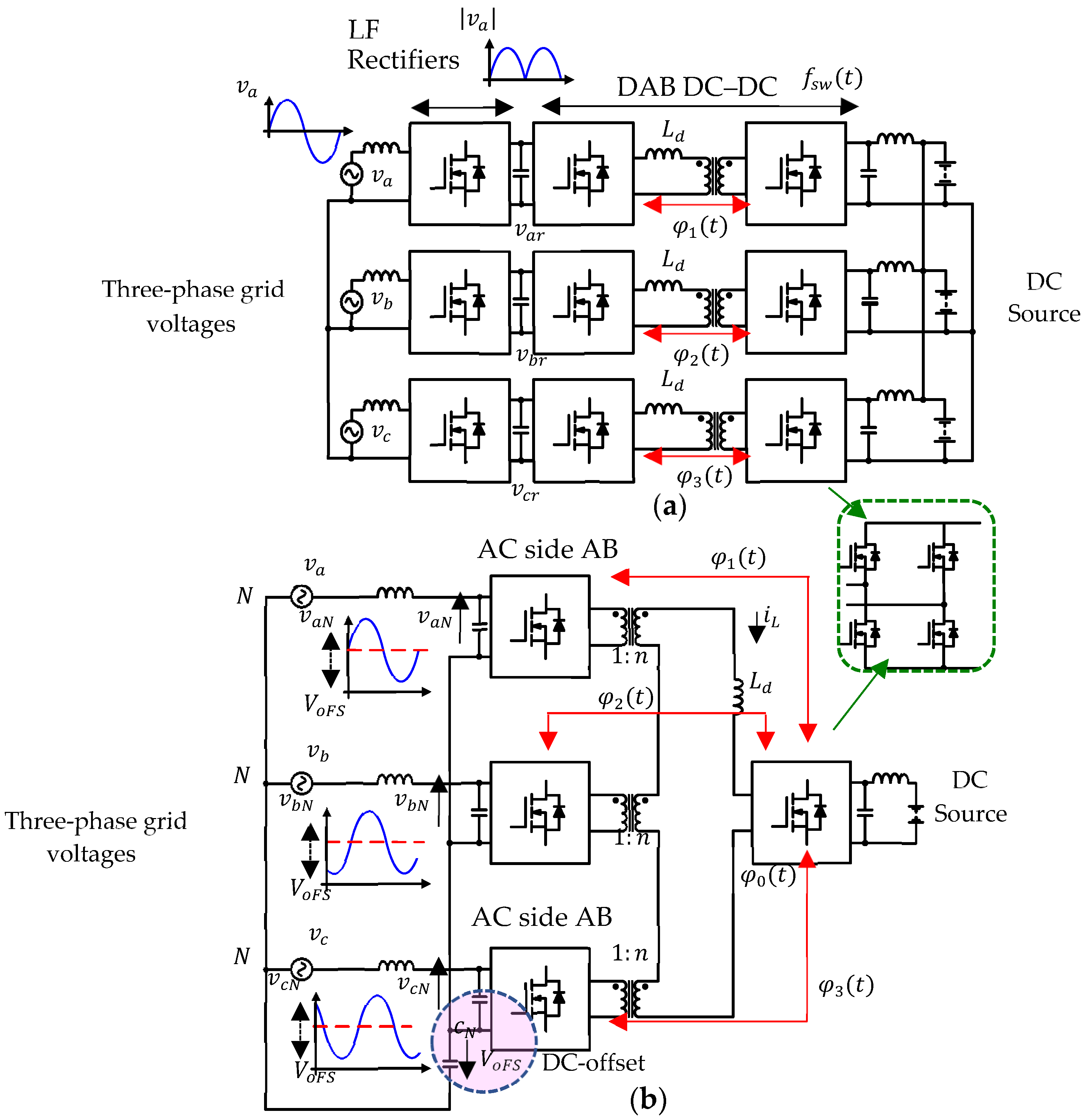
Figure 1. (a) Three single-phase DAB AC–DC converter [31], (b) three-phase QAB AC–DC converter with series-connected HF transformers [32].
Energies 15 08070 g001
Figure 2. The proposed SSIB three-phase AC–DC: three low-frequency rectifiers cascaded with a QABSR DC–DC converter.
Energies 15 08070 g002
Figure 3. Proposed modulation without reactive power injection ( θ = 0 ). (a) Grid voltages and currents, (b) rectified grid voltage and current, (c) HF modulated voltages at ω g t = π 2 .
Energies 15 08070 g003
Figure 4. Proposed modulation with reactive power injection ( θ = π 6 ). (a) Grid voltages and currents, (b) rectified grid voltage and current, (c) HF modulated voltages at ω g t = π 2 .
Energies 15 08070 g004
Figure 5. Working principle of the proposed SSIB three-phase AC–DC.
Energies 15 08070 g005
Figure 6. Steady-state analysis with the equivalent tank circuit.
Energies 15 08070 g006
Figure 7. Equivalent DABSR DC–DC converter of the proposed QABSR DC–DC converter.
Energies 15 08070 g007
Figure 8. Modulated voltages and the SRC current for G2V power flow.
Energies 15 08070 g008
Figure 9. Average model for the grid current. (a) With LF rectifier, (b) without LF rectifier.
Energies 15 08070 g009
Figure 10. Closed-loop control strategy for the proposed converter.
Energies 15 08070 g010
Figure 11. Bode plot analysis. (a) Average model transfer function G i ( s ) . (b) Open-loop response for the proposed controller: P I ( s ) L P F ( s ) G i ( s ) . (c) Closed-loop response of the system.
Energies 15 08070 g011
Figure 12. The experimental setup for the 2 kW prototype.
Energies 15 08070 g012
Figure 13. G2V power flow test for 2000 W.
Energies 15 08070 g013
Figure 14. V2G power flow test for −1500 W.
Energies 15 08070 g014
Figure 15. Modulated grid voltages and HF current for 2 kW G2V test.
Energies 15 08070 g015
Figure 16. ZVS analysis for 2 kW G2V at ω g t = α a 2 = π 2 and α o 2 = π 2 .
Energies 15 08070 g016
Figure 17. ZVS analysis at 2 kW for G2V at ω g t = α a 2 = π 6 and α o 2 = π 2 .
Energies 15 08070 g017
Figure 18. ZVS analysis for −1500 W V2G at ω g t = α a 2 = π 6 and α o 2 = π 2 .
Energies 15 08070 g018
Figure 19. Reactive power compensation. Analysis for two different S : (a) HF current amplitude I L analysis considering a constant S = 1.8 kVA ; (b) HF current amplitude I L analysis considering a constant S = 1.5 kVA .
Energies 15 08070 g019
Figure 20. Inductive RPC for S = 1.8 kVA, PFA θ = 30 ° and α o 2 = 60 ° .
Energies 15 08070 g020
Figure 21. Capacitive RPC for S = 1.5 kVA, PFA θ = 80 ° and α o 2 = 42 ° .
Energies 15 08070 g021
Figure 22. HF current for S = 1.8   kVA , at ω g t = α a 2 60 ° and α o 2 60 ° .
Energies 15 08070 g022
Figure 23. HF current for S = 1.5   kVA at ω g t = α a 2 30 ° and α o 2 42 ° .
Energies 15 08070 g023
Figure 24. THDi analysis for different power in G2B power flow.
Energies 15 08070 g024
Figure 25. Efficiency analysis for the QABSR converter.
Energies 15 08070 g025
Figure 26. Losses distribution at 2000 W B2G power flow.
Energies 15 08070 g026
Figure 27. Steady-state response for unbalanced grid conditions at 2 kW G2B: (a) DC output current for unbalanced grid voltages ( a = 0.7 ) ; (b) grid currents for unbalanced grid voltages ( a = 0.7 ).
Energies 15 08070 g027
Figure 28. HF current amplitude I L for different voltage drops: a = 0 , a = 0.1 and a = 1 , considering active power injection P o = 2   kW .
Energies 15 08070 g028
Figure 29. HF current amplitude I L for different voltage drops: a = 0 , a = 0.1 and a = 1 , considering active power injection P o = 500   W .
Energies 15 08070 g029
Table 1. DC/AC converter design parameters.
ParameterValue
Converter   Power   P o 2 kW
Grid   amplitude   ( phase - neutral ) :   V m 220 2 V , 60 Hz, 3Ø
Output   voltage   V o 400 V
Switching   frequency   f s 120 kHz
Quality   Factor   Q 4
Frequency   Ratio   F = ω s ω r = 2 π f s 2 π f r 1.1
Table 2. DC/AC converter parameters.
ParameterValue
Converter Power S o ,   P o 2 kVA, 2 kW
Grid amplitude (phase-neutral), frequency: V m ,   f g 220 2 V , 60 Hz, 3Ø
Output voltage V o 400 V
Switching frequency120 kHz
Quality Factor Q 4.1
Frequency Ratio F = f s f r 1.1
Resonant Inductor L r 390 µH
Resonant Capacitor C r 5.5 nF
Turns ratio n 0.86
AC filter Inductor L i 200 µH
AC filter capacitor C i 1 µF
Damping resistor1.1 Ω
QAB SiC MOSFETC3M0065090
Table 3. Comparison with similar single-stage DC–AC converters.
ParametersProposed ConverterSSIB [29]SSIB [30]
Structure3 LF rectifiers cascaded
with a QABSR DC–DC
3 LF rectifiers cascaded
with 3 DABs DC–DC
QAB AC–DC converter
(with DC OFFSET)
Storage Element1 SRC3 HF inductors1 HF inductor
Modulation3 Time-variant DR angles with one fixed
phase-shift angle
3 Time-variant
phase-shift angles
3 Time-variant
phase-shift angles
Switching frequencyFixedTime-variantFixed
Control complexityLowHighHigh
Power densityMediumHighMedium
( C r cap) ( C o f s cap)
THD2.9%6%4.5%
Capability for V2GActive–reactive power
reported
Only active power
reported
Only active power
reported
Table 4. Comparison with two-stage AC–DC converters.
ParametersProposed ConverterTwo-Stage 2L DC–AC
Converter for SST [39]
Two-Stage 2L DC–AC
Converter for SBC [8]
Film Cap.Electrolytic Cap.Electrolytic Cap.
DC link v d c 198 V(400 V)(800 V)
CapacitorTinyBulkyBulky
DurabilityHighLowLow
L FilterSmallBulkyBulky
MOSFET
Quantity
282814
Switching
Mode
3 - 1 ϕ Rectifiers
(LF and ZVS)
QABSR
(HF and ZVS)
3 - 1 ϕ VSI
(HF and HS)
QAB
(HF and ZVS)
1 - 3 ϕ VSI
(HF and HS)
DAB
(HF and ZVS)
Publisher’s Note: MDPI stays neutral with regard to jurisdictional claims in published maps and institutional affiliations.