Abstract
This article proposes the study, control and analysis of the topology of an AC–AC modular multilevel converter, known in the literature as the Hexverter. The Hexverter is capable of converting the energy between two AC systems with a reduced number of elements, if compared with other modular multilevel topologies, which makes this topology attractive in AC–AC applications. However, there are few studies about the Hexverter in the literature, so this work presents its operation principle, conducts modeling, and proposes a control scheme for the converter’s proper operation, validating the operation and control via hardware-in-the-loop emulation.
1. Introduction
One of the main industrial applications for static converters is the electrical drive for variable speed motor control. Typically in these applications, the conversion is performed in two stages. The energy from the electrical grid, considering the fixed voltage and frequency, is rectified to a regulated DC bus, and in the second stage, the DC bus voltage is converted to a three-phase system with variable voltage and frequency that controls the driven machine, regulating its torque and speed [1,2,3,4,5].
This AC–DC–AC conversion is widespread in the literature and is widely employed in industry, being generally employed for converters in the back-to-back configuration. This solution for AC–AC energy conversion is very robust; however, a DC bus with high voltage levels is required, employing electrolytic capacitors, which are bulky components with a high failure rate and a short service life [6].
The AC–AC conversion may also be achieved by a direct converter, i.e., without an intermediate energy storage stage. Among the direct converters, the matrix converters [7] stand out, which present high power density once capacitors are not employed in these topologies. However matrix converters can only be employed in applications where the output voltage is lower than the input voltage, and the lack of capacitors makes the converter control more complex. Once the converter dynamics are more susceptible to parametric variations, the switches actuation must be accurate to prevent short circuits or opening of an inductive circuit [8,9].
Another application for direct frequency converters that has become more popular in recent decades is the real-time emulation, PHIL (power hardware-in-the-loop) [10,11,12], whereby the converter can emulate loads, such as linear loads, non-linear loads, or electric motors. At the same time, it regenerates the energy to the electric grid, allowing these converters to be employed for the development and testing of electrical and electronic equipment such as electronic converters, motor drives, and protection systems, in addition to enabling tests on more complex systems that could not be tested in any other way, such as transmission lines, power systems, and micro-grids. Studies show that PHIL emulation presents better results than numerical simulations [12].
In recent decades, modular multilevel converters have been widely studied and are beginning to be employed in medium voltage applications, such as rectifiers, active filters, and motor drives. More recently, different MMC topologies have been proposed, mainly in three-phase AC–AC conversion [13].
The main MMC AC–AC topologies are the indirect MMC converter (back-to-back topology), the direct matrix converter (M3C), and the Hexverter. Other topologies have also been proposed, such as in [14], where the Hex-Y topology is proposed, being a combination of different MMC, aiming to combine the different advantages of each converter.
A more recent work [15] proposes modeling and control in a unified two-frequency dq framework and develops a virtual to achieve converter power balance. At the same time, it evaluates two modulation strategies (nearest level control and phase-disposition), validating the results via simulation.
This paper presents the analysis and modeling of the Hexverted, an AC–AC modular multilevel converter, and proposes a control strategy that allows the conversion between two three-phase electrical systems with different levels of voltage, currents. and frequency.
Employing the synchronous and stationary reference frame, the converter current and voltage transfer function can be obtained, which allows classical control theory to be employed for the controller’s design, resulting in simpler control for implementation and providing regulation with a proper transient response.
The control strategy is experimentally validated by employing hardware-in-the-loop emulation.
2. The Hexverter Modular Multilevel Converter
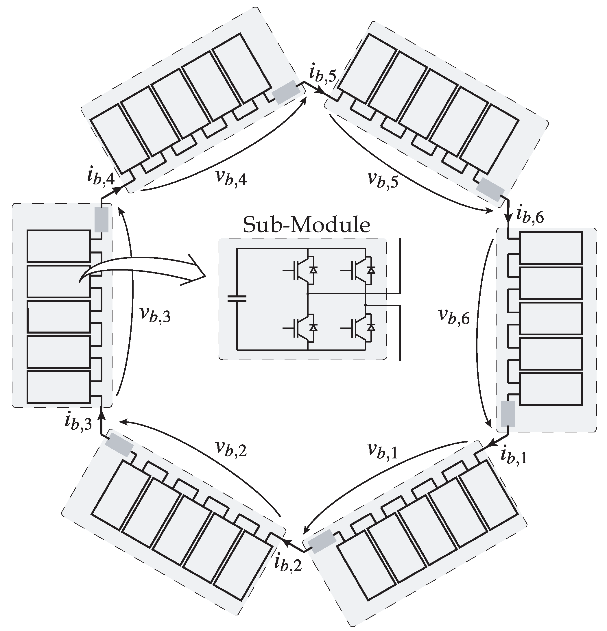
The Hexverter topology, as presented in Figure 1, consists of six arms connected to each other in the shape of a hexagon, hence the name Hexverter (hexagonal converter) [16].
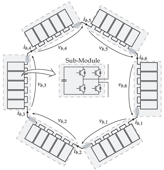
Figure 1.
Hexverter topology depicting the connections between the six arms and the sub-module’s H-bridge topology.
Similar to other modular multilevel converters, the Hexverter’s arms consist of an inductor, to limit the circulating current, and n sub-modules that impose the arm’s voltage, controlling the power flow between the two AC systems.
It is important to note that the sub-modules of the Hexverter must operate in four quadrants (bidirectional in current and voltage) since it is an AC–AC converter. As depicted in Figure 1, the H-bridge converter is employed for the sub-modules.
The AC systems are designated as port 1 (P1—relative to the phases A, B, and C) and port 2 (P2—relative to the phases R, S, and T), as the input port and output port, respectively. P1 and P2 can have different electrical characteristics of frequency, phase, reactive power, voltage, and current amplitude.
Hexverter Operation Principle
Assuming that the converter is operating properly, it can also be assumed that port P1 is composed of the phases A, B, and C, and port P2 is composed of the phases R, S, and T. The following equations describe the voltages and currents:
Considering the port voltages applied to the converter and the currents drained/injected into the ports and neglecting the voltage drop in the arm inductor, the voltages in the two adjacent arms are roughly equal to the line voltage applied by the respective port, while the current that circulates in each arm is equal to the phase current.
This results in the arm’s voltages being given by:
Furthermore, the arm currents are given by:
It can be noted that each converter’s arm has voltage and current components from both ports, given by the phase current and voltage, which implies an additional 30° lag between arm voltage and current components from the same port.
3. Hexverter Modeling
For modeling the Hexverter, the quasi-instantaneous average model of the converter will be considered, as presented in Figure 2, where the n sub-modules of the converter are substituted by their equivalent circuit.
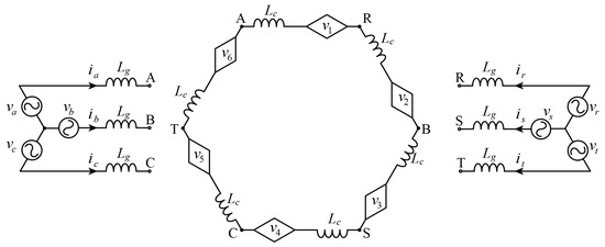
Figure 2.
Equivalent circuit of the Hexverter, where the sub-modules are replaced by the equivalent model of a voltage source on the AC side and a current source on the DC side.
The converter model is obtained in a synchronous reference frame for the current control of the port and in stationary reference frame for the DC bus voltage control of the sub-module.
3.1. Synchronous and Stationary Reference Frame Transformation
Here, we present the transformations employed for converter modeling and control. The synchronous reference frame (dq0 transformation) and stationary reference frame ( transformation) are considered.
The synchronous voltage transformation (dq0 reference frame) is given by
where it can be seen that the stationary reference frame transformation is multiplied by the rotation matrix. Similarly, the synchronous transformation for the converter currents can be given as follows:
It can be seen that the voltage and the current are different. This is due to the converter geometry and the currents and voltages on each of the converter’s arms.
Although both transformations are power-invariant, they are not orthonormal, which implies that the inverse transformation is not equal to the transpose. However, the inverse voltage transform is equivalent to the transpose of the current transformation. Similarly, the current inverse transformation is equal to the voltage transformation transpose.
Another important observation is that applying the power invariant dq0 transformation to the ports’ voltages and currents results in the same direct and quadrature components as those calculated by Equations (19) and (20).
For the arms’ DC buses, the following transformation can be considered:
The arms’ DC bus transformation aims to decouple the influence of each arm’s current and voltage from the bus voltage. This will become more apparent later, when the DC bus voltage equations are presented.
3.2. Input Current Model and Transfer Function
By equating the converter equivalent circuit depicted in Figure 2, it is possible to obtain the following matrix equation, which describes the current in the Hexverter’s arms.
Applying the voltage and current dq transformation, it is possible to obtain the input current equations in dq coordinates for the converter, which are described by the matrix equation as
From the input current equation, it is possible to obtain the equivalent circuit in dq coordinates, as shown in Figure 3.
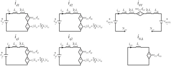
Figure 3.
Equivalent circuit for the converter currents in dq coordinates.
It is possible to observe that, with the synchronous transformation, four equivalent circuits were obtained for the differential components of the currents, wherein the components from P1 are independent of the P2 components.
In addition, the model is similar to other three-phase AC converters, which allows the same control strategies to be employed for the input currents, which are already well-described in the literature.
The other two circuits control the common mode currents. The will only circulate if the two ports’ neutral points are connected, and the is the converter circulating current.
3.3. DC Bus Voltage Model and Transfer Function
To obtain the stationary reference frame equivalent model and subsequently the transfer function for the DC bus voltage, the same procedure is adopted as the one for obtaining the input current model, being equated with the DC bus voltages as:
By pre-multiplying the equation by the DC bus voltage transformation presented in Equation (24) and substituting the duty cycle and current values by the components in the stationary reference frame, it is possible to obtain the equation for the equivalent DC buses in the stationary reference frame.
Some of the DC bus current components are neglected because they do not influence the average bus voltage. This occurs with components that are the products of the current and duty cycle between port 1 and port 2 (, , , , , , , and ) since they have different frequencies, the average value is equal to zero, and they only contribute to the DC oscillating voltage.
Furthermore, the is null since there is no connection between the two systems’ neutral point, so this component of the DC bus current may be neglected. Considering this simplification, it is possible to obtain the following equations for the DC bus voltages:
Note that the currents in port 2 are imposed by the control, and the currents in port 1 must be regulated so the active power in both ports is equal, discounting the converter losses. By ensuring this, it is possible to regulate the total voltage ().
Considering this, the only variables left to regulate the other five DC voltages components are the circulating current () and the common mode voltage imposed by the converter with the duty cycle .
From the DC bus voltage equations, it is possible to define the following transfer functions for the control of the DC voltages:
It is important to note that the circulating current () is responsible for controlling all five differential DC voltage components (, , , , and ). To achieve this for each differential DC voltage component, the control must impose a circulating current in the same frequency and in phase with its relative voltage; for example, to control the , the circulating current must have a component in phase with the voltage .
In Equation (29), it can be seen that the is dependent on the reactive power in both ports of the converter, which means that the reactive power being processed in each port will directly influence the balance of the DC buses. In other words, if the Hexverter operates with reactive power, it will cause an imbalance in the DC buses that will need to be compensated for.
4. Control
In this paper, the Hexverter is considered to be connected with two three-phase voltage sources, with different characteristics in terms of voltage and frequency. This occurs in applications such as the connection of two electrical grids or the connection of generators with mains, mostly in the field of wind generation.
It is essential to note that the converter can also operate by controlling the output port (P2) voltage if it is feeding a load, when the voltage is not imposed in the converter port by an external source.
The converter has two main control loops, a faster internal loop that controls the currents and an external slower loop that controls the DC bus sub-module voltages. Furthermore, a power loop that generates the current reference for one port must be considered, for instance, an MPPT algorithm for a wind generator or a power-flow reference (active and reactive power) for the connection between two electrical grids.
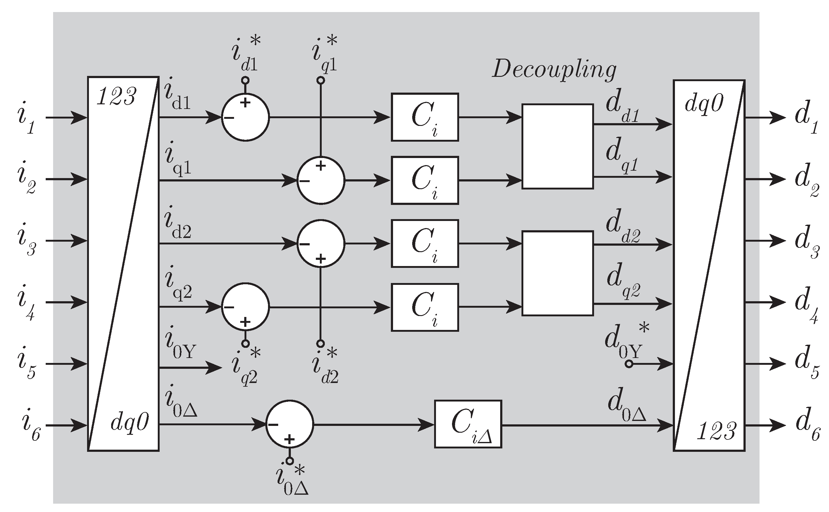
4.1. Current Control Loop
The current control loop is responsible for imposing the currents in the ports and the circulating current in the converter (). It can be observed that there is no connection between the two system neutrals, which implies that the current is always null since there is no path to its flows.
For the ports, the control in dq coordinates is considered similar to any three-phase converter where the current error is applied to a controller—a PI controller in this case. Afterward, the decoupling is applied to the PI output, generating the reference for the converter modulator.
To control the circulation, a PI controller is employed, the input being the current reference subtracted from the measured, and the output being the duty cycle . Figure 4 depicts the control block diagram.
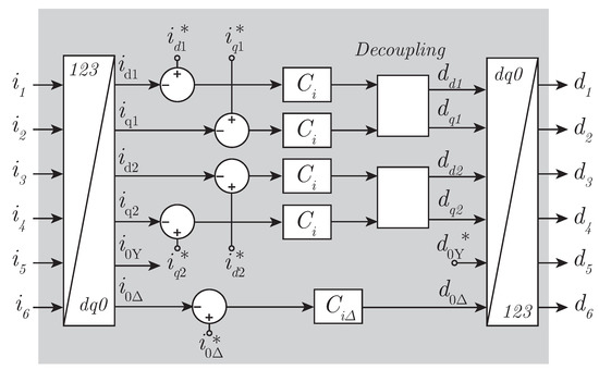
Figure 4.
Current control scheme for the Hexverter.
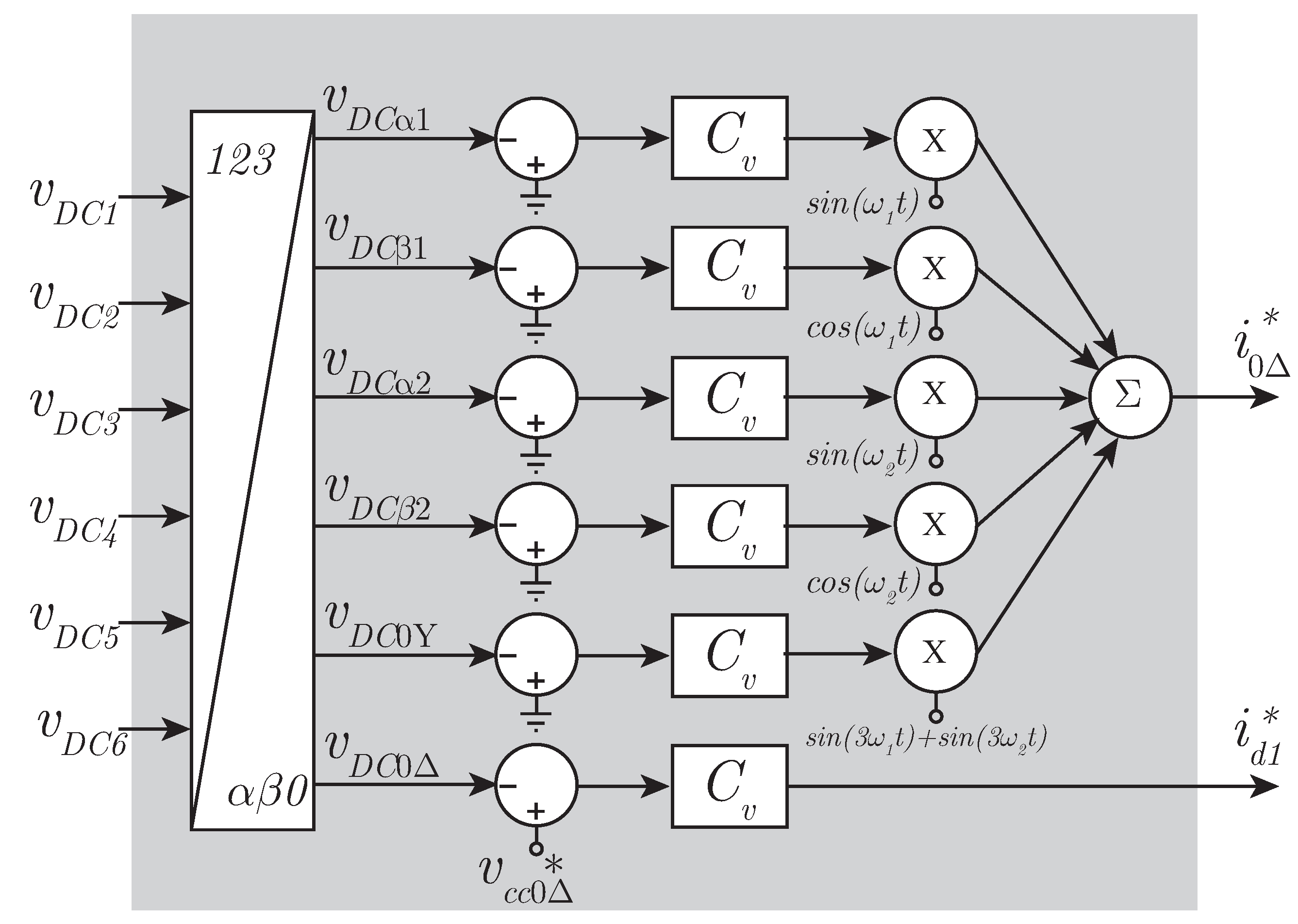
4.2. Voltage Control Loop
The voltage control loop regulates the voltages in the sub-module’s DC buses, generating the current reference for port 1 and the circulating current (). In this work, the current reference for port 2, generated by the power flow reference algorithm, is already considered to be known, so these currents are regulated by considering an imposed reference.
As previously stated, the voltage is controlled by the P1 currents and , being related to the active power and being related to the reactive power.
The is controlled by imposing a value of voltage. In this work, the imposed is equal to ; this reduces the peak amplitude of the voltage imposed by each converter arm allowing the DC bus voltage usage to be maximized. The effective control of the is achieved by controlling the circulating current .
The remaining differential components of the DC bus voltage are controlled by adding alternating components to the circulating current . Ideally, the current’s components should be in phase with the voltage imposed by the converter; however, considering that the phase shift between the converter and the load/feed is typically low, it is possible to synchronize it with the ports’ voltage considering a small loss of performance.
The DC bus voltage control is presented in Figure 5, where it can be observed that this control loop generates the references for the and currents.

Figure 5.
Voltage control scheme for the Hexverter.
4.3. Converter Parameters and Control Design
For the proper operation of the converter, a suitable design of the converter parameters (inductances and capacitances) and the controllers is required. Here, we present the design guidelines employed in this work.
To calculate an appropriate value of grid inductance, the power flow equation between two buses with a inductive transmission line is considered, which results in the following equation:
Considering that the grid voltage () is approximately equal to the voltage imposed by the converter () and assuming a small value for the lag (smaller than 5°), it is possible to calculate the grid inductance with the converter power and the frequency of operation.
The adopted circulating inductance () is 10% of the grid inductance.
In order to calculate the sub-module’s capacitance, the oscillating power in the arm is considered, which results in the following equation to calculate the sub-module capacitance with the desired voltage ripple:
This equation considers the converter operating with the unit power factor in both ports; thus, only the ripple from the double frequency of each port is considered. However, when the converter operates with reactive power, an increase in the voltage ripple is observed, mainly in the frequency equal to the difference of the two ports’ frequency ().
With the current and voltage transfer function, it is possible to design the current loop control and voltage loop control, employing classical control theory to design the controllers.
It is important to consider that the most internal control loops (current control loops) must have a faster response than the external control loops (voltage control loops).
In this paper, the phase-shift modulation is considered, and the duty cycle generated by the current control is directly applied to the modulators that generate the pulse for each respective arm sub-module, with each sub-module from the same arm being shifted by 360 degrees divided by the number of sub-modules per arm .
5. Experimental Results
To obtain the experimental results for the Hexverter, the OPAL-RT OP-5700 was employed to emulate the converter. The HIL is responsible for emulating the Hexverter. The control was implemented in a Cyclone V FPGA, as seen in the control board. The control board samples the HIL’s analogs output and generates the PWM pulses to control the Hexverter, which is being emulated in the HIL. The emulation system is shown in Figure 6.
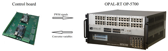
Figure 6.
A picture of the control board where the control strategy is implemented, and the HIL OPAL-RT OP-5700, which is responsible for the real-time converter emulation.
The emulated converter is considered to be connected to two grids with different frequencies, and the power flow is considered to be from port 1 to port 2. The converter parameters are depicted in Table 1.

Table 1.
Converter parameters specification.
Here, we present the experimental results obtained with the FPGA-based control board and the OPAL hardware-in-the-loop. The results considering the steady-state operation of the converter are presented first, and the transient response performance is presented last.
5.1. Steady-State Operation
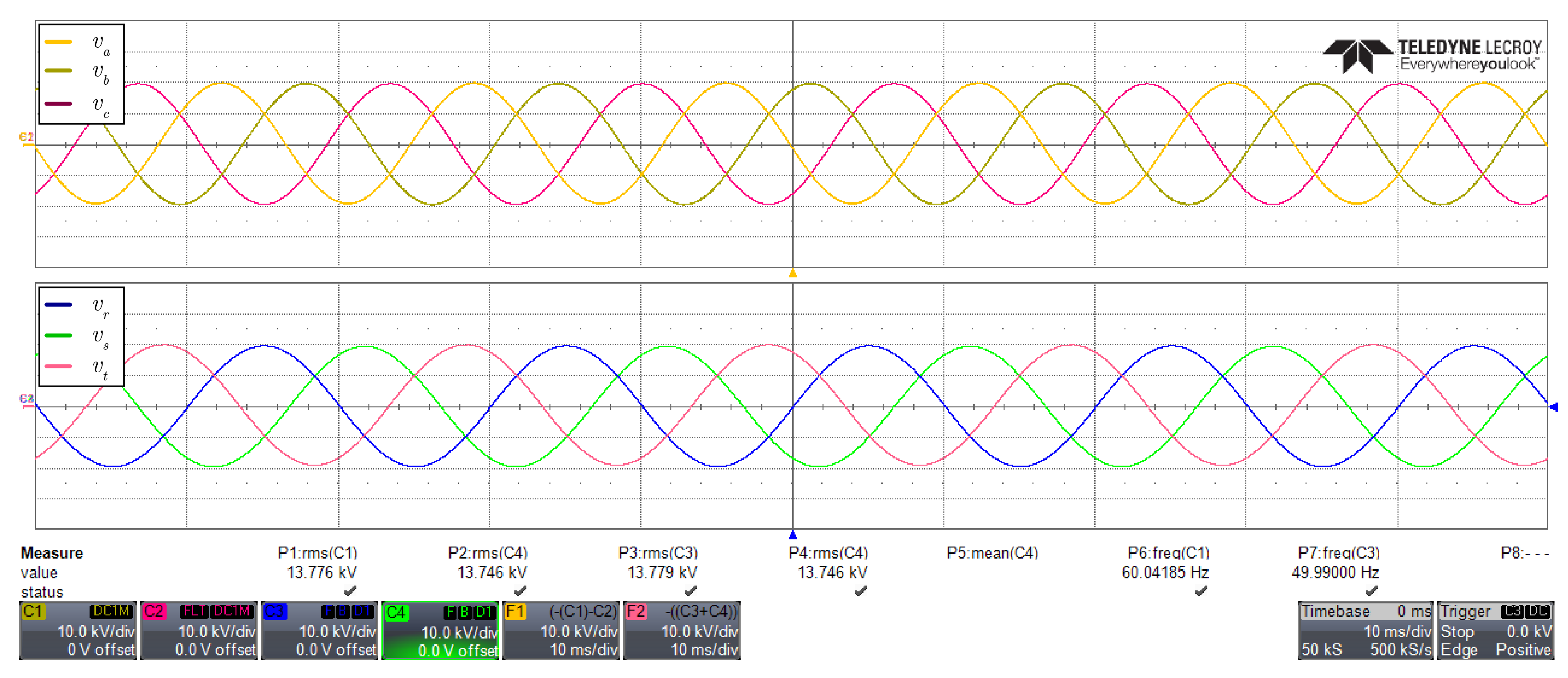
Figure 7 shows the voltages in the converter ports. It is possible to observe the three-phase voltages that are imposed in the Hexverter ports.
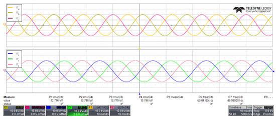
Figure 7.
Hexverter line voltages in both ports, where the 13.8 kV rms value is measured in both ports, with a frequency of 60 Hz in port 1 and 50 Hz in port 2.
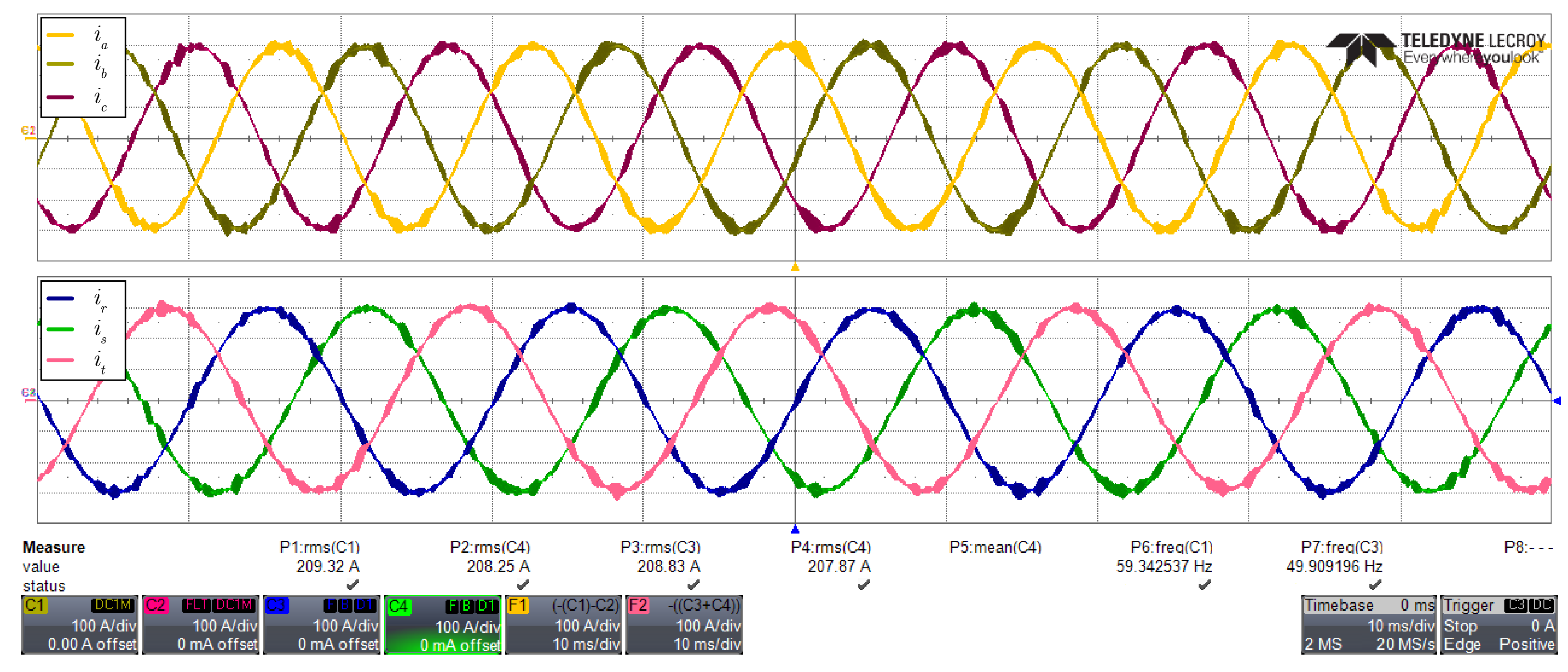
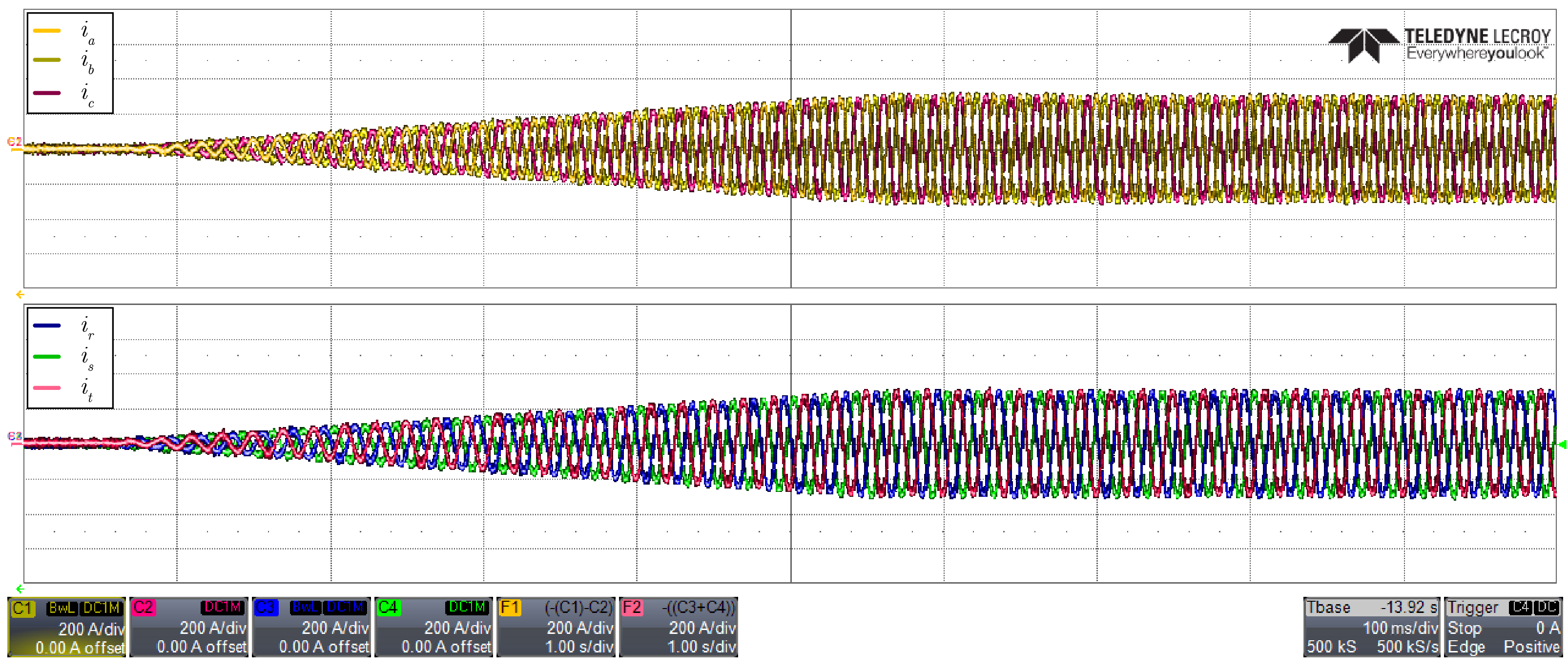
Figure 8 shows the currents in the converter ports. It is possible to observe the three-phase currents, which are regulated by the control, in the Hexverter ports.
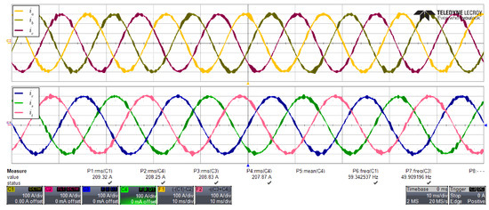
Figure 8.
Hexverter line currents in both ports, where the 209 A rms value is measured in both ports, with a frequency of 60 Hz in port 1 and 50 Hz in port 2.
The line currents in both ports can be observed, with a nominal value of 209 A and, consequently, a nominal power of 5 MW.
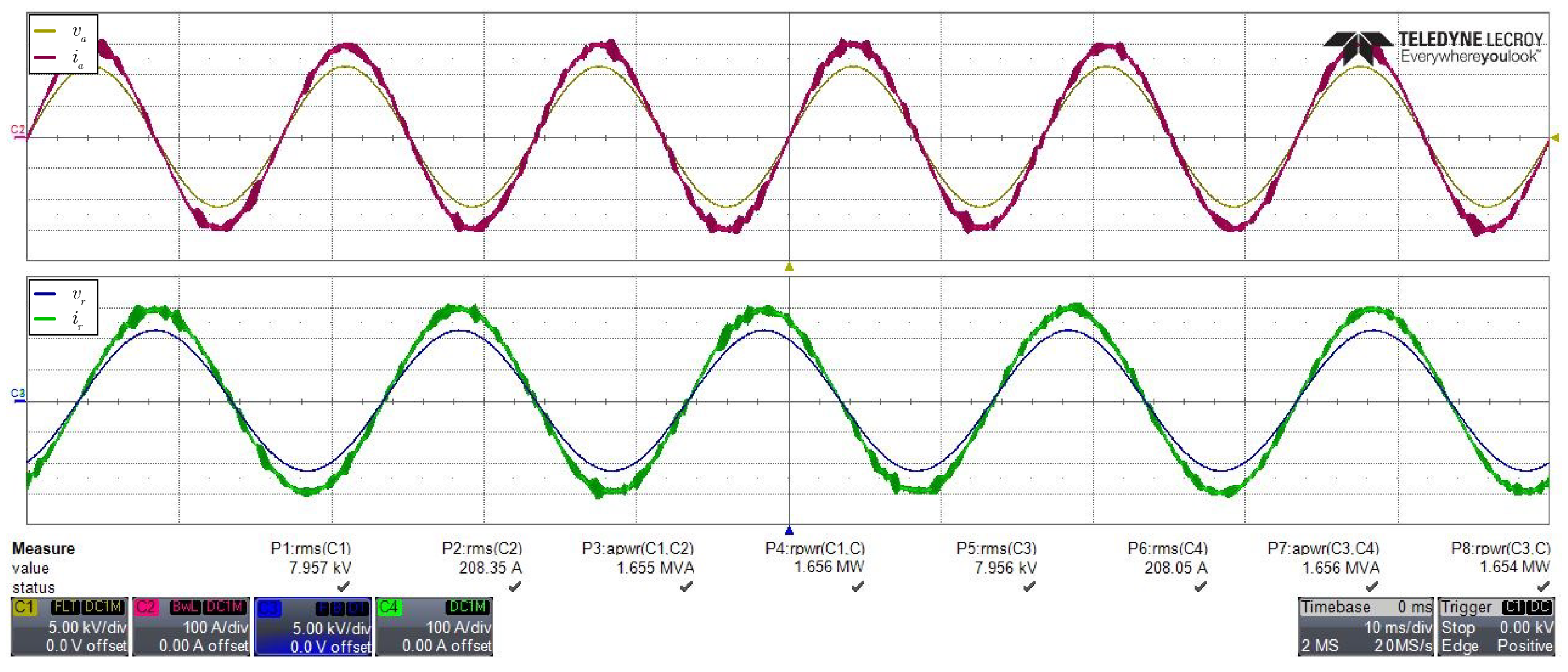
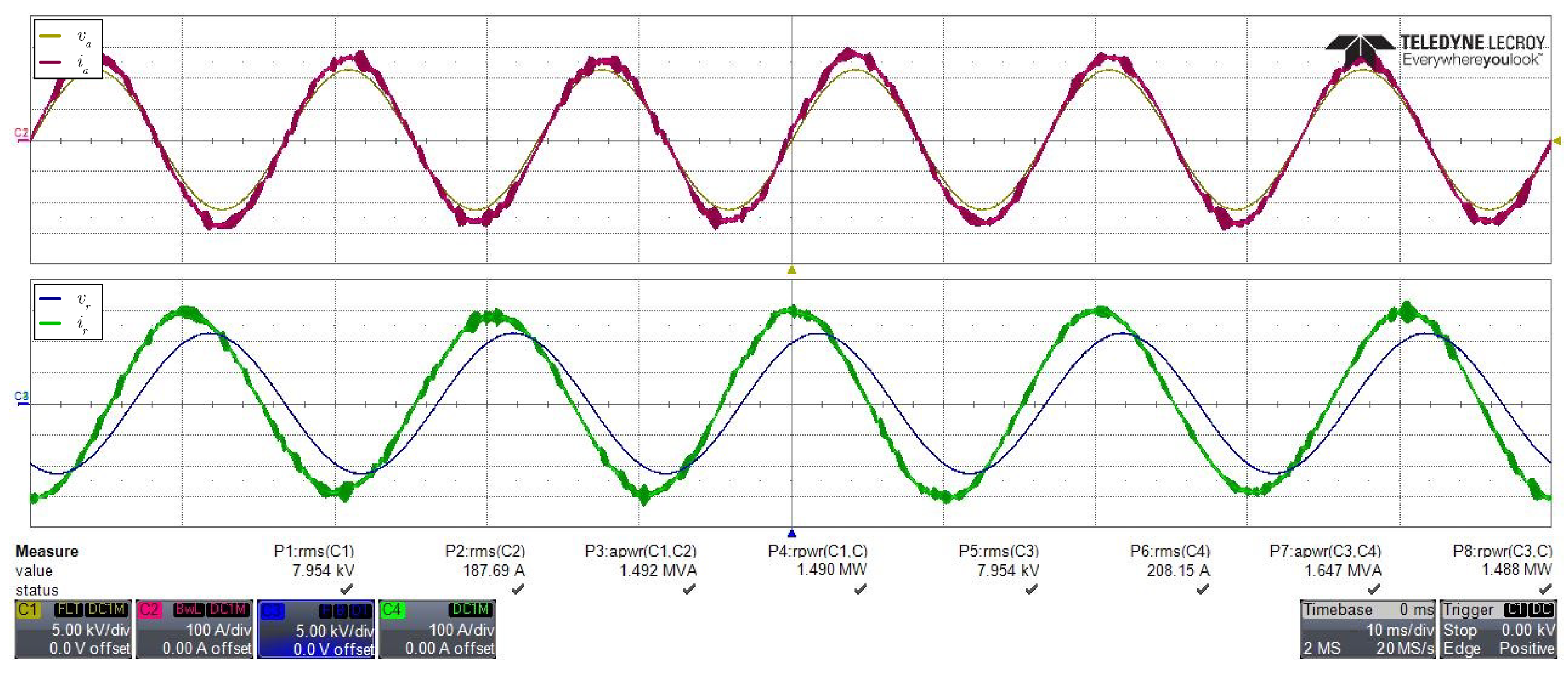
Figure 9 shows one voltage and one current value from each port of the converter, phase A from port 1 and phase R from port two. The active and apparent power per phase (calculated from the phase voltage and line current product) are shown.

Figure 9.
Converter operation with 5 MW power: phase voltage and line current in phase A port 1 and phase R port 2, showing the apparent and active power per phase in each port.
It can be seen that the converter operates with nominal power (5 MW or 1.66 MW per phase) and unit power factor in both ports, as evidenced by the apparent power being approximately equal to the active power.
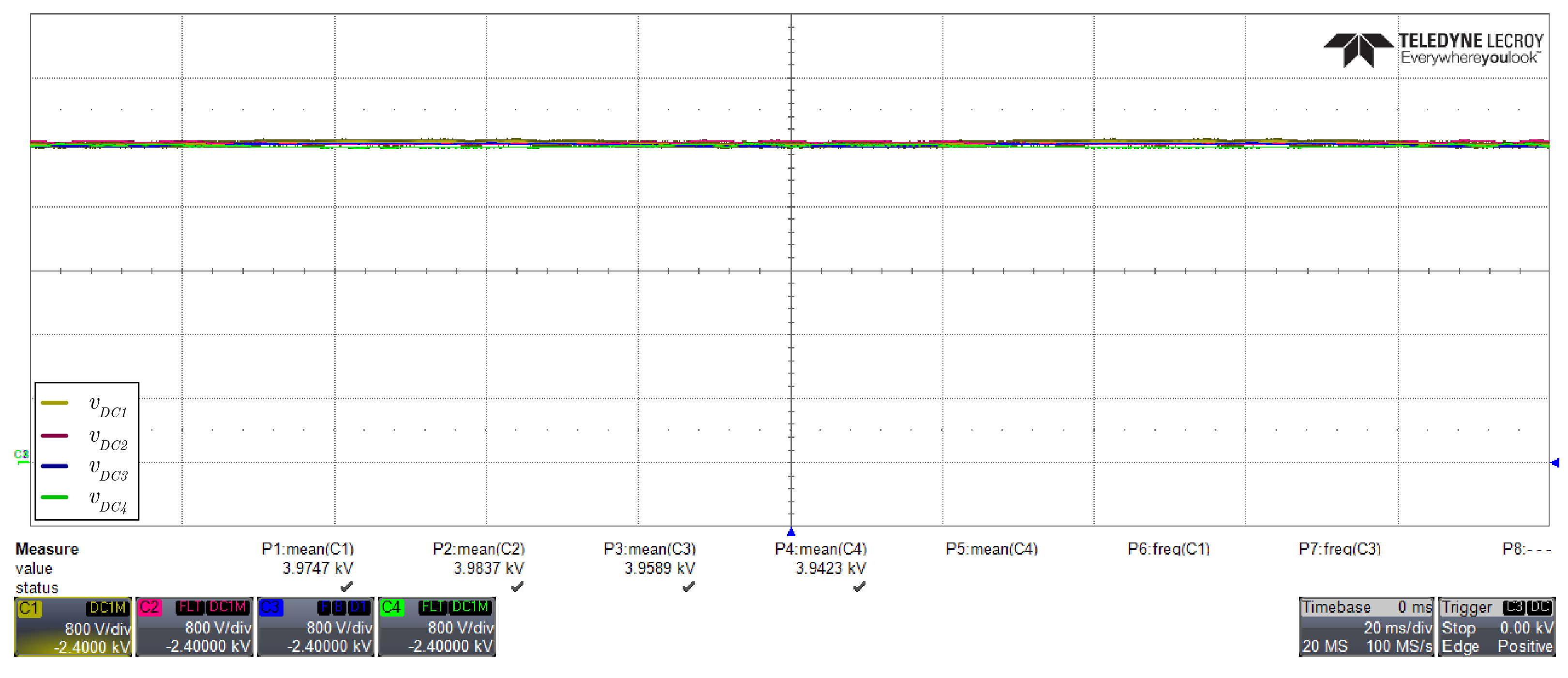
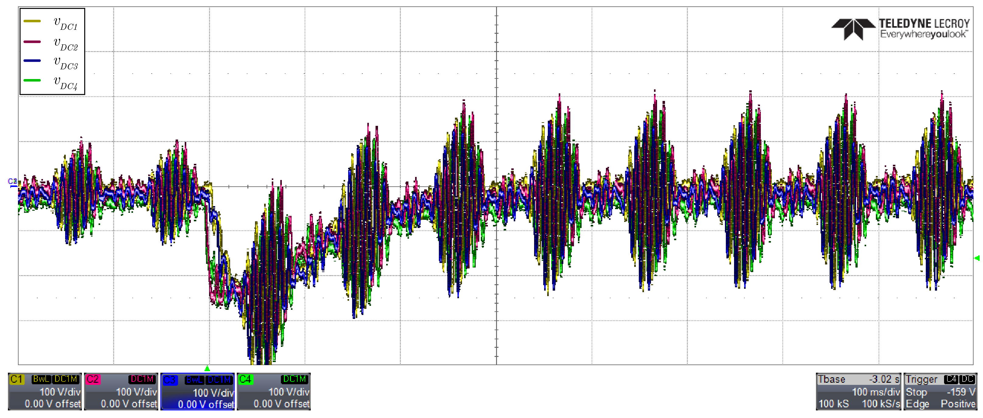
Figure 10 presents the DC bus voltage from four sub-modules from distinct converter arms. It can be observed that all the sub-modules have approximately the same average voltage (4 kV) and reduced ripple, as shown in detail in Figure 11.
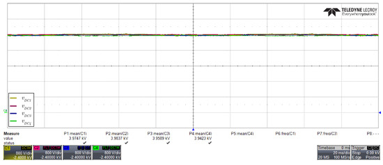
Figure 10.
Sub-module DC voltage from four different converter arms.
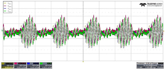
Figure 11.
Sub-module DC voltage ripple from four different converter arms, showing only the voltage alternating components.
The sub-module DC voltage ripple is relative to the single-phase power processed by the Hexverter’s arms, being basically composed by the frequencies , , , and .
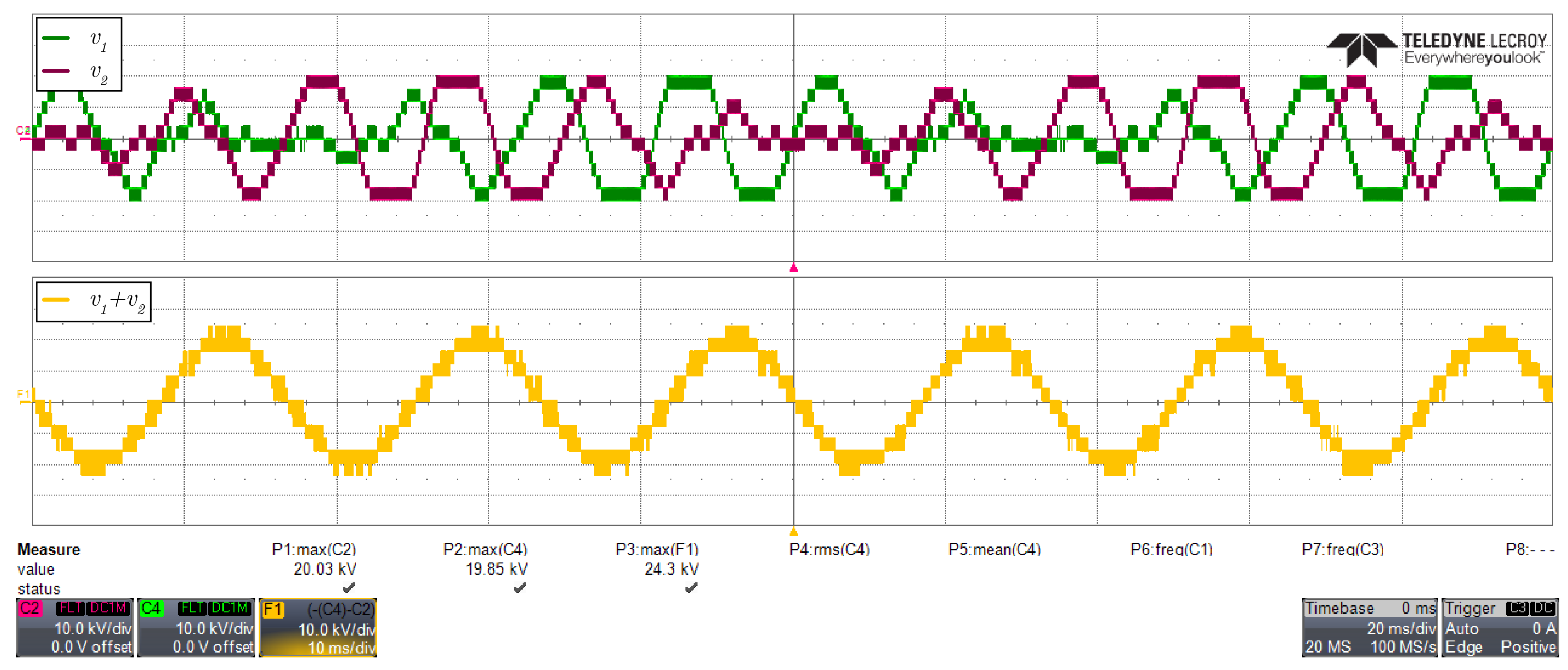
The synthesized arm voltages are presented in Figure 12, where the voltages of arm 1 and arm 2 are shown, as well as their sum, which is the line voltage.
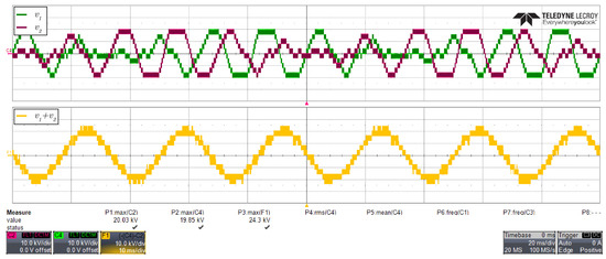
Figure 12.
Voltages synthesized by two adjacent Hexverter arms. The sum of both results in the line voltage imposed by the converter.
It can be noted that the maximum voltage imposed by the converter arm is equal to 5. This reduction of one level is achieved by the third harmonic injection in the modulation. Without the third harmonic, it would be necessary to use all six levels to achieve the peak voltage demanded to control the port’s currents.
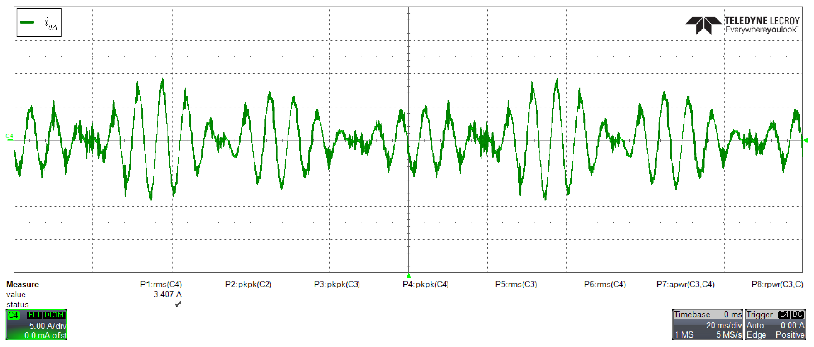
Figure 13 shows the Hexverter circulating current for the converter, operating with unit power factor in both ports. In this particular case, the circulating current is relatively small since the imbalance comes from the grid imbalance and deviation of the converter parameters due to the tolerance of the components.
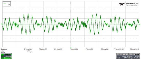
Figure 13.
Circulating current in the Hexverter, with the unity power factor in both ports.
In an operating situation with reactive power in one port, the circulating current would increase significantly. In this case, the current circulation in the converter could be reduced by increasing the common mode voltage level (third harmonic). However, to increase the common mode voltage, it would be necessary to increase the total DC bus voltage and eventually have more sub-modules per arm, leading to an over-dimensioned DC bus.
The operation with reactive power is presented in the following figures. It is considered a power factor of 0.9 in port 2, while port 1 operates with a unit power factor.
Figure 14 presents the voltage and currents from phase A (port 1) and phase R (port 2).
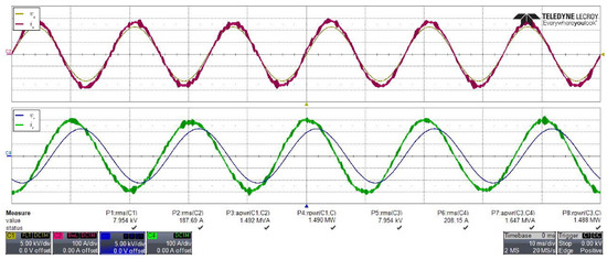
Figure 14.
Converter operation with 5 MVA apparent power in port 2 with cos() = 0.9, and port 1 with 4.5 MW and the unit power factor.
A leading current can be observed in phase R, while the current in phase A is in phase with the voltage.
In this case, as the converter processes reactive power, there is an imbalance in the common mode voltage (), which is compensated for by increasing the converter circulating current, as depicted in Figure 15.
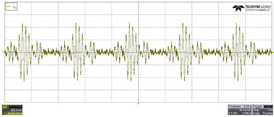
Figure 15.
Circulating current for the converter while processing reactive power.
As the common mode voltage is fixed to achieve the minimum DC bus voltage necessary to synthesize the line voltage, a significant increase is implied in the circulating current () to provide balance for the DC buses.
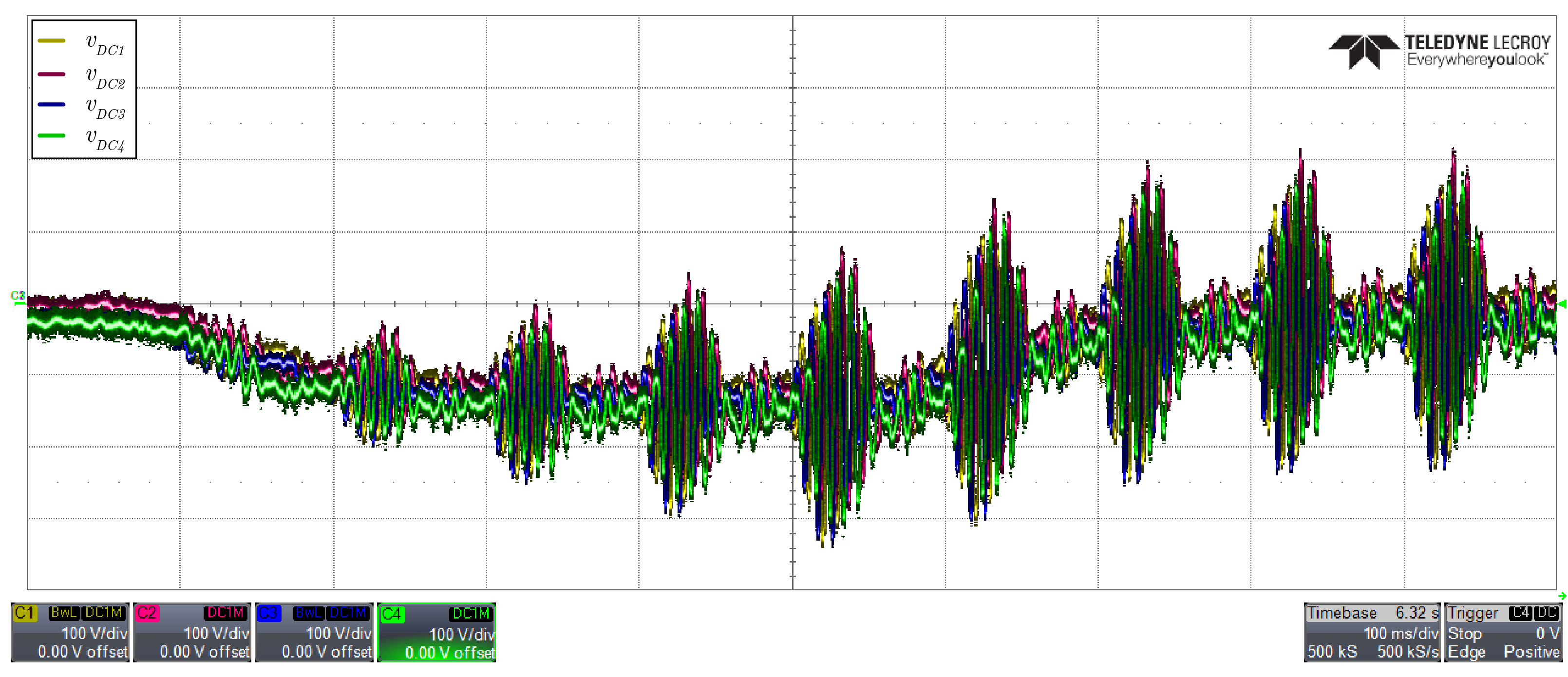
The processing of reactive power also increases the interaction between current and voltage from different ports, which increases the sub-module’s DC bus ripple, mainly in the frequency (), due to the increase in the oscillating power in this frequency in the arm, as shown in Figure 16.
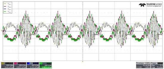
Figure 16.
DC voltages from four different sub-modules, considering the operation with reactive power.
5.2. Transient Response
The transient response of the converter to a step in the current reference in port 2 is presented in Figure 17. It can be seen that the converter can achieve a fast current transient response. At the same time, the voltage loop has a slower response.
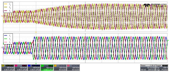
Figure 17.
Transient response showing the port currents for a step from 50% to 100% in the power injected in port 2 of the converter.
Figure 18 shows the DC voltages from the converter arms, without the average component.
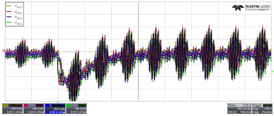
Figure 18.
Transient response showing the DC bus voltages for a step from 50% to 100% in the power injected in the port 2 of the converter.
It can be observed that the voltage is maintained after the transient response. It can also be observed that the ripple increases with the increase in power processed by the converter.
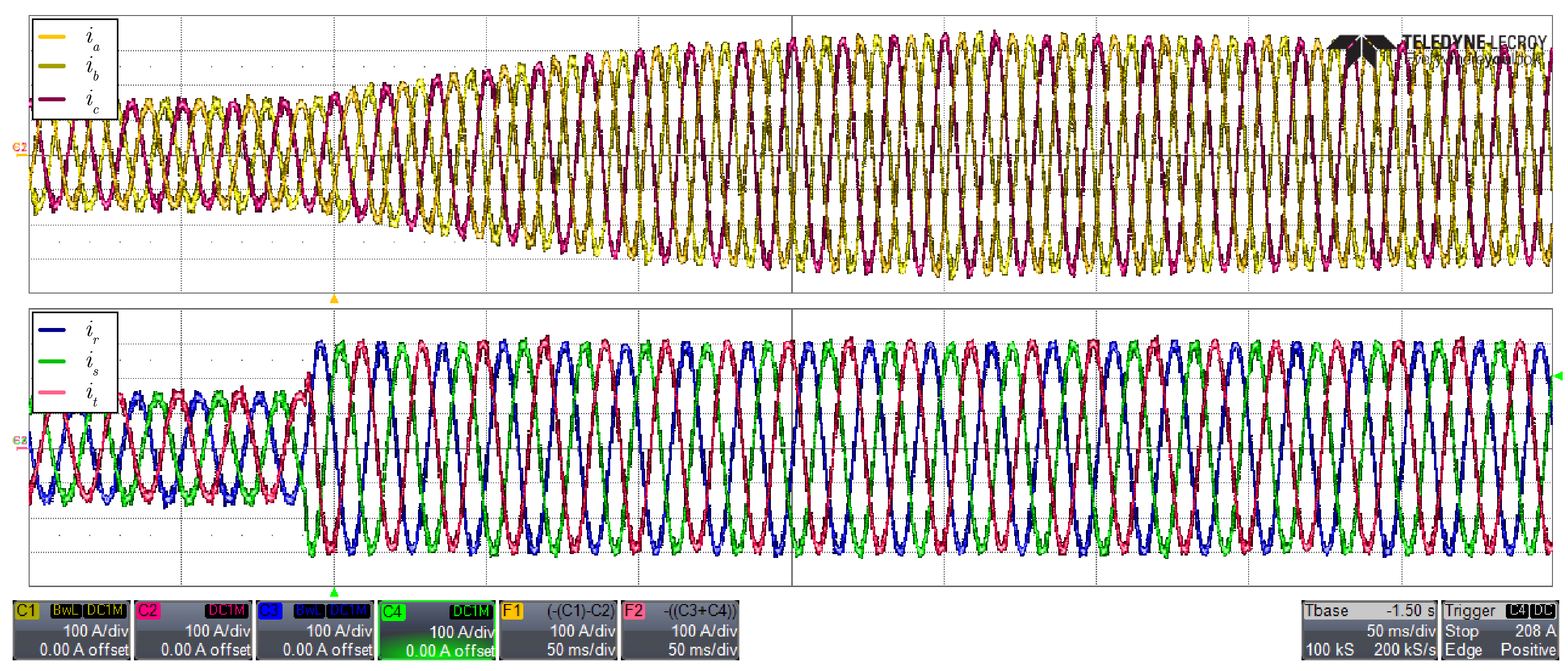
In addition, the control transient response was observed for the converter soft start with a ramp response for port 2. Figure 19 shows the transient response of the port 1 and port 2 currents for the ramp response range from 0% to 100% of power injected into port 2.
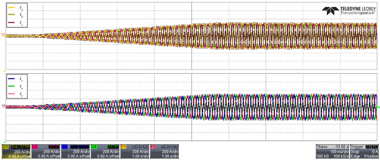
Figure 19.
Transient response showing the port currents for a ramp from 0% to 100% of power injected into port 2 of the converter.
The DC bus voltages for the ramp transient response are presented in Figure 20.

Figure 20.
Transient response showing the arms DC voltages for a ramp from 0% to 100% of power injected into port 2 of the converter.
In this case, the sub-modules’ DC voltages present a source of constant error during the transient response, achieving voltage regulation after the current in the port reaches its nominal value.
6. Conclusions
This paper presents a modular multilevel AC–AC converter modeled in a synchronous reference frame. The converter transfer functions were obtained, and a control scheme was proposed by employing classic control techniques.
A control strategy was proposed that regulates the currents in both converter ports as well as the circulating current and the DC sub-module bus. The control was validated by real-time emulation, employing the OP-5700 OPAL-RT real-time emulator, providing suitable results. The converter regulated the port currents with reduced harmonic distortion and also regulated the DC bus voltages.
As observed in the experimental results, the injection of the third harmonic allowed the DC bus usage to be maximized. This is an interesting aspect of the control, which allows the total DC bus voltage level to be reduced, or the converter redundancy to be increased, allowing the converter to operate with sub-modules.
On the other hand, choosing the third harmonic injection to be of the voltage amplitude implies the need for a high level of circulating current when the converter operates with different levels of reactive power between the two ports. This might be a limiting characteristic when using the converter in applications such as motor drives.
This could be observed when comparing the circulating currents of the converter operating with unit power factor in both powers (which presented a value of approximately 1% of the arm current). Meanwhile, when the converter operates by processing reactive power (cos() = 0.9), the circulating current increases to the same level as that of the converter line voltage.
The proposed control strategy is suitable for the operation of a converter with unit power factor in both ports; however, some modifications will eventually be necessary if operation with reactive power processing is considered. Increasing the third harmonic injection would represent a trade-off between the necessary bus voltage and the circulating current amplitude, depending on the reactive power that is processed by the converter.
The main contribution of this paper is the proposal and modeling of a simple Hexverter control strategy with a control scheme for the converter’s proper operation, allowing the design of controllers with classical control theory, which is widely known and is employed in various applications. The Hexverter is suitable in most high-power medium-voltage applications, such as wind power generation, medium-voltage motor drives, or connections between two electrical grids with different frequencies.
Author Contributions
Conceptualization, S.A.M. and M.L.H.; Formal analysis, C.A.A., S.A.M. and M.L.H.; Investigation, C.A.A. and M.L.H.; Methodology, C.A.A. and M.L.H.; Software, C.A.A.; Supervision, S.A.M. and M.L.H.; Writing—review & editing, S.A.M. and M.L.H. All authors have read and agreed to the published version of the manuscript.
Funding
The Graduate Program in Electrical Engineering (PPGEEL)—CAPES/PROEX: Code 41001010005P1.
Data Availability Statement
Not applicable.
Conflicts of Interest
The authors declare no conflict of interest.
References
- Jung, J.J.; Lee, H.J.; Sul, S.K. Control of the Modular Multilevel Converter for variable-speed drives. In Proceedings of the 2012 IEEE International Conference on Power Electronics, Drives and Energy Systems (PEDES), Bengaluru, India, 16–19 December 2012. [Google Scholar]
- Kucka, J.; Baruschka, L. A Hybrid Modular Multilevel DC/AC Converter. In Proceedings of the 17th European Conference on Power Electronics and Applications (EPE’15 ECCE-Europe), Geneva, Switzerland, 8–10 September 2015. [Google Scholar]
- Tai, B.; Gao, C.; Liu, X.; Chen, Z. A Novel Flexible Capacitor Voltage Control Strategy for Variable-Speed Drives with Modular Multilevel Converters. IEEE Trans. Power Electron. 2016, 8993, 128–141. [Google Scholar] [CrossRef]
- Marquardt, R. Modular Multilevel Converter topologies with DC-Short circuit current limitation. In Proceedings of the 8th International Conference on Power Electronics—ECCE Asia, Jeju, Korea, 30 May–3 June 2011. [Google Scholar]
- Alhasnawi, B.N.; Jasim, B.H.; Issa, W.; Esteban, M.D. A Novel Cooperative Controller for Inverters of Smart Hybrid AC/DC Microgrids. Appl. Sci. 2020, 10, 6120. [Google Scholar] [CrossRef]
- He, L.; Zhang, K.; Xiong, J.; Fan, S.; Xue, Y. Modular multilevel converter with full-bridge submodules and improved low-frequency ripple suppression for medium-voltage drives. In Proceedings of the 2015 IEEE Applied Power Electronics Conference and Exposition (APEC), Charlotte, NC, USA, 15–19 March 2015. [Google Scholar]
- Zhang, J.; Li, L.; Dorrell, D.G. Control and applications of direct matrix converters: A review. Chin. J. Electr. Eng. 2018, 4, 18–27. [Google Scholar]
- Belhaouane, M.M.; Ayari, M.; Guillaud, X.; Braiek, N.B. Robust Control Design of MMC-HVDC Systems Using Multivariable Optimal Guaranteed Cost Approach. IEEE Trans. Ind. Appl. 2019, 55, 2952–2963. [Google Scholar] [CrossRef]
- Baruschka, L.; Mertens, A. A new 3-phase direct modular multilevel converter. In Proceedings of the 2011 14th European Conference on Power Electronics and Applications, Birmingham, UK, 30 August–1 September 2011. [Google Scholar]
- Kolb, J.; Kammerer, F.; Schmitt, A.; Gommeringer, M.; Braun, M. The Modular Multilevel Converter as Universal High-Precision 3AC Voltage Source for Power Hardware-in-the-Loop Systems. In Proceedings of the PCIM Europe 2014, Nuremberg, Germany, 20–22 May 2014. [Google Scholar]
- Schmitt, A.; Gommeringer, M.; Rollb, C.; Pomnitz, P.; Braun, M. A Novel Modulation Scheme for a Modular Multiphase Multilevel Converter in a Power Hardware-in-the-Loop Emulation System. In Proceedings of the IECON 2015—41st Annual Conference of the IEEE Industrial Electronics Society, Yokohama, Japan, 9–12 November 2015. [Google Scholar]
- Kotsampopoulos, P.C.; Lehfuss, F.; Lauss, G.F.; Bletterie, B.; Hatziargyriou, N.D. The Limitations of Digital Simulation and the Advantages of PHIL Testing in Studying Distributed Generation Provision of Ancillary Services. IEEE Trans. Ind. Electron. 2015, 62, 5502–5515. [Google Scholar] [CrossRef]
- Karwatzki, D.; Baruschka, L.; Mertens, A. Survey on the Hexverter topology—A modular multilevel AC/AC converter. In Proceedings of the 2015 9th International Conference on Power Electronics and ECCE Asia (ICPE-ECCE Asia), Seoul, Korea, 1–5 June 2015. [Google Scholar]
- Blaszczyk, P. Hex-Y—A New Modular Multilevel Converter Topology for a Direct AC–AC Power Conversion. In Proceedings of the 2018 20th European Conference on Power Electronics and Applications (EPE’18 ECCE Europe), Riga, Latvia, 17–21 September 2018. [Google Scholar]
- Robles-Campos, H.R.; Mancilla-David, F. Detailed Assessment of Modulation Strategies for Hexverter–Based Modular Multilevel Converters. Energies 2022, 15, 2132. [Google Scholar] [CrossRef]
- Zhang, C.; Jiang, D.; Zhang, X.; Chen, J.; Ruan, C.; Liang, Y. The Study of a Battery Energy Storage System Based on the Hexagonal Modular Multilevel Direct AC/AC Converter (Hexverter). IEEE Access 2018, 6, 43343–43355. [Google Scholar] [CrossRef]


Publisher’s Note: MDPI stays neutral with regard to jurisdictional claims in published maps and institutional affiliations. |
© 2022 by the authors. Licensee MDPI, Basel, Switzerland. This article is an open access article distributed under the terms and conditions of the Creative Commons Attribution (CC BY) license (https://creativecommons.org/licenses/by/4.0/).