Abstract
The concept of the modular multilevel converter (MLC) has been raising interest in research in order to improve their performance and applicability. The potential of an MLC is enormous, with a great focus on medium- and high-voltage applications, such as solar photovoltaic and wind farms, electrified railway systems, or power distribution systems. This concept makes it possible to overcome the limitation of the semiconductors blocking voltages, presenting advantageous characteristics. However, the complexity of implementation and control presents added challenges. Thus, this paper aims to contribute with a critical and comparative analysis of the state-of-the-art aspects of this concept in order to maximize its potential. In this paper, different power electronics converter topologies that can be integrated into the MLC concept are presented, highlighting the advantages and disadvantages of each topology. Nevertheless, different modulation techniques used in an MLC are also presented and analyzed. Computational simulations of all the modulation techniques under analysis were developed, based on four cascaded full-bridge topologies. Considering the simulation results, a comparative analysis was possible to make regarding the symmetry of the synthesized waveforms, the harmonic content, and the power distribution in each submodule constituting the MLC.
1. Introduction
Multilevel converters (MLC) present themselves as the greatest innovation of recent years in the concept of power electronics converters [1]. The ability to synthesize the ladder output waveform as a function of the combination of the different direct current (DC) buses makes the MLC concept widely used in different power electronics applications. The greater the number of DC buses of the MLC, the greater the number of voltage levels that can be synthesized, and, consequently, the output waveform will approach a sinusoid [1]. The main points that characterize the concept of MLC and that differ from conventional two-level power converters topologies are as follows [1,2,3,4,5]:
- Easily extendable due to modular converter substructures. Modularity and expandability allow the creation of redundant operating states, improving system response in case of failures (more fault tolerant);
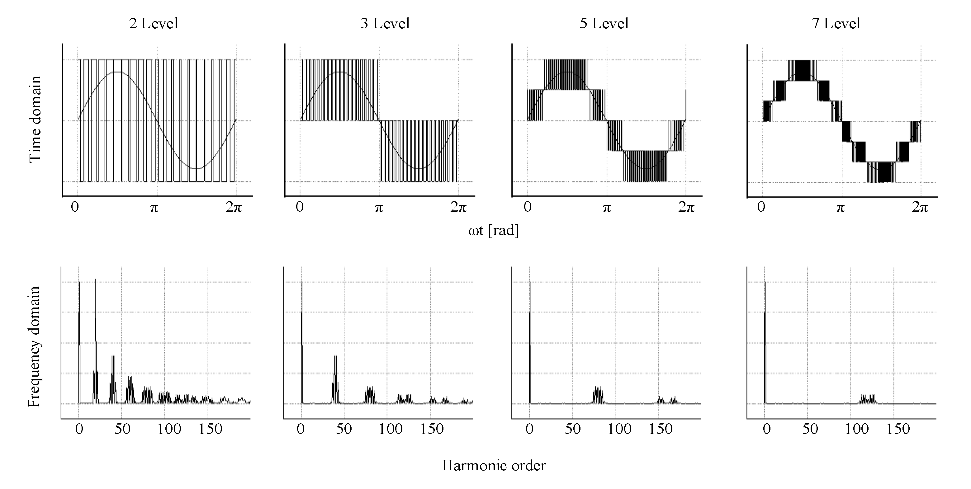
- Lower harmonic content and more concentrated in the fundamental component and at high frequencies. As illustrated in Figure 1: (i) the greater the number of levels, the more closely the output waveform resembles a sinusoid; (ii) the higher-frequency harmonic content allows for easier filtering;
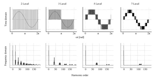 Figure 1. Influence of the voltage levels that an MLC can produce on the harmonic spectrum.
 - Possibility of integrating less bulky passive filters, thus minimizing implementation costs and system losses, mainly copper and core losses in ferromagnetic elements;
- Possibility of reducing the voltage stress (dv/dt) of the power semiconductors. This feature enables the integration of more standard semiconductors with the higher commercially available stock and lower costs. Additionally, it allows for mitigating electromagnetic interference problems caused by high dv/dt values when switching semiconductors. Nevertheless, by reducing the dv/dt stress, it is also possible to reduce the galvanic isolation stress;
- Possibility of reducing switching frequencies, minimizing switching losses and semiconductor voltage stress;
- Simpler and faster maintenance service: just exchange the damaged submodule with a functional one;
- Enable the easy integration of renewable energy sources and energy storage systems.
All these features are very attractive, especially for high-voltage power distribution applications. An example of the integration of an MLC in high-voltage direct current (HVDC) systems can be seen in [5,6,7,8,9]. A distributed control of MLCs for HVDC application is proposed in [10], and fault conditions analyses can be found in [11,12,13]. Another major focus of MLC applications lies in solar photovoltaic [14,15,16,17,18,19,20,21,22] or wind farms onshore [23] and offshore [24,25,26,27]. The MLC can also interface with energy storage system (ESS) [28,29,30,31,32,33,34,35]. Regarding electric mobility, the MLC has great applicability in feeding railway electric systems [36] or operating as active power conditioner [37,38] to mitigate power quality problems in the railway system. Additionally, the MLC concept can be employed in electric vehicles for traction purposes [39,40] or to interface with an onboard ESS [41,42]. The MLC has also been implemented in marine propulsion [43,44]. The mentioned characteristics potentiated the integration of MLCs for active conditioners in order to mitigate power quality problems, acting as a static compensator [45,46,47,48,49,50] or distribution STATCOM (DSTATCOM) [51]. Emerging power electronics concepts, such as solid-state transformers, have also been exploring the potential of the MLC [52,53,54,55,56].
In [1] a comparative analysis, five submodule topologies capable of integrating an MLC solution are described, presenting conclusions regarding the allowed operating modes, number of semiconductors, and DC bus constitution. In [57], the authors present an analysis of different MLC topologies, highlighting the submodules: neutral-point-clamped (NPC), flying capacitor multilevel converter (FCMC), and cascaded full-bridge (CHB). Applicability of these topologies, as well as electrical magnitudes of some existing state-of-the-art prototypes developed, are presented.
Akagi in [58] explains the evolution of the modular multilevel converter (MMC) and modular multilevel cascaded converter (MMCC) concepts. The terminology adopted by Akagi was MMCC to portray modularity and the multilevel cascaded power electronics converters. Thus, the presented study depicts the analysis, classification, terminology and applications of different MMCC configurations, each cell being composed of a full- or half-bridge. Experimental results for a low-scale MMCC for an energy storage site and driver engine are presented, highlighting the good immunity of the system to electromagnetic interference.
The authors of [59] present the evolution of the topologies of the submodules that constitute an MMCC, highlighting the mathematical model of the system. Technical challenges and future trends are also presented. In [60] the authors pretended hybrid modular and multilevel solutions based on the combination of submodules of different topologies. An analysis of the evolution of the different cells is also presented. The authors of [61,62] present a study of the evolution of power electronics solutions for railway applications, highlighting the solutions implemented by different manufacturers where the submodules of the modular and multilevel systems are based on solid-state transformers. The evolution of the solutions shows a tendency for the submodules to share the same DC bus, with the output of each submodule being cascaded to the adjacent submodule. Prototypes of the power electronics converters and transformers used in different solutions are also presented and analyzed. Further studies can be found in [62,63,64], where different topologies, configurations, controls, and end applications for MMC are analyzed.
The main focus of the authors’ contribution in [65] lies essentially in the comparative study of different PWM techniques for the conventional MMC topology. In turn, a review of control techniques, as well as the working principle of an MMC, highlighting existing state-of-the-art techniques and future contributions, is presented in [66]. Applications of the MMC are also listed.
From the state-of-the-art review articles, some research gaps were found that this article aims to fill. From the study conducted, it was found that the review articles focus primarily on the conventional MMC topology, with each submodule consisting of either a half-bridge or full-bridge. There are other review studies but with other topologies, as well as review studies for cascaded solutions. The review of the applications is always limited to the studied topology. In turn, as far as the control algorithms are concerned, no complete study was found that implements all the modulation techniques in order to quantify the best solution. Thus, there exists a lack of analysis of the power imbalances between submodules, the harmonic distortion rate, and the harmonic content generated as a function of each PWM technique.
This paper aims to provide a critical, thorough and objective analysis of different power electronics converter topologies that can be integrated into modular and multilevel systems. Additionally, it is intended to contribute a comparative study of different modulation techniques to be implemented in MLC systems. It is expected that this study can serve as an implementation manual for different researchers, students, and engineers that have been developing work in this area, thus contributing a starting point for the development of new solutions. This paper is structured as follows: in Section 1, an introduction to the MLC concept is given, presenting the main advantages as well as applications of the MLC; in Section 2, an analysis of the MLC concept is performed, reviewing some power converters topologies that can be integrated into the MLC; Section 3 is dedicated to presenting PWM techniques to control MLCs; Section 4 presents a comparative analysis of the different PWM techniques in cascaded four full-bridge submodules; Section 5 presents the main conclusions of the review study.
2. Multilevel Converter
The DC–AC power converters, also known in the literature as inverters, are usually classified according to the constitution of the DC bus: voltage source inverter (VSI) or current source inverter (CSI). In general, the DC–AC power converters have as their main objective the synthetization of an AC component from a DC source, using fully controlled semiconductors. The AC output amplitude and frequency are adjusted from the implemented control algorithms. Regarding the power semiconductors, some examples of technologies can be (i) insulated-gate bipolar transistor—IGBT, (ii) metal-oxide-semiconductor field-effect transistor—MOSFET, (iii) insulated gate collector transistor—IGCT, etc. For the following analyses presented in this topic, the IGBT will be used as a power semiconductor due to its predominance in the implementation of these types of high-voltage and high-power applications.
In general, the DC–AC power converters have discrete values in their output, requiring precautions in their implementation in order to safeguard system integrity. That is, considering that the control of IGBTs is based on PWM techniques, the output waveform of the DC–AC power converter will have a resulting frequency equal to or multiple times the switching frequency of each IGBT. Although the output waveform is not sinusoidal, as desired, the frequency of the fundamental component is close to the desired one, as can be seen in Figure 1. This characteristic presents some requirements to be met, depending on the application.
VSIs have high discrete dv/dt output values. In order to smooth the waveform, the load needs to be inductive. Otherwise, with capacitive loads, current spikes would appear. This concludes the need to include an inductive filter between the output of the VSI and the load. In turn, CSIs have high discrete di/dt output values. Therefore, in order to smooth the output waveform, the CSI load should be capacitive. Otherwise, with inductive loads, voltage spikes would appear, thus concluding the need to include a capacitive filter between the output of the CSI and the load.
In order to integrate power electronics converters in high-voltage applications (for example, a VSI), it is necessary to increase the amplitude of the DC bus voltage. From a practical point of view, the DC bus voltage should be higher than the peak value of the power grid voltage. As a consequence of increasing the DC bus voltage, larger inductive filters will be required in order to mitigate the increase in dv/dt variations.
Considering the implementation of these types of solutions, it is also necessary to take into consideration the semiconductors available in the market. Aspects such as blocking voltages, switching frequencies, and stock quantities are important in industrial applications. However, semiconductors with high voltages and switching frequencies have limited stock, being more suited to specific applications of limited requirements, and are not very attractive either in research and development or in industry. In turn, semiconductors with medium voltages and switching frequencies present themselves as a mature and predominant technology in the market.
Figure 2 illustrates the evolution and emergence of new MLC topologies. The MLC concept emerged in the 1970s, invented and patented by William MacMurray, with the cascaded full-bridge configuration. The same inventor pioneered another approach, where the full-bridges were in parallel, sharing the same DC bus, with low-frequency cascaded transformers at the output of each submodule of the full-bridge [67,68]. The cascaded full-bridge topology has been matured, widely used by ABB (Oerlikon, Switzerland), featuring a modular and robust structure that is fault tolerant with the addition of bypass switches. The main disadvantages reside in the need for each submodule to require a DC-source. The cascaded transformer approach mitigates this problem, obtaining a single DC-source on the lower voltage DC-side. Although it allows a simpler DC bus balancing control algorithm, it requires special care in the sizing and control of the AC side in order to avoid the saturation of the transformers. In order to avoid an average value of the magnetic flux variation, it is recommended that the system start at 90° or to 270°, taking into account an application of AC. Thus, the flux density integral from the instant of 90° to 270° has a similar symmetrical value to the integral from 270° to 90°, obtaining a null value at each period [69]. Otherwise, the flux density would have an average value, which could saturate the ferromagnetic core. This is especially important for ferromagnetic cores that are not laminated and have low flux density values.

Figure 2.
Evolution and emergence of new MLC topologies.
In 1980, the NPC topology was presented and patented by Baker [70]. NPC topology attracted researchers, becoming best known when, in 1981, Akira Nabae and Hirofumi Akagi presented and experimentally proved its mode of operation [71].
A “multilevel high-voltage chopper” in the literature best known as FCMC topology, was introduced by Meynard and Foch in 1992 [72].
The modular multilevel converter (MMC) topology, emerging in the new millennium, is a major driver in power electronics for high-voltage and high-power applications. This concept can be implemented with submodules based on topologies such as half-bridge [73], full-bridge [73], NPC [74], T-type NPC (TNPC) [74], or FCMC [75]. Despite all the previously mentioned advantages concerning the MLC concept, MMC presents some added challenges, such as [8]
- The sizing of the inductive and capacitive elements: The inductor must be sized in order to decouple the DC component from the AC, as well as to minimize the short-circuiting of the DC bus;
- The pre-charging process of the capacitors: Whenever the MMC is initialized, the capacitors are discharged, requiring a pre-charging mechanism in order to minimize the inrush current;
- DC bus regulation: The DC bus must be constantly regulated to a reference voltage in order to allow the correct operation of the MMC, thus requiring several sensors and signal-conditioning circuits. The imbalance of DC bus voltages between the different submodules causes the emergence of circulating currents, requiring algorithms and mechanisms in order to mitigate this problem;
- The ripple in the DC bus: The harmonic spectrum of the DC bus voltage of each submodule will be concentrated in the fundamental frequency and in the second-order harmonic. Knowing that the voltage ripple is inversely proportional to the frequency of the fundamental component, this effect is more severe in variable speed applications, namely at start-up and at low motor rotating speeds. As such, capacitors with higher capacity are required, inflating implementation costs;
- Circulating currents: This effect does not affect the AC component of the output voltage and current. However, it increases the root mean square (RMS) and peak value of the arm current, consequently increasing the converter losses and the DC bus ripple;
- Fault-tolerance: The MMC is usually implemented with redundant submodules, ready to enter into operation in case of faults. One of the challenges is the decoupling of a damaged submodule and consequent coupling of an operational one, in a dynamic way, without the emergence of inrush currents. Another challenge is the development of protection mechanisms, namely circuit breakers, capable of shutting down the system in the event of a failure, which is especially important in HVDC applications.
In general, it was possible to notice that the development of modular and multilevel power electronics solutions presents an added challenge, mainly in high-voltage and high-power systems. The development of these systems requires a fully coordinated team: highlighting teams of engineers dedicated to the digital control system and implementation of algorithms in microcontrollers; teams dedicated to the development of simulation models; teams dedicated to the development of power electronics converters, semiconductors, transformers, and other magnetic components; a team dedicated to electromagnetic compatibility and signal isolation; mechanical teams for the development of the modular structure and heatsinking; and Computer-Aided Design (CAD) engineers for both the mechanical and electrical systems, such as printed circuit boards (PCB), among others. The development of this system is multidisciplinary, with complex development and validation tasks.
One of the future trends concerning the MLC concept is the cascading of different power converter topologies capable of synthesizing five or more output voltage levels [3]. Different configurations for the MMC using a solid state transformer (SST) can be seen in [61,63,76,77].
System modularity and expandability presented new challenges, particularly in control systems. Knowing that microcontrollers have a limited number of input and output peripherals, the expandability of the system also became limited. One solution would be to integrate a Field Programmable Gate Array (FPGA), since it has a large number of configurable input and output peripherals. However, the system would have to be oversized, or it would lose modularity [76]. In order to mitigate this disadvantage, decentralizing the control has been proposed [78,79,80,81,82]. As a future trend, each submodule would have its own microcontroller, the slaves, and there would be a communication channel with a central unit, the master. This way, the master would be responsible for managing and configuring the different submodules, distributing the tasks to each of them. Therefore, and for correct operation, the communication must be fast, not susceptible to interference, synchronized, and robust in case of failures. Possible contributions include the development of algorithms for plot management, configuration, and control of each submodule. The hardware is equally important, requiring a balanced solution between parallel communication (fast but with a larger number of connections) and serial communication (longer time but fewer connections).
As the system expands, more voltage sensors, more current sensors, more communication, and more monitoring peripherals are needed. As such, and in order to make a simpler, more compact, and cheaper solution, the development of sensorless control algorithms becomes important and interesting [83].
In analyzing the submodules, the assiduous presence of capacitors in the DC bus becomes evident. It becomes important to minimize bulky and lifetime-limited capacitors by using balancing algorithms or appropriate modulation techniques in order to extend the lifetime of the components [83].
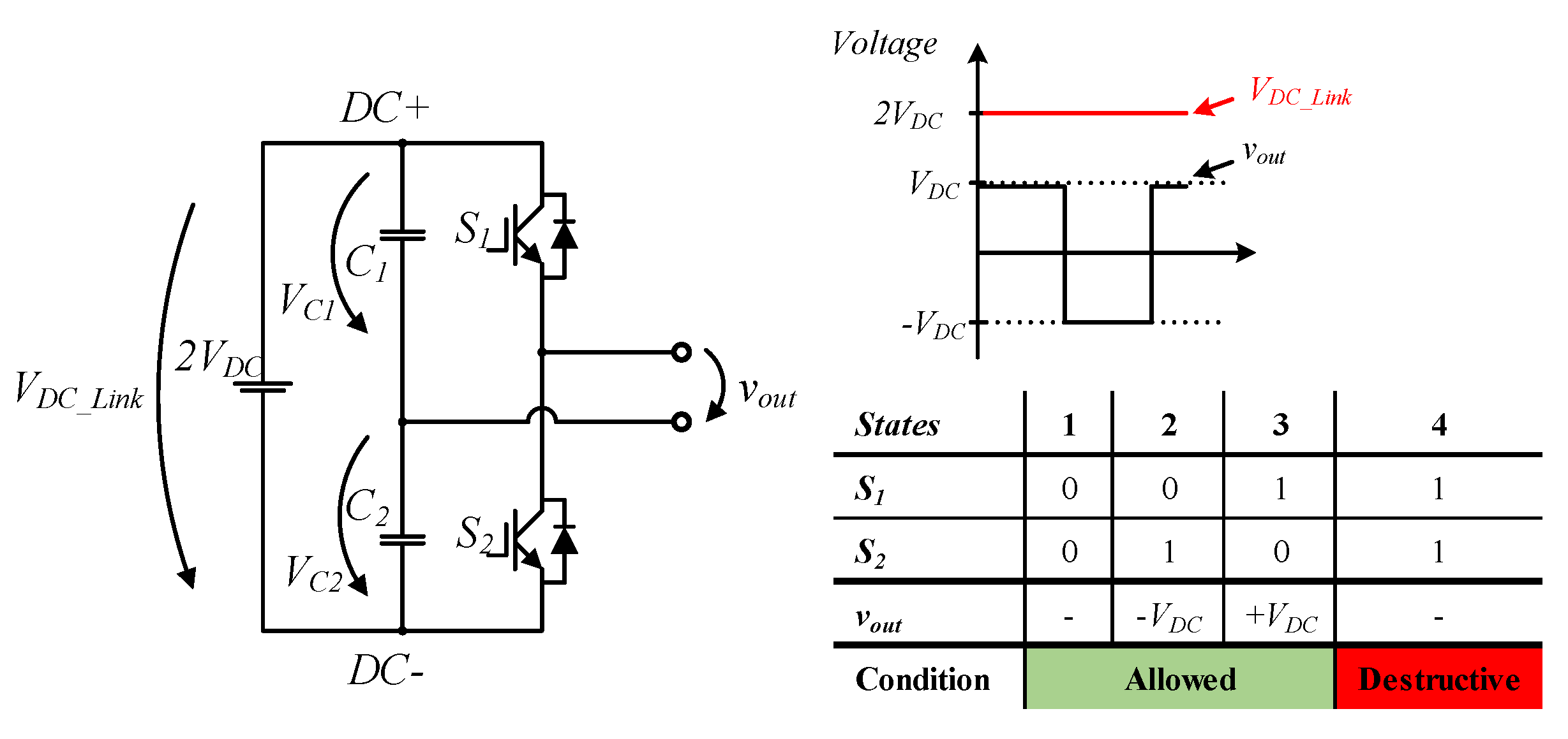
In the following subtopics, different topologies of MLC are analyzed. The solution is presented, highlighting the operating modes, as well as presenting some examples of developed practical systems and prototypes. The multilevel system can be achieved either by expanding the topology or by modularity, where more submodules of the same topologies are inserted in series. To highlight that, considering the DC bus, it is necessary to create a dead time for switching between states. The dimensioning of this dead time is crucial in order to avoid a short circuit of the voltage source in the VDC_Link, as well as to avoid potentially destructive operating states.
2.1. Half-Bridge Submodule
The half-bridge topology has great versatility, with two different approaches: one with the DC bus split and one with a single capacitor on the DC bus.
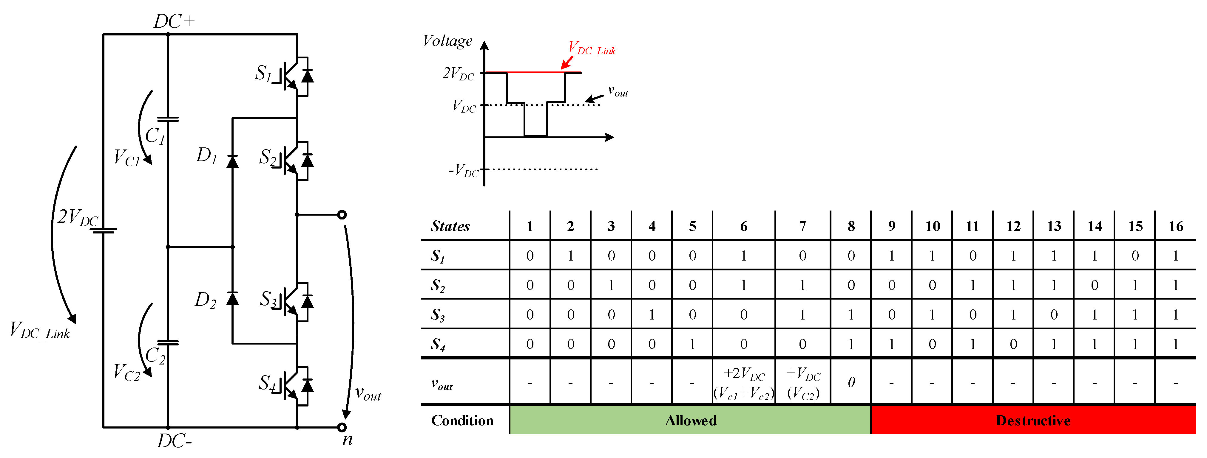
Regarding the split DC bus half-bridge topology, it has a simple structure, as shown in Figure 3. This topology features two capacitors on the DC bus and two IGBT devices connected in series. The midpoint of the capacitors is used as the reference potential for the output voltage, vout, of the converter [73]. As a consequence, to be able to generate an output voltage with a value of VDC_Link, the DC bus will need to have twice the voltage. Thus, each capacitor that makes up the DC bus will have a voltage equal to VDC_Link. Figure 3 shows the allowed states of operation of the topology.
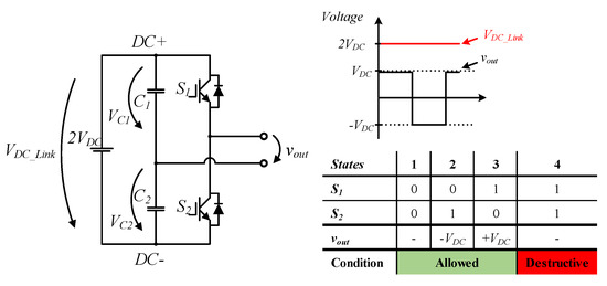
Figure 3.
Half-bridge with split DC bus topology and operation principle.
In analyzing the literature, it was possible to verify that this topology is not used as a submodule in solutions such as MMC. However, it was possible to verify the integration of this topology together with other power electronics, presenting a hybrid multilevel solution. A five-level hybrid solution is presented in [84], where two half-bridge submodules are cascaded with a full-bridge. Another three-phase hybrid solution is presented in [85], where, for each phase of the electrical system, there are three cascaded half-bridge submodules, two with common DC bus, and one with split DC bus. Although not popular in multilevel applications as single submodule topology, this topology is widely used as an integral part of one of the stages of an SST [86,87,88].
In turn, as far as the half-bridge topology with single DC bus is concerned, it features a single capacitor on the DC bus and two IGBT devices. As a consequence, it only allows two levels of output operation, as represented in Figure 4, always operating with a DC component [73]. This topology is commonly referred to as “chopper cells” [89]. In order to interface with AC applications, this topology needs an auxiliary submodule in order to create a symmetrical state. Thus, it is possible to identify two arms: an upper one responsible for synthesizing the positive semi-cycle and a lower one responsible for synthesizing the negative semi-cycle. The more levels of operation, the more submodules needed. Note that each submodule only allows operation in two quadrants: positive voltage and bidirectional current. However, its simplicity in terms of hardware is quite attractive for the constitution of MMC solutions.
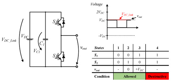
Figure 4.
Half-bridge with single DC bus topology and operation principle.
A hybrid solution is presented in [42], in which they use different cascaded half-bridge submodules. The output is connected to a full-bridge power converter responsible for unipolar modulation. This system is replicated for each phase of the electrical system. Another hybrid solution, for the MMC concept, is presented in [7], where they use a combination of half-bridges with full-bridges. in analyzing the state of the art, it is in the MMC concept that this half-bridge submodule is widely used [38,45,90].
An example of an MMC using 48 half-bridge cells with a 3 kV DC bus and 550 kW output power can be found in [91]. Among several functionalities, the system’s decentralization with redundant operating mechanisms should be highlighted. Considering the complexity of the system, it is important to highlight that this prototype was developed by 26 researchers. The mathematical model of an MMC, as well as some diagram control algorithms, can be found in [77].
2.2. Full-Bridge Submodule
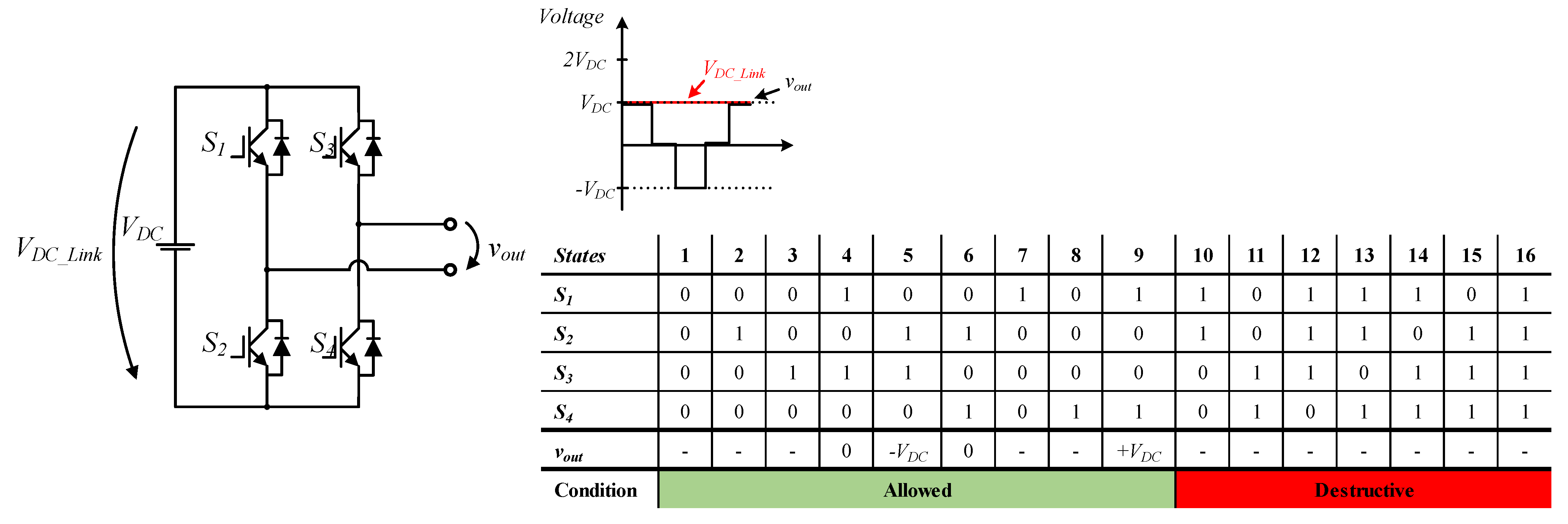
The full-bridge topology consists of four IGBT devices and a DC bus. This power converter topology features two IGBT arms, with each arm consisting of two more IGBTs. The output terminals of the power converter are connected to the midpoint of each arm. This configuration characterizes the converter commonly known as the “H-bridge” [73].
Regarding the operating modes, it should be noted that if the DC bus is a voltage source, the IGBTs that make up each arm should be driven complementarily in order to avoid a short circuit to the DC bus. For this purpose, creating a dead-time for the IGBT devices of the same arm is recommended. In turn, if the DC bus is constituted by a current source, a path for the current must always be maintained. As such, it is necessary to create an overlap time of the semiconductors of the same arm [92]. The operating modes considering a DC voltage source on the DC bus are shown in the Figure 5.
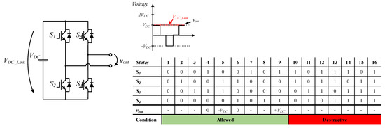
Figure 5.
Full-bridge topology and operation principle.
As far as control is concerned, with the unipolar modulation technique, it is possible to obtain a resulting output frequency of twice the value of the IGBT switching frequency. This is due to the configuration of two arms in parallel. This characteristic enables the integration of less bulky and cheaper passive filters. Nevertheless, this topology allows for operation in four quadrants, as well as generating bipolar signals. However, in case of failure of an IGBT, the submodule is totally inoperable [1].
Regarding the practical implementation, it is possible to identify the existence of different semiconductors referenced to the same potential, which enhances the implementation of simpler and cheaper driver circuits. Nevertheless, this topology is able to generate an output signal with amplitude equal to that of the DC bus. However, during the operating states, there will always be two semiconductors in conduction, presenting an output voltage slightly lower than the DC bus voltage due to the value of the direct voltage of the IGBT.
One of the most common approaches used in multilevel systems with the full-bridge is to cascade different submodules [27,93]. The larger the number of submodules, the higher the output voltage levels and hence the synthesis of a closer to sinusoidal output waveform. Using different voltage levels at each DC bus allows the creation of more voltage levels, consequently decreasing redundant states of operation [39]. In [4], the valid switch states and redundant stages for a five-level cascaded full-bridge are presented. The implementation of the space vector modulation technique (SVM) is the most recommended since it allows the logical combination of each IGBT to be determined in order to generate the desired state. However, the DC buses of each submodule are floating, requiring isolated sources for each, inflating the cost and complexity of implementation [27]. Solutions to mitigate this disadvantage have been developed, such as the use of a single DC-source in one of the submodules, using the redundant states to load the DC buses of each submodule in cascade [94]. SST emerges as an interesting concept that, in addition to allowing the creation of isolated sources for each DC bus, also allows for bidirectional power [61,95].
Another approach consists of connecting different full-bridges in parallel, adding an isolating transformer at the output of each full-bridge. Each submodule shares the same DC bus, with multiple IGBT devices referenced to the same potential, and the secondary side of each transformer is connected in series with the transformer of the adjacent submodule [96,97]. Combining the different transformer ratios of each transformer again allows for a greater number of generated voltage levels by foregoing redundant states [98,99]. In [77], the switching pattern obtained considering an MMCC composed by four full-bridge submodules with four transformers with different turns ratios is presented. However, it should be mentioned that this approach causes an imbalance in the operating powers of each submodule. According to [16], the submodule with a lower switching frequency contributes 80% of the total power transferred. The lower the switching frequency of each submodule, the higher the power. Regarding the power transformers, special attention needs to be paid to their sizing, as well as the instant to start the control.
These approaches have enhanced the study and implementation of innovative solutions, such as solid-state transformers. In [52], it is possible to verify an example of SST application. Each submodule is composed of a dual active bridge (DAB), following a full-bridge. The primary side of each submodule is connected to a single low voltage DC bus, and the outputs of each submodule are connected in series with the adjacent submodule. Among other features, the following advantages can be highlighted: connection of different submodules to a single DC bus, which allows simplification of the control of the DC bus; integration of the phase-shift technique for power transfer in the high-frequency isolating transformer, minimizing the probability of saturating the ferromagnetic core since the flux density cancels out every two switching cycles; a higher power density in the transformer.
2.3. Neutral Point Clamped Submodule
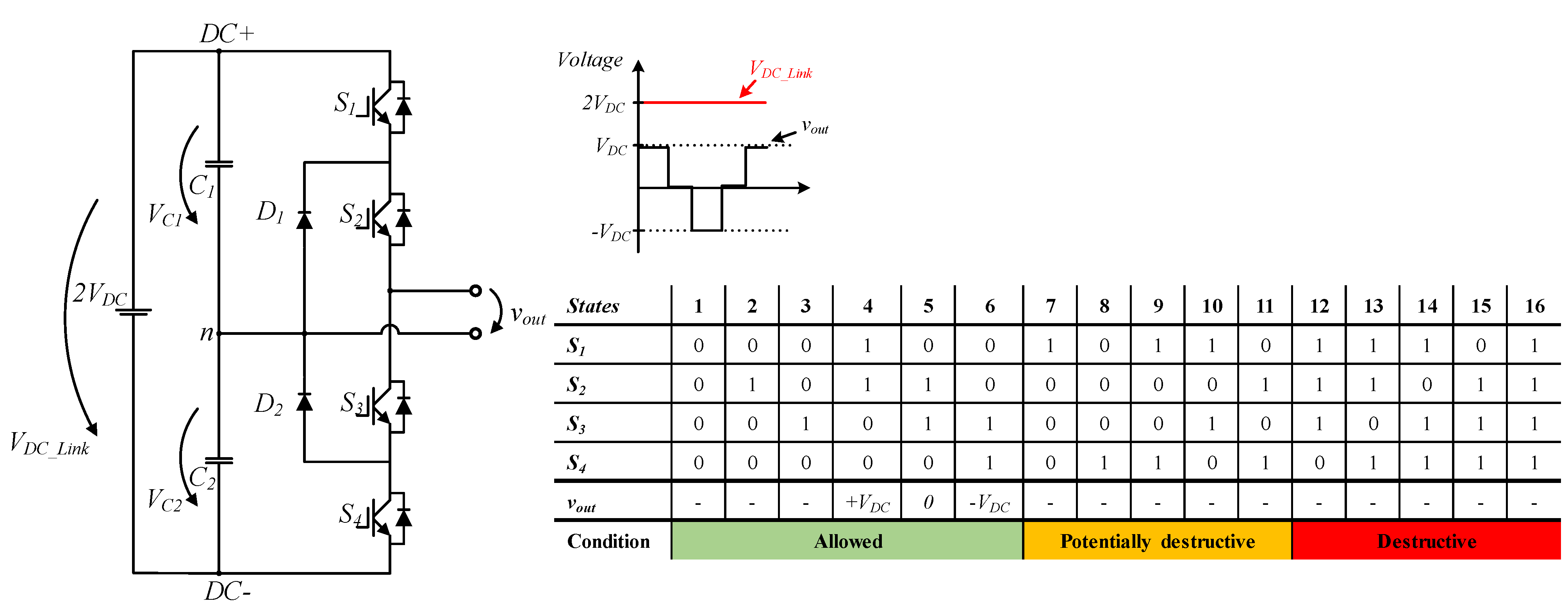
The NPC power converter consists of two arms, as illustrated in the Figure 6. One of the arms, for energy storage and decoupling purposes, consists of two capacitors connected in series, with the midpoint used as the reference potential. In turn, the other arm consists of four IGBT devices connected in series, with the midpoint used as the output terminal [74].
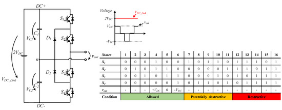
Figure 6.
Conventional NPC topology and operation principle.
The IGBT devices located in the upper part of the arm (S1 and S2) must be activated in a complementary way to the IGBT devices located in the lower part (S3 and S4). In this way, a short circuit to the DC bus is avoided. Depending on the modulation technique implemented, bipolar or unipolar, this topology presents the versatility to generate two or three output voltage levels [4,89].
This topology is expandable, requiring the addition of more semiconductors and capacitors. In [74,100], it is possible to find other variations of this topology, namely in its expandability to more levels. Control algorithms and applications are also presented. However, the more levels, the more diverse the current paths of the converter, with short and long paths to charge the DC bus. Due to this difference in impedances, even with similar semiconductors, this topology has as a major disadvantage the imbalance of the DC bus voltages. Nevertheless, the modulation technique adopted can intensify voltage imbalances. In order to mitigate this problem, different solutions have been explored: active control, active auxiliary circuits, and passive auxiliary circuits. A solution based on active control presents a greater complexity of implementation, requiring a microcontroller with greater processing capacity. In turn, active auxiliary circuits require additional hardware, essentially increasing complexity and cost. Finally, passive auxiliary circuits are characterized by increased system losses, decreasing the efficiency of the converter. This topology only has redundant states of operation between phases (phase–phase) of the power grid and not in the same phase power line. As such, if redundancy is an imposed feature, this NPC is only viable in three-phase applications, where, for example, a six-level NPC can obtain 216 redundant states [101]. The lower the modulation index, the higher the redundant states are [4]. Another variant of the NPC topology used as a submodule can be found in the Figure 7.
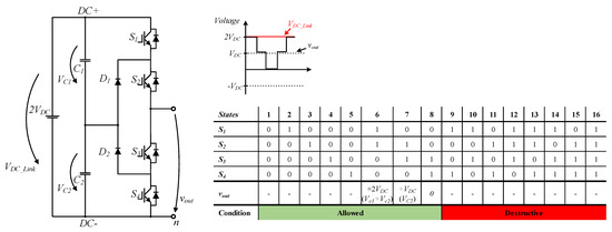
Figure 7.
Submodule NPC topology for cascaded applications and operation principle.
A cascaded MLC based on NPC cells was presented by M. Carpanet et al. in [102]. A novel hybrid MLC based on NPC cells cascaded with half-bridge chopper cells for three phase applications was presented in [103]. An SST solution composed by a multilevel DAB converter was proposed in [104], where a three-level NPC was adopted to be used on the high-voltage side.
2.4. T-Type Neutral Point Clamping Submodule
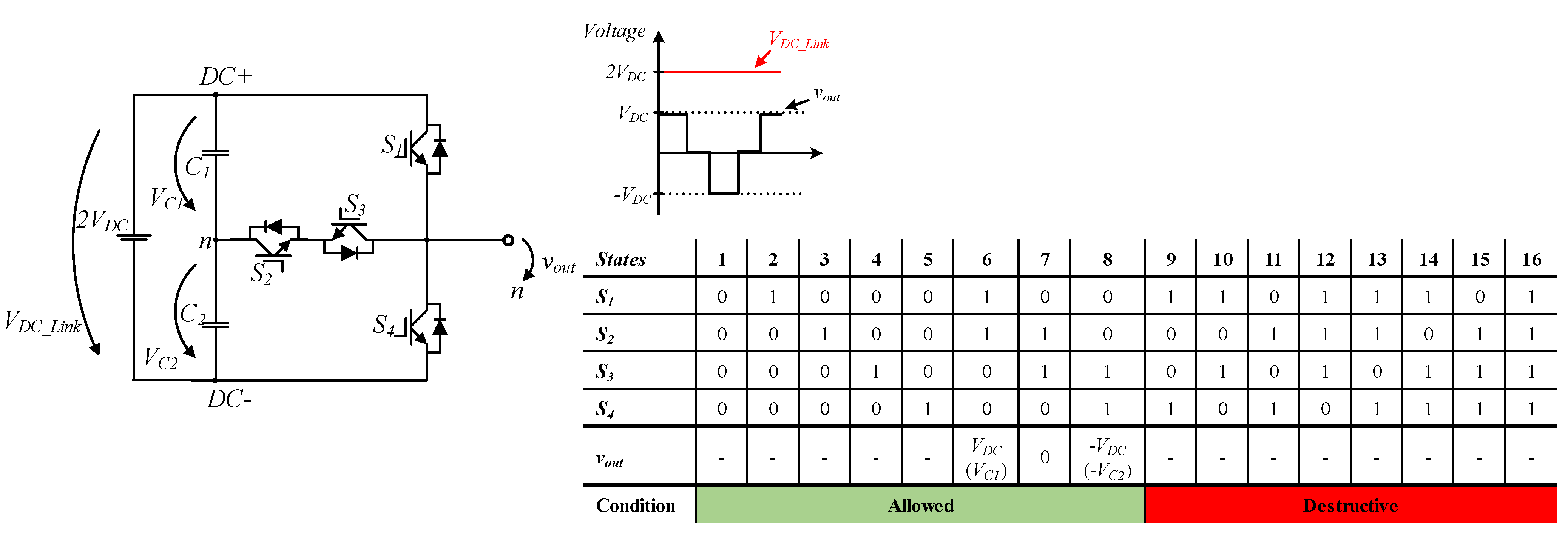
The T-type NPC (TNPC) topology has a structure similar to the half-bridge topology with a split DC bus, with the addition of a bidirectional switch between the midpoints of the DC bus and the IGBT arm, as illustrated in Figure 8. The bidirectional switch consists of two IGBT devices connected in anti-series. This configuration is also referred to in the literature as a neutral point pilot (NPP) [59,89].
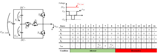
Figure 8.
T-NPC topology and operation principle.
The design of three-level T-NPC for high speed motor drives using 150 kVA silicon-carbide (SiC) MOSFET was presented in [105]. An MMC solution based on a new four-level T-NPC topology cell was presented in [106].
2.5. Flying Capacitor Multilevel Converter Submodule
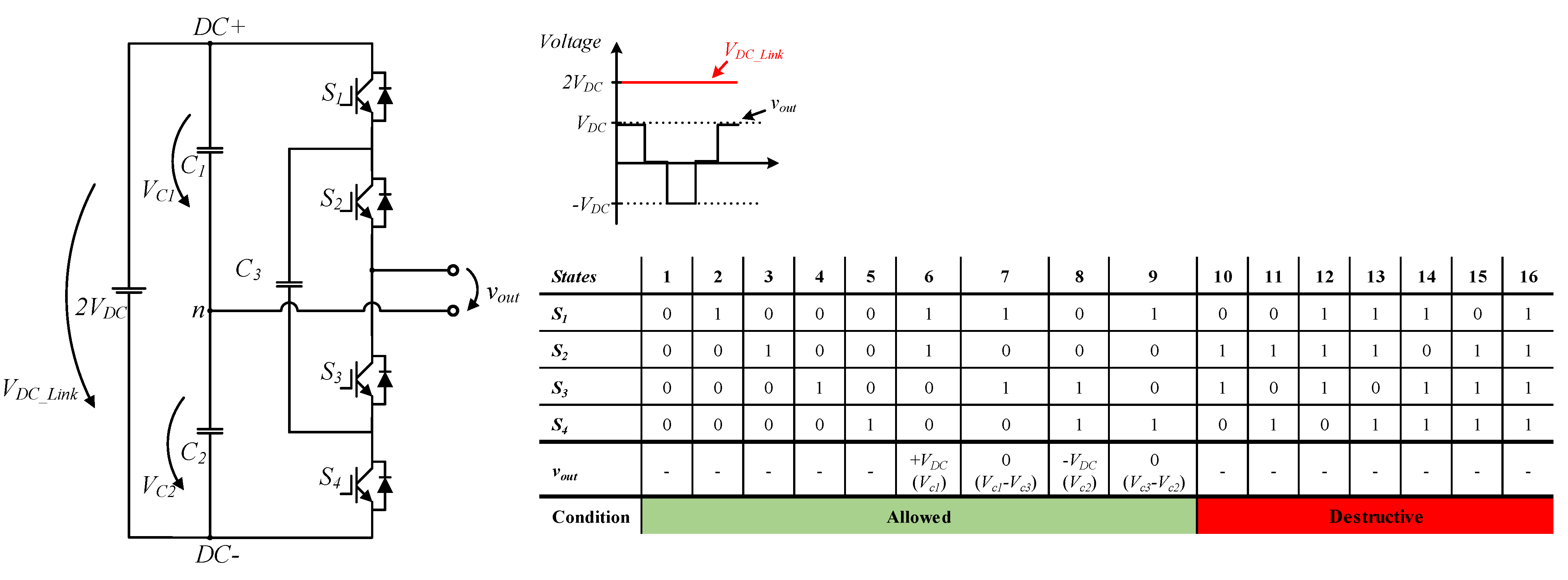
The FCMC topology has a similar structure to the NPC, with the diodes being replaced by a capacitor, as shown in Figure 9. Consequently, the center-located IGBT devices cannot be driven simultaneously in order to avoid short-circuiting the flying capacitor, C3. In order to ensure proper operation of the topology, the voltage of the floating capacitor must be similar to the voltage of each capacitor in the DC bus [100]. Regarding the power semiconductors, these must have a blocking voltage higher than the voltage of each set of capacitors of the DC bus [72].
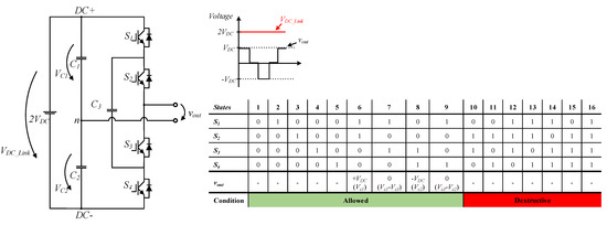
Figure 9.
FCMC topology and operation principle.
In analyzing the schematic of the topology presented in Figure 9, it is possible to see the predominance of capacitive elements. As such, the topology is susceptible to inrush currents at the startup instant [74]. The implementation of auxiliary pre-charge circuits is recommended in order to minimize this disadvantage. A simple solution is to include resistors between the DC-source and the capacitors during the pre-charge process. As soon as the voltage in the capacitors reaches a minimum operating value, a switch is activated to bypass the resistors. This way, the converter can operate in steady-state without the losses associated with the resistors. In [100], it is possible to find other variations of this topology, namely in its expandability to more levels. Control algorithms and applications are also presented.
The capacitors are the main energy storing element in this topology, playing an important role for the correct operation of the system. The system performance is directly related to the voltage ripple in the capacitors that, consequently, will influence the energy stored in the capacitors. By increasing the switching frequency, it will be possible to decrease the capacity of the capacitors. However, electromagnetic compatibility problems will be intensified. Nevertheless, special care must be taken when choosing the technology of the capacitors, with electrolytic capacitors having a higher capacity despite a poor frequency response when compared to other technologies, such as film capacitors. What is also important is the lifetime of the capacitors, which is low, as well as the space occupied. Comparing the floating capacitor topology with the NPC, it can be concluded that the diodes have a smaller volume than the capacitors.
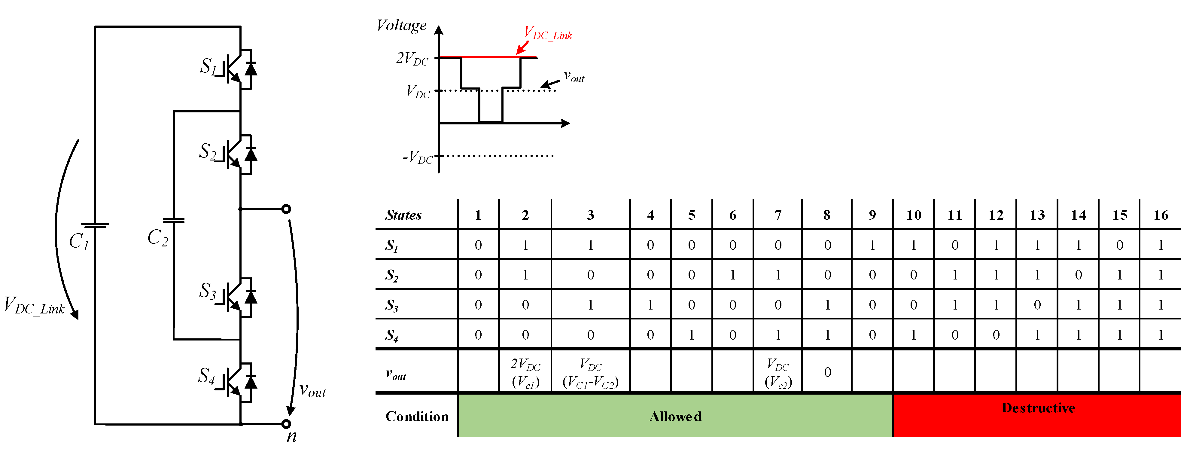
The Figure 10 shows the electrical scheme of the FCMC topology as a submodule presented by Meynard and Foch in 1992 [72]. It should be mentioned that semiconductors S3 and S4 must be activated in a complementary way with semiconductors S1 and S2, respectively. Some potentially destructive operating states could be reached if the control signals are not correctly configured, namely in the state where only S1 is active. From an operating point of view, the DC bus has twice the voltage of capacitor C2. As such, there is a redundant state in which voltage VC2 can be created with S1 = S3 at off and S1 = S2 at on (vout = VC2) or else S1 = S3 at on and S2 = S4 at off (vout = VC1 − VC2) [8]. The redundancy of states, with the expandability of the system, presents itself as an advantage in order to allow different states to charge or discharge a given capacitor [107]. An explanation of the operation modes of this submodule topology can be found in [8,100]. In [4] is presented the switch stage for a six-level FCMC, where it is useful to select a specific capacitor to charge or discharge during the switching pattern. By increasing the number of levels of the FCMC, more redundant states are obtained for different levels [4].

Figure 10.
Conventional submodule NPC topology for cascaded applications and operation principle.
The concept of floating capacitors was used in a project presented for the Google/IEEE Little Box Challenge in [108]. The authors developed an ultra-compact seven-level 2 kW FCMC, with a 450 V DC bus for 240 VAC networks, with a power density of 13.2 W/cm3 and an efficiency of 97.4%. Cascaded FCMC submodules are used to create a seven-level stair waveform, followed by a full-bridge converter so that it is possible to generate a sinusoidal output waveform with a mean value of zero.
2.6. Submodule Topologies Comparison
As analyzed so far, the different topologies have different functionalities, characteristics, and requirements for their correct operation. In this topic, a comparative analysis of the different topologies is performed, some of the characteristics being patent in Table 1. It should be noted that the comparative analysis is carried out from the implementation point of view. That is, the variables are adjusted in order to meet a requirement, such as in the case of the DC bus: the voltage was adjusted so that the power converter could generate an output voltage of VDC.

Table 1.
Comparative table of submodule topologies.
In analyzing Table 1, it is possible to conclude that the greater the number of IGBT devices making up the topology, the greater the number of output voltage levels one can synthesize. An example of this is the half-bridge topology that, with two IGBT devices, can only generate two voltage levels. In contrast, the remaining topologies, with four IGBT devices, can synthesize three levels.
With respect to the DC bus, it can be concluded that topologies with a split DC bus, need the DC bus voltage to be twice the value of the desired output voltage. Nevertheless, splitting the DC bus needs additional sensors and signal conditioning circuits, inflating the cost and complexity of implementation. Nevertheless, regarding the half bridge submodule with a single DC bus, it should be noted that for AC applications an additional module is required. Thus, depending on the number of output voltage levels desired, module replication is required: with one arm responsible for the positive half-cycle and another arm responsible for the negative half-cycle. The duplication of components, namely in voltage sensors, signal conditioning circuits, and capacitors, requires more complex control algorithms, as well as a larger initial investment.
From a practical point of view, two characteristics of the full-bridge topology can be highlighted. The first is the existence of IGBT devices referenced to the same power. If the implementation approach involves associating different submodules in parallel with cascaded transformers, it would be possible to implement simple, robust, and cheaper driver circuits. On the other hand, the full-bridge topology is the only one that features arms with IGBT devices in parallel. This feature allows for obtaining the resulting output frequencies higher than the switching frequency. As such, it is possible to reduce the passive filters and consequently reduce weight, volume, costs, and losses in both the copper and core of the inductive components.
In Table 2, it is possible to identify different approaches for implementing modular and multilevel power electronics solutions for different end applications. The topologies of power electronics converters presented are the topologies that prevail in the final equipment, and there may be different configurations of connections.

Table 2.
Examples of MLC applications.
In turn, Table 3 shows a more detailed analysis from the point of view of implementation and functionalities of different MLCs on the market and developed prototypes. It is possible to compare different powers, input and output voltages, switching frequencies, and the number of levels of the implemented systems. The information presented is based on the information obtained in the study of each article.

Table 3.
Examples of MLC solutions and prototypes developed.
With this study, it is possible to verify that, regardless of the topology used for the MLC solution, the final application presents high power and voltage. However, the higher the system interface voltage level, the greater the number of submodules. However, there are medium-voltage, high-power applications that have a smaller number of output levels, e.g., applications, such as motor speed control, with IGCT as the power semiconductor of choice. It should be noted that in the solutions presented, despite some difficulty in finding this information in all the articles studied, the prevailing PWM technique is the PSC. Finally, it should be noted that the switching frequencies range from a few hundred Hz to a few kHz.
3. Fault Tolerance Applied on MLC and Gate-Driver Circuits
With the increase in the number of MLC operating levels and, consequently, the number of semiconductors and passive components, namely the capacitors, the probability of failure increases. According to [184], there are three zones that relate the probability of failure of an electronic component to its lifetime, whether measured in hours or number of cycles. The first zone is indicated as “infant mortality” or “debug period”, and its fault probability is high, as in the third zone, indicated as “wearout period”. The intermediate zone is characterized by the operation of the system after the debugging period, thus being classified as “constant failure rate” or “useful life period”. Knowing that the third zone indicates the end of the period of the entire system, and total replacement of the system is recommended, the first two are characterized by sporadic and unpredicted failures. Considering that the complexity and cost of an MLC increase with the number of levels, it is required that this system present robustness and fault tolerance. Thus, a continuous operation of the system is intended. In this way, in case of failure of any component or submodule, another operating state would be used in order to allow the continuity of system operation. This process requires four steps: fault detection, fault protection, fault clearing, and fault recovery [185].
In analyzing the bibliography, there is a constant study on the contribution of solutions and control techniques in order to increase the fault tolerance and viability of the MLC, including the use of redundant operating states, the use of redundant submodules, the use of auxiliary circuits and redundant material, and an upgrade on the control algorithms.
Redundancy mechanisms in case of failure are usually classified as “hot reserve” or “cold reserve” [186,187]. In the case of hot reserve, only one bypass is performed to the failure submodule, keeping the system in operation [188]. In turn, in the case of cold reserve, the failed submodule is replaced by a redundant submodule [189]. In this way, it is possible to predict that the hot reserve mechanism causes an asymmetric operation of the converter, as well as increasing energy losses. The increase in the rated operating conditions can lead to an increase in the operating temperature of the submodule, making it more susceptible to failures (25% of failures are caused by thermal fatigue [190]). In turn, the cold reserve mechanism presents as a major challenge the existence of mechanisms with galvanic isolation in order to preload the reserve submodules, in order to minimize transients and the impact on the performance of the control algorithms [191].
Regarding semiconductor failures, namely fully controlled ones, they can fail and remain in open or closed circuits (33% of failures are related to semiconductors [190]). In the event of a failure with the semiconductor in an open circuit (18% of failure cases [190]), it can either occur due to semiconductor burnout or loss of the control signal [190]. In this situation, the MLC may continue to function based on redundant states. There must be multiple redundant operating states for each operating level, or voltage levels will be lost. If it is not possible to obtain redundant states for all voltage levels, another mechanism is recommended. Different open circuit semiconductor failure detection techniques can be found, such as using the clustering algorithm or an algorithm based on a calculated capacitance [192]; using the MLC behavior observation method [193,194,195]; using the method based on the Sliding Mode Observer [196]; using the Luenberger Observer method [197]; using the Kalman filter [194]; or using the Fourier transform to detect a failure in an FCMC [198]. In turn, in case the failure causes a short circuit to the semiconductor (15% of failure cases [190]), a bypass mechanism is necessary in order to remove the failed submodule. This mechanism is also used in case of failure of passive elements. The inoperable submodule will remain in the system until the next scheduled maintenance. The bypass mechanism uses vacuum valves for quick disconnection of the submodule and is used in Siemens and Alstom MMC systems [5]. There are fault detection circuits with a quick response to over-voltages [199]. In [200], a method based on the behavior of the IGBT gate voltage is presented in which it detects the operation failure in less than 10 us, whether the failure is in a short circuit or open circuit. A voltage balancing strategy is presented in [201], which uses a voltage sensorless prediction method to locate the faulty submodule. Results obtained in “hardware in the loop” state that in 35.4 ms, the system can determine an open-circuit fault and in 3.2 ms a closed-circuit fault. After detecting the fault, the system isolates the faulty submodules and then recalculates the new system operating variables in order to suppress the missing submodule.
After the failure is detected, the system can continue operating with or without the addition of redundant submodules. In the case of redundant submodules, they can be connected to the system, using fast DC breaker mechanisms [202]. Another breaker circuit is presented in [203] for DC faults in MMC applications. The authors of [204] present a fault-tolerant solution based on spare submodules for topologies with cascaded full bridges in three-phase systems.
On the other hand, control techniques can be used in order to maintain the incorruptibility of the system without the need to add more submodules. One of the techniques is to keep the average bus voltage of each submodule constant (Method 1) or keep the average bus voltage of the entire system constant (Method 2) [5,205]. With Method 1, the remaining healthy submodules should be able to detect and compensate for the failure of the damaged submodule by adjusting the modulation index. With this technique, the operating voltages of each submodule are respected, although there may be overmodulation. More failures may occur as long as it is possible to obtain an output voltage of the MLC higher than the peak voltage of the electrical network, the modulation index being readjusted [5,205]. In turn, with Method 2, by keeping the average voltage of the entire system constant, it is necessary for each submodule to compensate for the failure by increasing the average voltages of the DC bus of each submodule. This method requires each submodule to be oversized in terms of operating voltages. That is, the nominal voltages of the capacitors and the blocking voltages of the semiconductors must be oversized, and this compensation may be limited with the increase in the number of faults [5,205]. A comparative study of these two methods is presented in [205]. A review of IGBT fault diagnosis methods and protection mechanisms for VSIs is presented in [206]. The determination of the energy stored in the capacitors for different methods of operation can be found in [5,191].
Considering that electrolytic capacitors have a limited lifetime, one of the malfunctions can occur on the DC bus. In this case, a quick response to mitigate the failure and provide a solution is necessary for the continued operation of the system. A DC bus short circuit fault determination method is presented in [207], obtaining a 1 ms response. Considering the propagation time of the signal over 200 km, the mechanism ensures that the protection is activated after 2 ms. Simple and inexpensive mechanisms for momentary DC bus failures have also been studied and proposed [12]. Auxiliary supplies to preload and minimize transients for a start-up is a costly but critical factor. Strategies using power loops in order to transfer power from neighboring submodules to the faulty cell are proposed in [208]; the system is based on an MMCC with hybrid energy storage systems (battery and supercapacitor).
Regarding the gate-drive circuits, the control of the semiconductor devices that make up the MLC solutions is presented as a crucial topic of analysis for the correct functioning of the entire system. The variation of the reference potentials can cause circulating currents, affecting the performance of the driver circuit. The increase in levels is reflected in the increased need for a highly reliable driver circuit. Nevertheless, as switching frequencies increase, semiconductor devices are subject to greater dv/dt stress, reaching values of 100 kV/µs in the case of the SiC MOSFET, imposing the requirement of low capacities between the input and the output of the driver [209]. Moreover, dv/dt stress can shorten the lifetime of electrical insulation, eventually breaking down and damaging the semiconductor. For the correct implementation of a circuit driver, three premises are necessary: (i) high electrical isolation, (ii) low coupling capacity, (iii) optimized driver circuit footprint layout [209]. However, it is impossible to provide a solution with the best of the three requirements; it is necessary to find a tradeoff solution, depending on the final application. Knowing the common mode current is directly proportional to the insulation capacity and to the dv/dt [209], the MLC solutions allow for assisting in the mitigation of the dv/dt. Other mechanisms can be implemented, some of which are presented below.
In [210], the authors analyze the effects of four different layout architectures for the gate driver circuits in order to minimize common-mode currents and, thus, minimize electromagnetic interference. A solution based on isolated sources with an optimized PCB layout to be integrated into a half-bridge submodule with overvoltage protection mechanisms was implemented in [38].
Taking into account that the use of isolated DC–DC sources for each driver circuit makes the solution more expensive, bulky, and energy inefficient; the authors of [211] present five driver methods applied in FCMCs based on bootstrap in order to mitigate these problems. Among the implemented methods, the following can be enumerated: (i) bootstrap at deadtime, more suitable for the gallium nitride (GaN) power switch; (ii) cascaded bootstrap with the low-dropout regulator, despite its simplicity, needs a high-voltage power supply; (iii) double charge pump, presents a low-efficiency solution; (iv) synchronous bootstrap, can reduce the voltage drop across the bootstrap diode but can be critical in applications with extreme duty cycles; (v) gate driver charge pump, features high efficiency. A smart gate driver is presented by [212], where bidirectional and fast communication channels are used, thus allowing a modular implementation and expansion of the driver system. A similar approach was implemented in an MMC in [213]. Another modular gate driver circuit used in an NPC is presented in [214] and analyzed in [215].
A driver circuit with short circuit protection at 5 µs, coupling capacitance of 1.2 pF, and tested for voltages up to 6 kV can be found in [209]. An analysis of different gate driver power supply techniques is presented in [216], mentioning wireless power transfer techniques for a single driver or multiple drivers, a conventional self-powering integrable cell, and a resonant and snubber capacitor. Solutions for the gate drive to mitigate the common modo noise [217] or resonant circuits [218] and equipped with optical fiber for the gate control signals can also be found. Other driver systems can be found in [219,220].
4. PWM Techniques Applied on MLC
In this section, different PWM modulation techniques applied in MLCs are presented and analyzed. These PWM techniques can be replicated with any MLC topology, requiring the correct configuration and sequence of PWM signals. It should be mentioned that there are PWM techniques that emerged in order to respond to some disadvantages of existing PWM techniques, not invalidating their implementation for other topologies for study and comparative analysis. Nevertheless, these techniques can be replicated for three-phase systems, where the correct configuration and phase delay adjustment of the carrier waveforms must be carried out for each phase of the three-phase power grid. A comparative study of the performance of different PWM techniques in the cascaded full-bridge topology is also presented.
4.1. Level-Shift PWM Technique
Level-shift PWM techniques were initially proposed for controlling MLCs with different IGBT devices in series, such as NPC or FCMCs. However, when these techniques were implemented in cascaded topologies, they created power imbalances between the different submodules. The unbalanced operation gives rise to the injection of harmonic content into the power grid and circulates currents between submodules [65]. In order to mitigate these problems, different approaches have been proposed, with some of them analyzed below.
The simplest modulation techniques concerning level shift can be listed as follows: phase disposition (PD), phase opposition disposition (POD), and alternate phase opposition disposition (APOD). These techniques have in common the vertical arrangement of different carrier waves. The carrier waves have the same amplitude and frequency, but their average value (offset) varies.
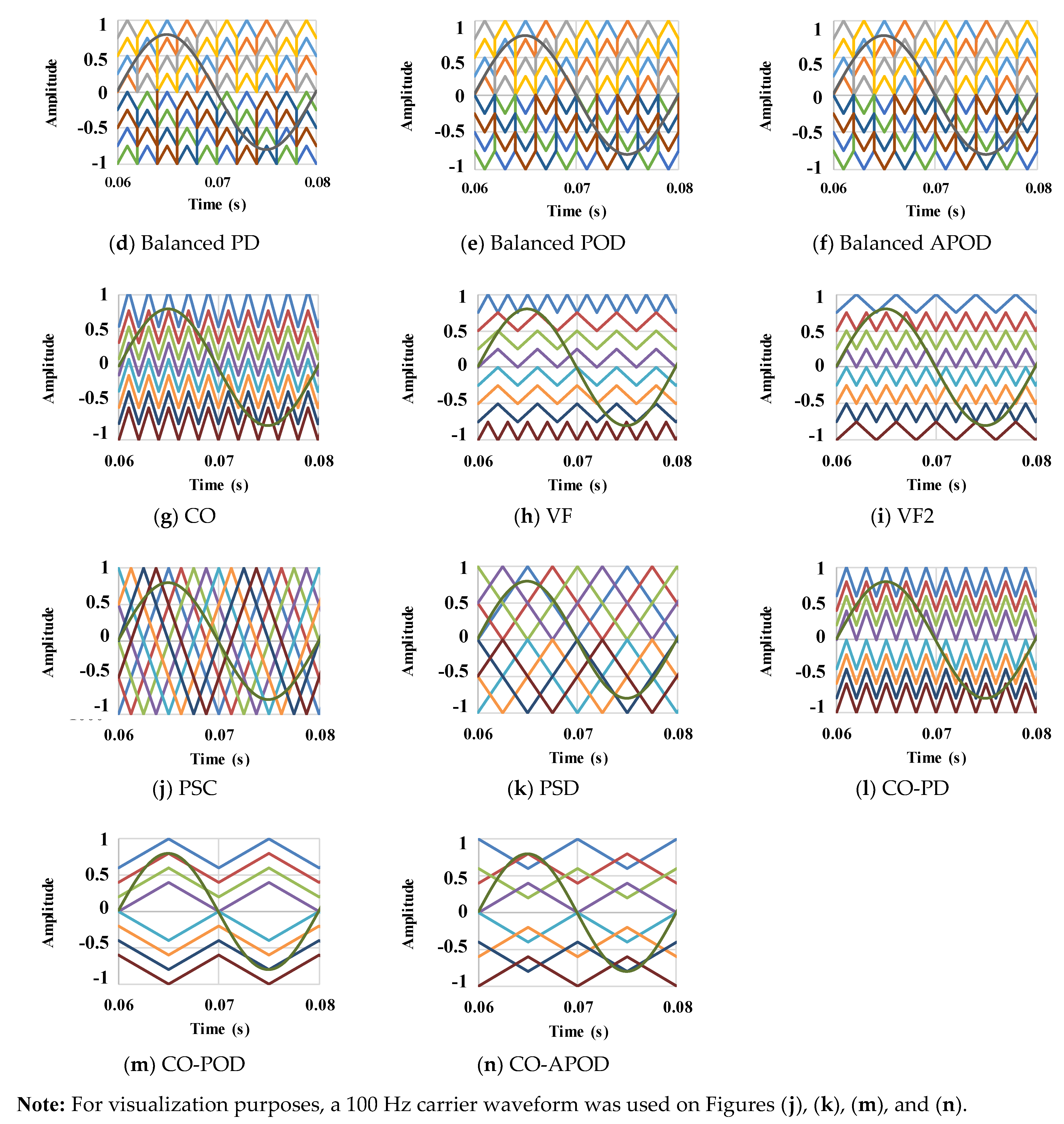
Regarding the PD technique, the carrier waves are synchronized with the same phase angle, as represented in the Figure 11a. In turn, the POD technique presents carrier waves with symmetry to the zero-reference axis. That is, the positive value carrier waves are synchronized with a phase angle of 0°, while the negative value carrier waves are synchronized with a phase angle of 180°, as illustrated in Figure 11b. Finally, for the APOD technique, all carrier waveforms are 180° lagged alternately, as shown in Figure 11c. Note that, due to the alternating arrangement in the carrier waveforms, the modulation presents symmetry in relation to the zero-reference axis. In the following three figures is represented an approach in order to mitigate the previously mentioned imbalance problems, which are balanced PD in Figure 11a, balanced POD in Figure 11b, and balanced APOD in Figure 11c. This approach consists of varying the average value of the carrier waves at each switching period [221]. This permutation technique can be integrated with any level shifting technique. In this way, in short periods of time, it is possible to balance the contribution of each module in the synthesized waveform. Note that the permutation must be performed along all levels, and not only to the adjacent levels. Otherwise, with the greater the number of levels, and if the permutation is performed only on adjacent modules, the imbalance will be still evident.

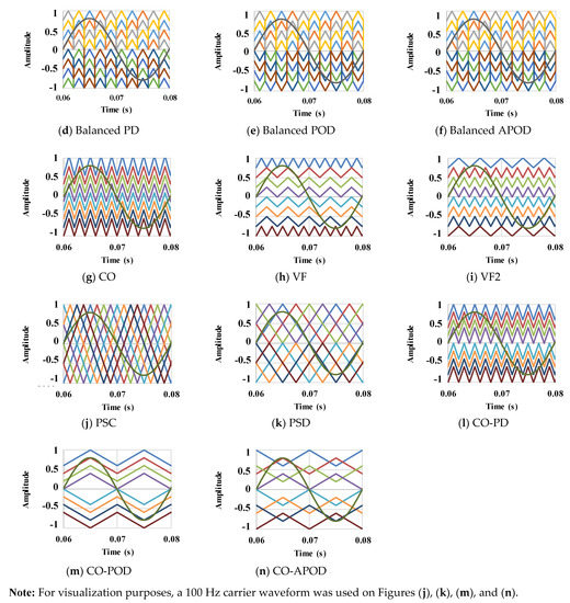
Figure 11.
Illustration of the carrier and modulation wave forms for different PWM techniques: (a) PD, (b) POD, (c) APOD, (d) Balanced PD, (e) Balanced POD, (f) Balanced APOD, (g) CO, (h) VF, (i) VF2, (j) PSC, (k) PSD, (l) CO-PD, (m) CO-POD, (n) CO-APOD.
Carrier overlapping (CO) appears as another group of techniques that, as the name implies, consists of overlapping the carrier waves. The carrier waves have the same frequency, angle, and amplitude, varying the average value. The amplitude value of each carrier wave can be defined by the ratio of twice the maximum peak-to-peak value of the carrier wave spectrum by the number of carrier waves, N, needed, plus one, as represented in Equation (1). That is, analyzing the example shown in Figure 11g, if the maximum value is 2000 and eight carrier waves are needed, the amplitude value should be 444. In turn, the overlap value represents half of the amplitude, it being 222 in the exemplified case.
Due to the overlap of the carrier waves, the modulating wave intersects more often with the carrier waves, minimizing the dispersion of the harmonic content. Thus, with the correct sizing of the modulation index, it is possible to obtain an improvement in system performance when compared to other modulation techniques. The study presented in [101] aids in calculating the better modulation index for MLCs. In the case of the NPC converter with three levels, this characteristic is evident for a modulation index below 70%. In turn, for an index higher than 80%, the harmonic content is similar. Despite the existence of this modulation technique in the literature, there is no scientific content describing its practical implementation.
In cascaded MLC applications, when the output voltage reaches maximum values, the bus voltages of the peripheral modules tend to oscillate [65]. By adopting a different switching frequency in these submodules, it is possible to minimize the voltage ripple in the capacitors, consequently improving the quality of the output waveform. The variable frequency (VF) PWM technique whose carrier waves from the peripheral submodules have higher frequencies is exemplified in Figure 11h.
In turn, in converters such as the NPC, the IGBT devices located at the periphery have a higher switching frequency than the internally located IGBT devices. Consequently, an analogous variable frequency 2 (VF2) approach is required in order to equalize the switching losses [65]. As such, the internal carrier waves have a higher frequency than the peripheral carrier waves, as exemplified in Figure 11i, making all the IGBT devices that make up the topology able to switch at similar frequencies. An experimental result of a five-level NPC using the VF2 can be found in [222].
In general, with the implementation of carrier waves with different frequencies, depending on each specific application, it is possible to reduce the output harmonic spectrum through harmonic cancellation.
4.2. Phase-Shift Carrier PWM Technique
The phase-shift carrier (PSC) PWM technique is one of the most widely used in power electronics applications. One of the reasons lies in its easy implementation, with digital signal controllers (DSC) with their own registers for phase angle control and synchronization with other carrier waves. The carrier waves of the PSC PWM technique share the same amplitude, frequency, and mean value. The carrier waves have a phase angle between them of 2π/n, as represented in Figure 11j. Knowing that n represents the number of arms and that in an MLC consisting of four cascaded full-bridge, there are right semiconductor arms, the carrier waves would be 45° lagged between them.
By analyzing Figure 11j, it is possible to predict that the modulating wave will intercept the carrier waves more often. As such, each submodule will contribute to the generation of the output waveform in a more similar way. That is, each submodule will exhibit similar operating powers and outputs. In cascaded applications, the voltage ripple of the buses will be similar. These characteristics enhance the concept of modularity. However, the PSC technique is not suitable for topologies such as NPC since it has a lower sensitivity and effectiveness to DC bus voltage ripples when compared to the VF technique [65].
4.3. Hybrid Carrier PWM Technique
Hybrid techniques consist of the fusion of different techniques, enhancing the most advantageous characteristics of each one. Some examples of combinations are phase-shift disposition (PSD), carrier overlapping disposition (COD), carrier overlapping phase disposition (CO-PD), carrier overlapping opposition disposition (CO-POD), and carrier overlap-alternate phase opposition disposition (CO-APOD). It should be mentioned that the hybrid technique has the major restriction of synthesizing M odd output voltage levels [65].
Combining the PSC and PD techniques, the PSD technique capable of controlling an MLC with M output voltage levels can be obtained. By analyzing Figure 11k, it is possible to see the existence of (M-1)/2 carrier waves above the zero-reference line. These waves have the same amplitude, frequency, and average value but have different phase angles. The remaining (M-1)/2 carrier waves have a symmetric average value, being therefore below the zero-reference line. Consequently, it is possible to see that there is symmetry to the zero-reference axis. The harmonic content resulting from the PSD technique is concentrated in fc(M-1)/2, fc being the frequency of the carrier waveform. As such, it is simple to eliminate the harmonic content resulting from IGBT switching through passive filters tuned to this frequency. In [65], the authors state that in five-level NPC (5L-NPC) applications with a modulation index higher than 70%, this modulation technique presents lower switching losses compared to PD, POD, APOD, CO, PSC, and COD.
Combining the CO technique with the level shift techniques, the COD technique can be obtained. This technique always has two groups of (M-1)/2 carrier waves. Depending on the technique used for level shift, different arrangements can be obtained. The carrier waves have the same frequency and amplitude, with the average value imposed by the CO technique and the phase angle by the PD technique.
The combination of the PD and CO technique gives the CO-PD technique, where the carrier waves have the same amplitude, frequency and phase, but different average values, as exemplified in Figure 11l. In turn, combining the POD and CO techniques produces the CO-POD technique, where the carrier waves below the zero-reference axis are 180° out of phase with respect to the upper carrier waves, as can be seen in Figure 11m. Finally, combining the APOD and CO techniques produces the CO-APOD technique, as illustrated in Figure 11n.
Note that the y axis shown in Figure 11 represents the amplitude of the carrier and modulator waves. In practical implementation, the amplitude values of each wave should be adjusted according to the registers of the peripheral used as PWM. Nevertheless, the values must be shifted vertically in order to always obtain positive values. It should be mentioned that there are DSCs, such as those of the C2000 family from Texas Instruments, as dedicated registers for easy configuration of the carrier wave lags. However, the vertical displacement of the waves does not present the same ease, and sometimes, conditions are implemented in order to adapt the modulating wave to obtain effects similar to the vertical displacement of the carriers. A comparative and informative study on how to implement these modulation techniques in C language would be interesting and a strong contribution to the development of modular and multilevel power electronics solutions.
4.4. Other Modulation Techniques
Other modulation techniques can be found in the literature, namely square wave modulation. This technique is mostly used in MMC applications with SST, allowing for the minimization of the value of the capacitance of the DC bus capacitors [223], the reduction in the dv/dt stress of the semiconductors [224], the optimization of the transformer flux density [225], the minimization of core losses, and the maximization of energy transfer on the transformer [226].
Modular and multilevel solutions, such as the MMC and MMCC, are particularly adapted for high-voltage and high-power applications due to the aforementioned intrinsic characteristics. However, in order to achieve a minimum DC bus voltage, it is necessary to connect several submodules. The combination of different submodules with slight differences in capacitance values, parasitic impedances, PWM techniques used, and different IGBT conduction times leads to different capacitor charge and discharge patterns. Some PWM techniques can minimize this problem, but, ultimately, balancing algorithms are needed. Consequently, not only does the DC bus regulation algorithm increase in complexity, but more signal acquisition hardware is needed with the increase in the number of submodules. It should be mentioned that the increase in this complexity leads to a longer processing time in the centralized microcontroller. In order to increase the efficiency of the MMC and MMCC, it is necessary to correctly size the number of submodules and the modulation indices, as well as to implement the correct DC bus balancing algorithms.
Regarding the balancing algorithms, they use redundant states in order to combine the output synthesized level of the MMC with the balancing of the capacitors’ voltages. The alternation of the operating states of the submodules in order to balance the capacitors voltages is one of the most-used solutions in MMCs and MMCCs. The performance of a balancing algorithm for a STATCOM composed of seven cascaded full-bridge converters for each phase of the power grid and with an unbalanced DC bus at the beginning is presented in [227].
In applications focused on very high voltage, with hundreds of submodules, the complexity and processing time can reduce the effectiveness of the control. On the other side, the voltage contribution of each submodule is relatively low. Then, the desired output voltage can be synthesized by adding up an appropriate number of submodules according to the phase angle of the reference voltage. This is the degree of freedom allowed in the development of sorting algorithms for the selection of the submodules to be in service in each time interval. Reference voltage level, submodule voltage, capacitor voltage balancing, etc. are parameters used by the sorting algorithms to select the submodules to be connected. As such, capacitor voltage prediction strategies of a half-bridge MMC [228] (saving 2/3 of the time compared to the commonly implemented quicksort algorithm for an arm with 100 submodules), the odd–even sorting technique implemented in FPGA [229] or a full-bridge MMC [230], techniques based on the grouping and sorting of MMCs [231] with decentralized control [232], the “Tortoise and the Hare” sorting method [233], a fundamental frequency with staircase modulation [234] or with a PSC [235] sorting algorithm for MMC, and a current sensorless sorting and selection algorithm [236] have been studied and implemented. Different balancing techniques were also studied in an MMC based on SST [237].
The SVM technique appears as another technique for controlling the semiconductors that make up the MLC. This technique consists of different sectors, which make up a switching state, and the algorithm will determine the sector that better eliminates the output operation error. In three-phase MLC applications, the number of redundant states increases substantially and is indicated for these systems. However, and despite the good characteristics for single-phase systems, namely determining the best operating status and keeping the DC bus regulated, there is still a gap in the contribution of this system. Contributions at the level of implementation in programming language and migration to a single-phase system depending on the chosen topology are necessary. Although the SVM technique is beyond the scope of this article, it is possible to find in the literature the SVM technique implemented in an MMC consisting of FCMC [238], a simplified SVM for a five-level MMC [239], an SVM implemented for a three-level NPC [240], and an approach for single-phase applications [241,242].
5. Simulation Results of PWM Techniques Applied on a Full-Bridge Cascade Converter
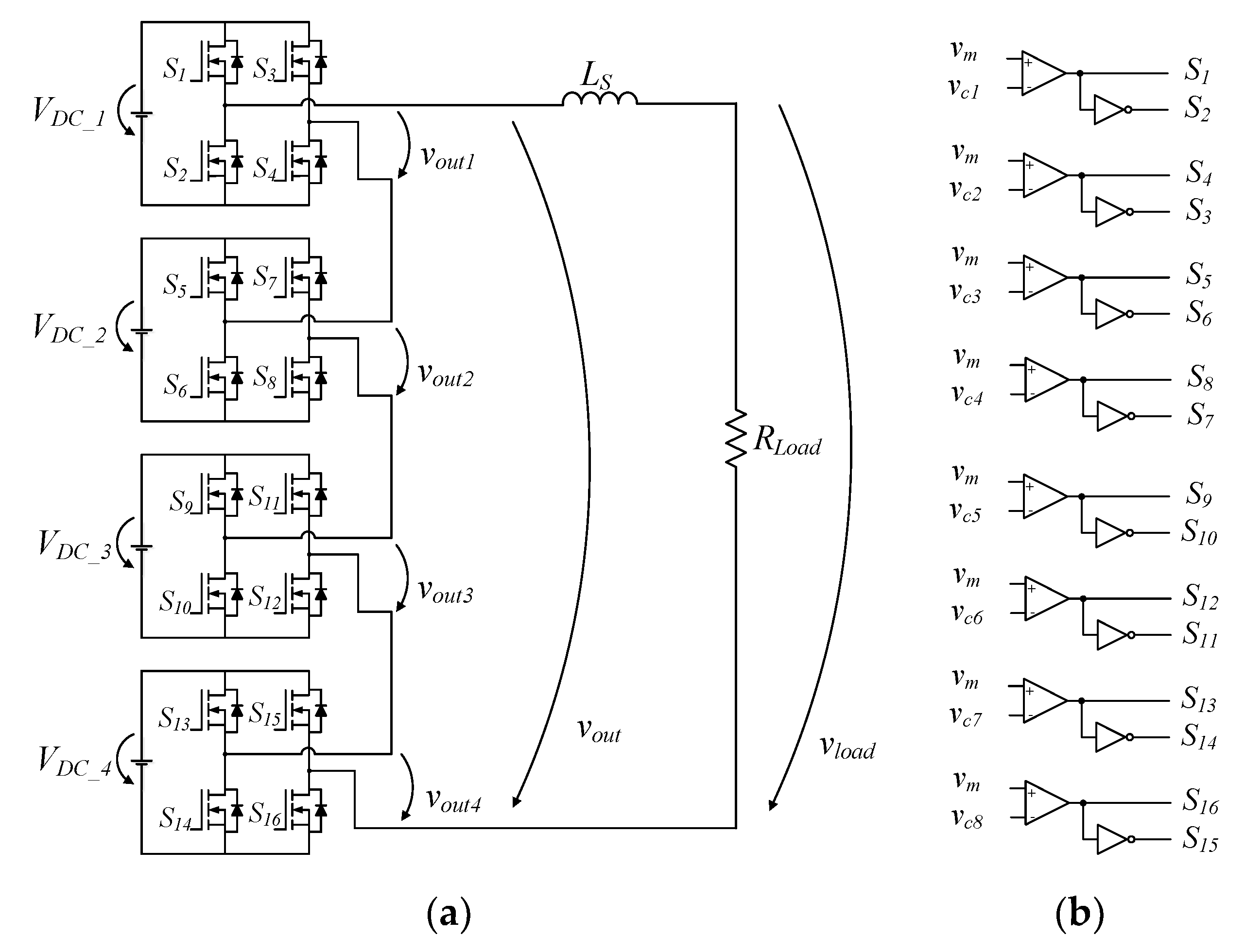
In this topic, a comparative analysis of different PWM modulation techniques based on computer simulations is performed. The simulation model was implemented in PSIM software, and the main parameters used are presented in Table 4. The Semikron IGBT with the reference SKM100GB12V was considered in order to obtain some real parameters for the IGBT model used in simulation. The MLC topology adopted was the cascaded four full-bridges submodules, being the electrical schematic shown in Figure 12a. A DC-source was connected to the DC bus of each submodule, keeping the bus voltage constant. The PWM signal sequence and logic are illustrated in Figure 12b. It should be mentioned that the modulation index and a current control algorithm should be adjusted for the final application. Some examples of control algorithms can be based on integral proportional, resonant proportional, and dead-beat predictive controls, among others [243,244]. The authors of [77] present the integration of some control methods in MLCs, namely positive and negative sequence detectors and current control, zero sequence current control, DC voltage equalization, circulating current compensation, and others.

Table 4.
Main simulation parameters.

Figure 12.
Electrical schematic of the (a) cascaded full-bridge and (b) PWM control circuit.
With this configuration of four submodules composed of full-bridges topology, it is possible to obtain 256 redundant states, with each voltage level having a limited number of states, as shown in Table 5. By analyzing Table 5, it is possible to verify that there is only one state to generate 4 VDC at the vout, when the four submodules are generating VDC. On the other hand, to generate 3 VDC, there are right states: when three of the submodules are generating VDC and a single submodule is generating 0. As there are two possibilities of generating 0 and four submodules, it is possible to obtain the right states. Continuing with the analysis, to generate 2 VDC, there are twenty-eight redundant states that are essentially divided into two conditions: (i) when three submodules generate 3 VDC and another submodule generates −VDC and (ii) when two submodules generate 2 VDC and the others are generating 0. Within these conditions, there are four combinations to generate 3 VDC − VDC and twenty-four combinations to generate 2 VDC + 0 + 0. In turn, to generate VDC, there are fifty-six states, which can be divided into two conditions: (i) two submodules to generate 2 VDC, one generating −VDC and the fourth submodule generating 0 and (ii) one submodule generating VDC and the remaining three submodules generating 0. Regarding the first condition, there are twelve possible combinations to generate 2 VDC − VDC + 0. Once there are two conditions to generate 0, the number of states is doubled, thus accounting for twenty-four states for 2 VDC − VDC + 0. In turn, for the VDC + 0 + 0 + 0 condition, there are thirty-two states. Finally, for the 0 state, it is possible to count fifty-four states, which can be divided into three conditions: (i) when two submodules generate 2 VDC and the remaining two submodules are generating −2 VDC; (ii) when a submodule is generating VDC, one submodule is generating −VDC, and the remaining two submodules are generating 0; and (iii) all submodules are generating 0. For the first condition, there are six possibilities for generating 2 VDC − 2 VDC. Regarding the second condition, there are twelve states to generate VDC − VDC + 0 + 0. As there are two possibilities of 0 VDC, the number of states is replicated to twenty-four. Regarding the last group, it is possible to count twenty-four states to generate the condition 0 + 0 + 0 + 0.

Table 5.
Redundant states for the cascaded four submodules full-bridge.
For negative values, the number of states is equal to the number of positive values, changing the condition to generate − VDC.
5.1. Basic Level-Shift PD, POD, and APOD PWM Techniques
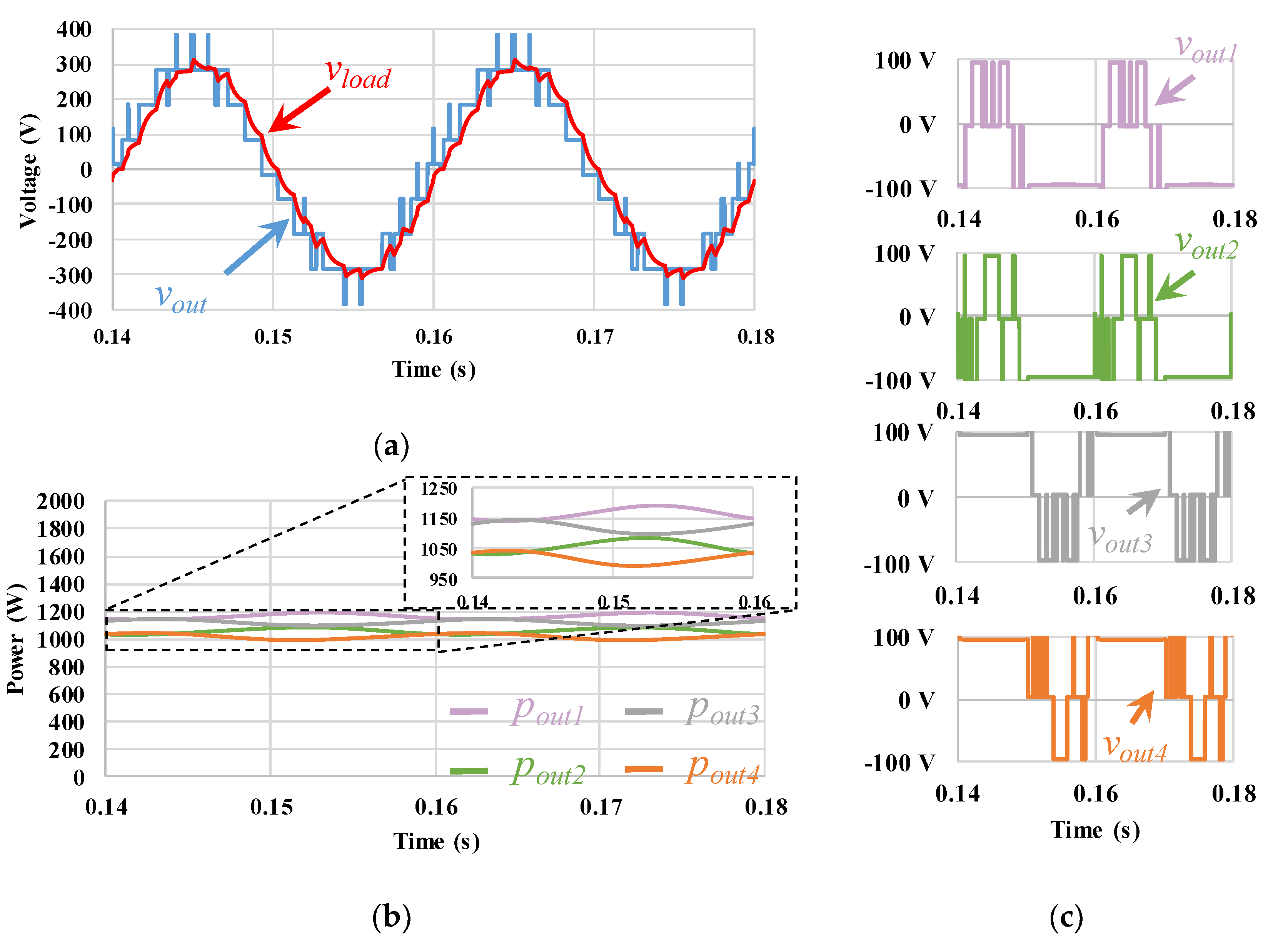
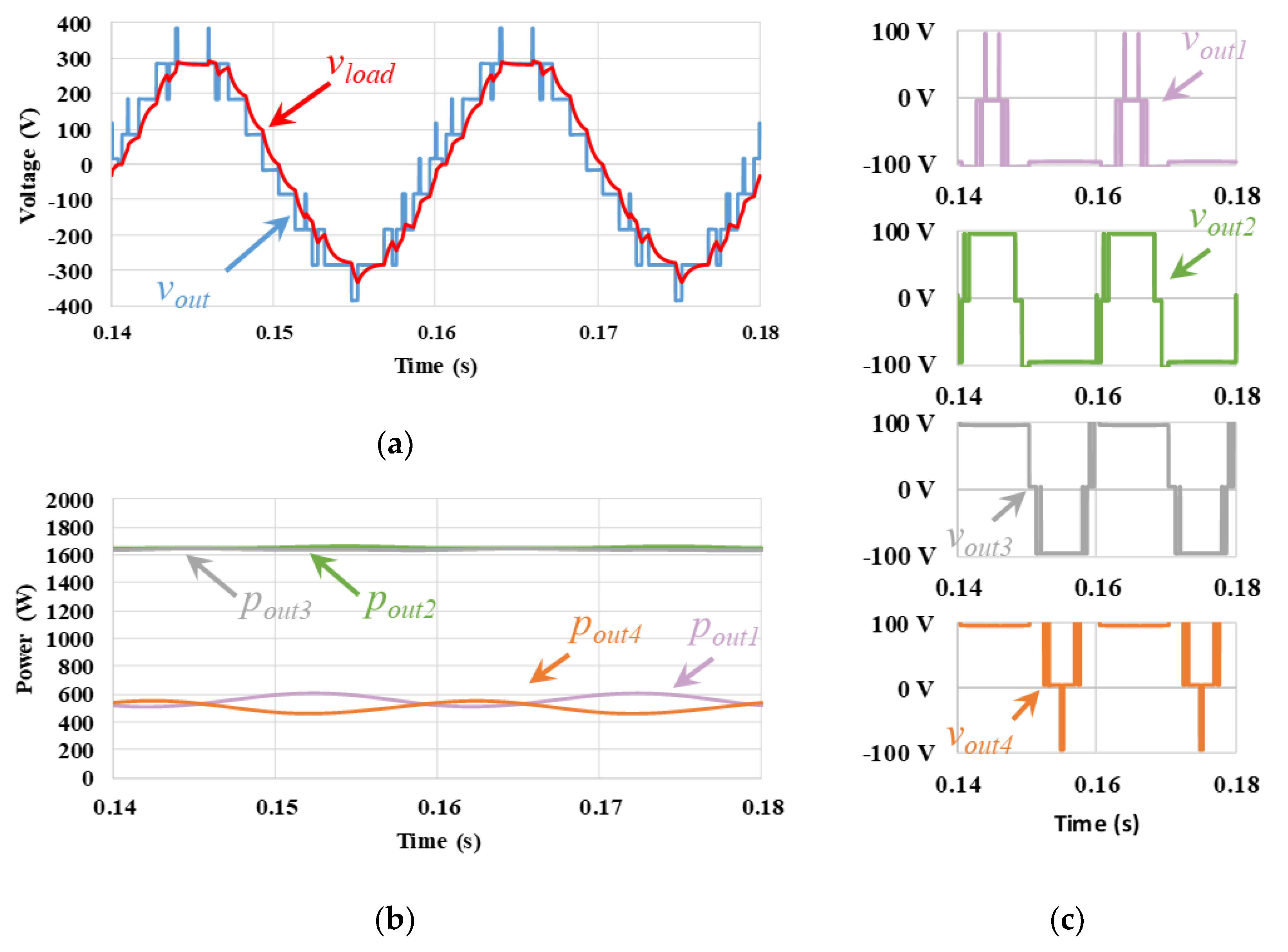
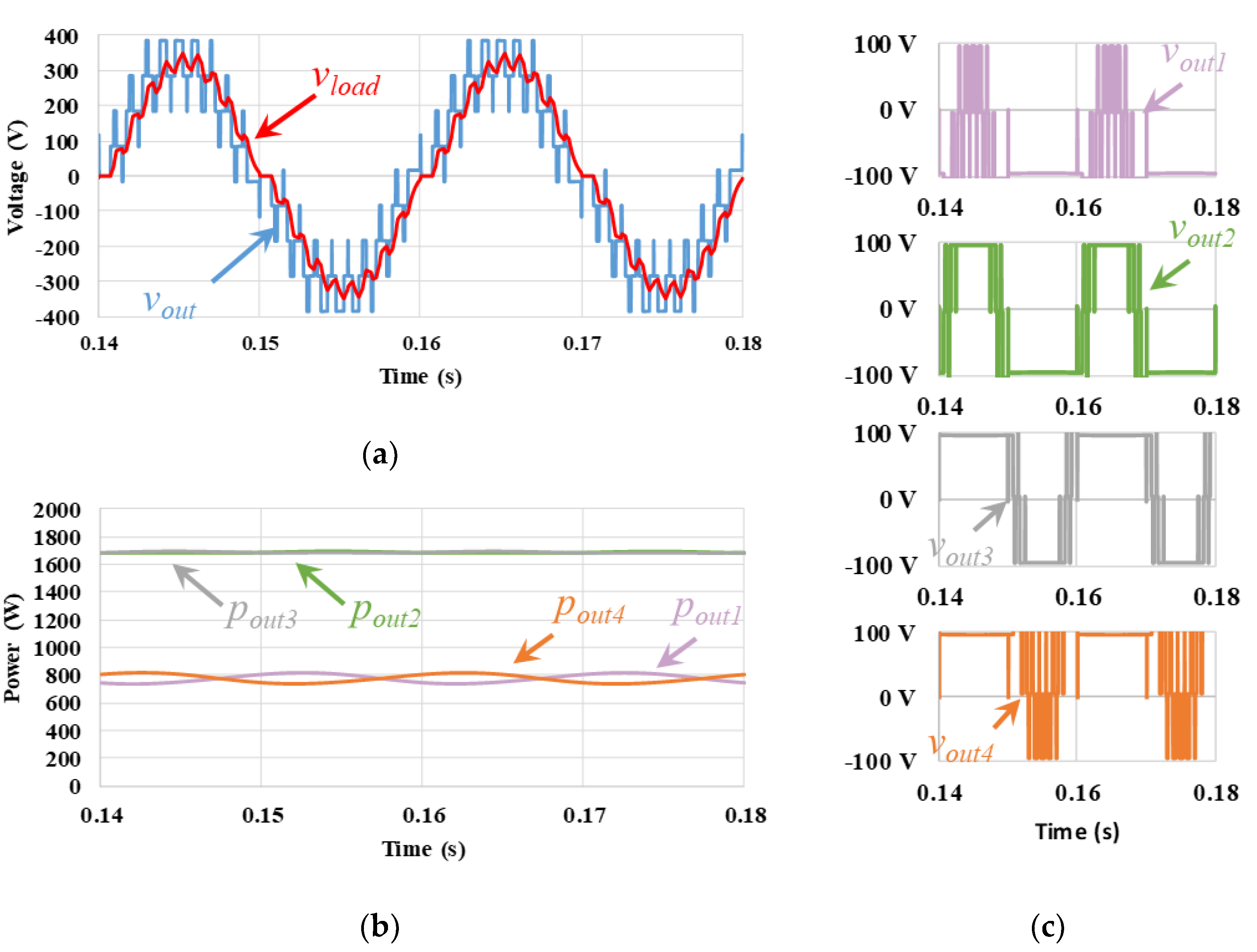
The first PWM technique implemented for analysis was the PD, and the results are shown in Figure 13. In Figure 13a are illustrated the MLC output voltage waveform, vout, and the voltage waveform at load, vload. In analyzing the waveforms, it is possible to see that vout does not present symmetry in relation to the zero-reference axis. That is, the positive semi-cycle presents a waveform not symmetrical in relation to the negative semi-cycle. In Figure 13b are represented the power variations of each submodule over two cycles. It should be mentioned that the submodules have an oscillating power of 50 Hz, with a 180° delay with the complementary submodule. That is, pout3 is 180° lagged in relation to pout2, and pout4 is 180° lagged in relation to pout1. It should also be mentioned that, considering the pairs pout2 with pout3 and pout1 with pout4, they present slightly different average power values due to the asymmetry of the carrier waveforms. It is also possible to see the existence of submodules contributing with a power 3.3 times higher than other submodules. This fact is verified in Figure 13c, where each submodule presents a different pattern in the output voltage (vout1, vout2, vout3, and vout4). It should be noted that these differences in patterns cause each submodule to present different and unique powers.
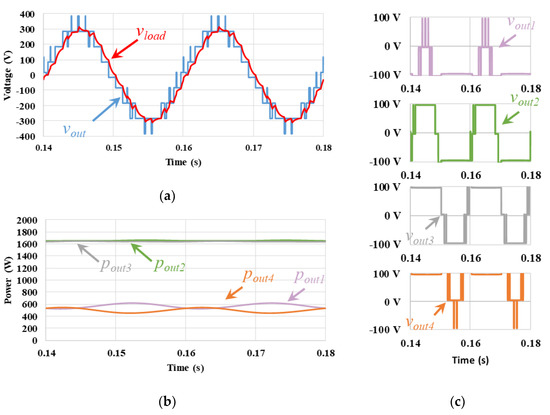
Figure 13.
Simulation results of the PD PWM technique: (a) output voltage of the cascaded MLC, vout, and load voltage, vload; (b) output power on each submodule (pout1, pout2, pout3, pout4); (c) output voltage on each submodule (vout1, vout2, vout3, vout4).
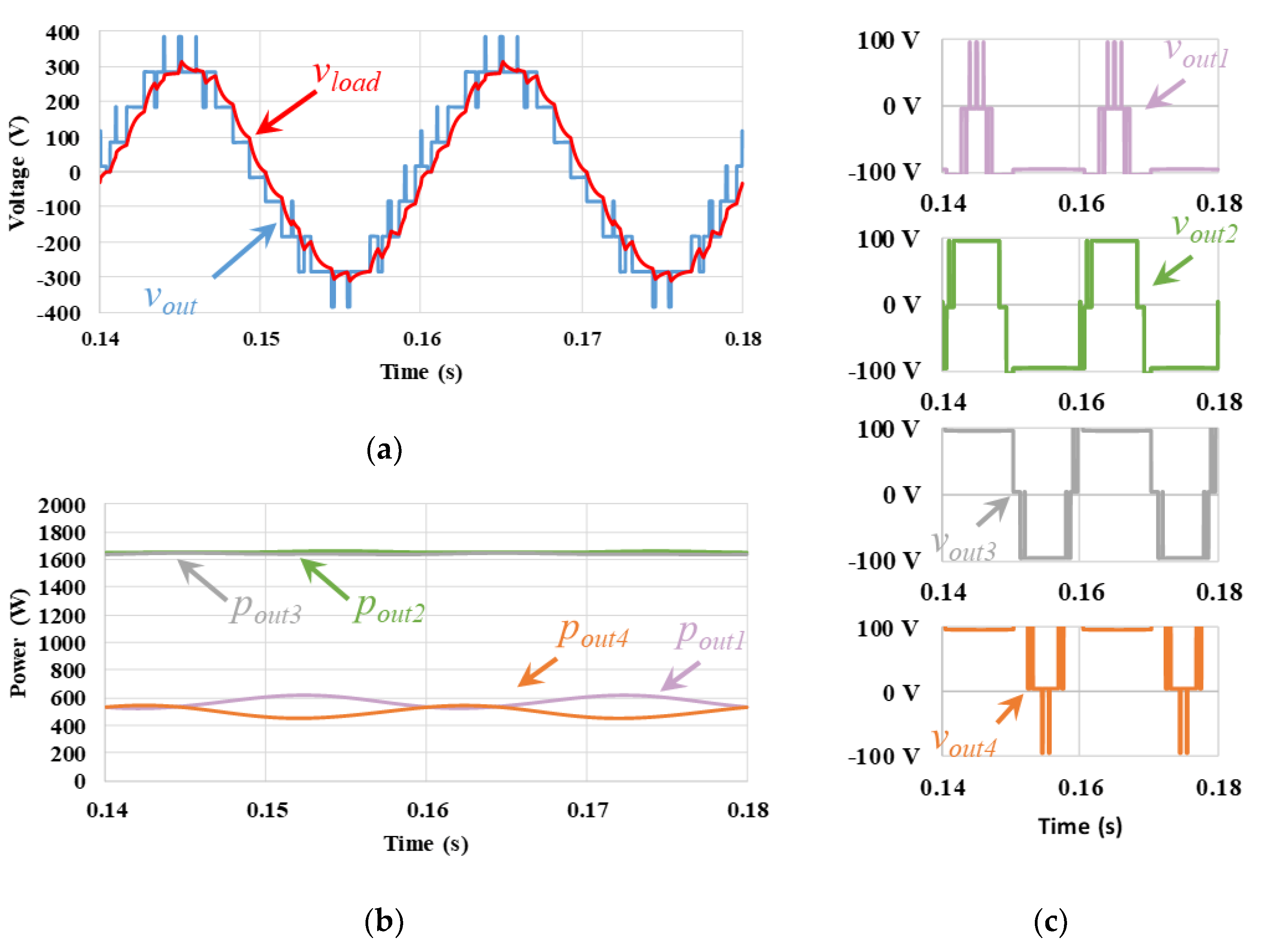
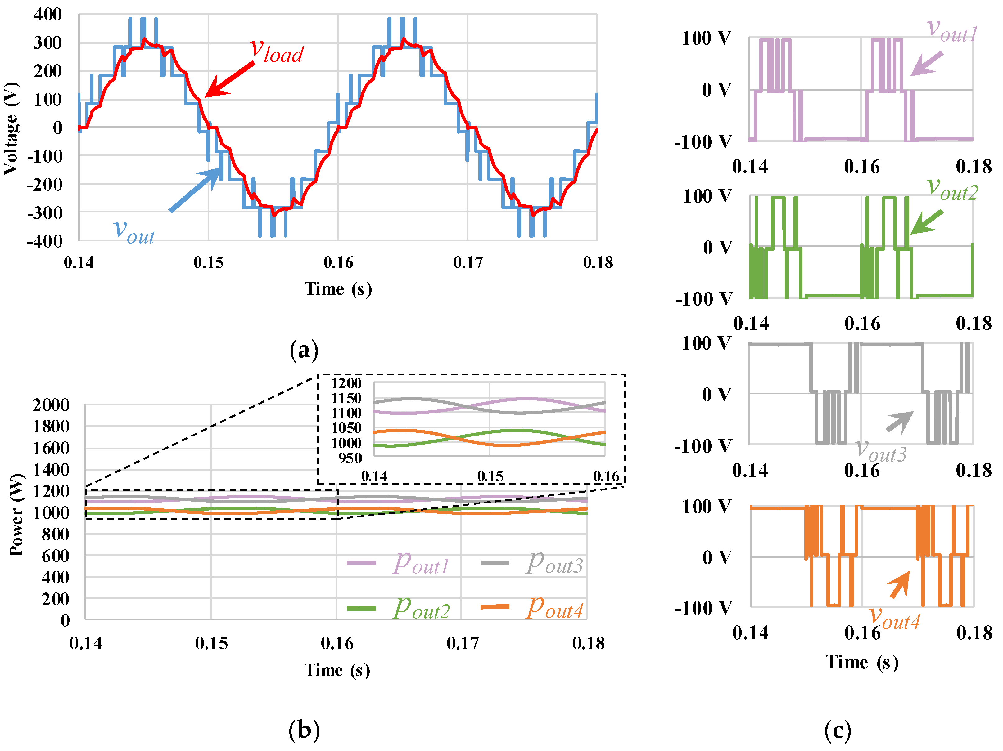
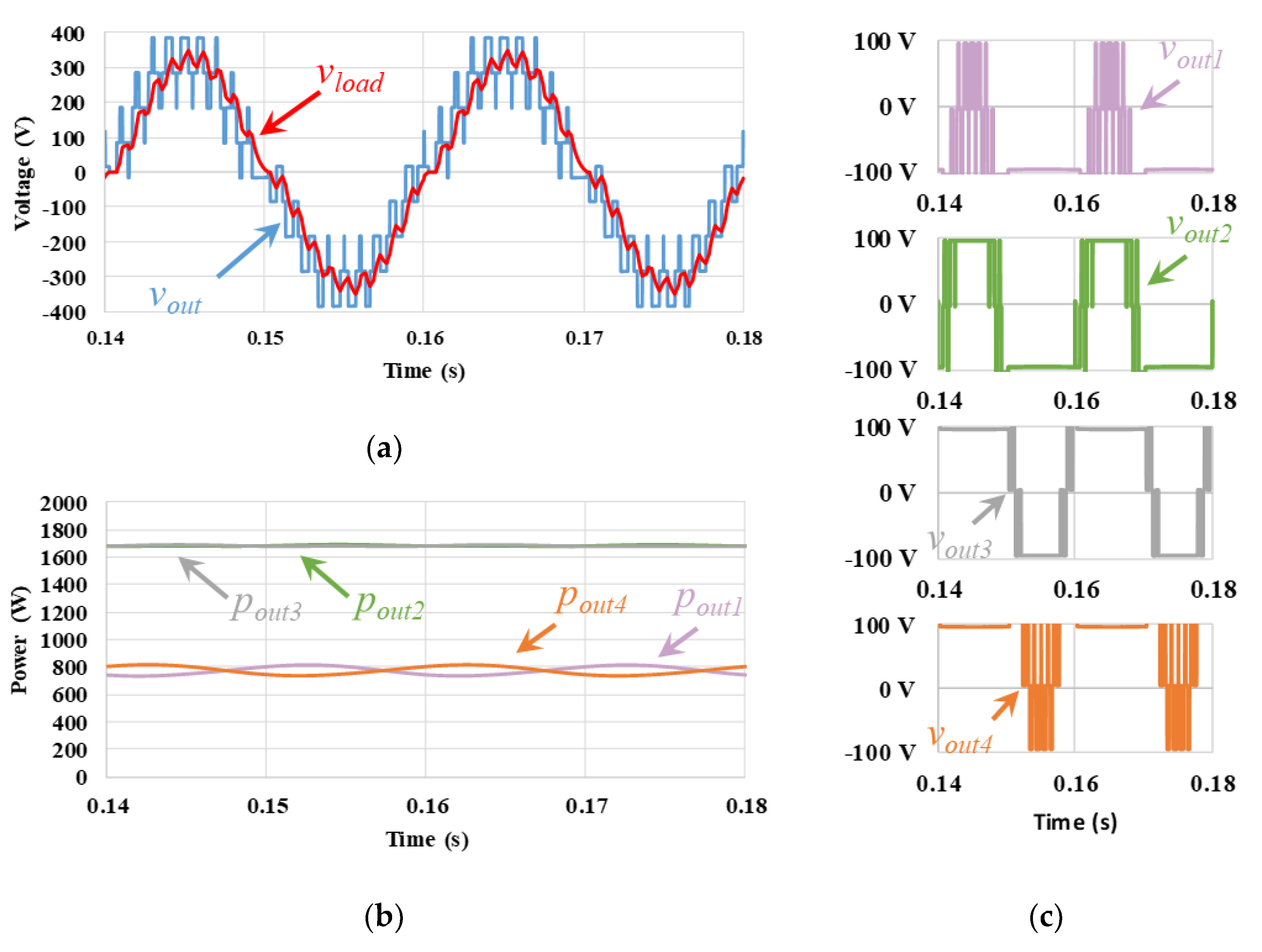
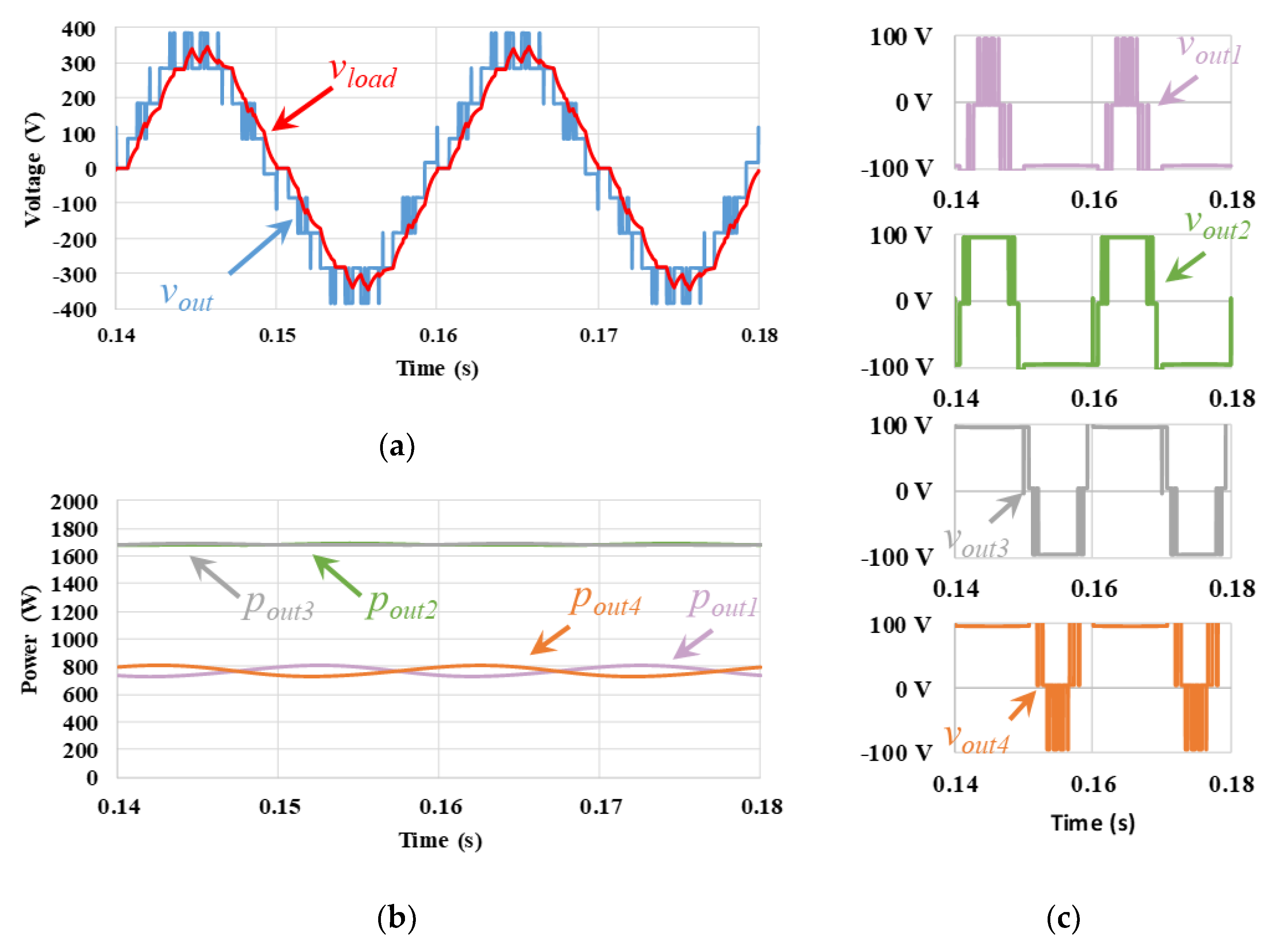
The next technique implemented was the POD, and the results are presented in the Figure 14. By analyzing the vout and vload waveforms in Figure 14a, it is possible to see that there is a symmetry with respect to the zero-reference axis. This fact is due to the symmetry of the carrier waveforms, as mentioned before. Figure 14b shows the power variation of each submodule over two cycles. It should be mentioned that the submodules have an oscillating power of 50 Hz, with a 180° delay with the complementary submodule. That is, pout3 is 180° lagged in relation to pout2, and pout4 is 180° lagged in relation to pout1. It should also be mentioned that the pairs pout2 with pout3 and pout1 with pout4 present similar average power values due to the asymmetry of the carrier waveforms. It is also possible to see that the power distribution among the different submodules is not uniform, with some submodules contributing 3.1 times more power. This fact is seen in Figure 14c with submodules having different output voltage patterns (vout1, vout2, vout3, and vout4). However, it should be mentioned that the symmetry of the carrier waves causes a parity in the system, and there is a complementary submodule with a similar voltage and power pattern. Despite this parity, the POD technique still has low modularity.
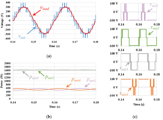
Figure 14.
Simulation results of the POD PWM technique: (a) output voltage of the cascaded MLC, vout, and load voltage, vload; (b) output power on each submodule (pout1, pout2, pout3, pout4); (c) output voltage on each submodule (vout1, vout2, vout3, vout4).
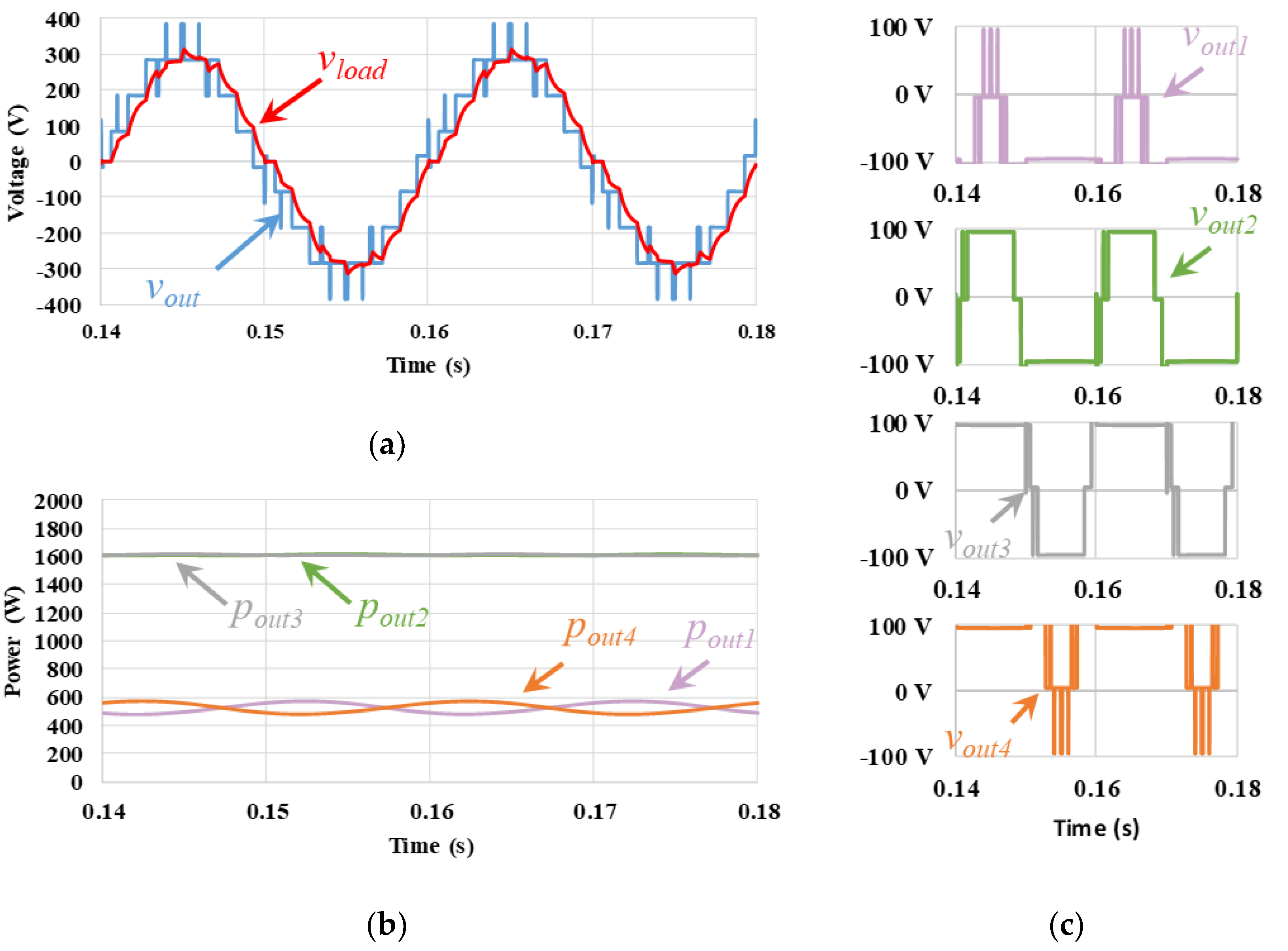
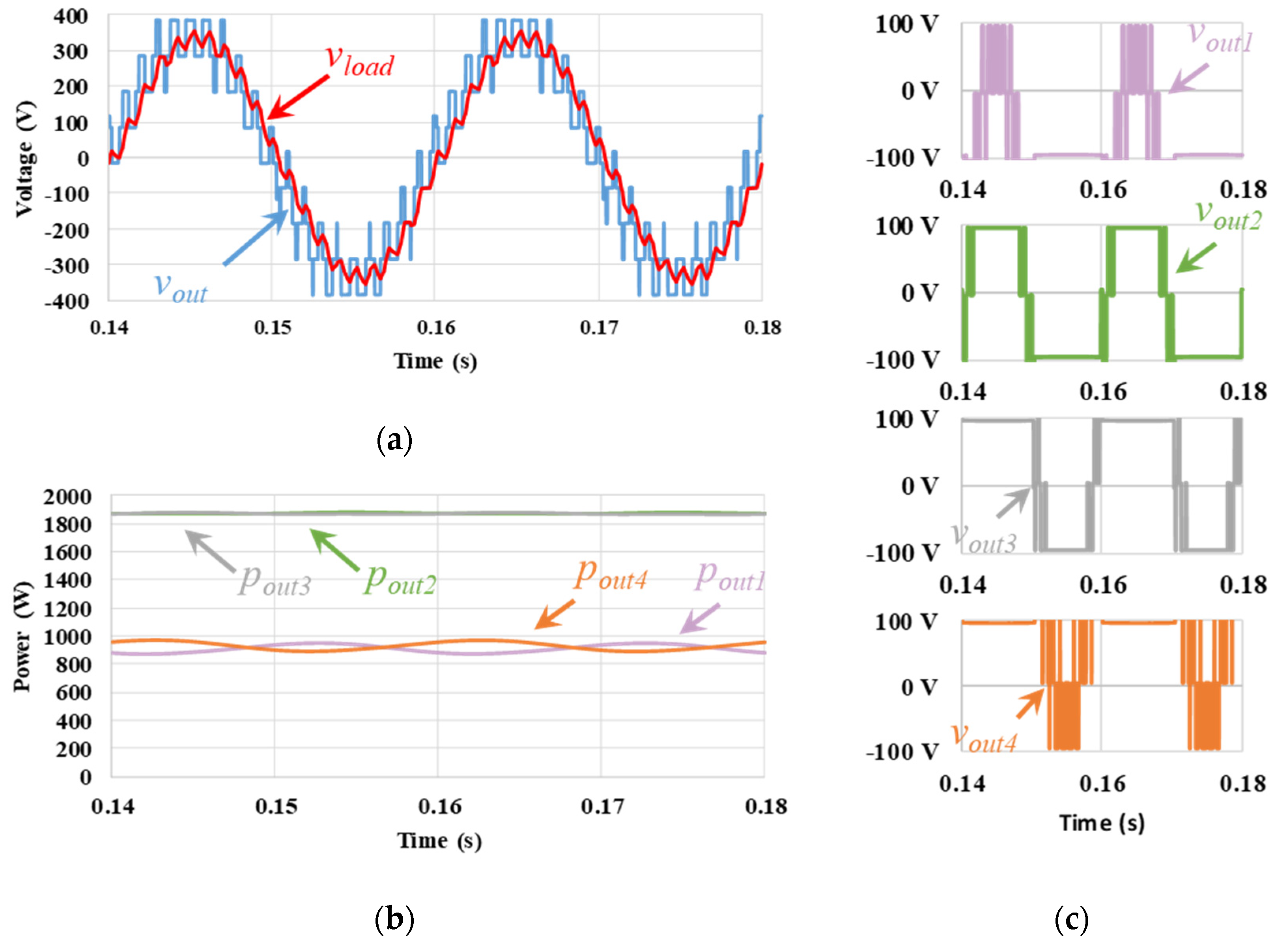
Regarding the APOD technique, the simulation results are shown in Figure 15. In Figure 15a are illustrated the vout and vload waveforms. Analyzing the waveforms, it is possible to see that vout presents symmetry in relation to the zero-reference axis. In Figure 15b is represented the variation of power in each submodule over two cycles. It should be mentioned that the submodules have an oscillating power of 50 Hz, with a 180° delay with the complementary submodule. That is, pout3 is 180° lagged in relation to pout2, and pout4 is 180° lagged in relation to pout1. It should also be mentioned that the pairs pout2 with pout3 and pout1 with pout4 present similar average power values due to the symmetry of the carrier waveforms. It is also possible to see that the power distribution for each submodule is not uniform, with some submodules contributing 3.1 times more power. Once again, this fact is verified with the analysis of Figure 15c, where each submodule presents a different pattern in the output voltage (vout1, vout2, vout3, and vout4).
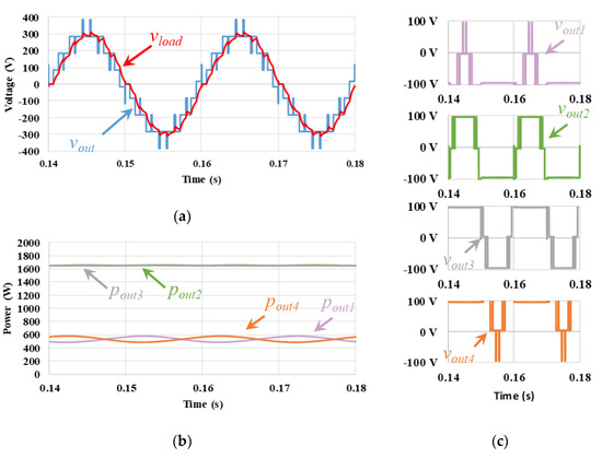
Figure 15.
Simulation results of the APOD PWM technique: (a) output voltage of the cascaded MLC, vout, and load voltage, vload; (b) output power on each submodule (pout1, pout2, pout3, pout4); (c) output voltage on each submodule (vout1, vout2, vout3, vout4).
5.2. Power Balancing Level-Shift PD, POD, and APOD PWM Techniques
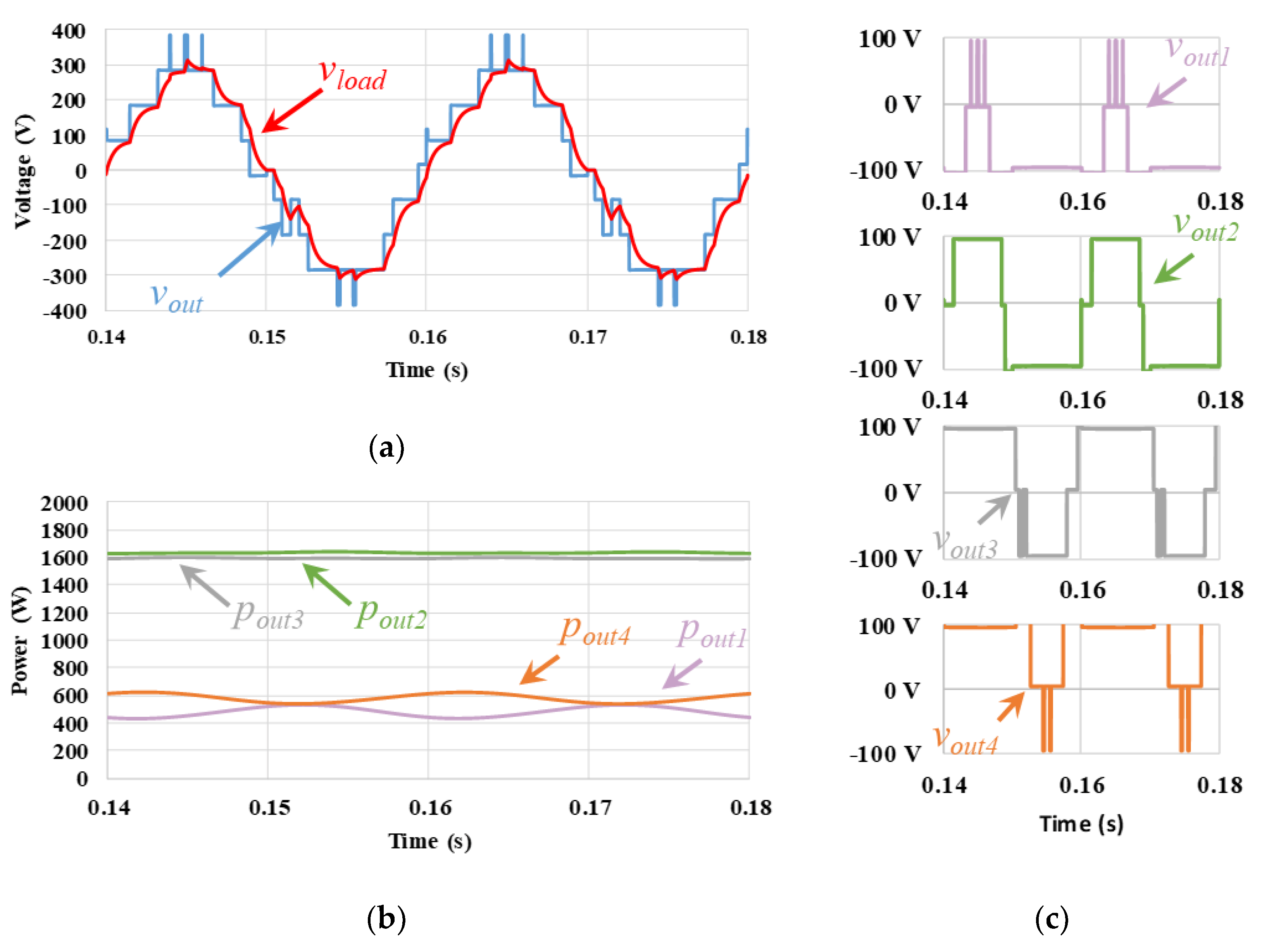
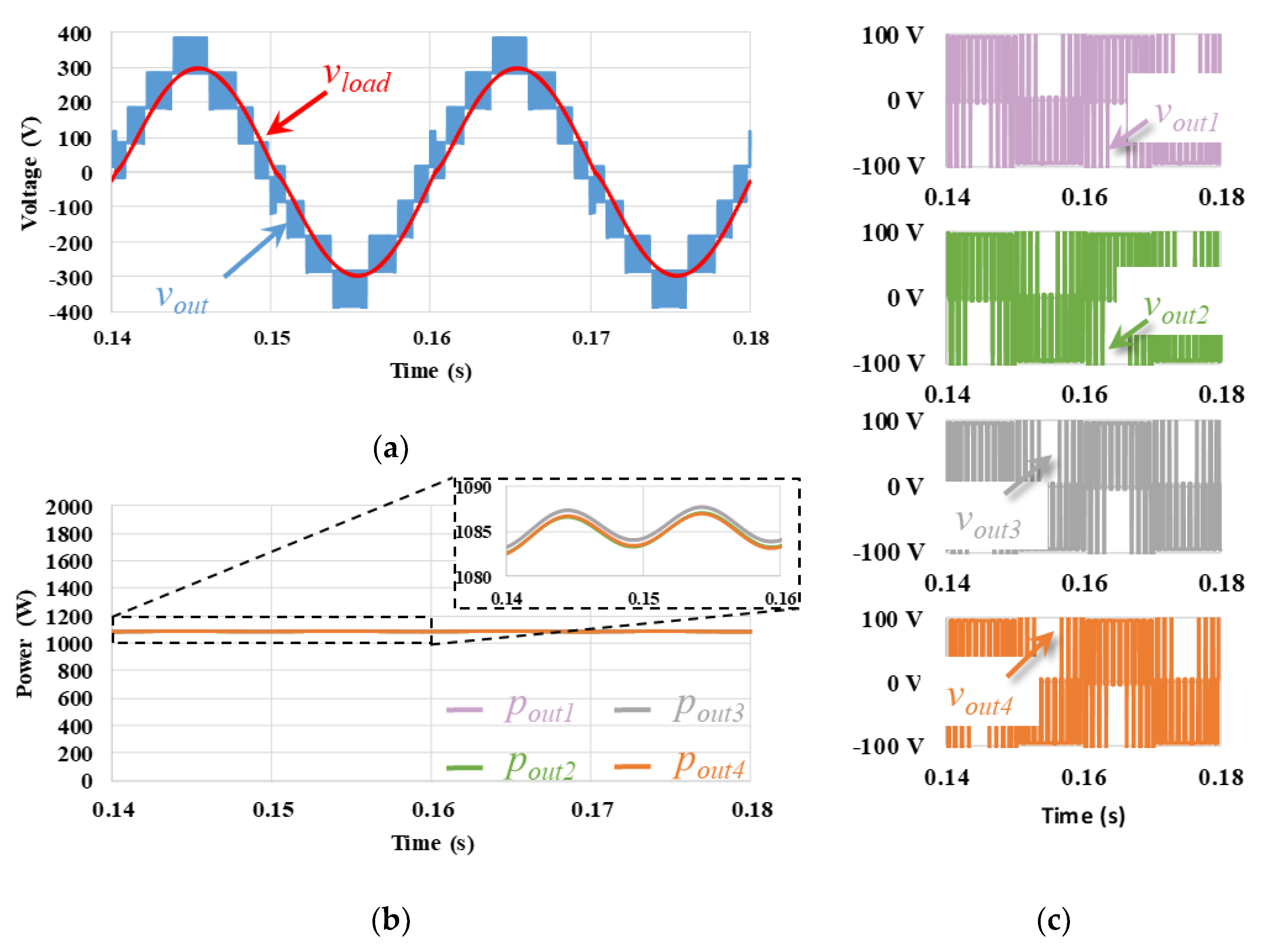
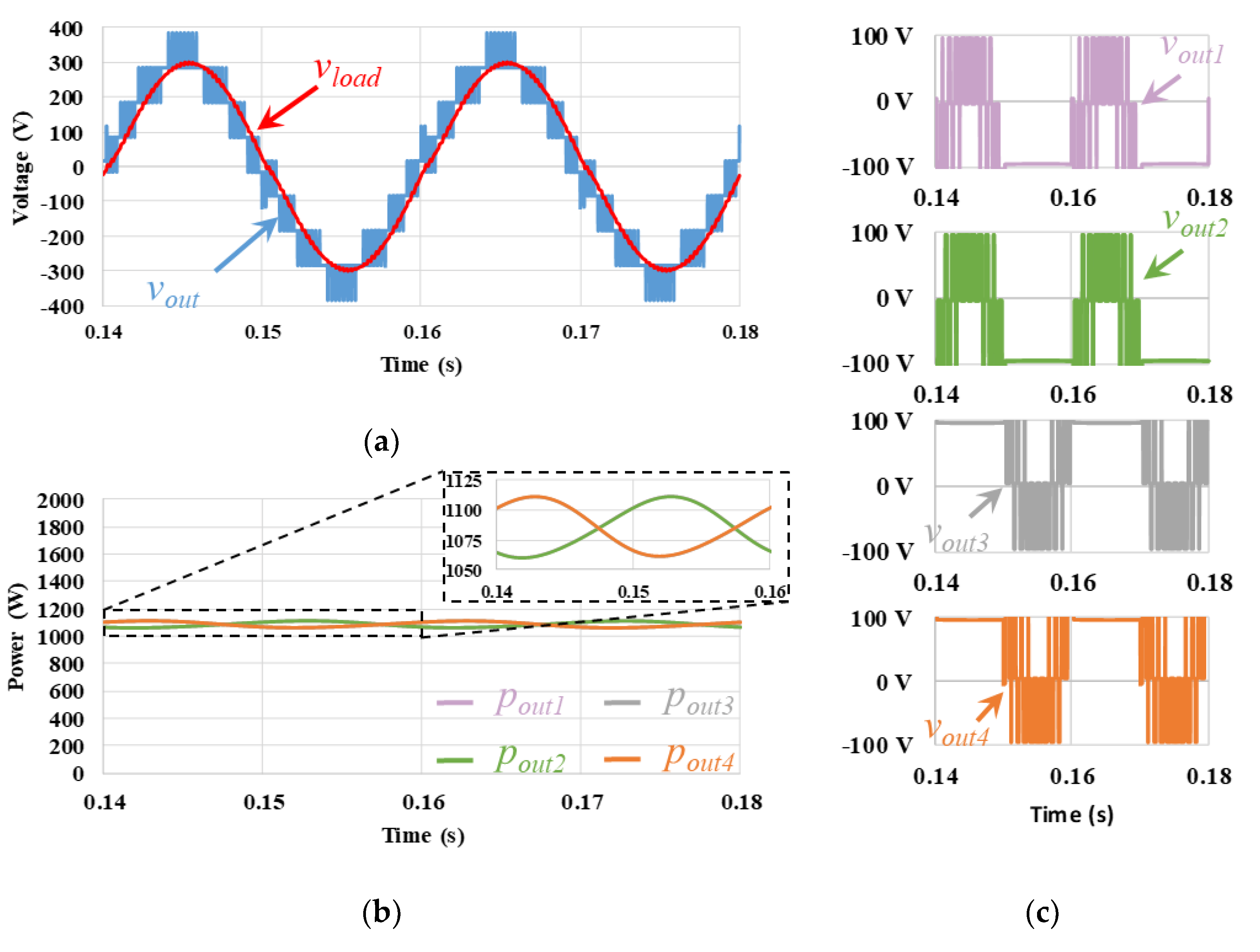
As far as the balancing techniques are concerned, the simulation results can be verified in the following figures: balanced PD in Figure 16, balanced POD in Figure 17, and balanced APOD in Figure 18. In analyzing the vout and vload waveforms, it is possible to verify that they present a greater symmetry resulting from the alternation of the carrier waves. In general, it was possible to minimize the power imbalances of each submodule. However, it should be mentioned that with the balanced PD technique (Figure 16b), each submodule presents a different average power value. In turn, with the balanced POD (Figure 17b) and balanced APOD (Figure 18b) techniques, the average power value is equal for each pair of modules. The alternation of carrier waves causes a higher number of intercepts to exist with the modulating wave for each submodule. As a result, the output voltages show a different pattern when compared to conventional unbalanced techniques: output voltages for balanced PD can be seen in Figure 16c; output voltages for balanced POD can be seen in Figure 17c; and output voltages for balanced APOD can be seen in Figure 18c.
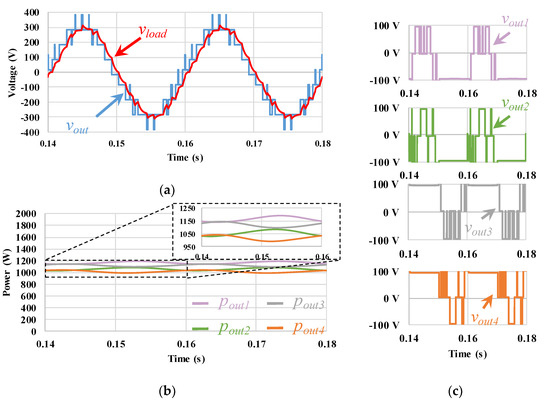
Figure 16.
Simulation results of the balanced PD PWM technique: (a) output voltage of the cascaded MLC, vout, and load voltage, vload; (b) output power on each submodule (pout1, pout2, pout3, pout4); (c) output voltage on each submodule (vout1, vout2, vout3, vout4).
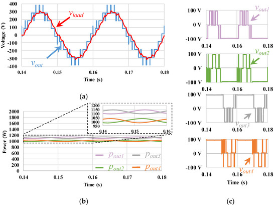
Figure 17.
Simulation results of the balanced POD PWM technique: (a) output voltage of the cascaded MLC, vout, and load voltage, vload; (b) output power on each submodule (pout1, pout2, pout3, pout4); (c) output voltage on each submodule (vout1, vout2, vout3, vout4).
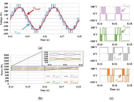
Figure 18.
Simulation results of the balanced APOD PWM technique: (a) output voltage of the cascaded MLC, vout, and load voltage, vload; (b) output power on each submodule (pout1, pout2, pout3, pout4); (c) output voltage on each submodule (vout1, vout2, vout3, vout4).
5.3. Level-Shift CO PWM Technique
The simulation results of the CO technique are shown in Figure 19. In Figure 19a are illustrated the waveforms of vout and vload. By analyzing the output waveforms, it can be seen that the positive half-cycle of vout is almost symmetrical to the negative half-cycle. Despite the non-symmetry of the carrier waves, the greater interception of the modulator waveform makes the switching frequency of the submodules higher, minimizing this symmetry difference. In Figure 19b are represented the power variations of each submodule. It should be mentioned that the submodules have an oscillating power of 50 Hz, with a 180° delay with the complementary submodule. That is, pout3 is 180° lagged in relation to pout2, and pout4 is 180° lagged in relation to pout1. It should also be mentioned that the pairs pout2 with pout3 and pout1 with pout4 present slightly different average power values due to the asymmetry of the carrier waveforms. Once again, it can be seen that the power distribution among the different submodules is not uniform, with some submodules contributing 2.1 times more power. Nevertheless, this is a lower value than that obtained with the PD, POD, and APOD PWM techniques. In Figure 19c, the output voltages (vout1, vout2, vout3, and vout4) of each submodule can be seen, verifying the difference in the patterns of each submodule. The areas of greater shading are the result of a higher switching of each submodule.
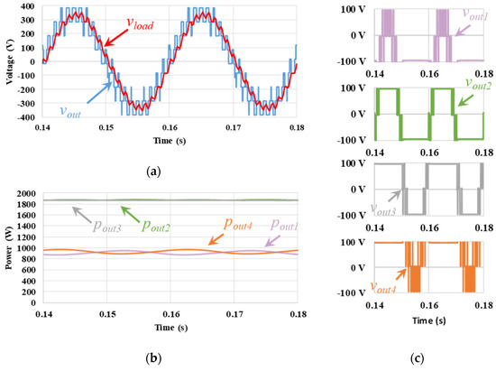
Figure 19.
Simulation results of the CO PWM technique: (a) output voltage of the cascaded MLC, vout, and load voltage, vload; (b) output power on each submodule (pout1, pout2, pout3, pout4); (c) output voltage on each submodule (vout1, vout2, vout3, vout4).
5.4. Level-Shift VF and VF2 PWM Techniques
Simulation results of the VF PWM technique are shown in Figure 20. By analyzing vout and vload represented in Figure 20a, it can be seen that the waveforms are not symmetrical about the zero-reference axis. Figure 20b shows the power variation of each submodule. It should be mentioned that the submodules have an oscillating power of 50 Hz, with a 180° delay with the complementary submodule. That is, pout3 is 180° lagged in relation to pout2, and pout4 is 180° lagged in relation to pout1. It should also be mentioned that the pairs pout2 with pout3 and pout1 with pout4 present slightly different average power values due to the asymmetry of the carrier waveforms. Once again, it can be seen that the power distribution is not uniform, with some submodules contributing 3.4 times more power. This fact is verified in Figure 20c, where each submodule shows a different pattern in the output voltage (vout1, vout2, vout3, and vout4). It is noteworthy that the higher and lower levels have higher switching frequencies, resulting from the increased frequency of the top- and lower-carrier waveforms.
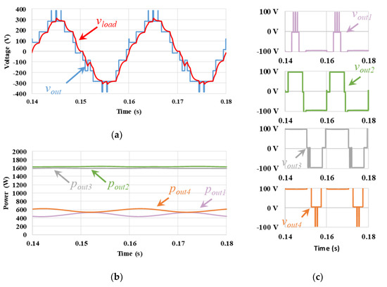
Figure 20.
Simulation results of the VF PWM technique: (a) output voltage of the cascaded MLC, vout, and load voltage, vload; (b) output power on each submodule (pout1, pout2, pout3, pout4); (c) output voltage on each submodule (vout1, vout2, vout3, vout4).
Figure 21 shows the simulation results of the other frequency variation technique, VF2. By analyzing the vout and vload represented in Figure 21, it can be seen that the waveforms are not symmetrical in relation to the zero-reference axis. Figure 21b shows the power variation of each submodule. It should be mentioned that the submodules have an oscillating power of 50 Hz, with a 180° delay with the complementary submodule. That is, pout3 is 180° lagged in relation to pout2, and pout4 is 180° lagged in relation to pout1. It should also be mentioned that the pairs pout2 with pout3 and pout1 with pout4 present slightly different average power values due to the asymmetry of the carrier waveforms. Once again, it can be seen that the power distribution is not uniform, with some submodules contributing 3.3 times more power. This fact is verified in Figure 21c, where each submodule shows a different pattern in the output voltage (vout1, vout2, vout3, and vout4). It should be noted that the intermediate voltage levels have higher switching frequencies, resulting from the increased frequency of the carrier wave.
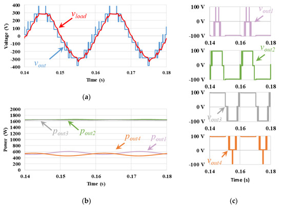
Figure 21.
Simulation results of the VF2 PWM technique: (a) output voltage of the cascaded MLC, vout, and load voltage, vload; (b) output power on each submodule (pout1, pout2, pout3, pout4); (c) output voltage on each submodule (vout1, vout2, vout3, vout4).
5.5. Phase-Shift Carrier PWM Technique
Figure 22 presents the simulation results for the PSC technique. Analyzing Figure 22a, it is possible to verify that the vout and vload waveforms present symmetry in relation to the zero-reference axis. It should be mentioned that the PSC technique allows for uniform power distribution over the different submodules, as can be seen by analyzing Figure 22b. The power of each submodule presents an oscillation of 50 Hz in phase and with similar average values in all submodules. The power contribution by the different modules is almost unitary (factor of 1.0006 between the submodule with the higher average power and the submodule with the lower average power). This fact is verified in Figure 22c, where each submodule presents a similar output voltage (vout1, vout2, vout3, and vout4) pattern among them. It should be mentioned that due to a greater intersection of the modulating waveforms with the carrier waves, vout has a greater number of commutations, causing the vload waveform to be practically sinusoidal, as illustrated in Figure 22c.

Figure 22.
Simulation results of the PSC PWM technique: (a) output voltage of the cascaded MLC, vout, and load voltage, vload; (b) output power on each submodule (pout1, pout2, pout3, pout4); (c) output voltage on each submodule (vout1, vout2, vout3, vout4).
5.6. Hybrid Carrier PSD PWM Technique
Figure 23 presents the simulation results regarding the PSD technique. By analyzing Figure 23a, it is possible to verify that the vout and vload waveforms present symmetry in relation to the zero-reference axis. It should be mentioned that the PSD technique allows uniform distribution of the average power value across the different submodules, as can be seen in Figure 23b. The power contribution by the different modules is almost unitary (factor of 1.0002 between the submodule with the higher average power and the submodule with the lower average power). The power of each submodule presents an oscillation of 50 Hz with a 180° delay. However, the complementary submodule is the adjacent one. That is, pout2 is 180° lagged in relation to pout1, and pout4 is 180° lagged in relation to pout3. This fact is seen in Figure 23c, where pairs of submodules (submodule 1 with submodule 2, submodule 3 with submodule 4) present a similar output voltage pattern between them (vout1, vout2, vout3, and vout4). It should be mentioned that due to a greater interception of the modulating waveforms with the carrier waveforms, vout has a greater number of commutations, causing the vload waveform to be practically sinusoidal.
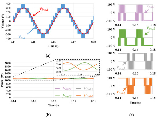
Figure 23.
Simulation results of the PSD PWM technique: (a) output voltage of the cascaded MLC, vout, and load voltage, vload; (b) output power on each submodule (pout1, pout2, pout3, pout4); (c) output voltage on each submodule (vout1, vout2, vout3, vout4).
5.7. Hybrid Carrier CO-PD, CO-POD, and CO-APOD PWM Techniques
Figure 24 presents the simulation results regarding the hybrid CO-PD technique. Analyzing Figure 24a, it is possible to verify that the vout and vload waveforms do not present symmetry in relation to the zero-reference axis, as had already happened with the PD PWM technique. In analyzing Figure 24b, it is possible to see that the CO-PD technique does not impose a uniform distribution of power over the different submodules. It should be mentioned that the submodules have an oscillating power of 50 Hz, with a 180° delay with the complementary submodule. That is, pout3 is 180° lagged in relation to pout2, and pout4 is 180° lagged in relation to pout1. It should also be mentioned that the pairs pout2 with pout3 and pout1 with pout4 present slightly different average power values due to the asymmetry of the carrier waveforms. Once again, it can be seen that the power distribution is not uniform, with some submodules contributing 2.2 times more power. This fact is verified in Figure 24c, where each submodule presents a different pattern in the output voltage (vout1, vout2, vout3, and vout4). It should be mentioned that despite a greater interception of the modulating waveform with the carrier waveforms, imposing vout to have a greater number of commutations, the vload does not present a more sinusoidal waveform than the PD technique.
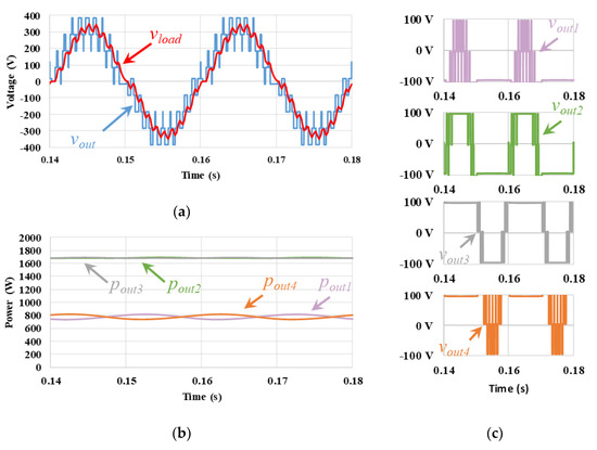
Figure 24.
Simulation results of the CO-PD PWM technique: (a) output voltage of the cascaded MLC, vout, and load voltage, vload; (b) output power on each submodule (pout1, pout2, pout3, pout4); (c) output voltage on each submodule (vout1, vout2, vout3, vout4).
Figure 25 presents the simulation results for the hybrid CO-POD technique. By analyzing Figure 25a, it is possible to verify that the vout and vload waveforms present symmetry with respect to the zero-reference axis, as happened with the POD technique. By analyzing Figure 25b, it is possible to see that the CO-POD technique does not impose a uniform distribution of power over the different submodules. It should be mentioned that the submodules have an oscillating power of 50 Hz with a 180° delay with the complementary submodule. That is, pout3 is 180° lagged in relation to pout2, and pout4 is 180° lagged in relation to pout1. It should also be mentioned that the pairs pout2 with pout3 and pout1 with pout4 present slightly different average power values, due to the asymmetry of the carrier waveforms. Once again, it can be seen that the power distribution is not uniform, with some submodules contributing 2.2 times more power. This fact is verified in Figure 25c, where each submodule presents a different output voltage pattern among them (vout1, vout2, vout3, and vout4). It should be mentioned that despite a greater interception of the modulating waveform with the carrier waveforms, imposing vout to have a greater number of voltage level variations, the vload does not present a more sinusoidal waveform than the POD technique. The modulation index and a current control algorithm should be adjusted and implemented, respectively.

Figure 25.
Simulation results of the CO-POD PWM technique: (a) output voltage of the cascaded MLC, vout, and load voltage, vload; (b) output power on each submodule (pout1, pout2, pout3, pout4); (c) output voltage on each submodule (vout1, vout2, vout3, vout4).
Figure 26 presents the simulation results for the hybrid CO-APOD technique. In analyzing Figure 26a, it is possible to verify that the vout and vload waveforms present symmetry with respect to the zero-reference axis, as happened with the APOD technique. In analyzing Figure 26b, it is possible to see that the CO-APOD technique does not impose a uniform distribution of power over the different submodules. It should be mentioned that the submodules have an oscillating power of 50 Hz with a 180° delay with the complementary submodule. That is, pout3 is 180° lagged in relation to pout2, and pout4 is 180° lagged in relation to pout1. It should also be mentioned that the pairs pout2 with pout3 and pout1 with pout4 present slightly different average power values, due to the asymmetry of the carrier waveforms. Once again, it can be seen that the power distribution is not uniform, with some submodules contributing 2.2 times more power. This fact is verified in Figure 26c, where each submodule presents a different output voltage pattern among them (vout1, vout2, vout3, and vout4). It should be mentioned that despite a greater intersection of the modulating waveform with the carrier waveforms, imposing vout to have a greater number of voltage level variations, the vload does not present a more sinusoidal waveform than the APOD technique. The modulation index and a current control algorithm should be adjusted and implemented, respectively.
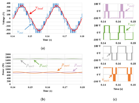
Figure 26.
Simulation results of the CO-APOD PWM technique: (a) output voltage of the cascaded MLC, vout, and load voltage, vload; (b) output power on each submodule (pout1, pout2, pout3, pout4); (c) output voltage on each submodule (vout1, vout2, vout3, vout4).
5.8. Comparative Analysis
Table 6 shows the output power and efficiency values of each submodule for the different PWM modulation techniques. In order to determine the power imbalance, the following methodologies were considered: (i) determine the high difference in modulus between the average output power of a given submodule k, Poutk, and the average value of the four submodules, Pavg; (ii) divide the maximum modulus value of this difference by the average output power of the four submodules, Pavg. The valor of Pavg is equal to Pout/4. By analyzing Table 6, it is possible to conclude that the level shift techniques create a greater power imbalance between the different submodules. In turn, the PSC and PSD techniques, due to the horizontal shift and a greater intersection of the modulator wave with the carrier, allow each submodule to contribute in a similar way, standardizing the operating power of each submodule. This feature is important for system modularity. The PSC and PSD PWM techniques were able to obtain an average value of the imbalance of power between the different submodules of 0.032% and 0.0117%, respectively. These PWM techniques have a substantially lower imbalance values compared to the other PWM techniques, such as the balanced POD, which follows with the lowest value of 5.01%. Regarding the techniques with overlapping waves, it can be seen that, for a fixed modulation index, each submodule contributes a higher power. As such, it is recommended that the modulation index be correctly sized according to the implemented PWM technique. On the other hand, it should be mentioned that the balancing PWM technique, used together with PD, POD, and APOD, allowed for the lowering of the power imbalance by 87.68% for the balanced PD PWM technique, by 90.16% for the POD PWM technique, and by 89.63% for the APOD PWM technique. Despite the strong impact on minimizing the power imbalance between submodules, these are still far from the values obtained with PSC and PSD.

Table 6.
Comparative output power and efficiency on each submodule and total power imbalance.
Regarding efficiency, it was determined as the ratio of the average value of the output power to the average value of the input power for each submodule. With that, it was possible to conclude that the PD, POD, and APOD techniques present the maximum efficiency values in a given submodule compared to the other techniques. However, due to the non-uniformity of the submodules, there are submodules with lower efficiencies, presenting average values for the total system of around 91.5%. The PSC and PSD PWM techniques present a uniform efficiency for each submodule, despite presenting a lower value compared to the maximums achieved with the other techniques. This uniform operation allowed for obtaining 93.5% efficiency in terms of average values of all submodules. This characteristic is justified by the greater number of interactions of the modulation waveform with the carrier waveforms, causing a greater number of output voltage levels variations steps.
Table 7 shows the total harmonic distortion as percentages of the fundamental (THD%f) values measured at the MMCC output, vout, and at the load terminals, vload, for different PWM techniques. In general, it can be concluded that the different PWM techniques presented similar results in vout. It should be mentioned that CO PWM techniques cause greater harmonic distortion. These characteristics are reflected in vload, presenting 2.56 % and 2.77 % as the lowest THD%f values in PSC and PSD techniques, respectively.

Table 7.
Comparative THD%f values of the MMCC output voltage, vout, and the load voltage, vload, for different PWM techniques.
In Figure 27 is represented the vout harmonic spectrum for different PWM techniques.
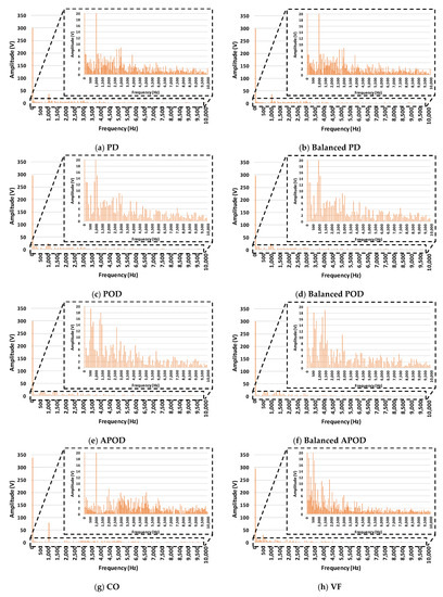
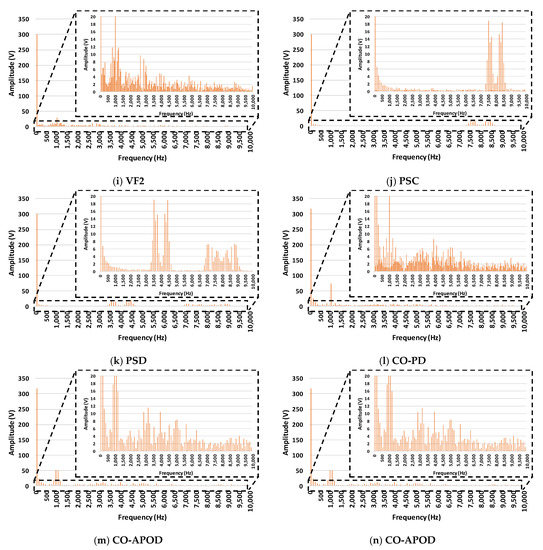
Figure 27.
Harmonic spectrum of the vout for different PWM techniques: (a) PD, (b) Balanced PD, (c) POD, (d) Balanced POD, (e) APOD, (f) Balanced APOD, (g) CO, (h) VF, (i) VF2, (j) PSC, (k) PSD, (l) CO-PD, (m) CO-POD, and (n) CO-APOD.
Regarding the PD (Figure 27a and balanced in Figure 27b), POD (Figure 27c and balanced in Figure 27d), and APOD (Figure 27e and balanced in Figure 27f) PWM techniques, it was possible to observe a lot of harmonic content. The harmonic spectrum originated by the PD technique has a higher density. It was possible to verify that the balancing techniques in these control techniques have little influence on the originated harmonic spectrum. The fundamental switching component is very evident in the existing spectrum. The value of 1 kHz also stands out for higher frequencies, although in the APO technique, the frequency of 1 kHz has a very low amplitude. Concerning the multiple frequency values of the switching frequency, this effect is not very evident.
Regarding the CO PWM technique (Figure 27g), it was possible to verify that the harmonic spectrum is much denser at higher frequencies than at low frequencies. In turn, with the VF (Figure 27h) and VF2 (Figure 27i) PWM techniques, the harmonic spectrum is denser at lower frequencies.
Regarding the PSC (Figure 27j) technique, it was possible to verify that it is the PWM technique whose harmonic spectrum at high frequencies is quite low. However, it should be noted that the harmonic content around the 8 kHz frequency is quite pronounced. The same is reflected with the PSD (Figure 27k) PWM technique, as the existing high-frequency harmonic content is quite focused on two points: (i) around 4 kHz (ii) around 8 kHz.
6. Discussion
In this topic, the main conclusions of the study are discussed. In focusing initially on modular and multilevel solutions, it can be seen that there is a strong interest in developing new solutions and improving actual solutions. The main challenge of these systems lies in the control algorithms capable of balancing the voltages of the different DC buses. The higher the number of levels, the higher the number of DC buses to be balanced and the higher the order of the problem to be solved. This control is required to be effective and dynamic and to minimize circulating currents.
From the developed study, it was verified that the SST has been showing a growing interest in the scientific community in the development of modular, multilevel solutions for high voltages and powers. In the SST group, it should be mentioned that the trend is that the submodules have a shared DC bus. This feature simplifies the DC bus control algorithms and, by having a DC bus with a lower common voltage, allows connection with other energy sources, such as renewable energies or energy storage systems. However, with the insertion of more submodules, more control signals are needed, as well as more signals to be acquired. All this management is limited to the peripherals that the centralized control system is able to provide. In order to mitigate this limitation, one of the trends in modular and multilevel systems is the decentralization of the control system. This means that each submodule will have a dedicated microcontroller that must follow orders from a master controller. The master is responsible for controlling the startup of the system and for determining the operating reference values. This information is transmitted to each slave microcontroller, who is responsible for controlling the power semiconductors and acquiring the operating values of the submodule. This new information would later be available to the master for processing. A fertile field of investigation is expected where it is necessary to determine the best communication approach in order to obtain an ideal ratio between propagation speeds and the number of peripherals/pins.
As far as PWM techniques are concerned, it can be seen that they cause different behaviors, requiring the correct choice and configuration depending on the application. Taking into account the topology with cascade full-bridges, it was possible to conclude that in case the carrier waves have symmetry in relation to the zero-reference axis, the output waves of the power electronics converter also have symmetry, which can facilitate the control system gain adjustment. However, the different arrangements of the carrier waves give rise to different output voltages in each submodule. Consequently, there may be submodules with very different operating powers compared to the underlying modules. Thus, the need for a careful study at the level of different control techniques in order to maintain the modularity of the system becomes evident. PWM techniques for the balancing of power between submodules were presented and quantified, concluding that these can minimize the imbalances. It should be mentioned that the power values of each submodule can have different mean values, phase angles, and oscillation patterns, which can reduce the performance of the DC bus regulation algorithms. Of the results obtained, it is worth mentioning the PSC technique, whose power of each submodule is similar and coincident over the time. It was also possible to verify that, due to the superposition of the carrier waves of some PWM techniques, it is possible to obtain a higher output power, with the same modulation index, when compared to other techniques. The need for the correct sizing of the modulation index in order to obtain a correct system performance becomes evident.
In order to compare the different PWM techniques in terms of quality of the load waveform, the THD%f was calculated, and it was observed that the THD%f varies from 2.56% for the PSC or 2.77% for the PSD to 11.1% for the CO-PD or 10.7% for the CO-POD techniques. These are ideal values; in particular, they do not take into account the dead-time or the DC bus voltage ripple influence. However, the conditions are the same for all methods.
As far as THD%f values are concerned, it was possible to quantify the different PWM techniques, concluding that the PSC and PSD techniques presented the lowest THD%f values.
Regarding the harmonic spectrum, it was possible to verify that there are techniques that give rise to an accentuated harmonic dispersion, which makes difficult the design of passive filters. However, the performance of the PSC technique, whose harmonic spectrum is concentrated in the frequency of 8 kHz, should be highlighted. This frequency can be justified as being a multiple of the switching frequency. That is, considering that there are four submodules connected in series, where each submodule is operating with a unipolar 1 kHz switching frequency, the resulting frequency is 8 kHz. This feature is interesting in modular and multilevel systems in order to multiply the operating frequencies, and thus it is possible to minimize the output passive filters.
7. Conclusions
This work presents a comparative study of different topologies of multilevel converters (MLC) capable of expanding or presenting modularity, as well as a comparative study of different pulse width modulation (PWM) techniques when applied to MLC.
The evolution of the MLC concept is presented, highlighting the future challenges in the concept of modularity and multilevel converters. The characteristics and advantages of this concept are presented. Regarding the topologies, the topologies of half-bridge with split DC bus, the submodule of the half-bridge of the complete DC bus, the full-bridge, the neutral-point clamped (NPC) converter, the NPC as the submodule, the T-type NPC topology, the flying capacitor multilevel converter (FCMC), and the FCMC submodule concept were presented. Different applications for each topology were presented, not only in their expandability in order to increase the number of output levels, but also their modularity when used in the modular multilevel converter (MMC) or cascaded MMC (MMCC) concepts. A comparative table of different topologies at the implementation level is presented. Tables relating to applications for different topologies, as well as analysis of electrical operating parameters of different solutions on the market and experimental prototypes are presented.
In this analysis, it was possible to verify that the full-bridge topology presents a widely versatile solution for different applications, presenting a simple hardware with a widely known implementation complexity. NPC topology is widely used in high-power but low-voltage applications. In turn, the MMC composed of the half-bridge submodule topology is more used in applications with high voltages. Note that the greater the number of output voltage and power levels, the lower the switching frequencies can be. The solid-state transformer (SST) concept is also presented, analyzing different MLC topologies to be integrated.
Considering the investment of an MLC and its complexity, its continuous operation is required. For this, failure detection, failure protection, and failure recovery mechanisms are necessary. Different solutions were presented, distinguishing the redundancy methods in hot reserve and cold reserve.
As far as PWM techniques are concerned, based on computational simulations employed in the MMCC topology with complete bridges, it was possible to analyze different performances. The vertical displacement of the carrier waves presents interesting performance characteristics, and depending on the technique implemented, the synthesized output wave may or may not have symmetry but always maintains an imbalance of power between submodules. In order to mitigate this problem, alternation techniques were proposed and analyzed, verifying the balance of operating powers of each submodule. The horizontal displacement technique, in addition to a greater simplicity of implementation, taking into account the existing microcontrollers, allows not only a greater balance of power between different submodules, but also a greater number of intercepts between modulating and carrier waves. As such, the output waveform has a higher number of variations, increasing the output ripple frequency. In turn, with the overlapping techniques, the submodules will contribute a higher power for the same modulation index value. As such, it is recommended as the correct choice of the modulation technique, as well as the modulation index, depending on the adopted topology. It should also be mentioned that there are techniques more suited to some topologies than others, namely the variable frequency approach for cascade solutions and another variable frequency approach for NPC.
In quantitative terms, it was possible to conclude that the PSC, PSD, and CO-PD PWM techniques presented an average power value of each submodule of 93.5%. Due to the horizontal arrangement, the PSC and PSD techniques presented a maximum imbalance value between submodules of 0.032% and 0.011%, respectively. The standardization of power operations for each submodule that constitutes a modular and multilevel solution is an important requirement. Additionally, in terms of total harmonic distortion as a percentage of the fundamental (THD%f), it was possible to quantify a minimum value of 2.56% and 2.77% for the PSC and PSD techniques, respectively. These THD%f values represent a value of more than half when compared to the lowest THD%f value of the other PWM techniques analyzed.
In short, with the development of power electronics for applications in renewable energy production plants, electric mobility applications, railway electrical systems, and smart grids, among others, the MLC concept plays an important role in better functionality. Thus, the development of new concepts, as well as concept improvements, is important, and this paper is intended to provide a starting point for analysis and practical implementation for MLC.
In terms of practical implementation, a detailed study of the system to be implemented is necessary, analyzing the advantages and disadvantages of each power electronics topology together with the PWM techniques. Regarding the power hardware, analysis of the topology is recommended, as well as the configuration of the modular and multilevel converter that best meets the requirements of the system to be implemented. As a solution of several power submodules connected in cascade, consequently several semiconductors in series, the integration of power semiconductor modules with low forward voltage drop, as well as low internal resistance, is recommended in order to maximize the efficiency of the system. The smaller the forward voltage drop of the semiconductors, the closer the DC bus voltage can be to the output voltage. On the other hand, the junction of different square waves at the output of each submodule makes it possible to obtain output frequencies that are multiples of the frequencies of the carrier waves. In this way, it is possible to integrate a more compact passive filter.
As far as the implementation is concerned, it is necessary to study the PWM peripherals that constitute the digital control platforms, with the modulating and carrier waves being adjusted to their amplitude. Conventional microcontrollers have dedicated registers for the horizontal shift of the carrier waves. However, in PWM techniques with vertical displacement, the implementation becomes more complex. In this case, the modulating waveform must be adjusted, considering the amplitude of the carrier waves in order to obtain the comparison points and, thus, the desired switching profile. FPGA emerges as a platform with the versatility to implement the vertical displacement of carrier waves, thus not requiring the constant reconfiguration of the modulating waveform. However, with the need to add more submodules, the peripherals must be readjusted. In this way, it is expected that the decentralization of the control system can be an assiduous presence in modular and multilevel systems in order to boost the concept of modularity. In a decentralized system, it is possible to identify a master responsible for managing the different slaves. In turn, each slave is responsible for acquiring signals and controlling the PWM signals of each submodule. With the need to increase the number of interface levels of the solution, it is only necessary to add more dedicated submodules. However, this solution presents as a major challenge the time management of the processing of the control algorithms and the communication between different submodules, being a very fertile field of investigation in the area of MMC.
In a system with different submodules, it is possible to predict the existence of slightly different impedances and components. These differences between submodules lead to imbalances. Therefore, PWM techniques must be combined with voltage-balancing control algorithms for each submodule.
In future work, we intend to proceed with the comparative study by means of experimental results. For this, it would be necessary to develop a laboratory prototype where the different PWM modulation techniques would be implemented in a microcontroller. This study could help in the configuration of carrier and modulating waveforms for each PWM technique in a microcontroller, making the configuration available for those who want to study and implement MMC.
Author Contributions
Conceptualization, L.A.M.B.; investigation, L.A.M.B.; methodology, L.A.M.B.; software, L.A.M.B.; supervision, A.P.M. and J.G.P.; writing—original draft, L.A.M.B.; writing—review & editing, L.A.M.B., A.P.M., and J.G.P. All authors have read and agreed to the published version of the manuscript.
Funding
This work has been supported by FCT—Fundação para a Ciência e Tecnologia, within the R&D Units Project Scope UIDB/00319/2020. Mr. Luis A. M. Barros is supported by the doctoral scholarship PD/BD/143006/2018, granted by the Portuguese FCT foundation.
Institutional Review Board Statement
Not applicable.
Informed Consent Statement
Not applicable.
Data Availability Statement
Due to confidentiality restrictions, no data is made publicly available from this study.
Conflicts of Interest
The authors declare no conflict of interest.
References
- Vijeh, M.; Rezanejad, M.; Samadaei, E.; Bertilsson, K. A general review of multilevel inverters based on main submodules: Structural point of view. IEEE Trans. Power Electron. 2019, 34, 9479–9502. [Google Scholar] [CrossRef]
- Barros, L.A.; Tanta, M.; Martins, A.P.; Afonso, J.L.; Pinto, J.G. Submodule Topologies and PWM Techniques Applied in Modular Multilevel Converters: Review and Analysis. In Proceedings of the International Conference on Sustainable Energy for Smart Cities, Viana do Castelo, Portugal, 3 December 2020; pp. 111–131. [Google Scholar]
- Gupta, K.K.; Bhatnagar, P. Multilevel Inverters: Conventional and Emerging Topologies and Their Control; Hayton, J., Ed.; Elsevier: Amsterdam, The Netherlands; Academic Press: Cambridge, MA, USA, 2017. [Google Scholar]
- Rashid, M.H. Power Electronics Handbook, 4th ed.; Elsevier: Amsterdam, The Netherlands; Butterworth-Heinemann: Oxford, UK, 2017. [Google Scholar]
- Sharifabadi, K.; Harnefors, L.; Nee, H.-P.; Norrga, S.; Teodorescu, R. Design, Control, and Application of Modular Multilevel Converters for HVDC Transmission Systems; IEEE Press: Piscataway, NJ, USA; John Wiley & Sons: Hoboken, NJ, USA, 2016. [Google Scholar]
- Feldman, R.; Tomasini, M.; Amankwah, E.; Clare, J.C.; Wheeler, P.W.; Trainer, D.R.; Whitehouse, R.S. A hybrid modular multilevel voltage source converter for HVDC power transmission. IEEE Trans. Ind. Appl. 2013, 49, 1577–1588. [Google Scholar] [CrossRef]
- Jung, J.-J.; Cui, S.; Lee, J.-H.; Sul, S.-K. A new topology of multilevel VSC converter for a hybrid HVDC transmission system. IEEE Trans. Power Electron. 2016, 32, 4199–4209. [Google Scholar] [CrossRef]
- Du, S.; Dekka, A.; Wu, B.; Zargari, N. Modular Multilevel Converters: Analysis, Control, and Applications; John Wiley & Sons: Hoboken, NJ, USA, 2017. [Google Scholar]
- Engel, S.P.; Stieneker, M.; Soltau, N.; Rabiee, S.; Stagge, H.; De Doncker, R.W. Comparison of the modular multilevel DC converter and the dual-active bridge converter for power conversion in HVDC and MVDC grids. IEEE Trans Power Electron. 2014, 30, 124–137. [Google Scholar] [CrossRef]
- Huang, S. Distributed Modulation and Control of Modular Multilevel Converter for HVDC Application. Master’s Thesis, Aalborg University, Aalborg, Denmark, 2013. [Google Scholar]
- Song, G.; Wang, T.; Huang, X.; Zhang, C. An improved averaged value model of MMC-HVDC for power system faults simulation. Int. J. Electr. Power Energy Syst. 2019, 110, 223–231. [Google Scholar] [CrossRef]
- Li, X.; Song, Q.; Liu, W.; Rao, H.; Xu, S.; Li, L. Protection of nonpermanent faults on DC overhead lines in MMC-based HVDC systems. IEEE Trans. Power Deliv. 2012, 28, 483–490. [Google Scholar] [CrossRef]
- Son, G.T.; Lee, H.-J.; Nam, T.S.; Chung, Y.-H.; Lee, U.-H.; Baek, S.-T.; Hur, K.; Park, J.-W. Design and control of a modular multilevel HVDC converter with redundant power modules for noninterruptible energy transfer. IEEE Trans. Power Deliv. 2012, 27, 1611–1619. [Google Scholar]
- Ferreira, A.A. de A. Modular multilevel converters for power system applications. Ph.D. Thesis, Universitat Politècnica de Catalunya, Barcelona, Spain, 2017. [Google Scholar]
- Zhou, L.; Fu, Q.; Li, X.; Liu, C. A novel photovoltaic grid-connected power conditioner employing hybrid multilevel inverter. In Proceedings of the 2009 International Conference on Sustainable Power Generation and Supply, Nanjing, China, 6–7 April 2009; pp. 1–7. [Google Scholar]
- Latran, M.B.; Teke, A. Investigation of multilevel multifunctional grid connected inverter topologies and control strategies used in photovoltaic systems. Renew. Sustain. Energy Rev. 2015, 42, 361–376. [Google Scholar] [CrossRef]
- Lashab, A.; Sera, D.; Hahn, F.; Camurca, L.; Terriche, Y.; Liserre, M.; Guerrero, J.M. Cascaded multilevel PV inverter with improved harmonic performance during power imbalance between power cells. IEEE Trans. Ind. Appl. 2020, 56, 2788–2798. [Google Scholar] [CrossRef]
- Basu, T.S.; Maiti, S. A hybrid modular multilevel converter for solar power integration. IEEE Trans. Ind. Appl. 2019, 55, 5166–5177. [Google Scholar] [CrossRef]
- Acharya, A.B.; Ricco, M.; Sera, D.; Teoderscu, R.; Norum, L.E. Performance analysis of medium-voltage grid integration of PV plant using modular multilevel converter. IEEE Trans. Energy Convers. 2019, 34, 1731–1740. [Google Scholar] [CrossRef]
- Rojas, C.A.; Kouro, S.; Perez, M.A.; Echeverria, J. DC-DC MMC for HVdc grid interface of utility-scale photovoltaic conversion systems. IEEE Trans. Ind. Electron. 2017, 65, 352–362. [Google Scholar] [CrossRef]
- Nademi, H.; Das, A.; Burgos, R.; Norum, L.E. A new circuit performance of modular multilevel inverter suitable for photovoltaic conversion plants. IEEE J. Emerg. Sel. Top. Power Electron. 2015, 4, 393–404. [Google Scholar] [CrossRef]
- Rong, F.; Gong, X.; Huang, S. A novel grid-connected PV system based on MMC to get the maximum power under partial shading conditions. IEEE Trans. Power Electron. 2016, 32, 4320–4333. [Google Scholar] [CrossRef]
- Debnath, S.; Saeedifard, M. A new hybrid modular multilevel converter for grid connection of large wind turbines. IEEE Trans. Sustain. Energy 2013, 4, 1051–1064. [Google Scholar] [CrossRef]
- Li, R.; Yu, L.; Xu, L.; Adam, G.P. Coordinated control of parallel DR-HVDC and MMC-HVDC systems for offshore wind energy transmission. IEEE J. Emerg. Sel. Top. Power Electron. 2019, 8, 2572–2582. [Google Scholar] [CrossRef]
- Karaagac, U.; Mahseredjian, J.; Cai, L.; Saad, H. Offshore wind farm modeling accuracy and efficiency in MMC-based multiterminal HVDC connection. IEEE Trans. Power Deliv. 2016, 32, 617–627. [Google Scholar] [CrossRef]
- Vidal-Albalate, R.; Beltran, H.; Rolán, A.; Belenguer, E.; Peña, R.; Blasco-Gimenez, R. Analysis of the performance of MMC under fault conditions in HVDC-based offshore wind farms. IEEE Trans. Power Deliv. 2015, 31, 839–847. [Google Scholar] [CrossRef] [Green Version]
- Islam, M.R.; Guo, Y.; Zhu, J. A high-frequency link multilevel cascaded medium-voltage converter for direct grid integration of renewable energy systems. IEEE Trans. Power Electron. 2013, 29, 4167–4182. [Google Scholar] [CrossRef]
- Kwon, K.; Choi, J. Single-Phase 13-Level Power Conditioning System for Peak Power Reduction of a High-Speed Railway Substation. Energies 2019, 12, 4405. [Google Scholar] [CrossRef] [Green Version]
- Bayat, H.; Yazdani, A. A hybrid MMC-based photovoltaic and battery energy storage system. IEEE Power Energy Technol. Syst. J. 2019, 6, 32–40. [Google Scholar] [CrossRef]
- Amin, M.; Rygg, A.; Molinas, M. Self-synchronization of wind farm in an MMC-based HVDC system: A stability investigation. IEEE Trans. Energy Convers. 2017, 32, 458–470. [Google Scholar] [CrossRef]
- Zhang, L.; Tang, Y.; Yang, S.; Gao, F. Decoupled power control for a modular-multilevel-converter-based hybrid AC-DC grid integrated with hybrid energy storage. IEEE Trans. Ind. Electron. 2018, 66, 2926–2934. [Google Scholar] [CrossRef]
- Maharjan, L.; Yamagishi, T.; Akagi, H.; Asakura, J. Fault-tolerant operation of a battery-energy-storage system based on a multilevel cascade PWM converter with star configuration. IEEE Trans. Power Electron. 2010, 25, 2386–2396. [Google Scholar] [CrossRef]
- Maharjan, L.; Yamagishi, T.; Akagi, H. Active-power control of individual converter cells for a battery energy storage system based on a multilevel cascade PWM converter. IEEE Trans. Power Electron. 2010, 27, 1099–1107. [Google Scholar] [CrossRef]
- Zhou, Y.; Jiang, D.; Guo, J.; Hu, P.; Liang, Y. Analysis and control of modular multilevel converters under unbalanced conditions. IEEE Trans. Power Deliv. 2013, 28, 1986–1995. [Google Scholar] [CrossRef]
- Soong, T.; Lehn, P.W. Assessment of fault tolerance in modular multilevel converters with integrated energy storage. IEEE Trans. Power Electron. 2015, 31, 4085–4095. [Google Scholar] [CrossRef]
- Weiss, D.; Vasiladiotis, M.; Banceanu, C.; Drack, N.; Odegard, B.; Grondona, A. IGCT based modular multilevel converter for an AC-AC rail power supply. In Proceedings of the PCIM Europe 2017: International Exhibition and Conference for Power Electronics, Intelligent Motion, Renewable Energy and Energy Management, Nuremberg, Germany, 16–18 May 2017; pp. 1–8. [Google Scholar]
- ElGebaly, A.E.; Hassan, A.E.-W.; El-Nemr, M.K. Reactive Power Compensation by Multilevel Inverter STATCOM for Railways Power Grid. In Proceedings of the 2019 IEEE Conference of Russian Young Researchers in Electrical and Electronic Engineering (EIConRus), Saint Petersburg, Moscow, 28–31 January 2019; pp. 2094–2099. [Google Scholar]
- Tanta, M.; Cunha, J.; Barros, L.A.; Monteiro, V.; Pinto, J.; Martins, A.P.; Afonso, J.L. Experimental Validation of a Reduced-Scale Rail Power Conditioner Based on Modular Multilevel Converter for AC Railway Power Grids. Energies 2021, 14, 484. [Google Scholar] [CrossRef]
- Dixon, J.; Pereda, J.; Castillo, C.; Bosch, S. Asymmetrical multilevel inverter for traction drives using only one DC supply. IEEE Trans. Veh. Technol. 2010, 59, 3736–3743. [Google Scholar] [CrossRef]
- Fazel, S.S.; Bernet, S.; Krug, D.; Jalili, K. Design and comparison of 4-kV neutral-point-clamped, flying-capacitor, and series-connected H-bridge multilevel converters. IEEE Trans. Ind. Appl. 2007, 43, 1032–1040. [Google Scholar] [CrossRef]
- Gan, C.; Sun, Q.; Wu, J.; Kong, W.; Shi, C.; Hu, Y. MMC-based SRM drives with decentralized battery energy storage system for hybrid electric vehicles. IEEE Trans. Power Electron. 2018, 34, 2608–2621. [Google Scholar] [CrossRef]
- Zheng, Z.; Wang, K.; Xu, L.; Li, Y. A hybrid cascaded multilevel converter for battery energy management applied in electric vehicles. IEEE Trans. Power Electron. 2013, 29, 3537–3546. [Google Scholar] [CrossRef]
- Ronanki, D.; Williamson, S.S. A simplified space vector pulse width modulation implementation in modular multilevel converters for electric ship propulsion systems. IEEE Trans. Transp. Electrif. 2018, 5, 335–342. [Google Scholar] [CrossRef]
- Chen, Y.; Li, Z.; Zhao, S.; Wei, X.; Kang, Y. Design and implementation of a modular multilevel converter with hierarchical redundancy ability for electric ship MVDC system. IEEE J. Emerg. Sel. Top. Power Electron. 2016, 5, 189–202. [Google Scholar] [CrossRef]
- Bina, M.T. A transformerless medium-voltage STATCOM topology based on extended modular multilevel converters. IEEE Trans. Power Electron. 2011, 26, 1534–1545. [Google Scholar]
- Cheng, Y.; Qian, C.; Crow, M.L.; Pekarek, S.; Atcitty, S. A comparison of diode-clamped and cascaded multilevel converters for a STATCOM with energy storage. IEEE Trans. Ind. Electron. 2006, 53, 1512–1521. [Google Scholar] [CrossRef]
- Merlin, M.M.; Green, T.C.; Mitcheson, P.D.; Trainer, D.R.; Critchley, R.; Crookes, W.; Hassan, F. The alternate arm converter: A new hybrid multilevel converter with dc-fault blocking capability. IEEE Trans. Power Deliv. 2013, 29, 310–317. [Google Scholar] [CrossRef] [Green Version]
- Song, W.; Huang, A.Q. Fault-tolerant design and control strategy for cascaded H-bridge multilevel converter-based STATCOM. IEEE Trans. Ind. Electron. 2009, 57, 2700–2708. [Google Scholar] [CrossRef]
- Akagi, H.; Inoue, S.; Yoshii, T. Control and performance of a transformerless cascade PWM STATCOM with star configuration. IEEE Trans. Ind. Appl. 2007, 43, 1041–1049. [Google Scholar] [CrossRef]
- Cupertino, A.F.; Farias, J.V.M.; Pereira, H.A.; Seleme, S.I.; Teodorescu, R. Comparison of DSCC and SDBC modular multilevel converters for STATCOM application during negative sequence compensation. IEEE Trans. Ind. Electron. 2018, 66, 2302–2312. [Google Scholar] [CrossRef]
- Gupta, R.; Ghosh, A.; Joshi, A. Control of cascaded transformer multilevel inverter based DSTATCOM. Electr. Power Syst. Res. 2007, 77, 989–999. [Google Scholar] [CrossRef]
- Liu, T.; Yang, X.; Chen, W.; Xuan, Y.; Li, Y.; Huang, L.; Hao, X. High-efficiency control strategy for 10-kV/1-MW solid-state transformer in PV application. IEEE Trans. Power Electron. 2020, 35, 11770–11782. [Google Scholar] [CrossRef]
- Liu, T.; Yang, X.; Chen, W.; Li, Y.; Xuan, Y.; Huang, L.; Hao, X. Design and implementation of high efficiency control scheme of dual active bridge based 10 kV/1 MW solid state transformer for PV application. IEEE Trans. Power Electron. 2018, 34, 4223–4238. [Google Scholar] [CrossRef]
- Parreiras, T.M.; Machado, A.P.; Amaral, F.V.; Lobato, G.C.; Brito, J.A.; Cardoso Filho, B. Forward dual-active-bridge solid-state transformer for a SiC-based cascaded multilevel converter cell in solar applications. IEEE Trans. Ind. Appl. 2018, 54, 6353–6363. [Google Scholar] [CrossRef]
- Liu, C.; Liu, C.; Cai, G.; Ying, H.; Zhang, Z.; Shan, R.; Pei, Z.; Song, X. An isolated modular multilevel converter (IM 2 C) topology based on high-frequency link (HFL) concept. IEEE Trans. Power Electron. 2019, 35, 1576–1588. [Google Scholar] [CrossRef]
- Madhusoodhanan, S.; Tripathi, A.; Patel, D.; Mainali, K.; Kadavelugu, A.; Hazra, S.; Bhattacharya, S.; Hatua, K. Solid-state transformer and MV grid tie applications enabled by 15 kV SiC IGBTs and 10 kV SiC MOSFETs based multilevel converters. IEEE Trans. Ind. Appl. 2015, 51, 3343–3360. [Google Scholar] [CrossRef]
- Kouro, S.; Malinowski, M.; Gopakumar, K.; Pou, J.; Franquelo, L.G.; Wu, B.; Rodriguez, J.; Pérez, M.A.; Leon, J.I. Recent advances and industrial applications of multilevel converters. IEEE Trans. Ind. Electron. 2010, 57, 2553–2580. [Google Scholar] [CrossRef]
- Akagi, H. Classification, terminology, and application of the modular multilevel cascade converter (MMCC). IEEE Trans. Power Electron. 2011, 26, 3119–3130. [Google Scholar] [CrossRef]
- Dekka, A.; Wu, B.; Fuentes, R.L.; Perez, M.; Zargari, N.R. Evolution of topologies, modeling, control schemes, and applications of modular multilevel converters. IEEE J. Emerg. Sel. Top. Power Electron. 2017, 5, 1631–1656. [Google Scholar] [CrossRef]
- Zhang, J.; Xu, S.; Din, Z.; Hu, X. Hybrid multilevel converters: Topologies, evolutions and verifications. Energies 2019, 12, 615. [Google Scholar] [CrossRef] [Green Version]
- Feng, J.; Chu, W.; Zhang, Z.; Zhu, Z. Power electronic transformer-based railway traction systems: Challenges and opportunities. IEEE J. Emerg. Sel. Top. Power Electron. 2017, 5, 1237–1253. [Google Scholar] [CrossRef]
- Nami, A.; Liang, J.; Dijkhuizen, F.; Demetriades, G.D. Modular multilevel converters for HVDC applications: Review on converter cells and functionalities. IEEE Trans. Power Electron. 2015, 30, 18–36. [Google Scholar] [CrossRef]
- Perez, M.A.; Bernet, S.; Rodriguez, J.; Kouro, S.; Lizana, R. Circuit topologies, modeling, control schemes, and applications of modular multilevel converters. IEEE Trans. Power Electron. 2014, 30, 4–17. [Google Scholar] [CrossRef]
- Deng, F.; Lü, Y.; Liu, C.; Heng, Q.; Yu, Q.; Zhao, J. Overview on submodule topologies, modeling, modulation, control schemes, fault diagnosis, and tolerant control strategies of modular multilevel converters. Chin. J. Electr. Eng. 2020, 6, 1–21. [Google Scholar] [CrossRef]
- Antonio-Ferreira, A.; Collados-Rodriguez, C.; Gomis-Bellmunt, O. Modulation techniques applied to medium voltage modular multilevel converters for renewable energy integration: A review. Electr. Power Syst. Res. 2018, 155, 21–39. [Google Scholar] [CrossRef] [Green Version]
- Debnath, S.; Qin, J.; Bahrani, B.; Saeedifard, M.; Barbosa, P. Operation, control, and applications of the modular multilevel converter: A review. IEEE Trans. Power Electron. 2014, 30, 37–53. [Google Scholar] [CrossRef]
- Mcmurray, W. Fast Response Stepped-Wave Switching Power Converter Circuit. U.S. Patent 3581212, 25 May 1971. [Google Scholar]
- Huber, J.E.; Kolar, J.W. Solid-state transformers: On the origins and evolution of key concepts. IEEE Ind. Electron. Mag. 2016, 10, 19–28. [Google Scholar] [CrossRef]
- Rego, J.; Pereira, F.L.; Barros, L.A.M.; Martins, A.P.; Pinto, J.G. Development of a Modular Multilevel Cascade Converter based on Full-Bridge Submodules with a common DC-Bus. In Proceedings of the EAI SESC 2021—3rd EAI International Conference on Sustainable Energy for Smart Cities, Online Conference, 24–26 November 2021. [Google Scholar]
- Baker, R.H. Bridge Converter Circuit. U.S. Patent 4 270 163, 26 May 1991. [Google Scholar]
- Nabae, A.; Takahashi, I.; Akagi, H. A new neutral-point-clamped PWM inverter. IEEE Trans. Ind. Appl. 1981, 5, 518–523. [Google Scholar] [CrossRef]
- Meynard, T.; Foch, H. Multi-level conversion: High voltage choppers and voltage-source inverters. In Proceedings of the PESC’92 Record. 23rd Annual IEEE Power Electronics Specialists Conference, Toledo, Spain, 29 June–3 July 1992; pp. 397–403. [Google Scholar]
- Rashid, M.H. Power Electronics Handbook: Devices, Circuits, and Applications, 3rd ed.; Elsevier: Amsterdam, The Netherlands; Butterworth-Heinemann: Oxford, UK, 2017. [Google Scholar]
- Maswood, A.I.; Tafti, H.D. Advanced Multilevel Converters and Applications in Grid Integration; John Wiley & Sons: Hoboken, NJ, USA, 2018. [Google Scholar]
- Brenna, M.; Foiadelli, F.; Zaninelli, D. Electrical Railway Transportation Systems; IEEE Press: Piscataway, NJ, USA; John Wiley & Sons: Hoboken, NJ, USA, 2018; Volume 67. [Google Scholar]
- Barros, L.A.M.; Tanta, M.; Martins, A.P.; Afonso, J.L.; Pinto, J.G. Opportunities and Challenges of Power Electronics Systems in Future Railway Electrification. In Proceedings of the IEEE CPE—POWERENG 2020: 14th International Conference on Compatibility, Power Electronics and Power Engineering, Setubal, Portugal, 8–10 July 2020. [Google Scholar]
- Kabalci, E. Multilevel Inverters: Control Methods and Advanced Power Electronic Applications; Elsevier: Amsterdam, The Netherlands; Academic Press: Cambridge, MA, USA, 2017. [Google Scholar]
- Talon Louokdom, E.; Gavin, S.; Siemaszko, D.; Biya-Motto, F.; Essimbi Zobo, B.; Marchesoni, M.; Carpita, M. Small-Scale Modular Multilevel Converter for Multi-Terminal DC Networks Applications: System Control Validation. Energies 2018, 11, 1690. [Google Scholar] [CrossRef] [Green Version]
- Talon, E.; Gavin, S.; Siemaszko, D.; Biya-Motto, F.; Essimbi, B.; Carpita, M. Design and implementation of a multi-dsp based digital control system architecture for modular multilevel converters. In Proceedings of the 2016 IEEE International Power Electronics and Motion Control Conference (PEMC), Varna, Bulgaria, 25–28 September 2016; pp. 1182–1187. [Google Scholar]
- Toh, C.L.; Norum, L. A high speed control network synchronization jitter evaluation for embedded monitoring and control in modular multilevel converter. In Proceedings of the 2013 IEEE Grenoble Conference, Grenoble, France, 16–20 June 2013; pp. 1–6. [Google Scholar]
- Fey, J.-H.; Hinrichsen, F.; Carstens, G.; Mallwitz, R. Development of a modular multilevel converter demonstrator with EtherCAT communication. In Proceedings of the 2019 IEEE 13th International Conference on Compatibility, Power Electronics and Power Engineering (CPE-POWERENG), Sonderborg, Denmark, 23–25 April 2019; pp. 1–6. [Google Scholar]
- Rietmann, S.; Fuchs, S.; Hillers, A.; Biela, J. Field bus for data exchange and control of modular power electronic systems with high synchronisation accuracy. IEEJ J. Ind. Appl. 2019, 8, 295–305. [Google Scholar] [CrossRef] [Green Version]
- Ronanki, D.; Williamson, S.S. Modular multilevel converters for transportation electrification: Challenges and opportunities. IEEE Trans. Transp. Electrif. 2018, 4, 399–407. [Google Scholar] [CrossRef]
- Vahedi, H.; Al-Haddad, K.; Labbe, P.-A.; Rahmani, S. Cascaded multilevel inverter with multicarrier PWM technique and voltage balancing feature. In Proceedings of the 2014 IEEE 23rd International Symposium on Industrial Electronics (ISIE), Istanbul, Turkey, 1–4 June 2014; pp. 2155–2160. [Google Scholar]
- Batschauer, A.L.; Mussa, S.A.; Heldwein, M.L. Three-phase hybrid multilevel inverter based on half-bridge modules. IEEE Trans. Ind. Electron. 2011, 59, 668–678. [Google Scholar] [CrossRef]
- Dujic, D.; Zhao, C.; Mester, A.; Steinke, J.K.; Weiss, M.; Lewdeni-Schmid, S.; Chaudhuri, T.; Stefanutti, P. Power electronic traction transformer-low voltage prototype. IEEE Trans. Power Electron. 2013, 28, 5522–5534. [Google Scholar] [CrossRef]
- Huang, A.Q. Medium-voltage solid-state transformer: Technology for a smarter and resilient grid. IEEE Ind. Electron. Mag. 2016, 10, 29–42. [Google Scholar] [CrossRef]
- Fan, H.; Li, H. High-frequency transformer isolated bidirectional DC-DC converter modules with high efficiency over wide load range for 20 kVA solid-state transformer. IEEE Trans. Power Electron. 2011, 26, 3599–3608. [Google Scholar] [CrossRef]
- Akagi, H. Multilevel converters: Fundamental circuits and systems. Proc. IEEE 2017, 105, 2048–2065. [Google Scholar] [CrossRef]
- Li, Z.; Wang, P.; Zhu, H.; Chu, Z.; Li, Y. An improved pulse width modulation method for chopper-cell-based modular multilevel converters. IEEE Trans. Power Electron. 2012, 27, 3472–3481. [Google Scholar] [CrossRef]
- Cottet, D.; van der Merwe, W.; Agostini, F.; Riedel, G.; Oikonomou, N.; Rüetschi, A.; Geyer, T.; Gradinger, T.; Velthuis, R.; Wunsch, B.; et al. Integration technologies for a fully modular and hot-swappable MV multi-level concept converter. In Proceedings of the PCIM Europe 2015; International Exhibition and Conference for Power Electronics, Intelligent Motion, Renewable Energy and Energy Management, Frankfurt am Main, Germany, 19–20 May 2015; pp. 1–8. [Google Scholar]
- Luo, F.L.; Ye, H. Advanced DC/AC Inverters: Applications in Renewable Energy; CRC Press: Boca Raton, FL, USA, 2017. [Google Scholar]
- Liao, J.; Corzine, K.; Ferdowsi, M. A new control method for single-DC-source cascaded H-bridge multilevel converters using phase-shift modulation. In Proceedings of the 2008 Twenty-Third Annual IEEE Applied Power Electronics Conference and Exposition, Austin, TX, USA, 24–28 February 2008; pp. 886–890. [Google Scholar]
- Chattopadhyay, S.K.; Chakraborty, C. A new multilevel inverter topology with self-balancing level doubling network. IEEE Trans. Ind. Electron. 2013, 61, 4622–4631. [Google Scholar] [CrossRef]
- Farnesi, S.; Marchesoni, M.; Passalacqua, M.; Vaccaro, L. Solid-state transformers in locomotives fed through AC lines: A review and future developments. Energies 2019, 12, 4711. [Google Scholar] [CrossRef] [Green Version]
- Song, S.G.; Kang, F.S.; Park, S.-J. Cascaded multilevel inverter employing three-phase transformers and single DC input. IEEE Trans. Ind. Electron. 2009, 56, 2005–2014. [Google Scholar] [CrossRef]
- Flores, P.; Dixon, J.; Ortúzar, M.; Carmi, R.; Barriuso, P.; Morán, L. Static var compensator and active power filter with power injection capability, using 27-level inverters and photovoltaic cells. IEEE Trans. Ind. Electron. 2008, 56, 130–138. [Google Scholar] [CrossRef]
- Kang, F.-S.; Park, S.-J.; Lee, M.H.; Kim, C.-U. An efficient multilevel-synthesis approach and its application to a 27-level inverter. IEEE Trans. Ind. Electron. 2005, 52, 1600–1606. [Google Scholar] [CrossRef]
- Ortúzar, M.E.; Carmi, R.E.; Dixon, J.W.; Morán, L. Voltage-source active power filter based on multilevel converter and ultracapacitor DC link. IEEE Trans. Ind. Electron. 2006, 53, 477–485. [Google Scholar] [CrossRef]
- Gonzalez, S.A.; Verne, S.A.; Valla, M.I. Multilevel converters for industrial applications; CRC Press: Boca Raton, FL, USA, 2016. [Google Scholar]
- Tolbert, L.M.; Peng, F.Z.; Habetler, T.G. Multilevel PWM methods at low modulation indices. IEEE Trans. Power Electron. 2000, 15, 719–725. [Google Scholar] [CrossRef]
- Carpaneto, M.; Marchesoni, M.; Vaccaro, L. A new cascaded multilevel converter based on NPC cells. In Proceedings of the 2007 IEEE International Symposium on Industrial Electronics, Vigo, Spain, 4–7 June 2007; pp. 1033–1038. [Google Scholar]
- Da Silva, G.P.; Trentini, F.; Odaguiri, V.T.; Bressan, M.V.; Heldwein, M.L.; Batschauer, A.L. Hybrid three-phase multilevel inverter based ON NPC cascaded to half-bridge cells. In Proceedings of the 2013 Brazilian Power Electronics Conference, Gramado, Brazil, 27–31 October 2013; pp. 72–78. [Google Scholar]
- Moonem, M.; Krishnaswami, H. Analysis and control of multi-level dual active bridge DC-DC converter. In Proceedings of the 2012 IEEE Energy Conversion Congress and Exposition (ECCE), Raleigh, NC, USA, 15–20 September 2012; pp. 1556–1561. [Google Scholar]
- Yuan, Z.; Deshpande, A.; Narayanasamy, B.; Peng, H.; Emon, A.I.; Whitt, R.; Nafis, B.M.; Luo, F.; Huitink, D. Design and evaluation of a 150 kva sic mosfet based three level tnpc phase-leg pebb for aircraft motor driving application. In Proceedings of the 2019 IEEE Energy Conversion Congress and Exposition (ECCE), Baltimore, MD, USA, 29 September–3 October 2019; pp. 6569–6574. [Google Scholar]
- Nami, A.; Adabi, J. A new T-type NPC-based submodule for modular multilevel cascaded converters. In Proceedings of the 5th Annual International Power Electronics, Drive Systems and Technologies Conference (PEDSTC 2014), Tehran, Iran, 5–6 February 2014; pp. 137–142. [Google Scholar]
- Hasan, N.S.; Rosmin, N.; Osman, D.A.A.; Musta’amal, A.H. Reviews on multilevel converter and modulation techniques. Renew. Sustain. Energy Rev. 2017, 80, 163–174. [Google Scholar] [CrossRef]
- Lei, Y.; Barth, C.; Qin, S.; Liu, W.-C.; Moon, I.; Stillwell, A.; Chou, D.; Foulkes, T.; Ye, Z.; Liao, Z.; et al. A 2-kW single-phase seven-level flying capacitor multilevel inverter with an active energy buffer. IEEE Trans. Power Electron. 2017, 32, 8570–8581. [Google Scholar] [CrossRef]
- Mortezaei, A.; Simões, M.G.; Busarello, T.D.C.; Marafão, F.P.; Al-Durra, A. Grid-connected symmetrical cascaded multilevel converter for power quality improvement. IEEE Trans. Ind. Appl. 2018, 54, 2792–2805. [Google Scholar] [CrossRef] [Green Version]
- Oliveira Pinto, J.G.; Macedo, R.; Monteiro, V.; Barros, L.; Sousa, T.; Afonso, J.L. Single-phase shunt active power filter based on a 5-level converter topology. Energies 2018, 11, 1019. [Google Scholar] [CrossRef] [Green Version]
- Acuna, P.; Morán, L.; Rivera, M.; Aguilera, R.; Burgos, R.; Agelidis, V.G. A single-objective predictive control method for a multivariable single-phase three-level NPC converter-based active power filter. IEEE Trans. Ind. Electron. 2015, 62, 4598–4607. [Google Scholar] [CrossRef]
- Adrikowski, T.; Bula, D.; Pasko, M. Three-phase active power filter with T-NPC type inverter. In Proceedings of the 2018 Progress in Applied Electrical Engineering (PAEE), Kościelisko, Poland, 18–22 June 2018; pp. 1–5. [Google Scholar]
- Antoniewicz, K.; Jasinski, M.; Kazmierkowski, M.P.; Malinowski, M. Model predictive control for three-level four-leg flying capacitor converter operating as shunt active power filter. IEEE Trans. Ind. Electron. 2016, 63, 5255–5262. [Google Scholar]
- Lin, B.-R.; Huang, C.-H. Implementation of a three-phase capacitor-clamped active power filter under unbalanced condition. IEEE Trans. Ind. Electron. 2006, 53, 1621–1630. [Google Scholar] [CrossRef]
- Manai, L.; Hakiri, D.; Besbes, M. Backstepping control of flying capacitor multilevel inverter-based active power filter. IET Power Electron. 2020, 13, 4610–4624. [Google Scholar] [CrossRef]
- Humayun, M.; Khan, M.M.; Hassan, M.U.; Zhang, W. Analysis of hybrid switches symmetric flying capacitor multilevel inverter based STATCOM. Int. J. Electr. Power Energy Syst. 2021, 131, 107054. [Google Scholar] [CrossRef]
- Liao, Z.; Pilawa-Podgurski, R.G.C.N. A High Power Density Multi-level Bipolar Active Single-phase Buffer with Full Capacitor Energy Utilization and Controlled Power Harmonics. IEEE Trans. Power Electron. 2021, 36, 13067–13079. [Google Scholar] [CrossRef]
- Abad, G.; Rodriguez, M.Á.; Poza, J. Three-level NPC converter-based predictive direct power control of the doubly fed induction machine at low constant switching frequency. IEEE Trans. Ind. Electron. 2008, 55, 4417–4429. [Google Scholar] [CrossRef]
- Akagi, H.; Isozaki, K. A hybrid active filter for a three-phase 12-pulse diode rectifier used as the front end of a medium-voltage motor drive. IEEE Trans. Power Electron. 2011, 27, 69–77. [Google Scholar] [CrossRef]
- Bhattacharya, S.; Mascarella, D.; Joós, G.; Cyr, J.-M.; Xu, J. A dual three-level T-NPC inverter for high-power traction applications. IEEE J. Emerg. Sel. Top. Power Electron. 2016, 4, 668–678. [Google Scholar] [CrossRef]
- Wang, Z.; Wang, X.; Cao, J.; Cheng, M.; Hu, Y. Direct torque control of T-NPC inverters-fed double-stator-winding PMSM drives with SVM. IEEE Trans. Power Electron. 2017, 33, 1541–1553. [Google Scholar] [CrossRef]
- Wang, X.; Wang, Z.; Cheng, M.; Hu, Y. Remedial strategies of T-NPC three-level asymmetric six-phase PMSM drives based on SVM-DTC. IEEE Trans. Ind. Electron. 2017, 64, 6841–6853. [Google Scholar] [CrossRef] [Green Version]
- McGrath, B.P.; Holmes, D.G. Natural capacitor voltage balancing for a flying capacitor converter induction motor drive. IEEE Trans. Power Electron. 2009, 24, 1554–1561. [Google Scholar] [CrossRef]
- Krug, D.; Bernet, S.; Fazel, S.S.; Jalili, K.; Malinowski, M. Comparison of 2.3-kV medium-voltage multilevel converters for industrial medium-voltage drives. IEEE Trans. Ind. Electron. 2007, 54, 2979–2992. [Google Scholar] [CrossRef]
- Anderson, J.A.; Zulauf, G.; Papamanolis, P.; Hobi, S.; Miric, S.; Kolar, J.W. Three levels are not enough: Scaling laws for multilevel converters in AC/DC applications. IEEE Trans. Power Electron. 2020, 36, 3967–3986. [Google Scholar] [CrossRef]
- Teymour, H.R.; Sutanto, D.; Muttaqi, K.M.; Ciufo, P. Solar PV and battery storage integration using a new configuration of a three-level NPC inverter with advanced control strategy. IEEE Trans. Energy Convers. 2014, 29, 354–365. [Google Scholar]
- Tabart, Q.; Vechiu, I.; Etxeberria, A.; Bacha, S. Hybrid energy storage system microgrids integration for power quality improvement using four-leg three-level NPC inverter and second-order sliding mode control. IEEE Trans. Ind. Electron. 2017, 65, 424–435. [Google Scholar] [CrossRef]
- Jayan, V.; Ghias, A.M. A Weighting Factor Free Model Predictive Control for a Flying Capacitor Converter in a DC Microgrid. IEEE Trans. Energy Convers. 2021. [Google Scholar] [CrossRef]
- Zheng, L.; Kandula, R.P.; Divan, D. Current-Source Solid-State DC Transformer Integrating LVDC Microgrid, Energy Storage, and Renewable Energy Into MVDC Grid. IEEE Trans. Power Electron. 2021, 37, 1044–1058. [Google Scholar] [CrossRef]
- Ljøkelsøy, K.; Guidi, G. Development of a scale model of a Modular Multilevel Converters. Energy Procedia 2017, 137, 505–513. [Google Scholar] [CrossRef]
- Zhao, B.; Song, Q.; Li, J.; Liu, W. A modular multilevel DC-link front-to-front DC solid-state transformer based on high-frequency dual active phase shift for HVDC grid integration. IEEE Trans. Ind. Electron. 2016, 64, 8919–8927. [Google Scholar] [CrossRef]
- Mueller, N.; Kouro, S.; Malinowski, M.; Rojas, C.A.; Jasinski, M.; Estay, G. Medium-voltage power converter interface for multigenerator marine energy conversion systems. IEEE Trans. Ind. Electron. 2016, 64, 1061–1070. [Google Scholar] [CrossRef]
- Modeer, T.; Pallo, N.; Foulkes, T.; Barth, C.B.; Pilawa-Podgurski, R.C.N. Design of a gan-based interleaved nine-level flying capacitor multilevel inverter for electric aircraft applications. IEEE Trans. Power Electron. 2020, 35, 12153–12165. [Google Scholar] [CrossRef]
- Wang, S.; Zheng, Z.; Li, Y.; Peng, L. A modular DC solid state transformer for future onboard DC grid. In Proceedings of the 2016 International Conference on Electrical Systems for Aircraft, Railway, Ship Propulsion and Road Vehicles & International Transportation Electrification Conference (ESARS-ITEC), Toulouse, France, 2–4 November 2016; pp. 1–6. [Google Scholar]
- Zhou, L.; Fu, Q.; Li, X.; Liu, C. A novel multilevel power quality compensator for electrified railway. In Proceedings of the 2009 IEEE 6th International Power Electronics and Motion Control Conference, Wuhan, China, 17–20 May 2009; pp. 1141–1147. [Google Scholar]
- Youssef, M.Z.; Woronowicz, K.; Aditya, K.; Azeez, N.A.; Williamson, S.S. Design and development of an efficient multilevel DC/AC traction inverter for railway transportation electrification. IEEE Trans. Power Electron. 2016, 31, 3036–3042. [Google Scholar] [CrossRef]
- Ge, X.; Pu, J.; Gou, B.; Liu, Y.-C. An open-circuit fault diagnosis approach for single-phase three-level neutral-point-clamped converters. IEEE Trans. Power Electron. 2017, 33, 2559–2570. [Google Scholar] [CrossRef]
- Han, P.; He, X.; Ren, H.; Wang, Y.; Peng, X.; Shu, Z.; Gao, S.; Wang, Y.; Chen, Z. Fault diagnosis and system reconfiguration strategy of a single-phase three-level neutral-point-clamped cascaded inverter. IEEE Trans. Ind. Appl. 2019, 55, 3863–3876. [Google Scholar] [CrossRef]
- Zhao, C.; Dujic, D.; Mester, A.; Steinke, J.K.; Weiss, M.; Lewdeni-Schmid, S.; Chaudhuri, T.; Stefanutti, P. Power electronic traction transformer—Medium voltage prototype. IEEE Trans. Ind. Electron. 2013, 61, 3257–3268. [Google Scholar] [CrossRef]
- Kang, F.; Cho, S.E.; Park, S.-J.; Kim, C.-U.; Ise, T. A new control scheme of a cascaded transformer type multilevel PWM inverter for a residential photovoltaic power conditioning system. Sol. Energy 2005, 78, 727–738. [Google Scholar] [CrossRef]
- Zhang, X.; Zhao, T.; Mao, W.; Tan, D.; Chang, L. Multilevel inverters for grid-connected photovoltaic applications: Examining emerging trends. IEEE Power Electron. Mag. 2018, 5, 32–41. [Google Scholar] [CrossRef]
- Li, Y.; Yang, X.; Chen, W.; Liu, T.; Zhang, F. Neutral-point voltage analysis and suppression for NPC three-level photovoltaic converter in LVRT operation under imbalanced grid faults with selective hybrid SVPWM strategy. IEEE Trans. Power Electron. 2018, 34, 1334–1355. [Google Scholar] [CrossRef]
- Duman, T.; Marti, S.; Moonem, M.; Kader, A.; Rifath, A.A.; Krishnaswami, H. A modular multilevel converter with power mismatch control for grid-connected photovoltaic systems. Energies 2017, 10, 698. [Google Scholar] [CrossRef] [Green Version]
- Wang, J.; Mu, X.; Li, Q.-K. Study of passivity-based decoupling control of T-NPC PV grid-connected inverter. IEEE Trans. Ind. Electron. 2017, 64, 7542–7551. [Google Scholar] [CrossRef]
- Wu, Y.; Zeng, G.; Liu, J.; Song, G.; Sun, J. Design and Implementation of a 125kW T-NPC PV Inverter. In Proceedings of the PCIM Asia 2015; International Exhibition and Conference for Power Electronics, Intelligent Motion, Renewable Energy and Energy Management, Shanghai, China, 24–26 June 2015; pp. 1–8. [Google Scholar]
- Alyami, S.; Sathik, M.J.; Almakhles, D.; Almutairi, A.; Obeidat, M. Seven Level T-Type Switched Capacitor Inverter Topology For PV Applications. IEEE Access 2021, 9, 85049–85059. [Google Scholar] [CrossRef]
- Fujii, K.; Noto, Y.; Okuma, Y. 1-MW solar power inverter with boost converter using all SiC power module. EPE J. 2016, 26, 165–173. [Google Scholar] [CrossRef]
- Madasamy, P.; Suresh Kumar, V.; Sanjeevikumar, P.; Holm-Nielsen, J.B.; Hosain, E.; Bharatiraja, C. A three-phase transformerless T-Type-NPC-MLI for grid connected PV systems with common-mode leakage current mitigation. Energies 2019, 12, 2434. [Google Scholar] [CrossRef] [Green Version]
- Anderson, J.A.; Hanak, E.J.; Schrittwieser, L.; Guacci, M.; Kolar, J.W.; Deboy, G. All-silicon 99.35% efficient three-phase seven-level hybrid neutral point clamped/flying capacitor inverter. CPSS Trans. Power Electron. Appl. 2019, 4, 50–61. [Google Scholar] [CrossRef]
- Park, S.-J.; Kang, F.-S.; Cho, S.E.; Moon, C.-J.; Nam, H.-K. A novel switching strategy for improving modularity and manufacturability of cascaded-transformer-based multilevel inverters. Electr. Power Syst. Res. 2005, 74, 409–416. [Google Scholar] [CrossRef]
- Tiwari, R.; Nilsen, R.; Nysveen, A. Active NPC Converter for Variable Speed Operation of Pumped Storage Hydropower Plant. In Proceedings of the IECON 2020 The 46th Annual Conference of the IEEE Industrial Electronics Society, Singapore, 19–21 October 2020; pp. 1211–1216. [Google Scholar]
- Desingu, K.; Selvaraj, R.; Chelliah, T.R.; Khare, D. Effective utilization of parallel-connected megawatt three-level back-to-back power converters in variable speed pumped storage units. IEEE Trans. Ind. Appl. 2019, 55, 6414–6426. [Google Scholar] [CrossRef]
- Bueno, E.J.; Cobreces, S.; RodrÍguez, F.J.; Hernandez, A.; Espinosa, F. Design of a back-to-back NPC converter interface for wind turbines with squirrel-cage induction generator. IEEE Trans. Energy Convers. 2008, 23, 932–945. [Google Scholar] [CrossRef]
- Senturk, O.S.; Helle, L.; Munk-Nielsen, S.; Rodriguez, P.; Teodorescu, R. Power capability investigation based on electrothermal models of press-pack IGBT three-level NPC and ANPC VSCs for multimegawatt wind turbines. IEEE Trans. Power Electron. 2012, 27, 3195–3206. [Google Scholar] [CrossRef]
- Eedara, A.K.; Koritala, C.S.; Rayapudi, S.R. Modified model predictive control of back-to-back T-type NPC converter interfacing wind turbine-driven PMSG and electric grid. Arab. J. Sci. Eng. 2019, 44, 7047–7065. [Google Scholar] [CrossRef]
- Lee, J.-S.; Lee, K.-B. Open-switch fault tolerance control for a three-level NPC/T-type rectifier in wind turbine systems. IEEE Trans. Ind. Electron. 2014, 62, 1012–1021. [Google Scholar] [CrossRef]
- Boumediene, B.; Smaili, A.; Allaoui, T.; Berkani, A.; Marignetti, F. Backstepping Control Strategy for Multi-source Energy System based Flying capacitor Inverter and PMSG. Przeglkad Elektrotechniczny 2021, 97, 21–29. [Google Scholar] [CrossRef]
- Gao, R.; Husain, I.; Wang, F.; Huang, A.Q. Solid-state transformer interfaced PMSG wind energy conversion system. In Proceedings of the 2015 IEEE Applied Power Electronics Conference and Exposition (APEC), Charlotte, NC, USA, 15–19 March 2015; pp. 1310–1317. [Google Scholar]
- She, X.; Huang, A.Q.; Wang, F.; Burgos, R. Wind energy system with integrated functions of active power transfer, reactive power compensation, and voltage conversion. IEEE Trans. Ind. Electron. 2012, 60, 4512–4524. [Google Scholar] [CrossRef]
- Gao, R.; She, X.; Husain, I.; Huang, A.Q. Solid-state-transformer-interfaced permanent magnet wind turbine distributed generation system with power management functions. IEEE Trans. Ind. Appl. 2017, 53, 3849–3861. [Google Scholar] [CrossRef]
- Ye, Y.; Zhang, G.; Huang, J.; Chen, S.; Wang, X. Comparative Analysis of Hybrid NPP and NPC Seven-Level Inverter with Switched-Capacitor. IEEE Access 2021, 9, 85852–85863. [Google Scholar] [CrossRef]
- Xu, S.; Zhang, J.; Ma, G.; Sun, Z.; Liu, K.; Yao, C. Operation of a Seven-Level T-Type Active Neutral-Point-Clamped Converter with Modified Level-Shifted PWM. IEEE Trans. Ind. Electron. 2020, 68, 10970–10981. [Google Scholar] [CrossRef]
- McGrath, B.P.; Holmes, D.G. Analytical modelling of voltage balance dynamics for a flying capacitor multilevel converter. In Proceedings of the 2007 IEEE Power Electronics Specialists Conference, Orlando, FL, USA, 17–21 June 2007; pp. 1810–1816. [Google Scholar]
- Feng, C.; Liang, J.; Agelidis, V.G. Modified phase-shifted PWM control for flying capacitor multilevel converters. IEEE Trans. Power Electron. 2007, 22, 178–185. [Google Scholar] [CrossRef] [Green Version]
- Huang, J.; Corzine, K.A. Extended operation of flying capacitor multilevel inverters. IEEE Trans. Power Electron. 2006, 21, 140–147. [Google Scholar] [CrossRef]
- Obara, H.; Ohno, T.; Katayama, M.; Kawamura, A. Flying-Capacitor Linear Amplifier With Capacitor Voltage Balancing for High-Efficiency and Low Distortion. IEEE Trans. Ind. Appl. 2020, 57, 614–627. [Google Scholar] [CrossRef]
- Medium Voltage Wind Converters: ABB wind turbine converters PCS6000, full power converter, up to 12 MW. Manuf. ABB 2019.
- Multilevel Technology with ALSPA VDM; Alstom: Saint-Ouen, France, 2000.
- Wang, J.; Liang, J.; Gao, F.; Dong, X.; Wang, C.; Zhao, B. A closed-loop time-domain analysis method for modular multilevel converter. IEEE Trans. Power Electron. 2016, 32, 7494–7508. [Google Scholar] [CrossRef]
- Wang, D.; Tian, J.; Mao, C.; Lu, J.; Duan, Y.; Qiu, J.; Cai, H. A 10-kV/400-V 500-kVA electronic power transformer. IEEE Trans. Ind. Electron. 2016, 63, 6653–6663. [Google Scholar] [CrossRef]
- Du, S.; Wu, B.; Zargari, N.R.; Cheng, Z. A flying-capacitor modular multilevel converter for medium-voltage motor drive. IEEE Trans. Power Electron. 2016, 32, 2081–2089. [Google Scholar] [CrossRef]
- Delta MVD3000 Series: Medium Voltage Drive; Manufacturer: Delta Group: Tokyo, Japan, 2013.
- Engel, B.; Victor, M.; Bachmann, G.; Falk, A. 15 kV/16.7 Hz energy supply system with medium frequency transformer and 6.5 kV IGBTs in resonant operation. In Proceedings of the 10th European Conference on Power Electronics and Applications, EPE 2003, Toulouse, France, 2–4 September 2003; pp. 2–4. [Google Scholar]
- Steiner, M.; Reinold, H. Medium frequency topology in railway applications. In Proceedings of the 2007 European Conference on Power Electronics and Applications, Aalborg, Denmark, 2–5 September 2007; pp. 1–10. [Google Scholar]
- Hugo, N.; Stefanutti, P.; Pellerin, M.; Akdag, A. Power electronics traction transformer. In Proceedings of the 2007 European Conference on Power Electronics and Applications, Aalborg, Denmark, 2–5 September 2007; pp. 1–10. [Google Scholar]
- Dujic, D.; Mester, A.; Chaudhuri, T.; Coccia, A.; Canales, F.; Steinke, J.K. Laboratory scale prototype of a power electronic transformer for traction applications. In Proceedings of the 2011 14th European Conference on Power Electronics and Applications, Birmingham, UK, 30 August–1 September 2011; pp. 1–10. [Google Scholar]
- Li, B.; Zhou, S.; Xu, D.; Finney, S.J.; Williams, B.W. A hybrid modular multilevel converter for medium-voltage variable-speed motor drives. IEEE Trans. Power Electron. 2016, 32, 4619–4630. [Google Scholar] [CrossRef] [Green Version]
- Delta MVD 1000 Series: Medium Voltage Drive; Manufacturer: Delta Group: Tokyo, Japan, 2014.
- Steurer, M.; Bogdan, F.; Bosworth, M.; Faruque, O.; Hauer, J.; Schoder, K.; Sloderbeck, M.; Soto, D.; Sun, K.; Winkelnkemper, M.; et al. Multifunctional megawatt scale medium voltage DC test bed based on modular multilevel converter (MMC) technology. In Proceedings of the 2015 International Conference on Electrical Systems for Aircraft, Railway, Ship Propulsion and Road Vehicles (ESARS), Aachen, Germany, 3–5 March 2015; pp. 1–6. [Google Scholar]
- Christe, A.; Coulinge, E.; Dujic, D. Insulation coordination for a modular multilevel converter prototype. In Proceedings of the 2016 18th European Conference on Power Electronics and Applications (EPE’16 ECCE Europe), Karlsruhe, Germany, 5–9 September 2016; pp. 1–9. [Google Scholar]
- Glinka, M. Prototype of multiphase modular-multilevel-converter with 2 MW power rating and 17-level-output-voltage. In Proceedings of the 2004 IEEE 35th Annual Power Electronics Specialists Conference (IEEE Cat. No. 04CH37551), Aachen, Germany, 20–25 June 2004; Volume 4, pp. 2572–2576. [Google Scholar]
- Park, C.-H.; Negesse, B.B.; Kim, J.-M.; Kim, C.-K. Back-to-back 31 level modular multilevel converter with EtherCAT communication. In Proceedings of the 2019 IEEE Energy Conversion Congress and Exposition (ECCE), Baltimore, MD, USA, 29 September–3 October 2019; pp. 1032–1039. [Google Scholar]
- Verdugo, C.; Kouro, S.; Rojas, C.A.; Perez, M.A.; Meynard, T.; Malinowski, M. Five-level T-type cascade converter for rooftop grid-connected photovoltaic systems. Energies 2019, 12, 1743. [Google Scholar] [CrossRef] [Green Version]
- Tu, P.; Yang, S.; Wang, P. Reliability-and cost-based redundancy design for modular multilevel converter. IEEE Trans. Ind. Electron. 2018, 66, 2333–2342. [Google Scholar] [CrossRef]
- He, J.; Chen, K.; Li, M.; Luo, Y.; Liang, C.; Xu, Y. Review of protection and fault handling for a flexible DC grid. Prot. Control Mod. Power Syst. 2020, 5, 1–15. [Google Scholar] [CrossRef]
- Li, B.; Zhang, Y.; Yang, R.; Xu, R.; Xu, D.; Wang, W. Seamless transition control for modular multilevel converters when inserting a cold-reserve redundant submodule. IEEE Trans. Power Electron. 2015, 30, 4052–4057. [Google Scholar] [CrossRef]
- Li, J.; Yin, J. Fault-tolerant control strategies and capability without redundant sub-modules in modular multilevel converters. Energies 2019, 12, 1726. [Google Scholar] [CrossRef] [Green Version]
- Li, K.; Yuan, L.; Zhao, Z.; Lu, S.; Zhang, Y. Fault-tolerant control of MMC with hot reserved submodules based on carrier phase shift modulation. IEEE Trans. Power Electron. 2016, 32, 6778–6791. [Google Scholar] [CrossRef]
- Hu, P.; Jiang, D.; Zhou, Y.; Liang, Y.; Guo, J.; Lin, Z. Energy-balancing control strategy for modular multilevel converters under submodule fault conditions. IEEE Trans. Power Electron. 2013, 29, 5021–5030. [Google Scholar] [CrossRef]
- Aguayo-Alquicira, J.; Vásquez-Libreros, I.; Léon-Aldaco, D.; Estefany, S.; Ponce-Silva, M.; Lozoya-Ponce, R.E.; Flores-Rodr’\iguez, E.; Garc’\ia-Morales, J.; Reyes-Severiano, Y.; Carrillo-Santos, L.M.; et al. Reconfiguration Strategy for Fault Tolerance in a Cascaded Multilevel Inverter Using a Z-Source Converter. Electronics 2021, 10, 574. [Google Scholar] [CrossRef]
- Kang, J.; Kim, H.; Jung, H.-J.; Lee, D.-S.; Kim, C.-K.; Mantooth, H.A.; Hur, K. On exploiting active redundancy of a modular multilevel converter to balance reliability and operational flexibility. IEEE Trans. Power Electron. 2018, 34, 2234–2243. [Google Scholar] [CrossRef]
- Yang, Q.; Qin, J.; Saeedifard, M. Analysis, detection, and location of open-switch submodule failures in a modular multilevel converter. IEEE Trans. Power Deliv. 2015, 31, 155–164. [Google Scholar] [CrossRef]
- Campos-Delgado, D.U.; Espinoza-Trejo, D.R. An observer-based diagnosis scheme for single and simultaneous open-switch faults in induction motor drives. IEEE Trans. Ind. Electron. 2010, 58, 671–679. [Google Scholar] [CrossRef]
- Deng, F.; Chen, Z.; Khan, M.R.; Zhu, R. Fault detection and localization method for modular multilevel converters. IEEE Trans. Power Electron. 2014, 30, 2721–2732. [Google Scholar] [CrossRef]
- Li, B.; Shi, S.; Wang, B.; Wang, G.; Wang, W.; Xu, D. Fault diagnosis and tolerant control of single IGBT open-circuit failure in modular multilevel converters. IEEE Trans. Power Electron. 2015, 31, 3165–3176. [Google Scholar] [CrossRef]
- Shao, S.; Wheeler, P.W.; Clare, J.C.; Watson, A.J. Fault detection for modular multilevel converters based on sliding mode observer. IEEE Trans. Power Electron. 2013, 28, 4867–4872. [Google Scholar] [CrossRef] [Green Version]
- Li, B.; Zhang, Y.; Yang, R.; Wang, G.; Xu, D. An IGBT open-circuit fault detection method for modular multilevel converters. In Proceedings of the 2015 9th International Conference on Power Electronics and ECCE Asia (ICPE-ECCE Asia), Seoul, Korea, 1–5 June 2015; pp. 1573–1578. [Google Scholar]
- Tang, S.; Wang, J.; Zheng, R.; Wang, D.; Zhang, C.; Yin, X.; Shuai, Z.; Shen, Z.J. Detection and Identification of Power Switch Failures Using Discrete Fourier Transform for DC-DC Flying Capacitor Buck Converters. IEEE J. Emerg. Sel. Top. Power Electron. 2020, 9, 4062–4071. [Google Scholar] [CrossRef]
- Wang, Z.; Shi, X.; Tolbert, L.M.; Wang, F.; Blalock, B.J. A di/dt feedback-based active gate driver for smart switching and fast overcurrent protection of IGBT modules. IEEE Trans. Power Electron. 2013, 29, 3720–3732. [Google Scholar] [CrossRef]
- Rodriguez-Blanco, M.A.; Claudio-Sanchez, A.; Theilliol, D.; Vela-Valdés, L.G.; Sibaja-Terán, P.; Hernández-González, L.; Aguayo-Alquicira, J. A failure-detection strategy for IGBT based on gate-voltage behavior applied to a motor drive system. IEEE Trans. Ind. Electron. 2010, 58, 1625–1633. [Google Scholar] [CrossRef]
- Abdelsalam, M.; Marei, M.I.; Tennakoon, S.B. An integrated control strategy with fault detection and tolerant control capability based on capacitor voltage estimation for modular multilevel converters. IEEE Trans. Ind. Appl. 2016, 53, 2840–2851. [Google Scholar] [CrossRef]
- Yaqobi, M.A.; Matayoshi, H.; Danish, M.S.S.; Lotfy, M.E.; Howlader, A.M.; Tomonobu, S. Low-voltage solid-state DC breaker for fault protection applications in isolated DC microgrid cluster. Appl. Sci. 2019, 9, 723. [Google Scholar] [CrossRef] [Green Version]
- Li, S.; Xu, J.; Lu, Y.; Zhao, C.; Zhang, J.; Jiang, C.; Qiu, S. An auxiliary DC circuit breaker utilizing an augmented MMC. IEEE Trans. Power Deliv. 2019, 34, 561–571. [Google Scholar] [CrossRef]
- Salimian, H.; Iman-Eini, H. Fault-tolerant operation of three-phase cascaded H-bridge converters using an auxiliary module. IEEE Trans. Ind. Electron. 2016, 64, 1018–1027. [Google Scholar] [CrossRef]
- Ahmed, N.; Ängquist, L.; Antonopoulos, A.; Harnefors, L.; Norrga, S.; Nee, H.-P. Performance of the modular multilevel converter with redundant submodules. In Proceedings of the IECON 2015-41st Annual Conference of the IEEE Industrial Electronics Society, Yokohama, Japan, 9–12 November 2015; pp. 003922–003927. [Google Scholar]
- Lu, B.; Sharma, S.K. A literature review of IGBT fault diagnostic and protection methods for power inverters. IEEE Trans. Ind. Appl. 2009, 45, 1770–1777. [Google Scholar]
- Li, C.; Gole, A.M.; Zhao, C. A fast DC fault detection method using DC reactor voltages in HVdc grids. IEEE Trans. Power Deliv. 2018, 33, 2254–2264. [Google Scholar] [CrossRef]
- Jiang, W.; Zhu, C.; Xue, S.; Ren, K.; Yang, C. DC-Side-Fault-Tolerant Control of a Battery-Supercapacitor Hybrid Energy Storage System Based on Cascaded Multilevel Converter and Auxiliary Power Loop. IEEE Trans. Ind. Electron. 2019, 67, 7451–7460. [Google Scholar] [CrossRef]
- Anurag, A.; Acharya, S.; Prabowo, Y.; Gohil, G.; Bhattacharya, S. Design considerations and development of an innovative gate driver for medium-voltage power devices with high dv/dt. IEEE Trans. Power Electron. 2018, 34, 5256–5267. [Google Scholar] [CrossRef]
- Nguyen, V.-S.; Lefranc, P.; Crebier, J.-C. Gate driver supply architectures for common mode conducted EMI reduction in series connection of multiple power devices. IEEE Trans. Power Electron. 2018, 33, 10265–10276. [Google Scholar] [CrossRef]
- Ye, Z.; Lei, Y.; Liu, W.-C.; Shenoy, P.S.; Pilawa-Podgurski, R.C. Improved bootstrap methods for powering floating gate drivers of flying capacitor multilevel converters and hybrid switched-capacitor converters. IEEE Trans. Power Electron. 2019, 35, 5965–5977. [Google Scholar] [CrossRef]
- Darbas, C.; Olivier, J.-C.; Ginot, N.; Poitiers, F.; Batard, C. Cascaded Smart Gate Drivers for Modular Multilevel Converters Control: A Decentralized Voltage Balancing Algorithm. Energies 2021, 14, 3589. [Google Scholar] [CrossRef]
- Corentin, D.; Nicolas, G.; Jean-Christophe, O.; Frédèric, P. Modular Multilevel Converter with Distributed Galvanic Isolation: A Decentralized Voltage Balancing Algorithm with Smart Gate Drivers. In Proceedings of the 2020 22nd European Conference on Power Electronics and Applications (EPE’20 ECCE Europe), Lyon, France, 7–11 September 2020; pp. 1–10. [Google Scholar]
- Busquets-Monge, S.; Rocabert, J.; Crebier, J.-C.; Peracaula, J. Diode-clamped multilevel converters with integrable gate-driver power-supply circuits. In Proceedings of the 2009 13th European Conference on Power Electronics and Applications, Barcelona, Spain, 8–10 September 2009; pp. 1–10. [Google Scholar]
- Crébier, J.-C.; Rouger, N. Loss free gate driver unipolar power supply for high side power transistors. IEEE Trans. Power Electron. 2008, 23, 1565–1573. [Google Scholar] [CrossRef]
- Ghossein, L.; Morel, F.; Morel, H.; Dworakowski, P. State of the art of gate-drive power supplies for medium and high voltage applications. In Proceedings of the PCIM Europe 2016; International Exhibition and Conference for Power Electronics, Intelligent Motion, Renewable Energy and Energy Management, Nuremberg, Germany, 10–12 May 2016; pp. 1–8. [Google Scholar]
- Zhang, X.; Li, H.; Brothers, J.A.; Wang, J.; Fu, L.; Perales, M.; Wu, J. A 15 kV SiC MOSFET gate drive with power over fiber based isolated power supply and comprehensive protection functions. In Proceedings of the 2016 IEEE Applied Power Electronics Conference and Exposition (APEC), Long Beach, CA, USA, 20–24 March 2016; pp. 1967–1973. [Google Scholar]
- Fujita, H. A resonant gate-drive circuit with optically isolated control signal and power supply for fast-switching and high-voltage power semiconductor devices. IEEE Trans. Power Electron. 2013, 28, 5423–5430. [Google Scholar] [CrossRef]
- Christe, A.; Polanco Lobos, I.A.; Petkovic, M.; Utvic, M.; Dujic, D. Auxiliary submodule power supply for a medium voltage modular multilevel converter. CPSS Trans. Power Electron. Appl. 2019, 4, 204–2018. [Google Scholar] [CrossRef]
- He, Q.; Zhu, Y.; Zhang, H.; Huang, A.; Cai, Q.-M.; Kim, H. A multilevel gate driver of SiC MOSFET s for mitigating coupling noise in bridge-leg converter. IEEE Trans. Electromagn. Compat. 2019, 61, 1988–1996. [Google Scholar] [CrossRef]
- Sochor, P.; Akagi, H. Theoretical and experimental comparison between phase-shifted PWM and level-shifted PWM in a modular multilevel SDBC inverter for utility-scale photovoltaic applications. IEEE Trans. Ind. Appl. 2017, 53, 4695–4707. [Google Scholar] [CrossRef]
- Tolbert, L.M.; Habetler, T.G. Novel multilevel inverter carrier-based PWM method. IEEE Trans. Ind. Appl. 1999, 35, 1098–1107. [Google Scholar] [CrossRef]
- Mo, R.; Li, H.; Shi, Y. A phase-shifted square wave modulation (PS-SWM) for modular multilevel converter (MMC) and DC transformer for medium voltage applications. IEEE Trans. Power Electron. 2018, 34, 6004–6008. [Google Scholar] [CrossRef]
- Xing, Z.; Ruan, X.; You, H.; Yang, X.; Yao, D.; Yuan, C. Soft-switching operation of isolated modular DC/DC converters for application in HVDC grids. IEEE Trans. Power Electron. 2015, 31, 2753–2766. [Google Scholar] [CrossRef]
- Agarwal, R.; Martin, S.; Li, H. Influence of Phase-Shifted Square Wave Modulation on Medium Frequency Transformer in a MMC Based SST. IEEE Access 2020, 8, 221093–221102. [Google Scholar] [CrossRef]
- Sha, G.; Duan, Q.; Sheng, W.; Ma, C.; Zhao, C.; Zhang, Y.; Tian, J. Research on Multi-Port DC-DC Converter Based on Modular Multilevel Converter and Cascaded H Bridges for MVDC Applications. IEEE Access 2021, 9, 95006–95022. [Google Scholar] [CrossRef]
- Ahmad, Y.; Pinto, S.F. Cascade multilevel STATCOM as a solution to improve the voltage profile of a power grid. In Proceedings of the 2018 International Young Engineers Forum (YEF-ECE), Costa da Caparica, Portugal, 4 May 2018; pp. 109–114. [Google Scholar]
- Zhao, F.; Xiao, G.; Liu, M.; Yang, D. A fast sorting strategy based on a two-way merge sort for balancing the capacitor voltages in modular multilevel converters. J. Power Electron. 2017, 17, 346–357. [Google Scholar] [CrossRef] [Green Version]
- Matar, M.; Paradis, D.; Iravani, R. FPGA-based implementation of modular multilevel converter model for real-time simulation of electromagnetic transients. In Proceedings of the International Conference on Power Systems Transients (IPST), Vancouver, BC, Canada, 18–20 July 2013. [Google Scholar]
- Bandaru, T.; Bhattacharya, T.; Chatterjee, D. Modified predictive sorting algorithm for full-bridge MMC in HVDC application. In Proceedings of the 2017 National Power Electronics Conference (NPEC), Pune, India, 18–20 December 2017; pp. 178–184. [Google Scholar]
- Qu, L.-P.; Lu, Z.; Liu, C.-J.; He, C.-L. A sort method of balancing capacitor voltage of mmc. In Proceedings of the 2019 18th International Symposium on Distributed Computing and Applications for Business Engineering and Science (DCABES), Wuhan, China, 8–10 November 2019; pp. 241–244. [Google Scholar]
- Joshi, S.D.; Ghat, M.B.; Shukla, A.; Chandorkar, M.C. Improved Balancing and Sensing of Submodule Capacitor Voltages in Modular Multilevel Converter. IEEE Trans. Ind. Appl. 2020, 57, 537–548. [Google Scholar] [CrossRef]
- Siemaszko, D. Fast sorting method for balancing capacitor voltages in modular multilevel converters. IEEE Trans. Power Electron. 2014, 30, 463–470. [Google Scholar] [CrossRef]
- Peng, H.; Xie, R.; Wang, K.; Deng, Y.; He, X.; Zhao, R. A capacitor voltage balancing method with fundamental sorting frequency for modular multilevel converters under staircase modulation. IEEE Trans. Power Electron. 2016, 31, 7809–7822. [Google Scholar] [CrossRef]
- Wang, K.; Deng, Y.; Peng, H.; Chen, G.; Li, G.; He, X. An improved CPS-PWM scheme-based voltage balancing strategy for MMC with fundamental frequency sorting algorithm. IEEE Trans. Ind. Electron. 2018, 66, 2387–2397. [Google Scholar] [CrossRef]
- Hu, P.; Teodorescu, R.; Wang, S.; Li, S.; Guerrero, J.M. A currentless sorting and selection-based capacitor-voltage-balancing method for modular multilevel converters. IEEE Trans. Power Electron. 2018, 34, 1022–1025. [Google Scholar] [CrossRef] [Green Version]
- Zhang, L.; Qin, J.; Zou, Y.; Duan, Q.; Sheng, W. Analysis of Capacitor Charging Characteristics and Low-Frequency Ripple Mitigation by Two New Voltage-Balancing Strategies for MMC-Based Solid-State Transformers. IEEE Trans. Power Electron. 2020, 36, 1004–1017. [Google Scholar] [CrossRef]
- Dekka, A.; Wu, B.; Zargari, N.R.; Fuentes, R.L. A space-vector PWM-based voltage-balancing approach with reduced current sensors for modular multilevel converter. IEEE Trans. Ind. Electron. 2016, 63, 2734–2745. [Google Scholar] [CrossRef]
- Deng, Y.; Wang, Y.; Teo, K.H.; Harley, R.G. A simplified space vector modulation scheme for multilevel converters. IEEE Trans. Power Electron. 2015, 31, 1873–1886. [Google Scholar] [CrossRef]
- Babu, N.; Agarwal, P. Space vector modulation for three-level NPC inverter using two-level space vector diagram. In Proceedings of the 2016 IEEE International Conference on Power Electronics, Drives and Energy Systems (PEDES), Trivandrum, India, 14–17 December 2016; pp. 1–6. [Google Scholar]
- Leon, J.I.; Vazquez, S.; Sanchez, J.A.; Portillo, R.; Franquelo, L.G.; Carrasco, J.M.; Dominguez, E. Conventional space-vector modulation techniques versus the single-phase modulator for multilevel converters. IEEE Trans. Ind. Electron. 2009, 57, 2473–2482. [Google Scholar] [CrossRef]
- Leon, J.I.; Portillo, R.; Vazquez, S.; Padilla, J.J.; Franquelo, L.G.; Carrasco, J.M. Simple unified approach to develop a time-domain modulation strategy for single-phase multilevel converters. IEEE Trans. Ind. Electron. 2008, 55, 3239–3248. [Google Scholar] [CrossRef]
- Tahir, S.; Wang, J.; Baloch, M.H.; Kaloi, G.S. Digital control techniques based on voltage source inverters in renewable energy applications: A review. Electronics 2018, 7, 18. [Google Scholar] [CrossRef] [Green Version]
- Fernandes, D.; Costa, R.; Barros, L.A.M.; Pedrosa, D.; Pinto, J.G. A Comprehensive Comparison of Voltage and Current Control Techniques for Three-Phase VSI Converters. In Proceedings of the EAI SESC 2021—3rd EAI International Conference on Sustainable Energy for Smart Cities, Virtual Event, 24–26 November 2021. [Google Scholar]
Publisher’s Note: MDPI stays neutral with regard to jurisdictional claims in published maps and institutional affiliations. |
© 2022 by the authors. Licensee MDPI, Basel, Switzerland. This article is an open access article distributed under the terms and conditions of the Creative Commons Attribution (CC BY) license (https://creativecommons.org/licenses/by/4.0/).

