Article

Energy Balance Control for Improving Transient Performance of DC Bus Voltage in Power Electronic Transformer for the Voltage-Sensitive Loads

1
China Coal Technology & Engineering Group Taiyuan Research Institute Co., Ltd., Taiyuan 030000, China
2
China National Engineering Laboratory for Coal Mining Machinery, Taiyuan 030000, China
3
Shanxi Tiandi Coal Mining Machinery Co., Ltd., Taiyuan 030000, China
4
Department of Electrical Engineering, Tsinghua University, Beijing 100084, China
*
Author to whom correspondence should be addressed.
Energies 2022, 15(9), 3129; https://doi.org/10.3390/en15093129
Submission received: 23 March 2022 / Revised: 17 April 2022 / Accepted: 22 April 2022 / Published: 25 April 2022
(This article belongs to the Topic Application of Innovative Power Electronic Technologies)

Abstract

:
The power electronic transformer (PET), as a main topology for the energy router in the energy internet, consists of the rectifiers, the dual active bridge (DAB), and the inverter, and these three parts are connected by two dc buses. So, the performance of the dc bus voltages is very important because it can totally affect the output waveforms of the dc and ac voltage, especially for the voltage-sensitive loads. Compared with the proportion integration (PI) control scheme, the energy control method utilizes the energy as the control variable, and the control strategy derived from the energy relationship, including the passive elements and all the interfaces, is more direct and explicit. In this paper, considering the energy between the dc bus capacitors and the input inductor and the load and the source in the PET topology, the energy balance control (EBC) strategy is proposed. For the two dc bus voltages, the energy balance relationship of the different time scales is used to decouple the interaction in the control scheme. The EBC strategy can obviously reduce the fluctuation and the transient time of the two dc bus voltages when the load power or voltage reference is changed. Thus, under the limited voltage fluctuation, the EBC strategy can reduce the dc bus capacitance in order to reduce the volume and weight of the converter and enhance the reliability. The simulation and experimental results verify the effectiveness of the proposed control strategy.

1. Introduction

With the gradual implementation of China’s ‘double carbon’ goal in the distribution network, the power electronic transformer (PET), as the main topology of the energy router, has received wide attention [1,2,3]. In general, for a high-voltage, high-power converter in a high-power system, because of the limited voltage capacity of the power semiconductor, the topology of the module combination is usually used.
At present, the PET is connected to the distribution network through the high-voltage interface [4,5,6,7]. There are two main topologies of the high-voltage converter, which are a cascaded H-bridge topology [8,9] and a modular multilevel converter topology [10,11].
Using the three-stage structure with two dc buses, consisting of the rectifier, the dual active bridge (DAB), and the inverter, the load current feed-forward control strategy was utilized in [12] to improve the transient performance of the two dc bus voltages, and additional current sensors were required. The power synchronization control strategy was used to reduce the second harmonic voltage ripple by transmitting the second harmonic power from the primary dc bus to the secondary dc bus in [13], and the output power was set to be same phase with the input power at the same time to reduce the second voltage ripples. In this reference, the control strategy used the power balance among the three stages to reduce the dc bus voltage ripples, but the transient performance was not shown. In the cascaded topology shown in [14], in considering the differences of the driving circuits in the PWM rectifiers, the differences of the switching characteristics of the IGBT, and the differences of the leakage inductances of the high-frequency transformer (HFT) in the DAB [15], four different modulation technologies and the control strategies for the cascaded dc bus voltage and power balance were introduced. The conclusion was that the rectifiers with the same duty cycle and the DAB used to realize the cascaded dc bus (CDB) voltage balance represent the optimal control scheme after comprehensive consideration of the control performance and the hardware cost. The energy stored in the dc-link capacitor of the Static Synchronous Compensator (STATCOM), especially the cascaded inverter-based STATCOM, whose dc-link capacitance is relatively large, and the virtual inertial control strategy using the energy are presented, and their effectiveness is also validated by simulation [16]. The energy-balance model was analyzed in [17] for the two-stage, single-phase, grid-connected photovoltaic inverters, and the dc voltage control scheme was proposed. In the feed-forward control scheme, through introducing the energy changes of the inverter inductors to the feed-forward variable, the control method has a better dynamic performance in the dc bus voltage compared with the conventional feed-forward control scheme [18].
For the second harmonic of the dc bus voltage in the single-phase converter, the PI controller does not have the capability to reduce the voltage ripple accurately, and it also could cause a third harmonic in the grid current. To avoid the odd harmonic current and enlarge the grid current total harmonic distortion (THD), corresponding solutions were proposed in many papers. In [19], the moving average filter instead of the low-pass filter was used for filtering the high and low frequency ripples of the dc bus voltage, and the feed-forward component was added to the shunt controller to regulate the grid current at a constant level in the presence of grid disturbances. In another method, to reduce the output current distortion, a Finite Impulse Response (FIR) filter notch filter is employed in the bus control system, and, to improve the dynamic performances, the input power feed-forward is used [20]. In the single-phase grid inverter, the LLCL filters are used to make zero impedance, and the grid-side inductor filter can be reduced. For the resonance phenomenon in the system, an active damping method based on proportional resonance controllers was proposed to suppress the resonance [21]. In the single-phase, grid-connected inverter with LCL filters, the PI inner loop is stabilized by using an inherent one-beat delay, achieved by a digital controller. Based on the inner loop system, a detailed design scheme of a repetitive controller is presented, through which direct control of the grid current is realized; the reference is tracked perfectly to a zero-phase shift, and high-attenuation gain is achieved in the high frequency range. In particular, the grid-voltage feed-forward control and the current reference feed-forward control are adopted to suppress grid-voltage disturbance and increase the dynamic tracking performance [22]. In [23], a repetitive dc link voltage predictor was proposed to improve the compensation performance. An area-equalization-based algorithm was used to calculate the second harmonic and generated the required pulse width. The minimum ripple-energy requirement was derived in [24], and a bidirectional buck-boost converter was used as the ripple energy storage circuit, which can effectively reduce the energy storage capacitance.
Based on the previous research, a novel control strategy is proposed in this paper, named the energy balance control strategy. According to the energy relationship among the sources, the passive elements, the equivalent load, and the EBC can improve the transient performance of the voltage and power balance demands of the cascaded H-bridge. The first section in the paper introduces the application background and the device research status of PET and the current situation of the dc bus voltage control method and deduces the basic principle of the energy balance control method. It is the background introduction of the research. Section 2 introduces the equivalent circuit model of the single-phase, two-stage PET and derives the energy relationship in the device, which is the basis of the following research in the paper. Based on the topology in Section 2, the concrete research points are carried out in Section 3 and Section 4. The two parts are parallel. The energy balance control method and the stability of the two-stage bus voltages (the low bus voltage and the cascade bus voltage) are deduced and verified, respectively. In addition, the influence of the parameter range of the passive components in the model is analyzed for the control law performance in the last, small part of Section 4. On the basis of the previous research contents, the voltage balance control strategy, implemented by the energy balance, is studied in Section 5 in order to form the overall energy balance control strategy in the cascaded PET. In Section 6, the main performance of the proposed energy balance control method is verified by simulation and experimental results. Section 7 is the conclusion of the full paper. The contents of each section and the relationship between them are shown in Figure 1.

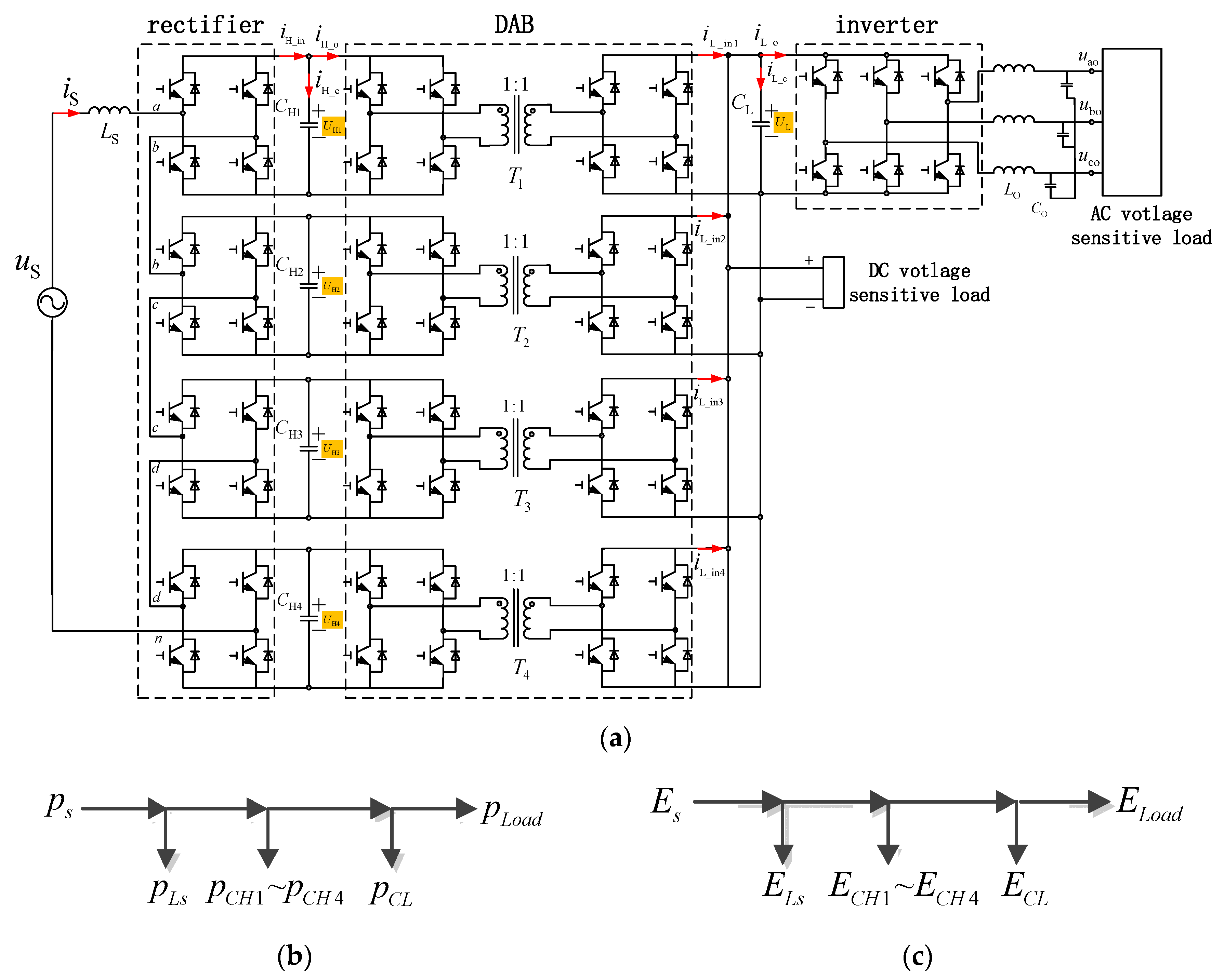
2. Mathematical Model of the PET

The topology of the single-phase PET is shown in Figure 2a, which contains a single-phase rectifier composed of four cascaded H-bridges, four dual active bridges (DAB) in parallel, and a three-phase inverter. The instantaneous power relationship in PET is shown in Figure 2b. The energy flow in PET is shown in Figure 2c.
The single-phase rectifier consists of an input inductor LS and four H-bridge modules. Each module uses the same modulation method. The drj is the duty cycle of the module j and the UHj is the CDB voltage of the module j (j = 1, 2, 3, 4). Ignoring the internal impedances of the inductor and the converters, the cascaded rectifier model can be described as
{ L s d i S d t = u S d r 1 U H 1 d r 2 U H 2 d r 3 U H 3 d r 4 U H 4 C H 1 d U H 1 d t = d r 1 i S U H 1 Z / 4 C H 2 d U H 2 d t = d r 2 i S U H 2 Z / 4 C H 3 d U H 3 d t = d r 3 i S U H 3 Z / 4 C H 4 d U H 4 d t = d r 4 i S U H 4 Z / 4
where Z is the equivalent impedance of the cascaded rectifier.
Ignoring the DAB internal impedances, the transmitted power of the DAB PDAB is
P D A B = n U H U L d ( 1 d ) 2 f s L s = k U H U L
where Ls is the HFT leakage inductance, UH is the primary dc voltage, UL is the second dc voltage, n is the transformer turns ratio, fs is the switching frequency, d is the duty cycles, and k = nd(1 − d)/2fsLs is the phase shift ration. When d equals 0.5, the PDAB is the maximum, and when d equals 1 or 0, the PDAB is zero.
The three-phase inverter model is not the focus of this paper. Here, the load Z is used for replacing the equivalent impedance of the ac load and the dc load. So, the average model of the single-phase PET is given in Figure 3, where k1~k4 are the phase shift ratios of the four DAB modules.
For improving the transient performance of the PET, the CDB voltage and the LDB voltage in the PET should be controlled. In Figure 2a, the four CDB voltages (UH1, UH2, UH3, and UH4) and the LDB voltage (UL) should reach their reference as quickly as possible during the transient process. At the same time, in the real system, every H-bridge model is designed to be identical in order to reduce the production consumption and the control complexity. However, the leakage inductance variation of the HFTs can reach 10–20% [14], and the transmitted power variation will also be 10–20%. In extreme cases, if the voltage balance control among the four cascaded modules is not adopted, the dc bus voltage of the DAB module with the largest leakage inductance will be four times the normal dc bus voltage, while the dc bus voltages of the other modules will reduce to nearly 0, which is absolutely unacceptable.
So, the stability of two-stage bus voltages in the topology is very important, especially for the voltage-sensitive loads, such as the data server, the navigation and positioning instrument, and so on. In this paper, Section 3 and Section 4 have a parallel relationship. In Section 3, the energy balance relationship around the low-voltage bus is deduced, and the control law and its stability analysis are also introduced in detail. Moreover, in Section 4, the energy balance relationship with the cascade buses is deduced, the stability and the control law for the cascaded voltage balance are analyzed, and the influence of the parameter range of the passive components in the model is analyzed for the control law performance.

3. Energy Balance Control for LDB Voltage

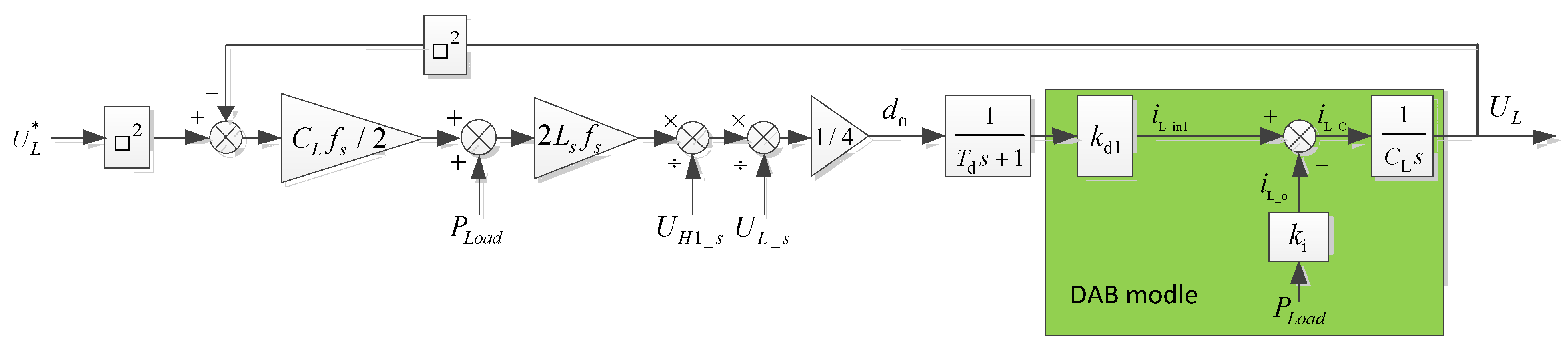
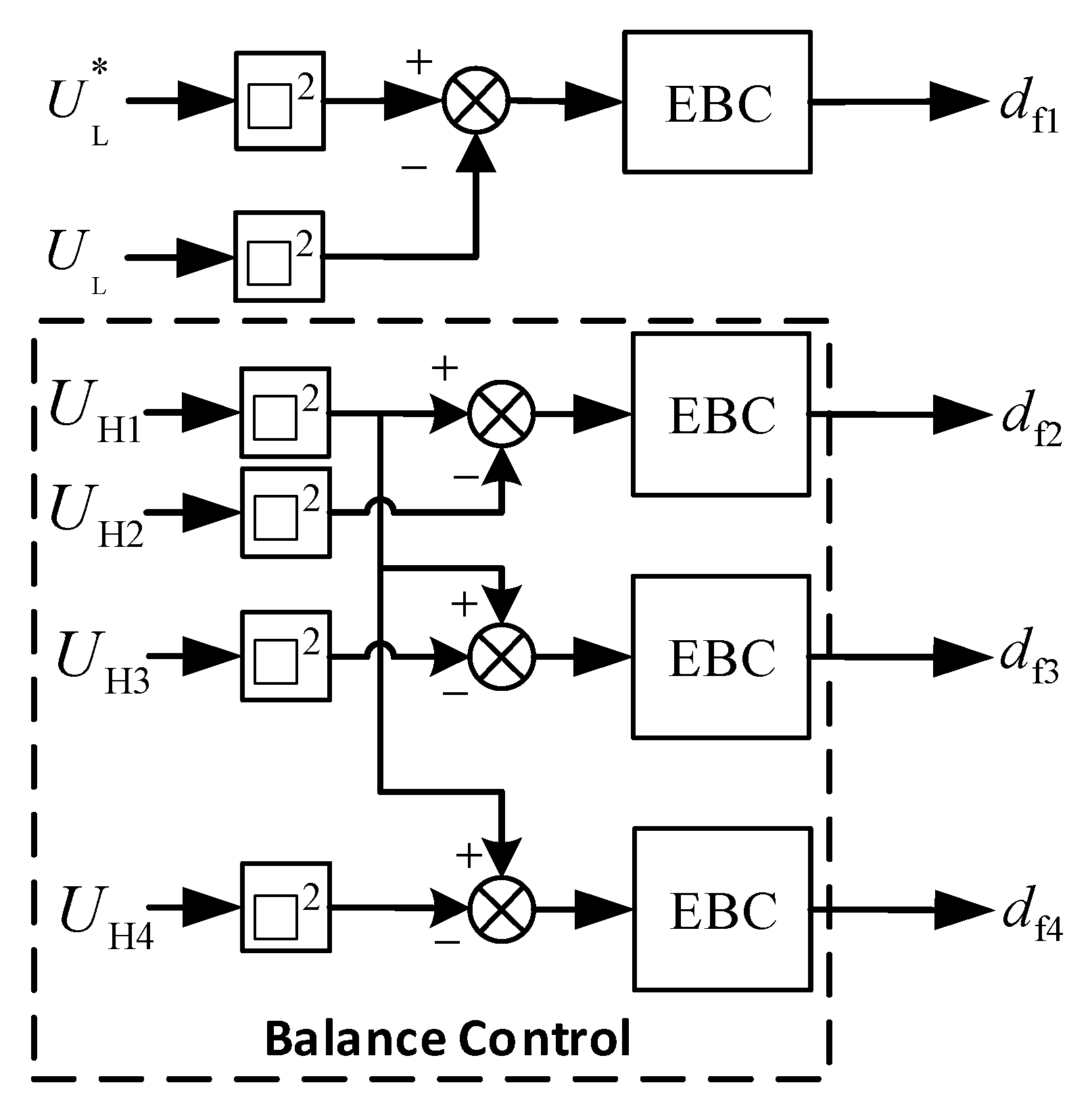
3.1. Energy Balance Control Scheme for DAB

Based on the equivalent circuit in Figure 3 and the energy relationship in Figure 2c, the energy relationship between the DAB, the LDB capacitor, and the equivalent load can be described as
E D A B = E C L + E L o a d
where the four DAB transmitted energies are regarded as the same under the voltage balance control. Considering the energy relationship in one switching period, it can be written as
P D A B = 1 2 C L ( U L * 2 U L 2 ) / T s + P L o a d
where Ts is the switching period, fs = 1/Ts.
Then, the total energy relationship becomes
4 × n U H _ s U L _ s d ( 1 d ) 2 f s L s = 1 2 C L ( U L * 2 U L 2 ) / T s + P L o a d
where UH_s and UL_s are the expectation values of the CDB and the LDB voltage. After simplification and approximation, the duty cycle d for the DAB is
d = ( 1 2 C L ( U L * 2 U L 2 ) f s + P L o a d ) × 2 f s L s 4 n U H _ s U L _ s
Considering the control delay of the DAB stage as a first-order inertial element with a constant time Td, the control scheme is depicted in Figure 4, and the DAB model is in the green block, where kd1 = nUH1/2fsLs1, ki = 1/UL.

3.2. Small-Signal Analysis

Performing small-signal decomposition of the system variables in Figure 4, we have
{ U L * = U ¯ L * + u ˜ L * U L = U ¯ L + u ˜ L P L o a d = P ¯ L o a d + P ˜ L o a d
where U ¯ L * is the reference of the LDB voltage, U ¯ L is the real value of the LDB voltage, and P ¯ L o a d is the real value of the load power. These values are the large-signal component. u ˜ L * , u ˜ L , and P ˜ L o a d are the small-signal values of the counterparts. The square values of the small signals are small enough to be ignored. The small-signal expression of the duty cycle is
d ˜ = ( 1 2 C L ( U ¯ L * u ˜ L * U ¯ L u ˜ L ) f s + P ˜ L o a d ) × 2 f s L s 4 n U H _ s U L _ s
The corresponding small-signal control model is given in Figure 5.
The closed-loop transfer function of the LDB voltage control system based on EBC is
G d c _ L ( s ) = u ˜ L u ˜ L * = f s U ¯ L * U H 1 _ s 8 π ( T d s + 1 ) s + U H 1 _ s f s U ¯ L
From (9), it can be seen that the LDB voltage is irrelevant to the dc bus capacitance CL. Considering that the expectation value of the CDB voltage UH1_s and the LDB voltage UL_s remains constant, the load power P ˜ L o a d fluctuation in the DAB model is counteracted by the load power fluctuation, including in the feed-forward terms in the EBC. So, the load power fluctuation has no impact on the dc bus voltage, as is shown in Figure 5.
When the system adopts the low-bandwidth PI controller, the small-signal control model is as depicted in Figure 6.
The closed-loop transfer function of the LDB voltage control system based on the PI controller is
G d c _ L ( s ) = u ˜ L u ˜ L * = ( P 1 s + I 1 ) U H 1 _ s 8 π f s L s C L s 2 ( T d s + 1 ) + ( P 1 s + I 1 ) U H 1 _ s
From (10), it can be seen that the LDB voltage with the PI controller is affected by the capacitance CL. When UH1_s remains constant, from Figure 6, the dc bus voltage is affected by the load power P ˜ L o a d fluctuation. The closed-loop transfer functions are
G d p _ L ( s ) = u ˜ L P ˜ L o a d = 8 π f s L s ( T d s + 1 ) s 8 π f s L s C L s 2 ( T d s + 1 ) U L _ s + ( P 1 s + I 1 ) U H 1 _ s U L _ s
It is shown that compared with the PI controller, the EBC controller can eliminate the impacts of the LDB capacitor and the fluctuations of the load power by importing the load power into the control model. The robustness of the EBC is increased.

3.3. Stability Analysis

The stability analysis of the EBC closed-loop transfer function for the LDB voltage was conducted. The switching period is set as Ts = 5 × 10⁻⁵ s. Considering the sampling and the control delay, Td = 2Ts, the LDB voltage reference U ¯ L * is 700 V and the CDB voltage expectation value U H 1 _ s is 700 V. When the LDB voltage U ¯ L changes from 400 V to 1000 V, the denominator of Equation (9) has two poles. The two poles are far away from the origin, with the increasing of the voltage value, as shown in Figure 7. This figure shows that all the poles are located in the left half plane, and so, the system is stable.

4. Energy Balance Control for CDB Voltage

4.1. Derivation of CDB Average Voltage Reference

Based on the equivalent model in Figure 3 and the instantaneous power relationship in Figure 2b, the instantaneous power relationship of the PET is as follows:
p s = p L s + p C H 1 + p C H 2 + p C H 3 + p C H 4 + p C L + p L o a d
In the steady state, the voltages in the cascade bus capacitors are equal, and the instantaneous powers of the cascaded capacitors are also same, namely PHC1 = PCH2 = PCH3 = PCH4 = PCH; Equation (12) can be simplified as
p s = p L s + 4 p C H + p C L + p L o a d
Assume that the grid voltage and current are
u s = 2 U s sin ( ω t )
i s = 2 I s sin ( ω t + θ )
where Us and Is are the RMS values of the grid voltage and current, ω is the grid angular frequency, and θ is the initial phase angle of grid current.
Thus, the instantaneous power of the grid is
p s = u s i s = U s I s [ cos θ cos ( 2 ω t + θ ) ] = P s U s I s cos ( 2 ω t + θ )
where the dc component is the constant power of the grid, and it is expended by the load. The second harmonic power of the grid will cause the second harmonic voltage ripple in the CDB voltages.
The instantaneous power of the input inductors is
p L s = L s d i s d t i s = L s I s 2 sin ( 2 ω t + 2 θ ) ω
The whole instantaneous power of the four cascaded capacitors is
4 p C H = 4 C H d U H d t U H
The instantaneous power of the capacitors in the LDB is
p C L = C L d U L d t U L
In the steady state, the LDB voltage UL is constant, then PCL = 0.
The load power equals the grid constant power.
P s = p L o a d
The phase of the grid voltage and current are set to be the same value. Substituting (14)~(20) into (13), it becomes
4 C H d U H d t U H + A cos ( 2 ω t φ ) = 0
where
A = I s U s 2 + ( L a c I s ω ) 2 φ = arctan L a c I s ω U s
Then, the average reference of the CDB voltage is
U H * = U H a v e * 2 B B = A 4 C H ω sin ( 2 ω t φ )
where B is the square value of the second harmonic voltage amplitude of the CDB voltage.

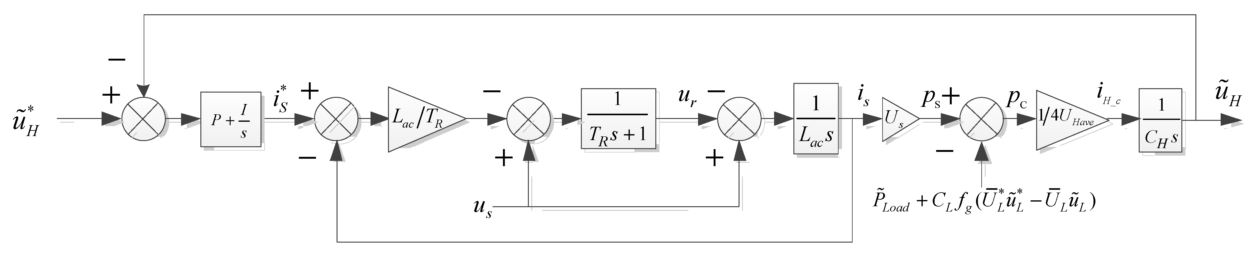
4.2. Energy Balance Control Scheme for Rectifier

Based on the equivalent model in Figure 3 and the energy relationship in Figure 2c, the energy relationship is as follows:
E s = E L s + 4 E C H + E C L + E L o a d
According to the analysis of the two-stage, single-phase photovoltaic grid-connected inverters [17], for the single PWM rectifier, when the system is in steady state, the absolute value of the grid current remains constant after half line cycle Tg/2; then, the stored energy of the filter inductor also remains constant after Tg/2, namely ELs = 0. When ignoring the internal impedances of the PET, the energy relationship of the PET in Tg/2 is
T g 2 P L o a d + 1 2 4 C H ( U H * 2 U H 2 ) + 1 2 C L ( U L * 2 U L 2 ) = U s I s * T g 2
Thus, the grid current reference is
I s * = P L o a d + 4 C H f g ( U H * 2 U H 2 ) + C L f g ( U L * 2 U L 2 ) U s
Considering the control delay of the rectifier stage as a first-order inertial element with a constant time TR, the control scheme is depicted in Figure 8, and the rectifier model is in the green block, where kg = 4CHfg, kT = 1/US, PR = Lac/TR, ur = 4dUH, and kR = US/4UH.

4.3. Small-Signal Analysis

In the condition that the calculated value B is consistent with the actual second harmonic voltage ripple, and the equivalent load power in the CDB side is replaced by the load power in the LDB side, the EBC control model can be depicted as shown in Figure 9.
Performing small-signal decomposition of the system variables in Figure 9, we have
{ I s * = I ¯ s * + i ˜ s * U H * = U ¯ H * + u ˜ H * U H = U ¯ H + u ˜ H P L o a d = P ¯ L o a d + P ˜ L o a d U L * = U ¯ L * + u ˜ L * U L = U ¯ L + u ˜ L
where I ¯ s * is the grid current, U ¯ H * is the reference of the CDB voltage, U ¯ H is the real value of the CDB voltage, U ¯ L * is the reference of the LDB voltage, U ¯ L is the real value of the LDB voltage, and P ¯ L o a d is the real load power. These values are the large-signal component. i ˜ s * , u ˜ H * , u ˜ H , u ˜ L * , u ˜ L , and P ˜ L o a d are the variation in the transient process; these variations are the small-signal values of the counterparts. The square values of the small signals are small enough to be ignored. The small-signal expression of the current reference is
i ˜ s * = P ˜ L o a d + 4 C H f g ( U ¯ H * u ˜ H * U ¯ H u ˜ H ) + C L f g ( U ¯ L * u ˜ L * U ¯ L u ˜ L ) U s
The corresponding small-signal model is shown in Figure 10.
The closed-loop transfer function of the CDB voltage control system based on the EBC controller is
G d c _ H ( s ) = u ˜ H u ˜ H * = f g U ¯ H * [ T R s ( T R s + 1 ) + 1 ] U H a v e s + f g U ¯ H
It can be seen that the CDB voltage is irrelevant to the dc bus capacitance CH. Considering that the grid voltage Us remains constant, the load power P ˜ L o a d fluctuation in the rectifier model and the stored energy fluctuation of the LDB capacitor are counteracted by the same power fluctuation, including in the feed-forward terms in the EBC. So, the fluctuation of the load power and the LDB capacitor power have no impact on the dc bus voltage, as shown in Figure 10.
When the system adopts the low-bandwidth PI controller, the small-signal model is as depicted in Figure 11.
The closed-loop transfer function of the CDB voltage control system based on the PI controller is
G d c _ H ( s ) = u ˜ H u ˜ H * = ( P s + I ) U S 4 s 2 U H a v e C H [ T R s ( T R s + 1 ) + 1 ] + ( P s + I ) U S
It can be seen that the CDB voltage with the PI controller is affected by the capacitance CH. When the grid voltage US remains constant, the dc bus voltage is affected by the load power P ˜ L o a d fluctuation, the capacitance on the LDB side CL, and the LDB voltage fluctuation u ˜ L * . The closed-loop transfer functions are
G d p _ H ( s ) = u ˜ H P ˜ L o a d = [ T R s ( T R s + 1 ) + 1 ] s 4 s 2 U H a v e C H [ T R s ( T R s + 1 ) + 1 ] + ( P s + I ) U S
G d i _ H ( s ) = u ˜ H u ˜ L * = C L f g U ¯ L * [ T R s ( T R s + 1 ) + 1 ] s 4 s 2 U H a v e C H [ T R s ( T R s + 1 ) + 1 ] + ( P s + I ) U S
It can be concluded that compared with the PI controller, the EBC controller can eliminate the impacts of the CDB capacitors and the fluctuations of the load power and the power of the LDB capacitor by importing their power into the control structure. The robustness of the EBC for the CDB voltage is increased.

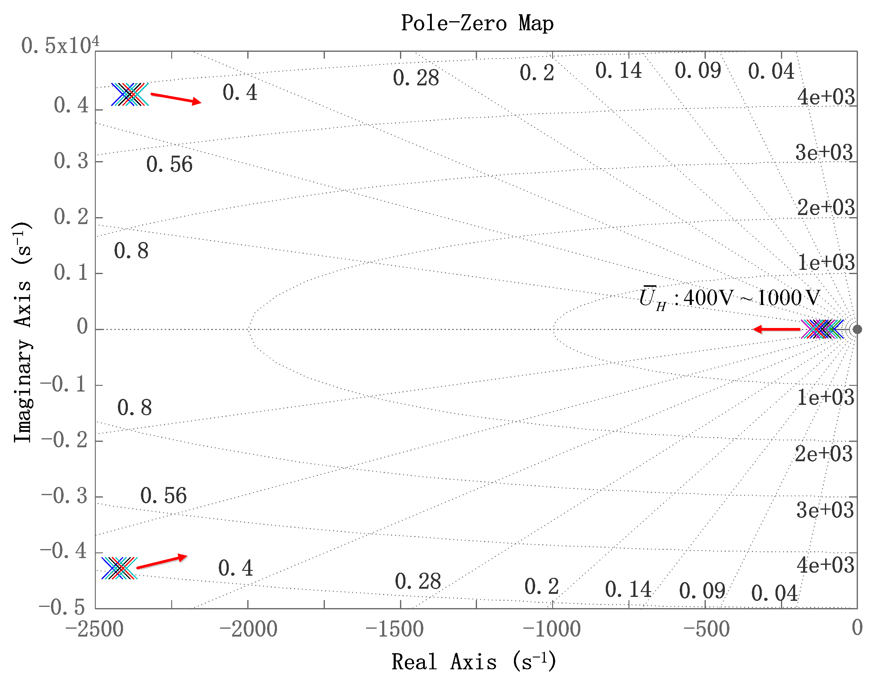
4.4. Stability Analysis

The stability analysis of the EBC closed-loop transfer function for the CDB voltage was conducted. The switching period is set as Ts = 1 × 10⁻⁴ s. Considering the sampling and the control delay, TR = 2Ts, the grid frequency fg = 50 Hz, and the dc bus voltage reference UHave = 700 V. When the dc bus voltage U ¯ H changes from 400 V to 1000 V, the denominator of Equation (29) has three poles. Two poles are far away from the origin and the other one is the dominant pole, moving away from the origin with the increasing of the voltage value, as is shown in Figure 12. This figure shows that all the poles are located in the left half plane, and the system is stable.

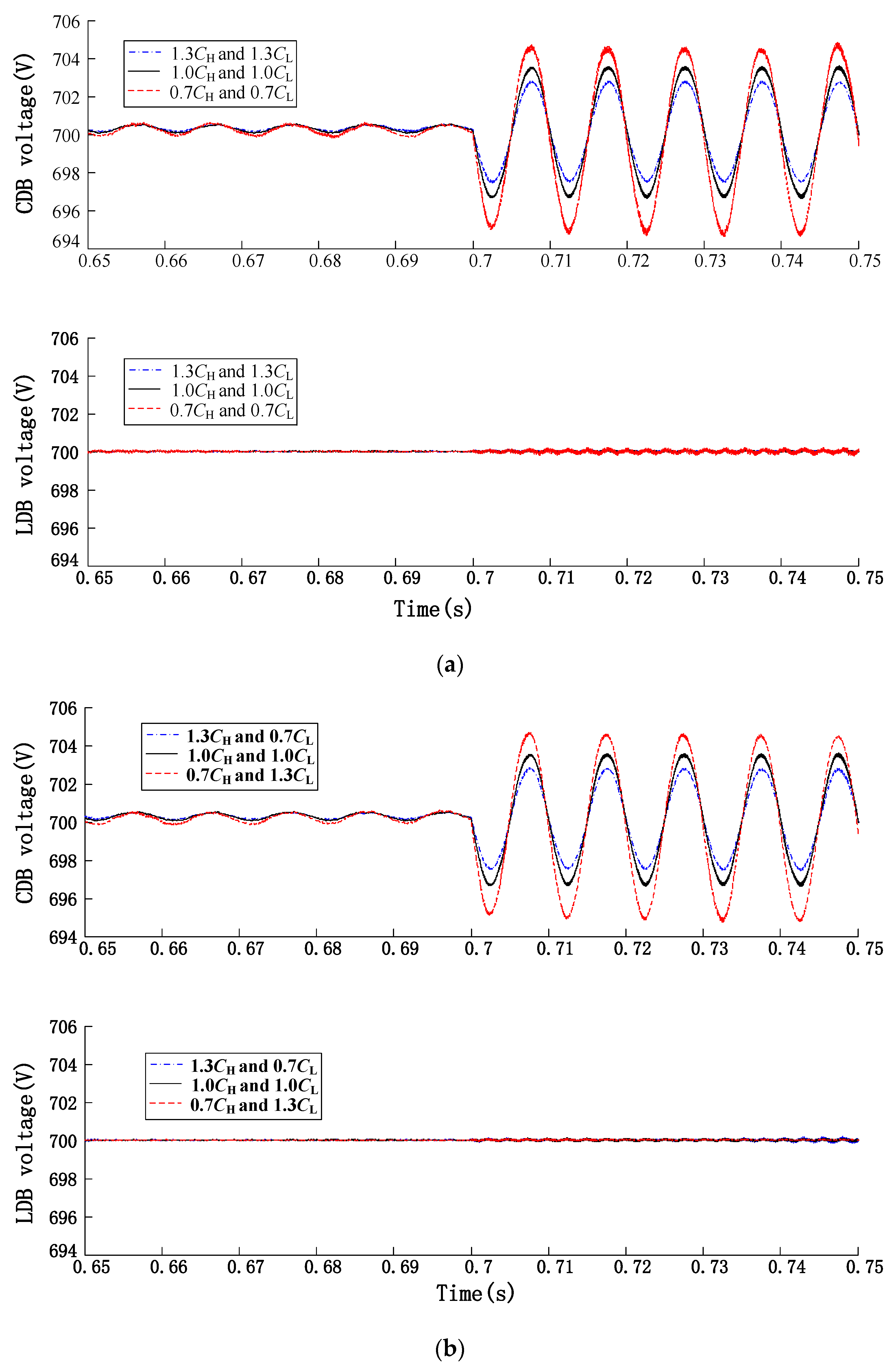
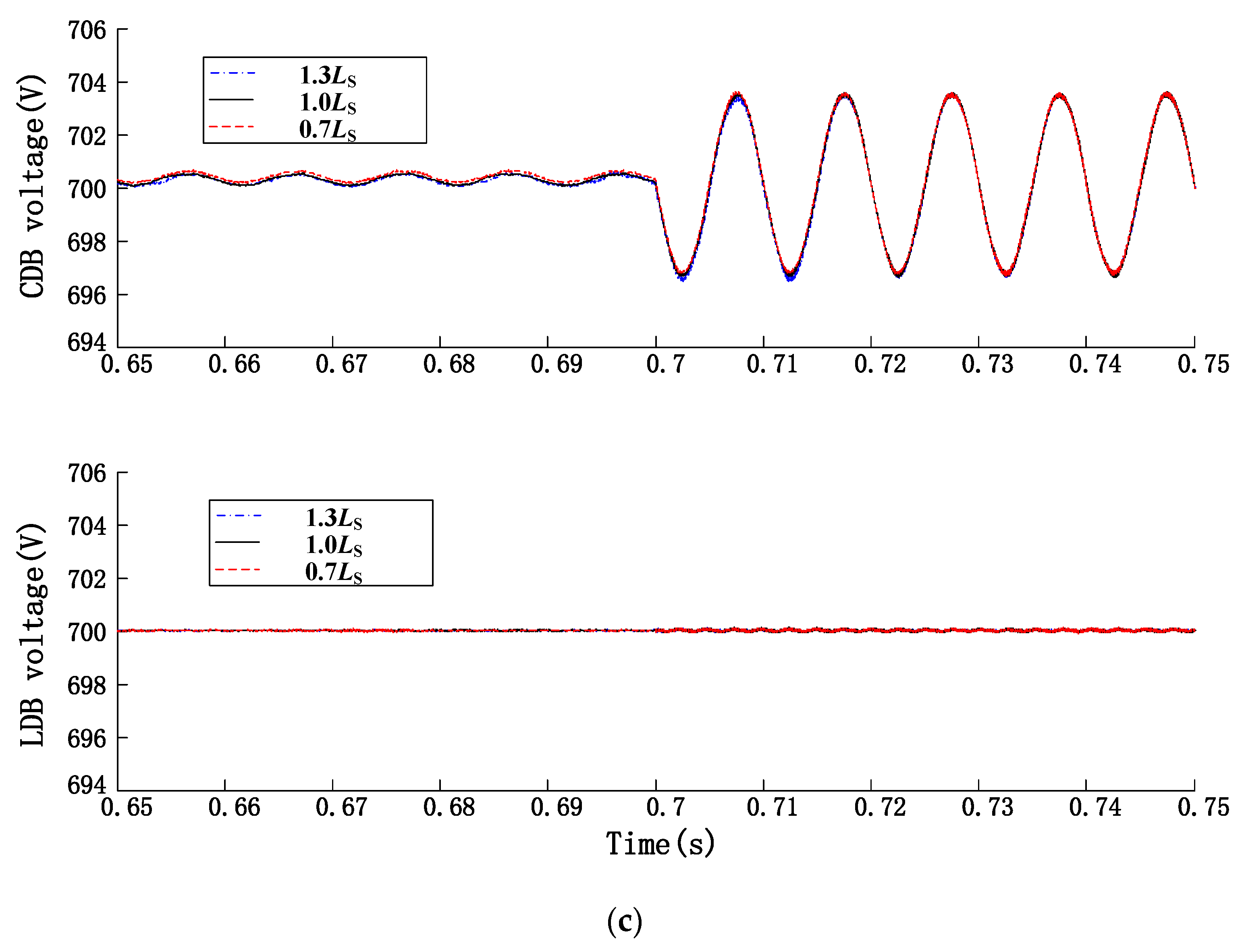
4.5. Adaptability Analysis of Model Parameter

When EBC control mode is adopted, the parameter deviation of the passive components in the model has limited influence on the control effect. In the simulation shown in Figure 13a, the load power increases rapidly from 1.4 kw to 28 kw at 0.7 s, when the capacitance value of two-stage bus has the same direction deviation of ±30%. From the simulation waveform, it can be seen that the voltage of the cascade bus basically does not overshoot in the dynamic process, and the maximum difference of the intermediate bus voltage in the steady-state process is within 2 V, which is consistent with the relationship between the capacitance value of the intermediate bus and the ripple amplitude of the secondary voltage in Formula (23). At the same time, the difference of the capacitance value will affect the average value of the bus voltage. There is almost no overshoot of low-voltage bus voltage in the dynamic process. In the steady state, the bus voltage fluctuates slightly with the increase in power, but the fluctuation value is very small and can be ignored.
As shown in Figure 13b, when the capacitance value of the two-stage bus has a reverse deviation of ±30%, the simulation waveform of the bus voltage is similar to that with the same deviation. It shows that EBC has good adaptability to capacitance parameter deviation, but the ripple of the steady-state process is affected, and the dynamic performance is not affected.
As shown in Figure 13c, when the grid side inductance value deviates by ±30%, the CDB voltage and the LDB voltage have almost no overshoot in the dynamic process. It is verified that EBC has good adaptability to the inductance parameters, and the change of inductance parameters has no impact on the steady-state and dynamic control effects.

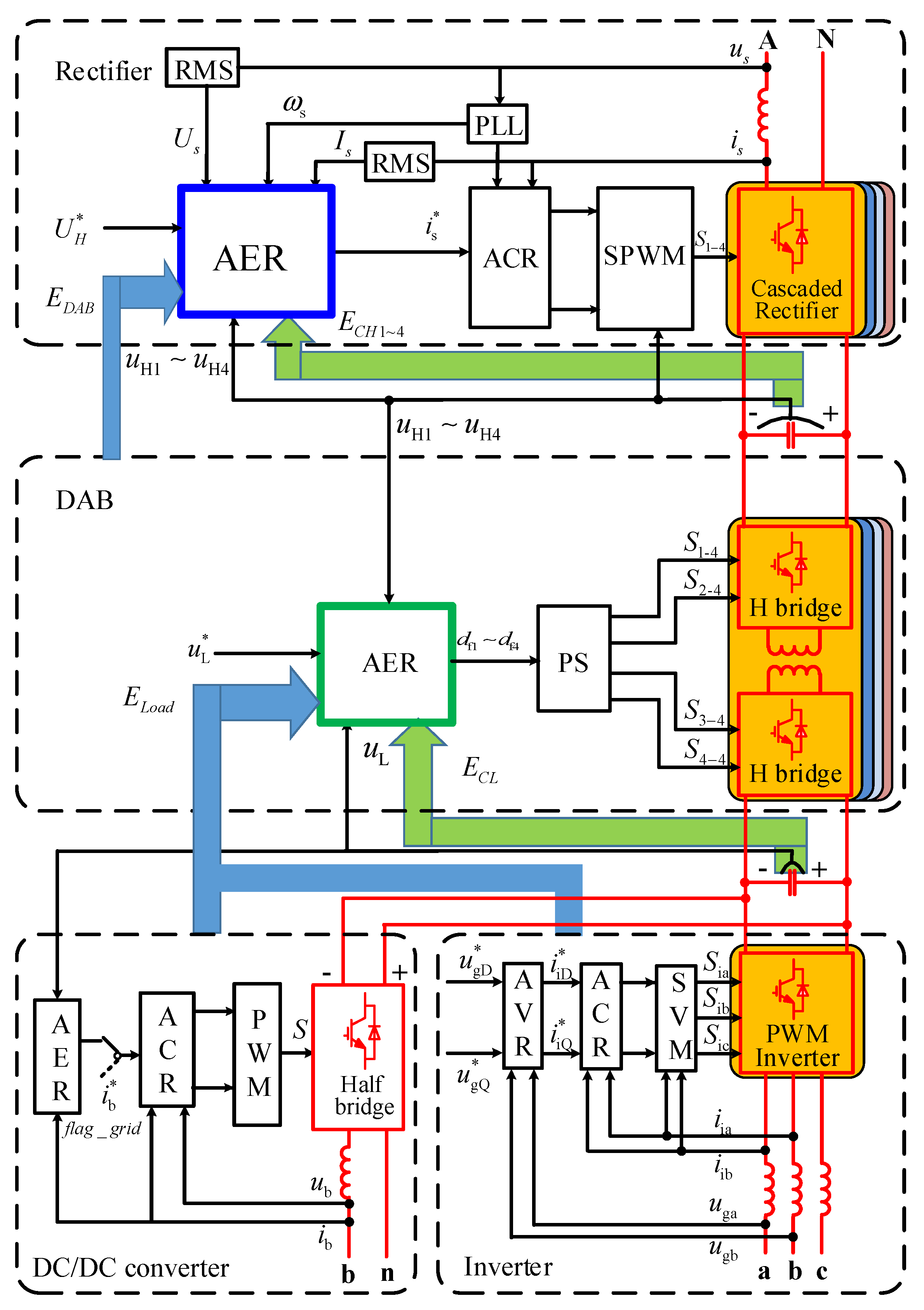
5. Overall Structure of Proposed Control Strategy

When the CDB voltages of each cascaded module are equal under the voltage balance control, and the duty cycles transmitted to each of the rectifier modules are the same, the received powers of each module are also equal. Therefore, when the CDB voltages are equal, the same duty cycle transmitted to each of the rectifier modules can conveniently ensure the power balance with a small error.
In the DAB controller, the first DAB module controls the LDB voltage, and the other three DAB modules control their respective primary side voltages to follow that of the first DAB module. The control scheme of the parallel DABs is shown in Figure 14; the four DAB modules adjust their respective duty cycle ( d f 1 , d f 2 , d f 3 , d f 4 ) and use the EBC to change the transmitted power and guarantee that the other three CDB voltages follow the first CDB voltage. The d f 1 is the phase shift control duty cycle of the first DAB module, and d f 2 , d f 3 , d f 4 are the phase shift control duty cycle of the second, third, and fourth DAB modules, respectively.
The cascaded rectifier modules adopt the same duty cycle for achieving the transmitted power balance. At the same time, the carrier phase shift is utilized to increase the equivalent switching frequency.
The energy balance control diagram of PET is revealed in Figure 15. In the rectifier, the control scheme adopts a double-loop control structure. The automatic energy regulator (AER) is used in the outer loop for controlling the CDB voltage, and the automatic current regulator (ACR) is used in the inner loop for controlling the grid current. In the DAB, the AER controls the LDB voltage and the CDB voltage balance, and the phase shift (PS) modulation is used in the DAB. For the inverter, the ordinary double-loop d-q decoupling control scheme is adopted. For the DC/DC converter, the ACR is used to control the output current or the output power when the PET is on the grid. In the off-grid state, the DC/DC converter is used to control the LDB voltage.

6. Simulation and Experimental Verification

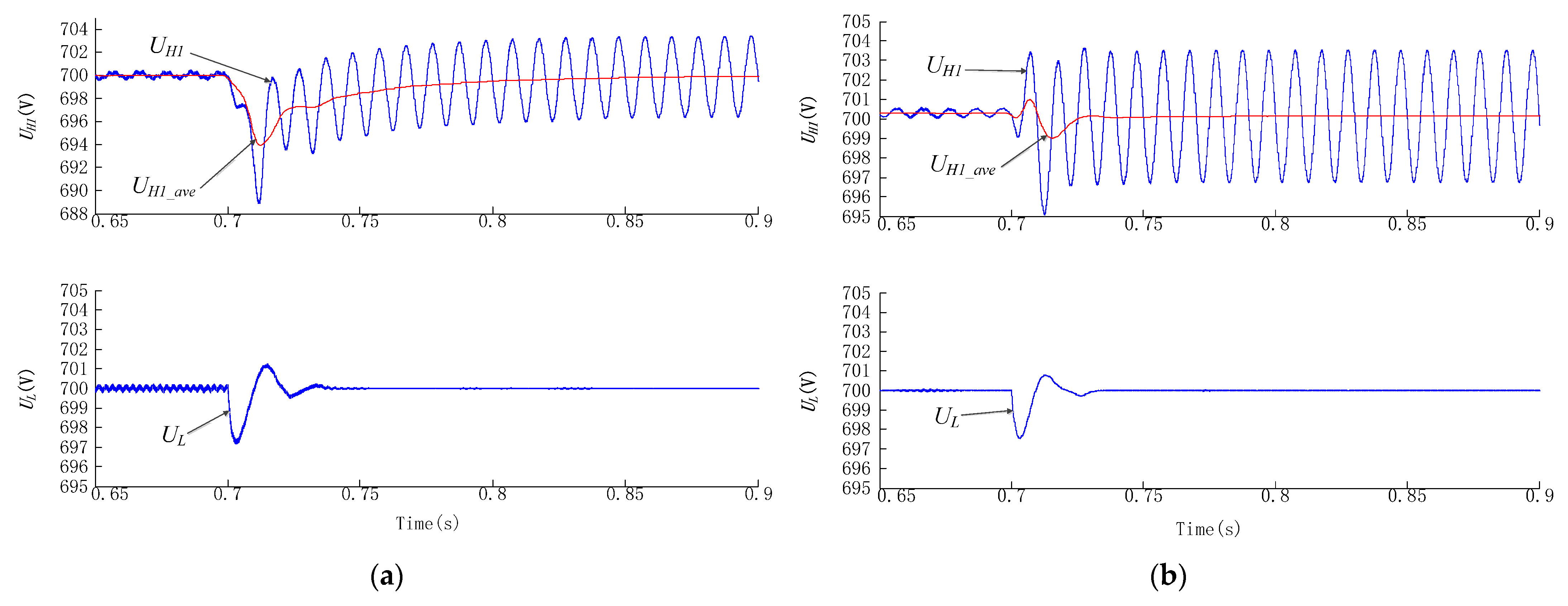
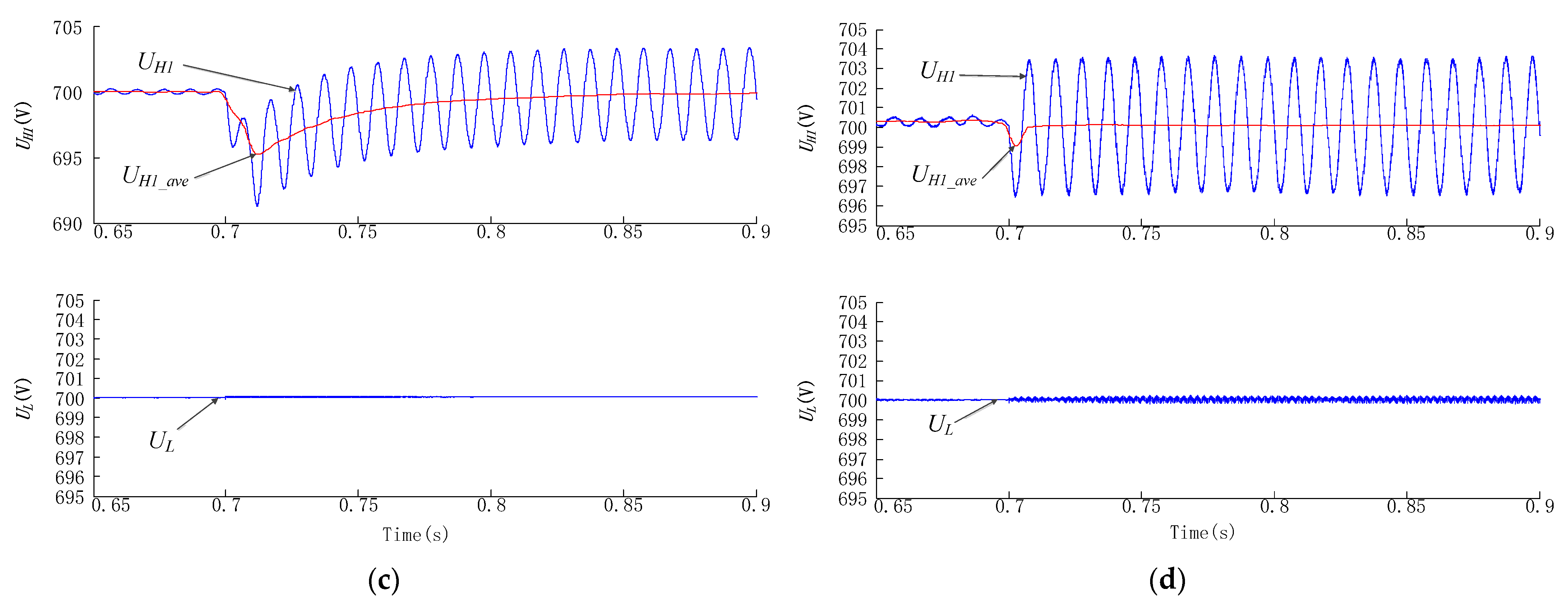
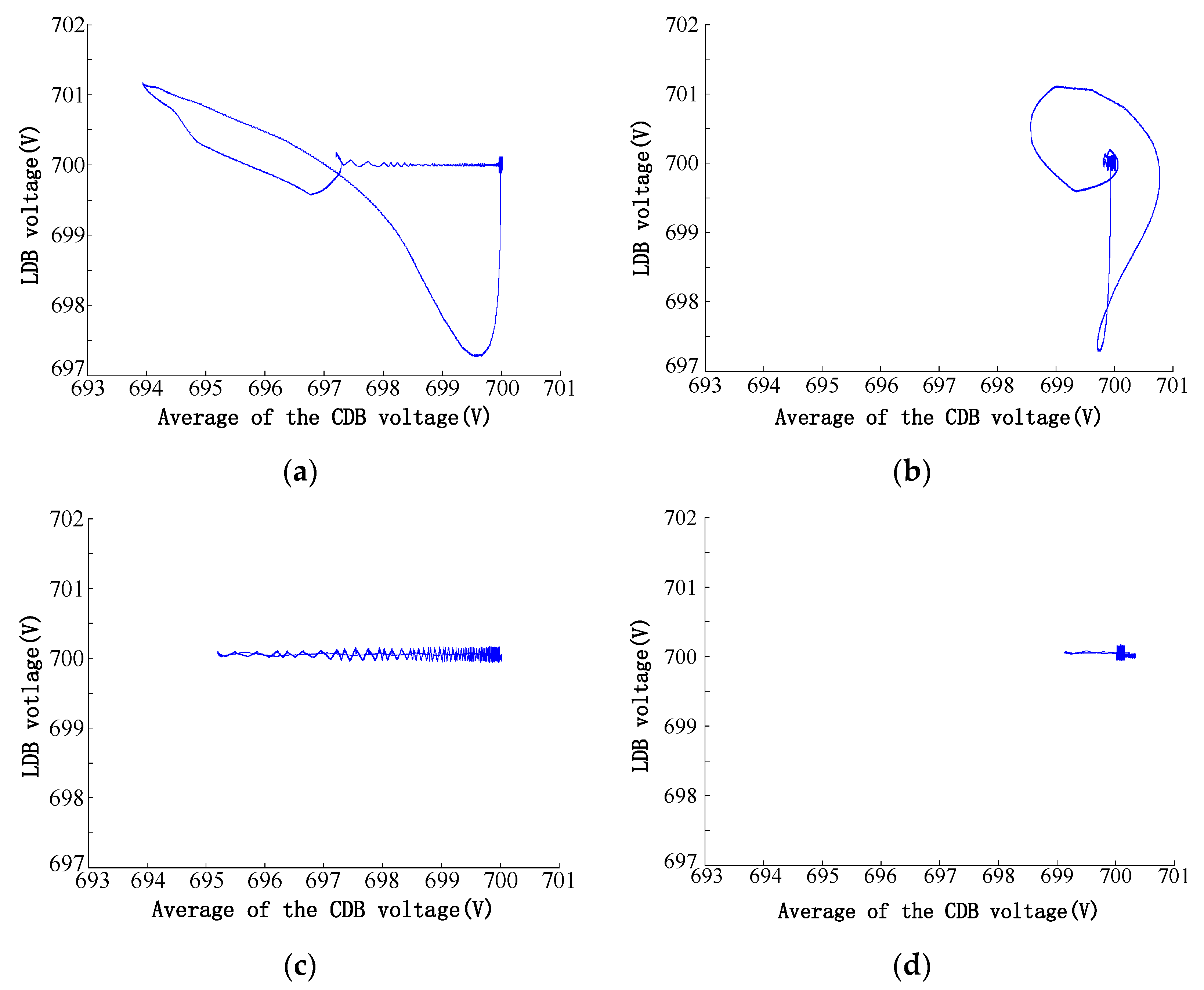
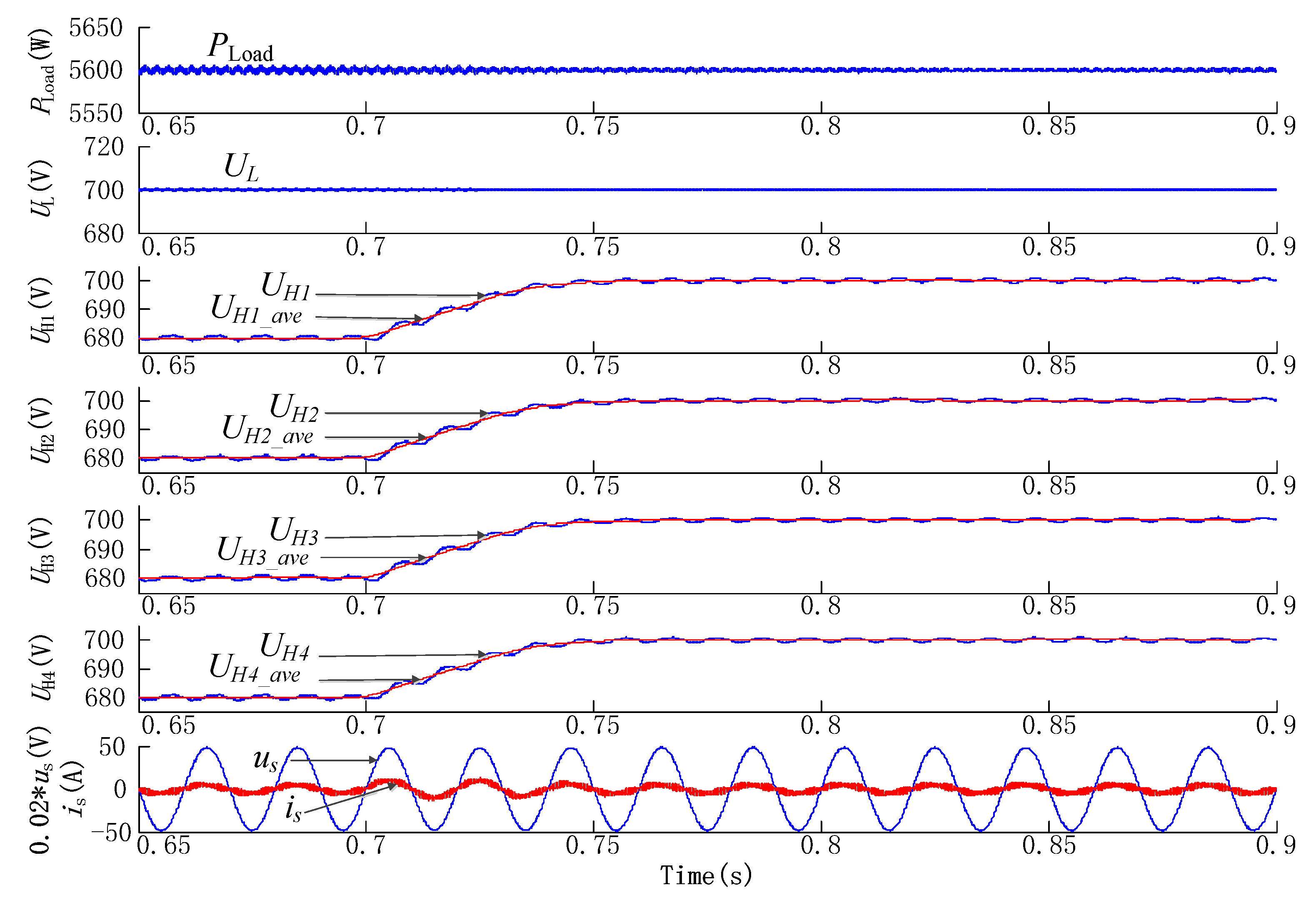
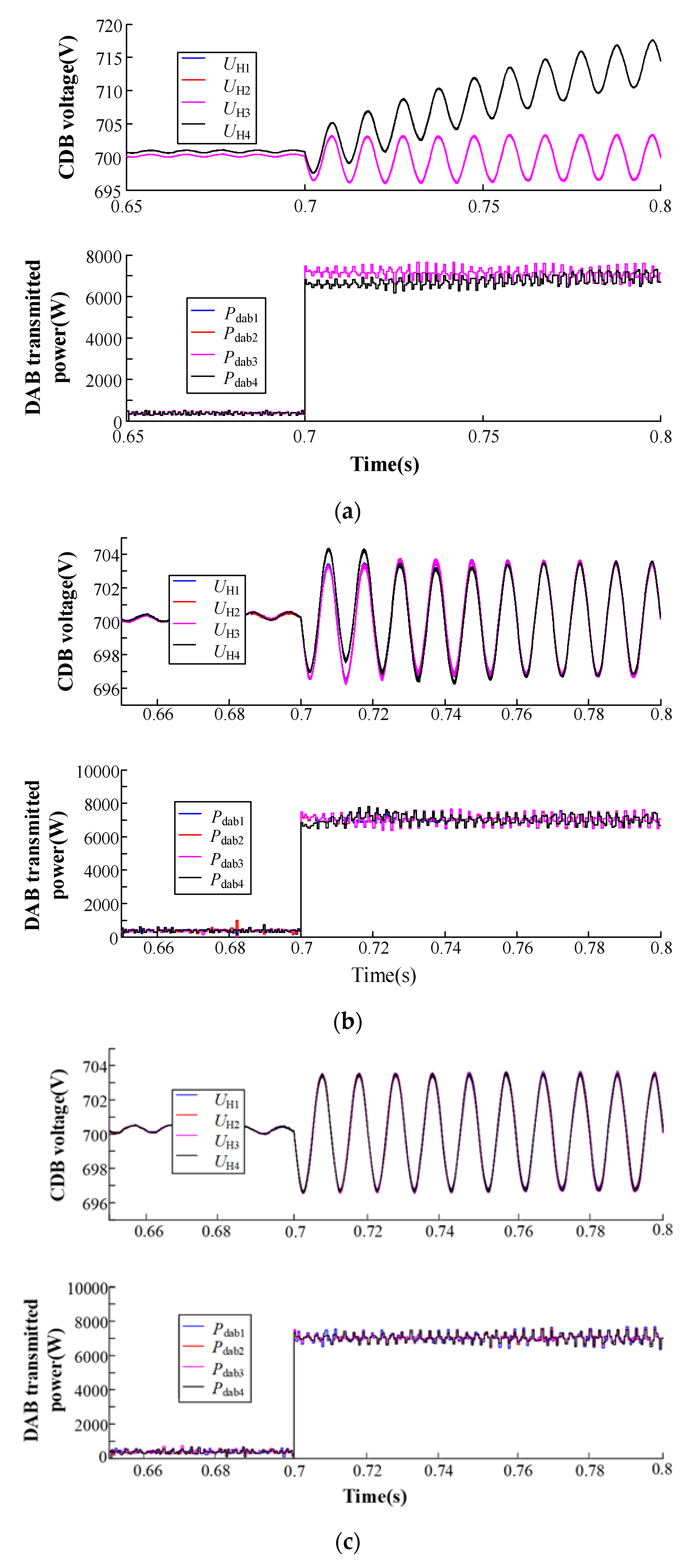
6.1. Simulation Results

As a comparison, the PI control scheme is used in the PET. In the CDB control loop, the voltage sampling values are filtered with a low-pass filter, whose bandwidth is 30 Hz. The simulation parameters are listed in Table 1.
When the CDB voltage is controlled by the EBC controller and the LDB voltage is controlled by the PI controller, the waveforms of the variables are as presented in Figure 16, in which the red curves UHx_ave represent the average values of the real voltage UHx. It is shown that the four CDB voltages are stable and balanced in the steady state, and this proves the effectiveness of the EBC scheme.
For the transient performance of the CDB voltages and the LDB voltage, Figure 17 demonstrates the waveforms of the UH1, UH1_ave, and the UL when the load power increases from 1.4 kW to 28 kW at 0.7 s, in which the PI controller and the EBC controller are used, respectively. The EBC control strategy can achieve a better transient performance than the PI controller, both in the CDB voltage and the LDB voltage, as is shown in Figure 17b,c. Two different time-scale EBC controllers used in two dc bus voltages simultaneously can realize the optimal transient performance, which has the minimum transient time and a very small overshoot, as is shown in Figure 17d.
The corresponding track of the time-domain waveform in the phase plane is shown in Figure 18, which is composed of the average of CDB voltage UH1_ave in the horizontal axis and the LDB voltage UL in the vertical axis. The smaller the area that is surrounded by the track in the figure means the smaller the change of the energy storage of the two-stage bus capacitance in the transient process, which means the smaller the voltage fluctuation. It can be found from the comparison that the transient performance of the two-stage dc bus voltage can be effectively improved by using EBC.
When the voltage reference changes from 680 V to 700 V at 0.7 s, the waveforms of the variables with the EBC controller are shown in Figure 19. It is shown that four CDB voltages are kept in good consistence whether in the steady state or the transient state.
To verify the voltage balance control effect in the different parameters of the DAB modules, the leakage inductance of the HFTs in the 4th DAB module is set to be 10% larger than the others in the simulation setup (Ls1 = Ls2 = Ls3 = 328 uH, Ls4 = 360 uH). The four CDB voltages and the parallel transmitted power are shown in Figure 20. It can be seen that when the voltage balance control is not adopted, the UH4 is out of control when the transmission power increases. When the PI controller is used for voltage balance control, the voltage and power balance of the four modules can be realized after a period of time. After adopting the EBC controller, the voltage balance speed of the four modules is accelerated, and the power in the four DAB modules can be quickly balanced.

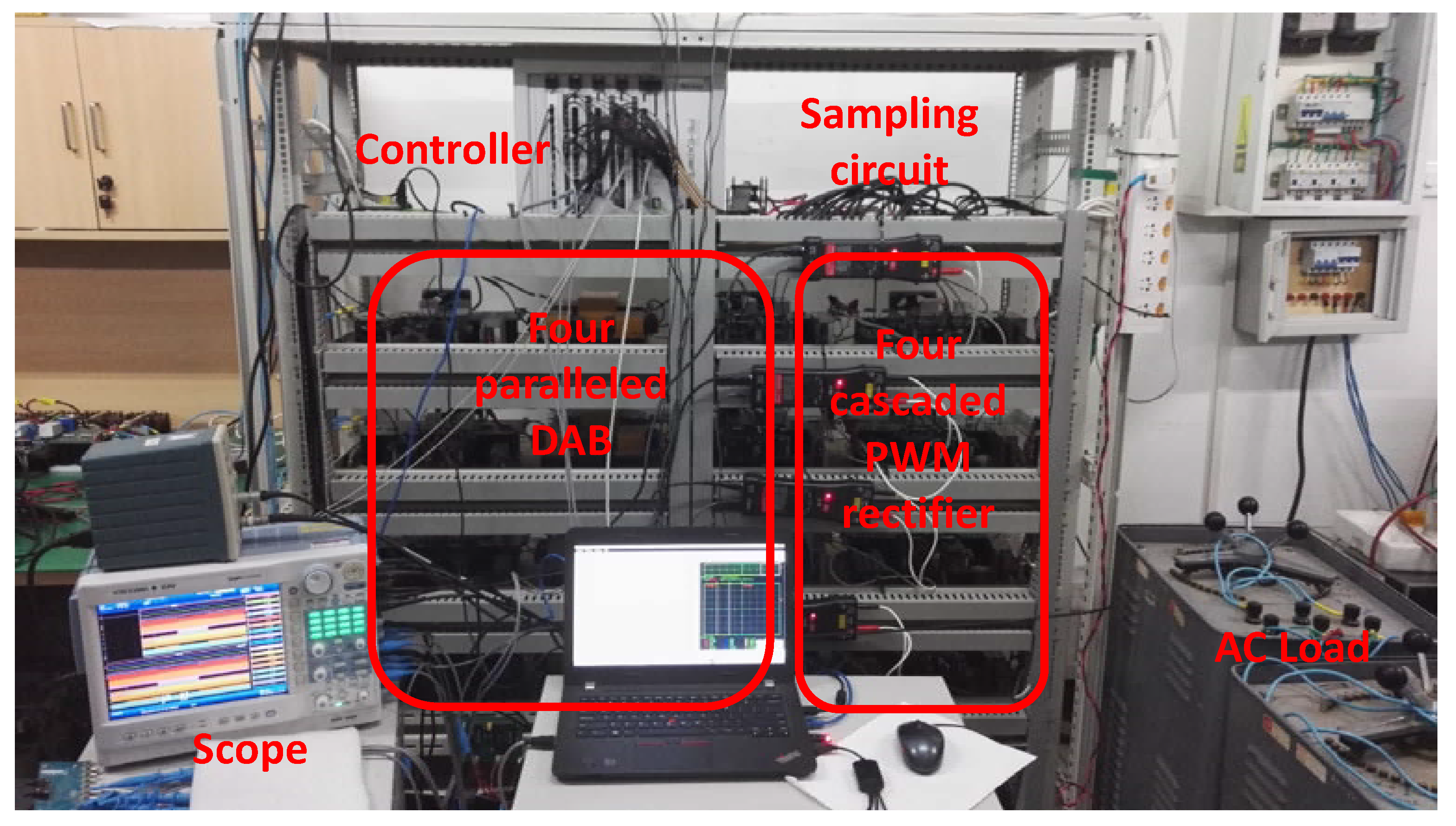
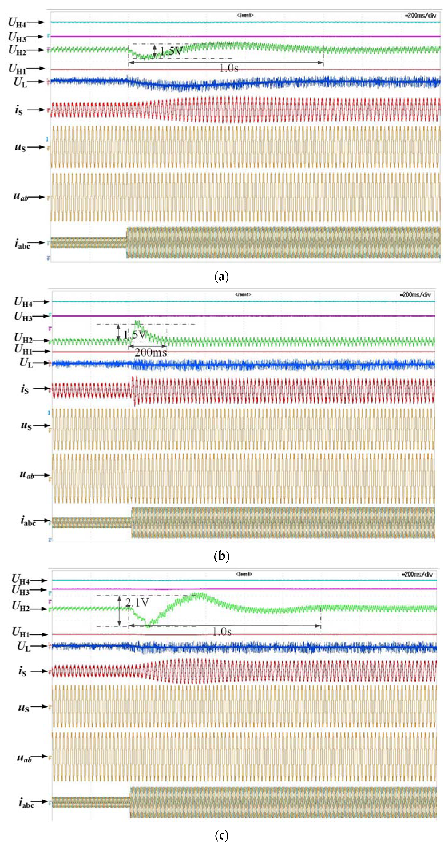
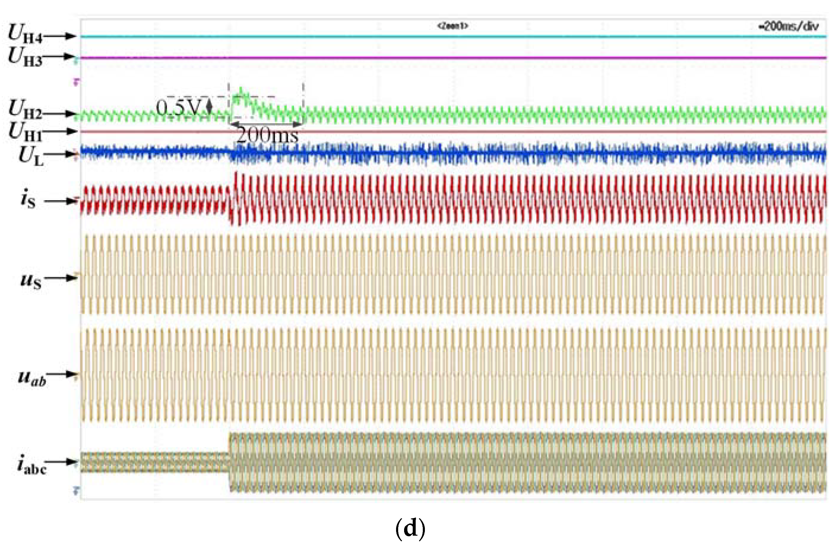
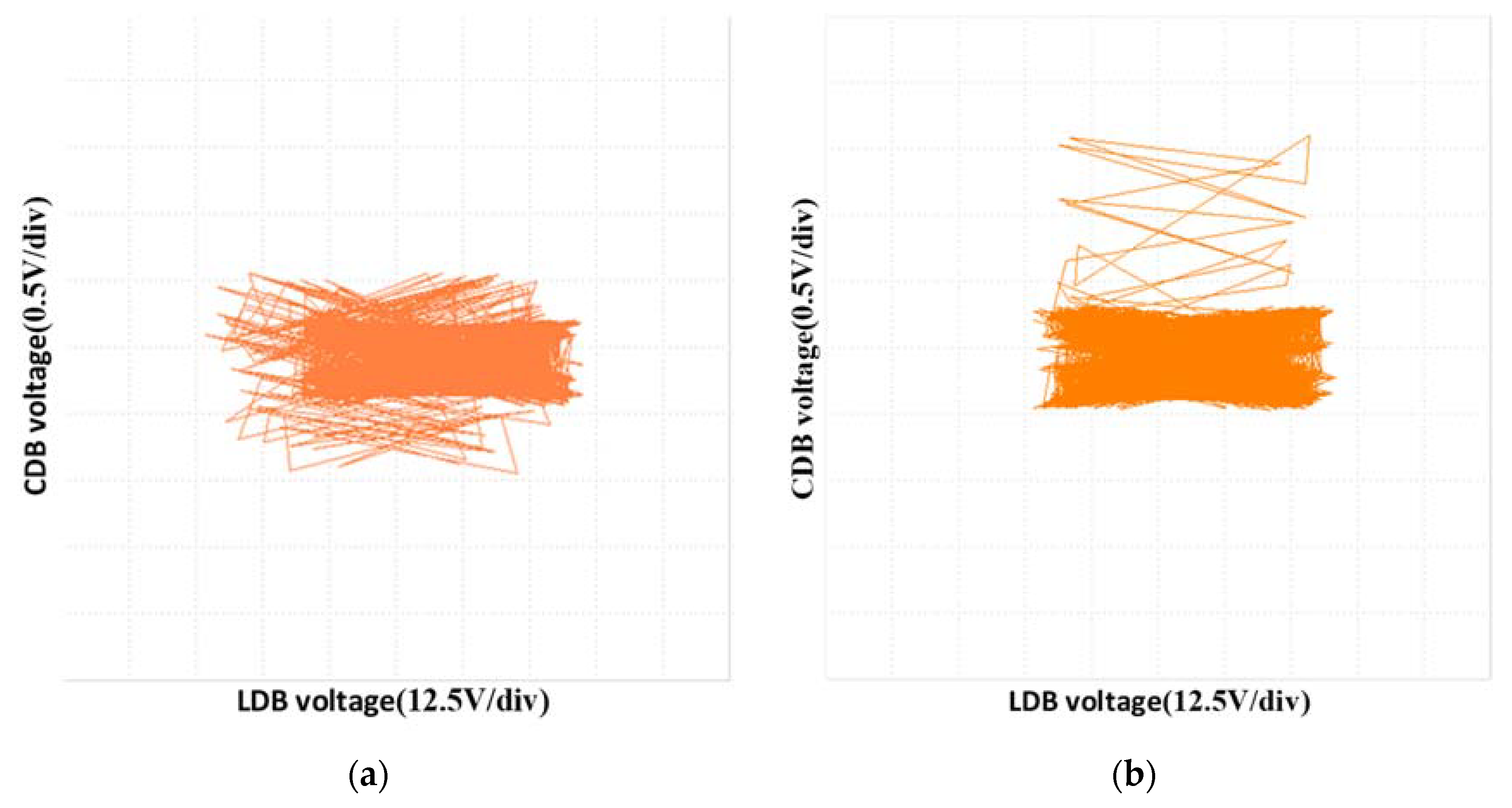
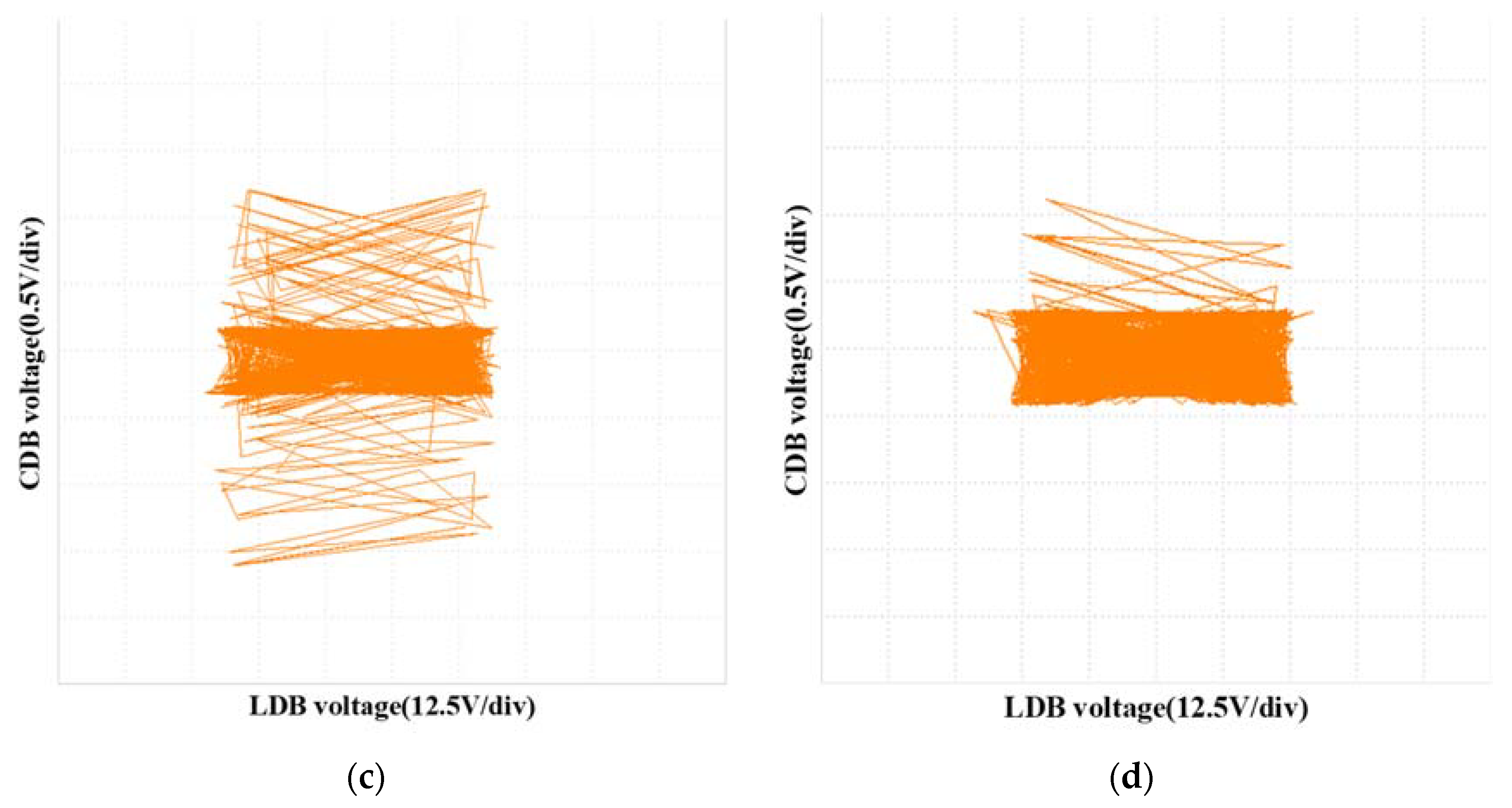
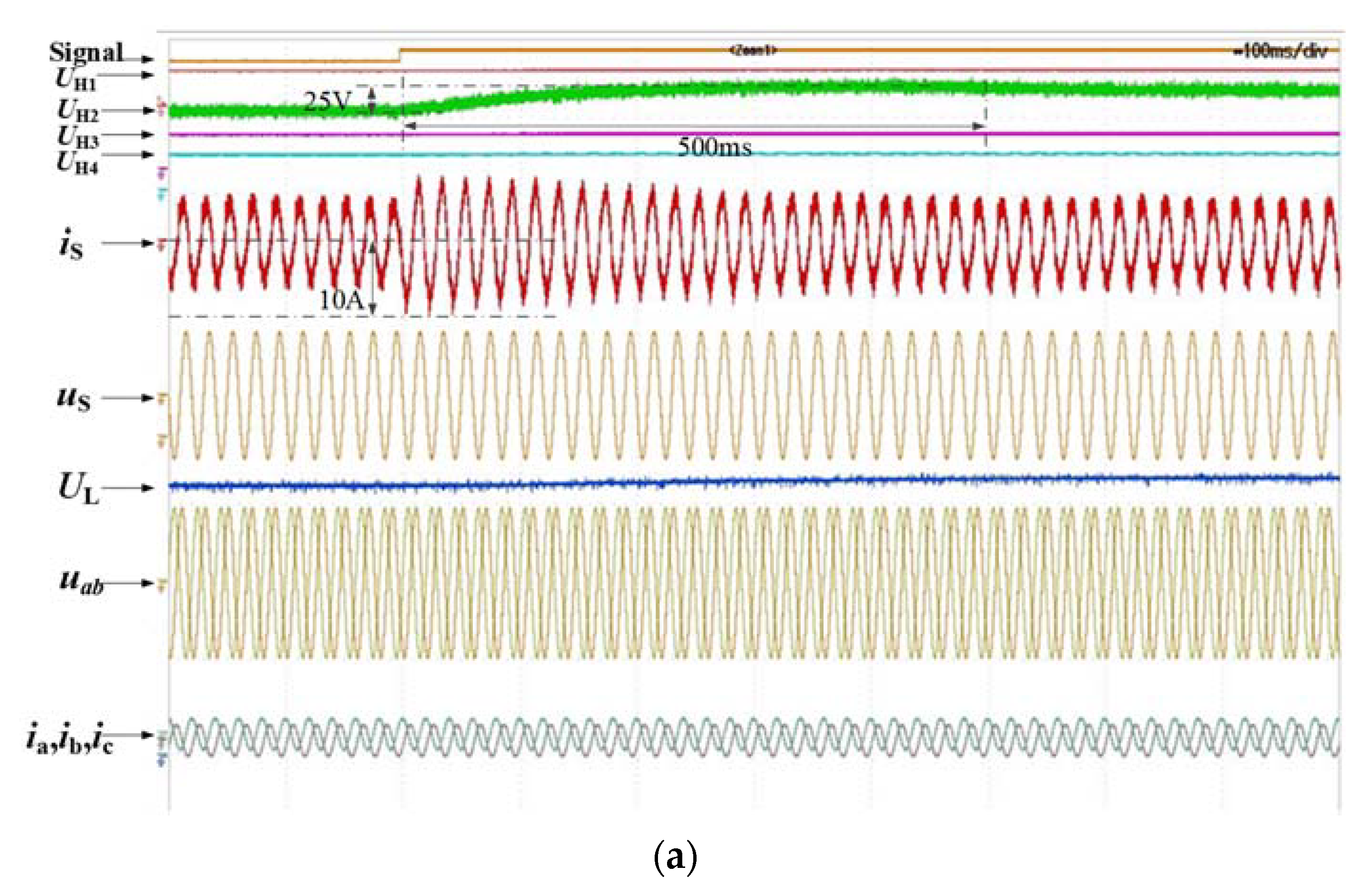
6.2. Experimental Results

The photograph of the experimental prototype is displayed in Figure 21. Considering the load power limitation in the lab, the load power in the experiment changes from 5.20 kW to 9.68 kW, and the other parameters are the same as those used in the simulations.
Figure 22 demonstrates the experimental waveforms of the four CDB voltages (UH4, UH3, UH2, and UH1), the LDB voltage (UL), the input current (is), the input voltage (us), and output ac line voltage (uab), and the output ac currents (ia, ib, and ic) used by the PI controller and the EBC controller, respectively, in the rectifier and the DAB. For displaying clearly the deviation of the CDB voltage during the transient process, the second CDB voltage UH2 is shown in an ac coupling method, and the others are shown in a dc coupling method. With the load power steps, the recovery time of the CDB voltage with the EBC controller is smaller than that in the PI controller, as is shown in Figure 22a,b. The CDB voltage deviation with the EBC controller is similar than that in the PI controller, as is shown in Figure 22b,c. The experiment results have a little difference from the simulation waveforms; the reason is that the changed load power is not obvious for the previous load, and the calculation deviation for the second harmonics voltage ripple has been influenced by measurement error.
The different time scales of the EBC controllers are used in the rectifier and the DAB simultaneously; the transient performance of the two dc bus voltages is more improved than those with the PI controller, as is shown in Figure 22d. The reason is that the interaction between the energy of the CDB capacitors and the LDB capacitors has been considered in the EBC control strategy.
The trajectories of the above four experimental waveforms in the phase plane are shown in Figure 23. The area surrounded by the trajectories obtained by the EBC controller is the smallest, which verifies that EBC has good transient performance. In the figure, the horizontal axis is the voltage of LDB UL, and the vertical axis is the ac coupling value of the 2nd CDB voltage UH2.
The experimental results also verify the control performance of the EBC controller when the CDB voltage reference changes from 680 V to 700 V. Figure 24 demonstrates the experimental waveforms of the signal of the voltage reference changes, the four CDB voltages (UH4, UH3, UH2, and UH1), the LDB voltage (UL), the input current (is), the input voltage (us), and the output ac line voltage (uab); the output ac currents (ia, ib, and ic) used the PI controller and the EBC controller, respectively, in the different current-limited references. In Figure 24a, the current-limited reference is set up to 10 A; the input current rises to 10 A and then decreases slowly for the charging of the dc bus voltages under the PI controller. In Figure 24b, the current-limited reference is also set up to 10 A; the input current rises to 10 A and then keeps within the limited value until the dc bus voltage reaches the reference value. If the current-limited reference can increase further, for example from 10 A to 30 A, the dc bus voltage can realize the faster transient performance in Figure 24c. Therefore, by utilizing the reasonable current-limit value, the EBC controller can achieve a better transient performance than the PI controller.

7. Conclusions

For the voltage-sensitive loads connected with the PET, the EBC strategy can achieve a better transient performance of the dc bus voltages than the conventional PI control strategy. The essential reason is that the interaction between the energy of the CDB capacitors and the LDB capacitors has been considered in the EBC control strategy with different time scales. Through the small-signal analysis of the control strategy in the CDB voltage and LDB voltage, the EBC control strategy can eliminate the impacts of the dc bus capacitors and the fluctuations of the load power compared with the PI control scheme. The stability of the EBC strategy is proved by the stability analysis. The expression of the second harmonic in the CDB voltage is deduced through the instantaneous power-balance relationship in the single-phase PET, and it is helpful in improving the transient performance. Combined with the voltage balance control scheme, the proposed EBC strategy can realize the voltage balance in the cascaded modules. The EBC strategy can be extended to PET, which consists of n-H-bridge rectifier modules and n-DAB converter modules. The simulation and the experimental results prove the effectiveness of the proposed control strategy.

Author Contributions

Conceptualization, G.F.; data curation, P.B.; formal analysis, G.F.; methodology, G.F.; project administration, L.Y.; software, P.B.; supervision, L.Y. All authors have read and agreed to the published version of the manuscript.

Funding

This research was funded by the National Key Research and Development Program of China grant number 2020YFB1314002 And The APC was funded by 2020YFB1314002.

Institutional Review Board Statement

Not applicable.

Informed Consent Statement

Not applicable.

Data Availability Statement

The data presented in this study are available on request from the corresponding author.

Conflicts of Interest

The authors declare that there are no conflicts of interest regarding the publication of this paper.

References

  1. Mishra, D.K.; Ghadi, M.J.; Li, L.; Hossain, M.J.; Zhang, J.; Ray, P.K.; Mohanty, A. A review on solid-state transformer: A breakthrough technology for future smart distribution grids. Int. J. Electr. Power Energy Syst. 2021, 133, 107255. [Google Scholar] [CrossRef]
  2. Chen, M.; Chou, S.-F.; Blaabjerg, F.; Davari, P. Overview of Power Electronic Converter Topologies Enabling Large-Scale Hydrogen Production via Water Electrolysis. Appl. Sci. 2022, 12, 1906. [Google Scholar] [CrossRef]
  3. Sha, G.L.; Duan, Q.; Sheng, W.X.; Pan, A.Q.; Zheng, Y. A Multiport Electric Energy Routing Scheme Applied to Battery Energy Storage System. J. Eng. 2021, 2021, 6637926. [Google Scholar] [CrossRef]
  4. Zheng, L.; Kandula, R.P.; Divan, D. Current-Source Solid-State DC Transformer Integrating LVDC Microgrid, Energy Storage, and Renewable Energy Into MVDC Grid. IEEE Trans. Power Electron. 2022, 37, 1044–1058. [Google Scholar] [CrossRef]
  5. Wang, D.; Guan, Z.; Tian, J.; Mao, C.X.; Yang, Y.; Wang, Z. A hybrid redundancy scheme for medium-voltage three-phase cascaded H-bridge electronic power transformer. IET Power Electron. 2022, 1–14. [Google Scholar] [CrossRef]
  6. Xu, X.; Huang, W.; Hu, Y.; Tai, N.; Ji, Y.; Xie, N. Power Management of AC/DC Hybrid Distribution Network With Multi-Port PET Considering Reliability of Power Supply System. Front. Energy Res. 2021, 9, 721385. [Google Scholar] [CrossRef]
  7. Li, K.; Wen, W.; Zhao, Z.; Yuan, L.; Cai, W.; Mo, X.; Gao, C. Design and Implementation of Four-Port Megawatt-Level High-Frequency-Bus Based Power Electronic Transformer. IEEE Trans. Power Electron. 2021, 36, 915–927. [Google Scholar] [CrossRef]
  8. Teng, J.; Sun, X.; Zhang, Y.; Fu, H.; Liu, X.; Zhao, W.; Li, X. Two Types of Common-Mode Voltage Suppression in Medium Voltage Motor Speed Regulation System Based on Solid State Transformer With Dual DC Bus. IEEE Trans. Power Electron. 2022, 37, 7082–7099. [Google Scholar] [CrossRef]
  9. Nair, A.C.; Fernandes, B.G. A Solid State Transformer based Fast Charging Station for Various Categories of Electric Vehicles with Batteries of Vastly Different Ratings. IEEE Trans. Ind. Electron. 2022, in press. [Google Scholar] [CrossRef]
  10. Perez, M.A.; Bernet, S.; Rodriguez, J.; Kouro, S.; Lizana, R. Circuit Topologies, Modeling, Control Schemes, and Applications of Modular Multilevel Converters. IEEE Trans. Power Electron. 2015, 30, 4–17. [Google Scholar] [CrossRef]
  11. Liu, W.; Zhang, K.; Chen, X.; Xiong, J. Simplified model and submodule capacitor voltage balancing of single-phase AC/AC modular multilevel converter for railway traction purpose. IET Power Electron. 2016, 9, 951–959. [Google Scholar] [CrossRef] [Green Version]
  12. Ma, D.; Lin, S.; Cheng, Q.; Sun, Q. The DC Bus Voltage Control Based on Virtual Inertia for SST. In Proceedings of the 2018 IEEE 7th Data Driven Control and Learning Systems Conference (DDCLS), Enshi, China, 25–27 May 2018; pp. 575–580. [Google Scholar]
  13. Zhao, T.; She, X.; Bhattacharya, S.; Wang, G.; Wang, F.; Huang, A. Power synchronization control for capacitor minimization in Solid State Transformers (PET). In Proceedings of the 2011 IEEE Energy Conversion Congress and Exposition, Phoenix, AZ, USA, 17–22 September 2011; pp. 2812–2818. [Google Scholar]
  14. Wang, G.; She, X.; Wang, F.; Kadavelugu, A.; Zhao, T.; Huang, A.; Yao, W. Comparisons of different control strategies for 20 kVA solid state transformer. In Proceedings of the 2011 IEEE Energy Conversion Congress and Exposition, Phoenix, AZ, USA, 17–22 September 2011; pp. 3173–3178. [Google Scholar]
  15. Zheng, L.; Kandula, R.P.; Kandula, R.P.; Divan, D. New Modulation and Impact of Transformer Leakage Inductance on Current-Source Solid-State Transformer. IEEE Trans. Power Electron. 2022, 37, 562–576. [Google Scholar] [CrossRef]
  16. Liu, Y.; Yang, S.; Zhang, S.; Peng, F.Z. Comparison of Synchronous Condenser and STATCOM for Inertial Response Support. In Proceedings of the 2014 IEEE Energy Conversion Congress and Exposition (ECCE), Pittsburgh, PA, USA, 14–18 September 2014; pp. 2684–2690. [Google Scholar]
  17. He, F.; Zhao, Z.; Yuan, L.; Lu, S. A DC-link voltage control scheme for single-phase grid-connected PV inverters. In Proceedings of the 2011 IEEE Energy Conversion Congress and Exposition, Phoenix, AZ, USA, 17–22 September 2011; pp. 3941–3945. [Google Scholar]
  18. Ge, J.; Zhao, Z.; Yuan, L.; Lu, T. Energy Feed-Forward and Direct Feed-Forward Control for Solid-State Transformer. IEEE Trans. Power Electron. 2015, 30, 4042–4047. [Google Scholar] [CrossRef]
  19. Dash, S.K.; Ray, P.K. A New PV-Open-UPQC Configuration for Voltage Sensitive Loads utilizing novel Adaptive Controllers. IEEE Trans. Ind. Electron. 2022, in press. [Google Scholar] [CrossRef]
  20. Bahraini, F.; Abrishamifar, A.; Ayatollahi, A. Fast DC Bus Voltage Regulation for a Low Cost Single-Phase Grid-Connected PV Microinverter With a Small DC Bus Capacitor. In Proceedings of the 2020 11th Power Electronics, Drive Systems, and Technologies Conference (PEDSTC), Tehran, Iran, 4–6 February 2020. [Google Scholar]
  21. Alemi, P.; Bae, C.J.; Lee, D.C. Resonance Suppression Based on PR Control for Single-Phase Grid-Connected Inverters with LLCL Filters. IEEE J. Emerg. Sel. Top. Power Electron. 2016, 4, 459–467. [Google Scholar] [CrossRef]
  22. Gao, Y.G.; Jiang, F.Y.; Song, J.C.; Zheng, L.J.; Tian, F.Y.; Geng, P.L. A novel dual closed-loop control scheme based on repetitive control for grid-connected inverters with an LCL filter. ISA Trans. 2018, 74, 194–208. [Google Scholar] [CrossRef] [PubMed]
  23. Ouyang, H.; Zhang, K.; Zhang, P.; Kang, Y.; Xiong, J. Repetitive Compensation of Fluctuating DC Link Voltage for Railway Traction Drives. IEEE Trans. Power Electron. 2011, 26, 2160–2171. [Google Scholar] [CrossRef]
  24. Wang, R.; Wang, F.; Boroyevich, D.; Burgos, R.; Lai, R.; Ning, P.; Rajashekara, K. A High Power Density Single-Phase PWM Rectifier With Active Ripple Energy Storage. IEEE Trans. Power Electron. 2011, 26, 1430–1443. [Google Scholar] [CrossRef]
Figure 1. The contents of each section and their relationship.
Energies 15 03129 g001
Figure 2. The single-phase PET: (a) structure, (b) instantaneous power relationship in PET, (c) energy relationship in PET.
Energies 15 03129 g002
Figure 3. The average model of the single-phase PET.
Energies 15 03129 g003
Figure 4. EBC Control model for the LDB voltage.
Energies 15 03129 g004
Figure 5. Small-signal model for the LDB voltage based on EBC controller.
Energies 15 03129 g005
Figure 6. Small-signal model for the LDB voltage based on PI controller.
Energies 15 03129 g006
Figure 7. Pole distribution of the LDB voltage control system based on EBC controller.
Energies 15 03129 g007
Figure 8. EBC control model for the CDB voltage.
Energies 15 03129 g008
Figure 9. Simplified EBC control model for the CDB voltage.
Energies 15 03129 g009
Figure 10. Small-signal model for the CDB voltage based on EBC controller.
Energies 15 03129 g010
Figure 11. Small-signal model for the CDB voltage based on PI controller.
Energies 15 03129 g011
Figure 12. Pole distribution of the CDB voltage control system based on EBC controller.
Energies 15 03129 g012
Figure 13. Influence of capacitance and inductance deviation on bus voltage: (a) ±30% same-direction deviation in two-stage bus capacitance, (b) ±30% reverse-direction deviation in two-stage bus capacitance, (c) ±30% deviation in the grid side inductance.
Energies 15 03129 g013aEnergies 15 03129 g013b
Figure 14. Control scheme in the parallel DABs.
Energies 15 03129 g014
Figure 15. Proposed EBC strategy for PET.
Energies 15 03129 g015
Figure 16. Comparison of the four CDB voltages for the load power steps (from 1.4 kW to 28 kW).
Energies 15 03129 g016
Figure 17. Comparison of the CDB voltage and the LDB voltage for load power steps (from 1.4 kW to 28 kW): (a) with PI controller in CDB voltage and LDB voltage, (b) with EBC controller in CDB voltage and with PI controller in LDB voltage, (c) with PI controller in CDB voltage and with EBC controller in LDB voltage, (d) with EBC controller in CDB voltage and LDB voltage.
Energies 15 03129 g017aEnergies 15 03129 g017b
Figure 18. Phase-plan diagrams of the average of the CDB voltage and the LDB voltage: (a) With PI controller in CDB voltage and LDB voltage, (b) with EBC controller in CDB voltage and with PI controller in LDB voltage, (c) with PI controller in CDB voltage and with EBC controller in LDB voltage, (d) with EBC controller in CDB voltage and LDB voltage.
Energies 15 03129 g018
Figure 19. Comparison of the four CDB voltages for voltage reference rises (from 680 to 700 V).
Energies 15 03129 g019
Figure 20. Four CDB voltages and parallel transmitted power waveforms: (a) without voltage balance control, (b) with voltage balance control using PI controller, (c) with voltage balance control using EBC controller.
Energies 15 03129 g020
Figure 21. Photograph of the prototype.
Energies 15 03129 g021
Figure 22. The transient experiment waveforms for load power steps (from 5.20 kW to 9.68 kW) (from top to bottom: UH4 (500 V/div), UH3 (500 V/div), UH2 (2 V/div, ac coupling), UH1 (500 V/div), UL (200 V/div), is (5 A/div), us (1 kV/div), uab (400 V/div), iabc (20 A/div)): (a) with the PI controller in the CDB and LDB voltage, (b) with the EBC controller in the CDB voltage, with the PI controller in the LDB voltage, (c) with the PI controller in the CDB voltage, with the EBC controller in the LDB voltage, (d) with the EBC controller in the CDB and LDB voltage.
Energies 15 03129 g022aEnergies 15 03129 g022b
Figure 23. Phase-plane diagrams of the average of the CDB voltage and the LDB voltage: (a) with the PI controller in the CDB and LDB voltage, (b) with the EBC controller in the CDB voltage, with the PI controller in the LDB voltage, (c) with the PI controller in the CDB voltage, with the EBC controller in the LDB voltage, (d) with the EBC controller in the CDB and LDB voltage.
Energies 15 03129 g023aEnergies 15 03129 g023b
Figure 24. The transient experiment waveforms for voltage reference rises (from 680 to 700 V) (from top to bottom: the signal for the voltage reference changes, UH1 (500 V/div), UH2 (25 V/div), UH3 (500 V/div), UH4 (500 V/div), is (5 A/div), us (1 kV/div), UL (200 V/div), uab (400 V/div), iabc (20 A/div)): (a) with the PI controller in current-limited reference, (b) with the EBC controller in current-limited reference, (c) with the EBC controller in increased current-limited reference.
Energies 15 03129 g024aEnergies 15 03129 g024b
Table 1. Parameters of Simulation Circuit.
ParametersValuesParametersValues
Input ac voltage us1732 VCDB capacitor CH4700 uF
CDB voltage UH700 VLDB capacitor CL19,000 uF
LDB voltage UL700 VTransformer turns ratio n1:1
Input inductor Ls5 mHHFT leakage inductor Ls328 uH
Publisher’s Note: MDPI stays neutral with regard to jurisdictional claims in published maps and institutional affiliations.

