

Impact of Air Gap Defects on the Electrical and Mechanical Properties of a 320 kV Direct Current Gas Insulated Transmission Line Spacer

 ,
,
Abstract
:1. Introduction
2. Simulation Model
2.1. Geometry
2.2. Equation Derivation and Boundary Conditions
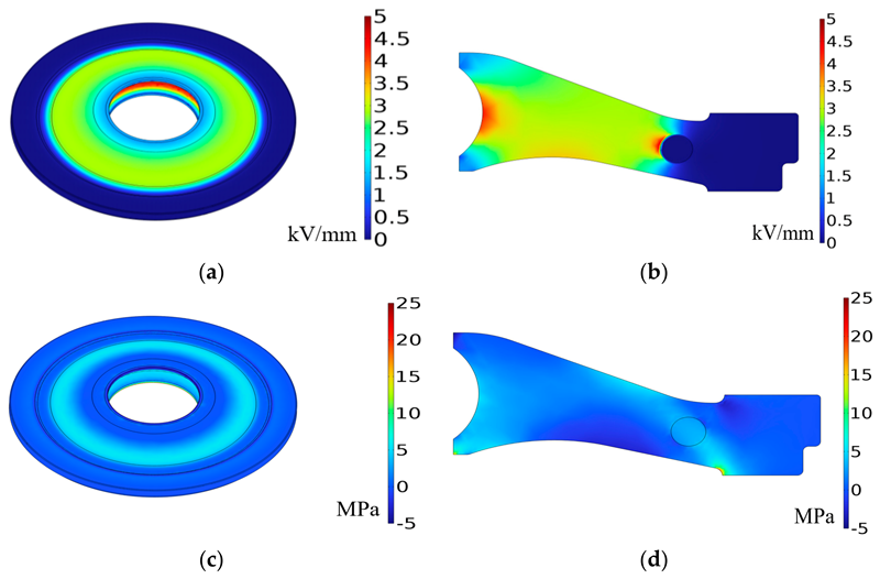
2.3. Performance Analysis with a Defect-Free Model
3. Impact on Model Performance of a Radially Distributed Air Gap Defect
3.1. Arrangement of the Air Gap Defect along the Radial Direction of the Insulation Spacer
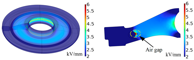
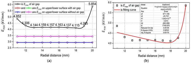
3.2. Impact on Electric Field Distribution
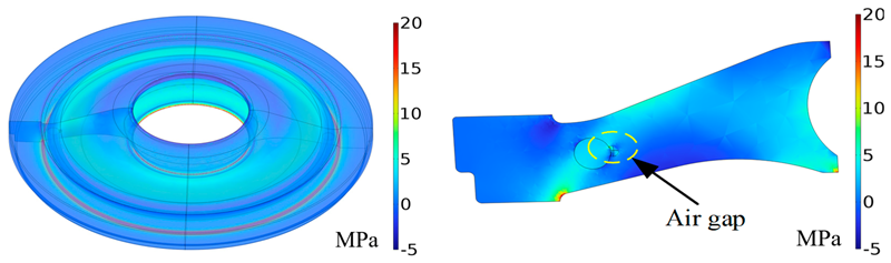
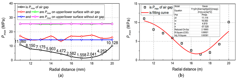
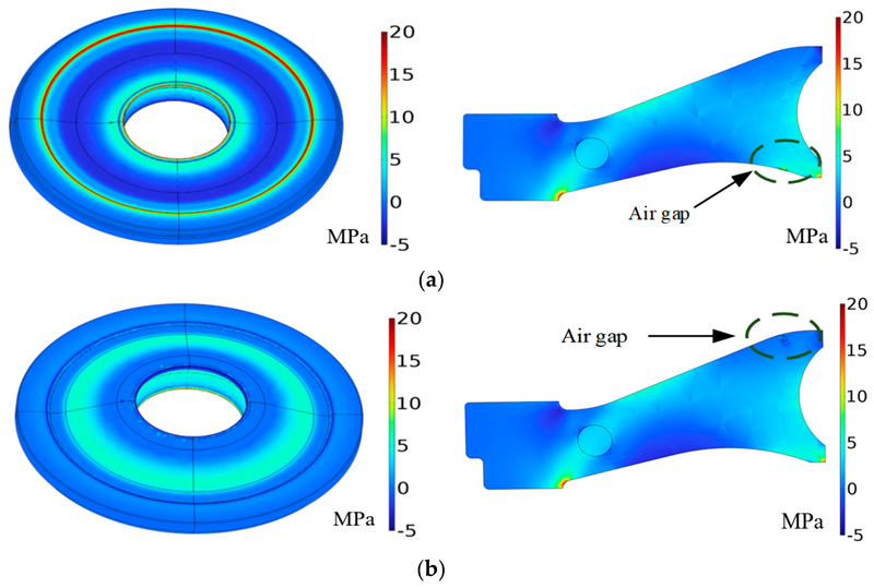
3.3. Impact on Mechanical Stress Distribution
4. Impact on Model Performance under an Axially Distributed Air Gap Defect
4.1. Arrangement of an Air Gap Defect along the Axial Direction of the Insulation Spacer
4.2. Impact on Electric Field Distribution
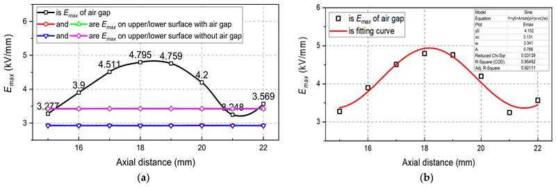
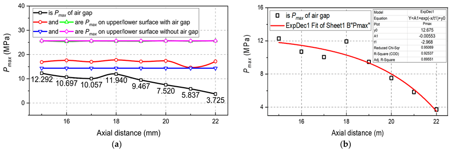
4.3. Impact on Mechanical Stress Distribution
5. Conclusions
Author Contributions
Funding
Data Availability Statement
Conflicts of Interest
References
- Li, C.; Zhang, C.; Lv, J.; Liang, F.; Liang, Z.; Fan, X.; Riechert, U.; Li, Z.; Liu, P.; Xue, J.; et al. China’s 10-year progress in DC gas-insulated equipment: From basic research to industry perspective. Ienergy 2022, 1, 400–433. [Google Scholar] [CrossRef]
- Fan, X.H.; Liu, J.F.; Goh, H.W.; Zhang, Y.; Wu, T.; Liu, J. Aging Analysis of Transformer Insulation at Weakest Region: Dielectric Parameters Extraction via Immune Optimization. IEEE Trans. Transp. Electrif. 2022, 9, 1579–1589. [Google Scholar] [CrossRef]
- Fan, X.H.; Liu, J.F.; Goh, H.W.; Zhang, Y.; Zhang, G.; Rahman, S. Acquisition of FDS for Oil-Immersed Insulation at Transformer Hotspot Region Based on Multiconstraint NSGA Model. IEEE Trans. Ind. Electrons. 2022, 69, 13625–13635. [Google Scholar] [CrossRef]
- Li, C.; Yang, Y.; Xu, G.; Zhou, Y.; Jia, M.; Zhong, S.; Gao, Y.; Park, C.; Liu, Q.; Wang, Y.; et al. Insulating materials for realising carbon neutrality: Opportunities, remaining issues and challenges. High Volt. 2022, 7, 610–632. [Google Scholar] [CrossRef]
- Jia, C.; Zhao, W.; Zhu, Y.; Lu, W.; Tang, Z. A Numerical Study on the Decomposition and Diffusion Characteristics of SF6 in Gas-Insulated Switchgear with Consideration of the Temperature Rising Effect. Energies 2022, 15, 7834. [Google Scholar] [CrossRef]
- Rachmawati; Kojima, H.; Kato, K.; Zebouchi, N.; Hayakawa, N. Electric Field Grading and Discharge Inception Voltage Improvement on HVDC GIS/GIL Spacer with Permittivity and Conductivity Graded Materials (ε/σ-FGM). IEEE Trans. Dielectr. Electr. Insul. 2022, 29, 1811–1817. [Google Scholar] [CrossRef]
- Du, B.X.; Dong, J.N.; Liang, H.C. Electric field control by permittivity functionally graded and superficially non-linear conductivity materials for DC-GIS spacer. High Volt. 2022, 7, 992–1000. [Google Scholar] [CrossRef]
- Zhao, C.; Tang, Z.; Zhang, L.; Wu, D.; Xia, H.; Li, H.; Pan, K. Entire process of surface discharge of GIS disc-spacers under constant AC voltage. High Volt. 2020, 5, 591–597. [Google Scholar] [CrossRef]
- Yang, D.; Tang, J.; Zeng, F.; Yang, X.; Yao, Q.; Miao, Y.; Chen, L. Correlation characteristics between SF6 decomposition process and partial discharge quantity under negative DC condition initiated by free metal particle defect. IEEE Trans. Dielectr. Electr. Insul. 2018, 25, 574–583. [Google Scholar] [CrossRef]
- Lu, L.; Ichimura, S.; Rokunohe, T. Interaction Between Partial Discharge and Generated Bubbles Under Repeated Lightning Impulses in Transformers Using a Complex Structure Model. IEEE Trans. Dielectr. Electr. Insul. 2021, 28, 727–735. [Google Scholar] [CrossRef]
- Yadam, Y.R.; Sarathi, R.; Arunachalam, K. Numerical and Experimental Investigations on Influence of Internal Defect Parameters on Partial Discharge Induced UHF Signals in Gas Insulated Switchgear. IEEE Access 2022, 10, 110785–110795. [Google Scholar] [CrossRef]
- Shiling, Z. Relationship between Electric Field Distribution Computation and Insulation Performance of GIS Spacer. In Proceedings of the 2020 IEEE 6th International Conference on Computer and Communications (ICCC), Chengdu, China, 11–14 December 2020; pp. 2397–2402. [Google Scholar]
- Li, X.; Liu, W.; Xu, Y.; Ding, D. Discharge Characteristics and Detectability of Metal Particles on the Spacer Surface in Gas-Insulated Switchgears. IEEE Trans. Power Del. 2022, 37, 187–196. [Google Scholar] [CrossRef]
- Wang, W.; Gao, Y.; Zhao, H. The Effect of a Metal Particle on Surface Charge Accumulation Behavior of Epoxy Insulator with Zoning Coating. Energies 2022, 15, 4730. [Google Scholar] [CrossRef]
- Cho, H.G.; Hong, Y.-G.; Noh, Y.-H.; Bae, J.; Lee, J. Effect of Bio-based Epoxy Resins on the Thermal, Mechanical Properties and their Applicability to Gas Insulated Switchgear Spacer Materials. In Proceedings of the 2022 6th International Conference on Electric Power Equipment-Switching Technology (ICEPE-ST), Seoul, Republic of Korea, 15–18 March 2022; pp. 271–274. [Google Scholar]
- Chen, T.; Shafai, C.; Rajapakse, A.; Liyanage, J.; Neusitzer, T. Micromachined AC/DC electric field sensor with modulated sensitivity. Sens. Actuator A Phys. 2016, 245, 76–84. [Google Scholar] [CrossRef]
- Li, Z.; Yuan, H.; Cui, Y.; Ding, Z.; Zhao, L. Measurement of distorted power-frequency electric field with integrated optical sensor. IEEE Trans. Instrum. Meas. 2019, 68, 1132–1139. [Google Scholar] [CrossRef]
- Ji, S.; Jia, Y.; Yang, X.; Liu, Z.; Zhu, L. A Method for Measuring Electric Field Distribution along Insulator Surfaces Based on Electroluminescence Effect and Its Image Processing Algorithm. IEEE Trans. Dielectr. Electr. Insul. 2022, 29, 939–947. [Google Scholar] [CrossRef]
- Moradnouri, A.; Vakilian, M.; Hekmati, A.; Fardmanesh, M. The End Part of cryogenic HV Bushing Insulation Design in a 230/20 kV HTS Transformer. Cryogenics 2020, 108, 103090. [Google Scholar] [CrossRef]
- Ji, S.; Jia, Y.; Yang, X.; Liu, Z.; Zhu, L. Simulation and experimental study on mechanical performance of UHV GIS spacer in hydrostatic test. IEEE Trans. Dielectr. Electr. Insul. 2017, 24, 3122–3313. [Google Scholar]
- Wang, Q.; Fan, X.; Ding, Z.; Hwang, G.H.; Zhang, Y.; Liu, J. A Genetic Optimization Model for Aging Analysis of Paper Insulation in High-Temperature Region via Frequency Domain Spectroscopy. IEEE Trans. Transport. Electrific. 2022. [Google Scholar] [CrossRef]
- Talaat, M.; El-Zein, A.; Amin, M. Electric field simulation for uniform and FGM cone type spacer with adhering spherical conducting particle in GIS. IEEE Trans. Dielectr. Electr. Insul. 2018, 25, 339–351. [Google Scholar] [CrossRef]
- Wang, H.; Peng, Z.; Guo, Z.; Wang, Q.; Liao, J.; Zhang, S. Simulation study of electric influence caused by defects on UHV AC GIS spacer. In Proceedings of the 2015 IEEE 11th International Conference on the Properties and Applications of Dielectric Materials (ICPADM), Sydney, NSW, Australia, 19–22 July 2015; pp. 676–679. [Google Scholar]
- Moradnouri, A.; Vakilian, N.; Hekmati, A.; Fardmanesh, M. HTS Transformer’s Partial Discharges Raised by Floating Particles and Nitrogen Bubbles. J. Supercond. Nov. Magn. 2020, 33, 3027–3034. [Google Scholar] [CrossRef]
- Liang, Z.; Lin, C.; Liang, F.; Zhuang, W.; Xu, Y.; Tang, L.; Zeng, Y.; Hu, J.; Zhang, B.; Li, C.; et al. Designing HVDC GIS/GIL spacer to suppress charge accumulation. High Volt. 2022, 7, 645–651. [Google Scholar] [CrossRef]
- Li, X.; Wan, M.; Zhang, G.; Lin, X. Surface Charge Characteristics of DC-GIL Insulator under Multiphysics Coupled Field: Effects of Ambient Temperature, Load Current, and Gas Pressure. IEEE Trans. Dielectr. Electr. Insul. 2022, 29, 1530–1539. [Google Scholar] [CrossRef]


| No. | Component | Geometry Parameter | Material | Material Parameter |
|---|---|---|---|---|
| 1 | Metal shell | Length: 52 cm Radius: 33 cm | Aluminum alloy | Relative permittivity: 1 × 10⁷ Young modulus: 71 GPa Poisson’s ratio: 0.33 Density: 2700 kg/m3 |
| 2 | Center conductor | Length: 52 cm Radius: 9.8 cm | ||
| 3 | Ground ring | Radius: 1 cm | ||
| 4 | Insulation spacer | Max thickness: 5 cm Radius: 27 cm | Epoxy resin | Relative permittivity: 4.95 Young modulus: 13 Gpa Poisson’s ratio: 0.36 Density: 2300 kg/m3 |
| 5 | Air gap | Radius: 0.15 cm | Air | Relative permittivity: 1 |
| Items | Emax (kV/mm) | Pmax (MPa) |
|---|---|---|
| Upper surface | 2.929 | 14.365 |
| Lower surface | 3.427 | 25.632 |
| X-dis | 11 mm | 12 mm | 13 mm | 14 mm | 15 mm |
| Emax | 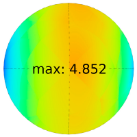 |  | 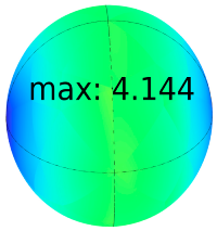 | 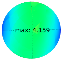 | 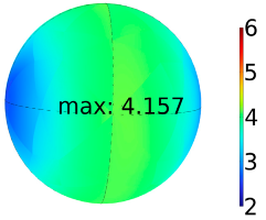 |
| X-dis | 16 mm | 17 mm | 18 mm | 19 mm | 20 mm |
| Emax | 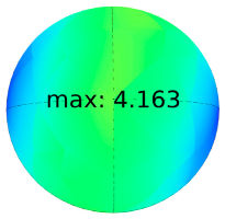 | 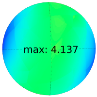 | 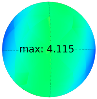 | 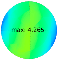 |  |
| X-dis | 11 mm | 12 mm | 13 mm | 14 mm | 15 mm |
| ke_upper | 1.657 | 1.470 | 1.415 | 1.420 | 1.419 |
| ke_lower | 1.416 | 1.257 | 1.209 | 1.214 | 1.213 |
| X-dis | 16 mm | 17 mm | 18 mm | 19 mm | 20 mm |
| ke_upper | 1.421 | 1.412 | 1.405 | 1.456 | 1.999 |
| ke_lower | 1.215 | 1.207 | 1.201 | 1.244 | 1.708 |
| X-dis | 11 mm | 12 mm | 13 mm | 14 mm | 15 mm |
| Pmax |  |  | 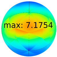 | 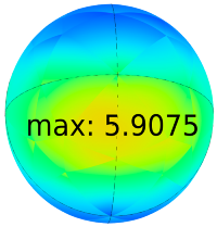 | 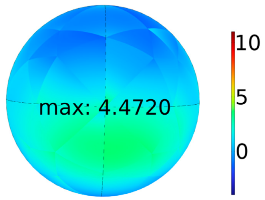 |
| X-dis | 16 mm | 17 mm | 18 mm | 19 mm | 20 mm |
| Pmax |  | 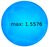 | 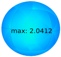 | 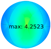 |  |
| X-dis | 11 mm | 12 mm | 13 mm | 14 mm | 15 mm |
| ke_upper | 0.770 | 0.567 | 0.499 | 0.411 | 0.311 |
| ke_lower | 0.431 | 0.318 | 0.280 | 0.230 | 0.174 |
| X-dis | 16 mm | 17 mm | 18 mm | 19 mm | 20 mm |
| ke_upper | 0.180 | 0.108 | 0.142 | 0.296 | 0.705 |
| ke_lower | 0.101 | 0.061 | 0.080 | 0.166 | 0.395 |
| X-dis | 15 mm | 16 mm | 17 mm | 18 mm |
| Emax |  |  |  |  |
| X-dis | 19 mm | 20 mm | 21 mm | 22 mm |
| Emax |  |  |  |  |
| X-dis | 15 mm | 16 mm | 17 mm | 18 mm |
| ke_upper | 1.117 | 1.332 | 1.541 | 1.641 |
| ke_lower | 0.959 | 1.141 | 1.314 | 1.397 |
| X-dis | 19 mm | 20 mm | 21 mm | 22 mm |
| ke_upper | 1.626 | 1.431 | 1.109 | 1.220 |
| ke_lower | 1.386 | 1.229 | 0.950 | 1.044 |
| X-dis | 15 mm | 16 mm | 17 mm | 18 mm |
| Pmax |  | 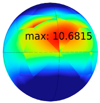 | 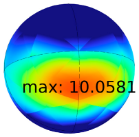 | 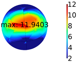 |
| X-dis | 19 mm | 20 mm | 21 mm | 22 mm |
| Pmax | 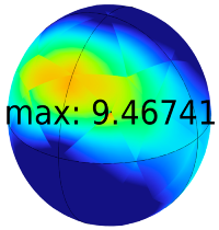 | 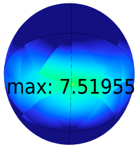 | 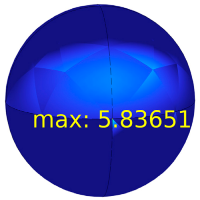 | 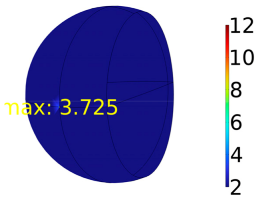 |
| X-dis | 15 mm | 16 mm | 17 mm | 18 mm |
| ke_upper | 0.729 | 0.608 | 0.592 | 0.672 |
| ke_lower | 0.479 | 0.421 | 0.393 | 0.468 |
| X-dis | 19 mm | 20 mm | 21 mm | 22 mm |
| ke_upper | 0.553 | 0.432 | 0.399 | 0.217 |
| ke_lower | 0.371 | 0.293 | 0.229 | 0.145 |
Disclaimer/Publisher’s Note: The statements, opinions and data contained in all publications are solely those of the individual author(s) and contributor(s) and not of MDPI and/or the editor(s). MDPI and/or the editor(s) disclaim responsibility for any injury to people or property resulting from any ideas, methods, instructions or products referred to in the content. |
© 2023 by the authors. Licensee MDPI, Basel, Switzerland. This article is an open access article distributed under the terms and conditions of the Creative Commons Attribution (CC BY) license (https://creativecommons.org/licenses/by/4.0/).
Share and Cite
Deng, Y.; Fan, X.; Luo, H.; Wang, Y.; Wu, K.; Liang, F.; Li, C. Impact of Air Gap Defects on the Electrical and Mechanical Properties of a 320 kV Direct Current Gas Insulated Transmission Line Spacer. Energies 2023, 16, 4006. https://doi.org/10.3390/en16104006
Deng Y, Fan X, Luo H, Wang Y, Wu K, Liang F, Li C. Impact of Air Gap Defects on the Electrical and Mechanical Properties of a 320 kV Direct Current Gas Insulated Transmission Line Spacer. Energies. 2023; 16(10):4006. https://doi.org/10.3390/en16104006
Chicago/Turabian StyleDeng, Yuan, Xianhao Fan, Hanhua Luo, Yao Wang, Keyan Wu, Fangwei Liang, and Chuanyang Li. 2023. "Impact of Air Gap Defects on the Electrical and Mechanical Properties of a 320 kV Direct Current Gas Insulated Transmission Line Spacer" Energies 16, no. 10: 4006. https://doi.org/10.3390/en16104006