Abstract
Solar energy is the most used renewable energy source. CZTSSe uses earth-abundant elements and has promising optoelectronic properties, resulting in becoming a viable alternative to thin film PV. This work provides design guidelines for CZTSSe-based solar cells, where CZTSSe has a tunable affinity and energy gap. The analysis is based on incorporating a ternary compound material to serve as an electron transport material (ETM). In this regard, CdZnS is a potential candidate that can be utilized as an electron transport layer whose affinity and energy gap can be tuned to adjust the band alignment at the ETL/CZTSSe interface. In order to design a high-efficiency solar cell, one has to tune both the ETL and absorber layers to have a suitable conduction band offset (CBO), thereby minimizing the non-radiative recombination which, in turn, boosts the power conversion efficiency (PCE). Thus, in our presented simulation study, we provide a codesign of alloy compositions of both the CZTSSe photoactive layer and the CdZnS ETL using SCAPS-1D simulation. It is found that using the codesign of alloy compositions of the ternary compound ETL and the absorber enhances the PCE by about 2% and, more importantly, overcomes the main issue in CZTSSe which is its open-circuit voltage (VOC) deficit. Furthermore, upon optimizing the thickness and doping of both the ETL and absorber layer, as well as the bulk defect of the absorber layer, a PCE of 17.16% is attained in this study, while the calibrated PCE based on a previously published experimental work was 12.30%.
1. Introduction
To address the challenges posed by climate change, it is imperative to focus on the development of renewable energy sources, particularly solar photovoltaic (PV) energy [1]. PV energy has the capacity to transform an unlimited supply of sunlight into electrical energy. Many efforts have been established to achieve high power-conversion efficiency (PCE) PV cells with lower costs including silicon and other thin film materials [2,3,4,5,6,7,8]. Thin film solar cells are a type of PV cell that are made by depositing extremely thin layers of PV materials onto a substrate. These materials can be made from a variety of substances, including silicon, copper indium gallium selenide (CIGS), cadmium telluride (CdTe), and organic photovoltaics (OPVs). Thin film solar cells are a promising technology for generating clean, renewable energy. They offer several advantages over traditional silicon solar cells, including lower material costs, lighter weight, and greater flexibility. In addition, they can be produced using less energy than silicon solar cells, making them more environmentally friendly. Despite their potential benefits, thin film solar cells are still a relatively new technology and are not yet widely used on a large scale. However, ongoing research and development efforts are focused on improving the efficiency and durability of these cells, which could help make them a viable alternative to traditional solar cells in the future. Of the many thin-film materials used in solar cell fabrication that have been developed for use in low-processing cost solar cells, Cu2ZnSn(SxSe1-x)4 (CZTSSe) has drawn substantial concern from the perspective of PV technologies. CZTSSe utilizes Earth-abundant and non-toxic elements and has beneficial band gap energies (Eg) in the range 1.0–1.5 eV besides their high absorption coefficients (>104 cm−3), in addition to its p-type conductivity nature [9,10,11].
However, compared with Si, CdTe, and CIGS, the PCE of CZTSSe still has lower records. Experimental studies report efficiencies of 12.70% with double emitters produced by solution techniques [12] and 12.30% [13] fabricated via sputtering deposition procedures. Meanwhile, the theoretically limiting efficiency is about 32.80% [14]. The low efficiency can be ascribed to the larger open circuit voltage (VOC) deficit. This deficit can result from recombination losses at the p-n heterojunction interface, an improper choice of the conduction band offset (CBO) between the photoactive layer and the electron transport layer (ETL), un-passivated interface defects, and/or low carrier lifetimes [11,15,16,17,18]. There are a lot of both experimental and theoretical efforts that have been undertaken to push the PCE of CZTSSe by mainly reducing the VOC deficit [19,20,21,22,23]. In this regard, Yan et al. reported a technique of utilizing two thin films that have distinctive doping levels [19]. Kim et al. presented an experimental study in which they achieved passivation of both front and back interfaces, thereby reducing the recombination, which results in enhancing the PCE [20]. By substituting Ag, which has a relatively large atomic radius, into the host CZTSSe by utilizing aqueous spray pyrolysis, an efficiency of 11.83% was achieved [21]. Further, in [22], the authors managed to control and adjust the ionic movement of Na+, which is incorporated to passivate trap states, and they addressed an improved performance of the fabricated solar cell. Furthermore, to improve the quality of CZTSSe-based cells, sulfurization at reduced temperatures has been investigated, and its useful impact was reflected in a higher PCE of this treatment [23].
The operation of PV cells can be better understood with a numerical analysis, which is also useful for enhancing the efficiency and structure of PV cells. The investigation of the effects of crucial physical parameters, such as the mobility and lifetime of electrons and holes, doping density, affinity, and band gap as well as defects of materials, which are time-consuming processes when being altered experimentally, is made possible by numerical modeling [24,25]. Simulation tools save the effort, time, and money of the researchers. Solar cell devices could be simulated using any numerical program that can resolve the fundamental semiconductor equations. Numerous numerical simulators, including wxAMPS, SILVACO, COMSOL, and SCAPS, have been utilized to investigate the performances of various solar cells, especially thin-film devices. Regarding the simulation efforts applied for CZTSSe-based cells, one can find some useful studies in the literature [11,26,27,28]. In [11], the influence of many key factors, such as the composition ratio, absorber thickness, and defects, as well as temperature have been investigated, and the efficiency has been enhanced where the calibrated cell was based on an experimental work while the simulation analysis was performed using SCAPS software. Further, an investigation of different possible defects has been provided in [26], revealing an optimum PCE of 19.06%. The performance of the CZTSSe solar cell under the influence of different ETLs has been numerically explored [27]. Moreover, a CZTSSe solar cell structure has been proposed and simulated using two different HTLs (Cu2O and MoTe2) [28].
According to previous studies, the significance of the alloy codesign as the sole design of the absorber parameters may not be sufficient to optimize the cell performance. Instead, the ETL should be simultaneously designed with the absorber to meet both a superior absorption and the band alignment at the same time. Regarding CZTSSe-based solar cells, the band alignment issue between the CZTSSe and the ETL layers has not been thoroughly investigated, especially for different compositions of the CZTSSe absorber layer. In addition, tunable electron affinity ETL candidates have not been investigated with CZTSSe. Consequently, in this work, the ETL is simultaneously codesigned with the absorber by tuning the elemental compositions of both the ETL and absorber compounds to achieve the optimum band alignment between them, thereby achieving higher PCEs.
In this work, we provide a proposed solar cell that is based on the device configuration ZnO:Al/i-ZnO/CdZnS/CZTSSe/Mo, where CdZnS serves as an ETL, while Mo serves as an HTL. First, we calibrate this modeling methodology implemented in the simulator versus the experimental structure whose ETL is CdS [29]. Then, the alloy composition codesign concept is applied to improve the efficiency of the cell. In the presented methodology, the electron affinity and energy bandgap of the Cu2ZnSn(SxSe1-x)4 absorber can be engineered by controlling the relative composition (x) of S (and thus Se). On the other hand, the electron affinity and the bandgap of the compound ETL (CdyZn1-yS) are controlled via tuning the composition (y). After obtaining the optimum x and y compositions that achieve the maximum PCE, some steps are conducted to optimize the main device parameters. The impacts of the ETL’s thickness and doping are analyzed to assess their influence on cell performance, followed by an optimization of the ETL’s thickness and doping concentration. The thickness and doping concentration of the absorber layer are then optimized. In addition, the bulk defect density inside the photoactive absorber is investigated. The rest of this paper is organized as follows: Section 2 presents the used materials, methods, and simulation techniques; Section 3 discusses the results; finally, Section 4 concludes the work of this paper.
2. Materials and Methods
2.1. Device Structure and Material Parameters
The arrangement of the investigated CZTSSe solar cell is comprised of a 600 nm thick Mo layer as a rear contact, a 1.8 μm thick CZTSSe thin film, a 50 nm thick CdS buffer ETL, a 50 nm thick intrinsic ZnO layer, a 300 nm thick Al doped ZnO (AZO) film that serves as a front contact. Figure 1 illustrates the structure of the proposed solar cell with the energy diagram of the used materials. A comprehensive list of the physical factors of all materials applied in SCAPS-1D simulation is presented in Table 1. In addition, the main defect parameters of the materials are recorded in Table 2. In this analysis, the energy band gap and the electron affinity of both the absorber and electron transport layers are simultaneously tuned. To obtain a wide range of tunable energy parameters, the ternary compound CdyZn1-yS is selected as an ETL. The variation of Eg and χ (in eV) vs. x composition is displayed in Figure 2a for the absorber, while Figure 2b demonstrates the variation of Eg and χ (in eV) vs. y composition in the ETL (CdyZn1-yS) [29]. As can be depicted in the figures, the range of Eg is 2.42 to 3.54 eV and from 1 to 1.5 eV for the ETL and the absorber layer, respectively. Additionally, the range of the electron affinity is 4.3–3.18 eV for the absorber, while it is 4.6–4 eV for the ETL.
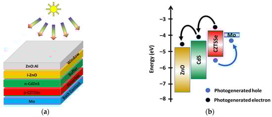
Figure 1.
(a) Main CZTSSe-based device structure, (b) energy band profile before contact of the layers displaying the main carrier flow processes.

Table 1.
Material parameters used in SCAPS-1D [29].
Table 2.
Defect parameters used in SCAPS-1D [29].
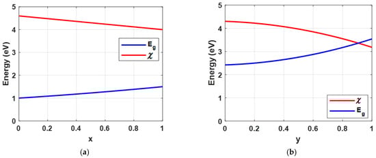
Figure 2.
Variation of Eg and χ vs. compositions for (a) absorber layer, Cu2ZnSn(SxSe1-x)4, and (b) ETL, CdyZn1-yS.
2.2. Numerical Simulation Methodology and MODELS
SCAPS-1D is a windows-based, one-dimensional solar cell modeling program. It outperforms other solar device simulator programs, and its simulation findings are promising. Herein, SCAPS-1D was used to numerically simulate device J-V characteristics to assess the proposed cell design. The structured solar cell is subjected to DC and AC analysis. Poisson’s equation, holes’ and electrons’ continuity equations, and the carrier transport equations serve as the foundation of SCAPS-1D. The involved semiconductor equations are formulated as follows:
The equations contain several variables and parameters, including Jn and Jp which represent the electron and hole current densities, R and G which denote the recombination and generation rates, n and p which indicate the carrier concentrations, which represent the charge density, and and which represent the densities of the acceptors and donors. Finally, EFn and EFp are the quasi-Fermi levels for electrons and holes.
To investigate and evaluate the performance of a solar cell in the SCAPS-1D software, the following processes were used. First, a validation step of simulated results is performed by calibrating the experimental cell against simulation results. For the given solar cell, the software is executed to find the JV characteristics whether under illumination or dark conditions. Based on the output illuminated current density, the extraction of many metrics can be conducted. These include VOC, short circuit current density (JSC), fill factor (FF), external quantum efficiency (EQE), generation and recombination rates, energy band diagrams, etc. These are some examples of the electrical measurements for AC and DC that can be simulated on SCAPS. All of these metrics are calculable and attainable under both dark and light circumstances, with various temperatures and illumination levels [30]. Additionally, SCAPS-1D offers benefits such as intuitive control, the capacity to model up to seven separate films with non-routine measurements (C-V, C-f), and tandems [31].
3. Results and Discussion
In this section, we present all obtained simulation results and a discussion of each finding. Numerical simulation allows several studies to receive an optimized structure of the solar cell. The section is divided into different subsections. Firstly, there are the calibration of this simulation work and the published experimental work to make sure the simulation results meet the practical applications. The obtained current density, voltage curve and main performance parameters, short circuit current density, open circuit voltage, fill factor, and power conversion efficiency, are compared with the published experimental work. Secondly, the codesign concept is applied to the calibrated cell to enhance its output performance parameters. Moreover, the optimization of the basic parameters of the calibrated cell to enhance its performance is introduced. The optimization starts with optimizing the thickness and doping of the electron transport layer. After that, the thickness, the doping, and the bulk defect density of the absorber layer are optimized to enhance the output performance parameters.
3.1. Calibration versus Experimental Work
Measuring calibrating simulation results against experimental data is an essential step in ensuring the accuracy and reliability of computer models. This process involves adjusting the parameters of the simulation model to match the results of real-world experiments, with the aim of minimizing the discrepancy between the two. Notably, experimental data provide a benchmark against which the accuracy of simulation models can be assessed. By comparing the results of the simulation model with experimental data, researchers can identify discrepancies and refine the model to improve its accuracy. In addition, calibration helps to ensure that simulation models are not based on incorrect assumptions or oversimplifications. Thus, this work started by calibrating the simulated solar cell with a published experimental work [29]. As mentioned before, SCAPS is used to analyze the performance metrics: VOC, JSC, FF, and PCE. The JV curve is the most significant output metric to measure solar cell performance. As a sequence, the JV curves of the simulated cell and the reported experimental work [29] are illustrated in Figure 3. It can be deduced from Figure 3 that the simulated device using SCAPS-1D agrees with the experiment [29]. By neglecting the series and shunt resistances of the cell in the simulation, the performance metrics of the two cells are given in Table 3 for the purpose of comparison with the same thickness and doping as in the experimental [29].
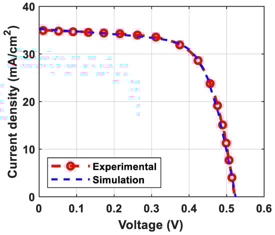
Figure 3.
JV curves of the experimental work vs. the calibrated simulation [29].
Table 3.
The output performance factors of the simulation vs. the experimental results [29].
The performance factors obtained from the experiment and simulation results in Table 3 show a slightly higher JSC than the experimental results, which is most probably due to a better photo-absorption in the absorber layer. It is worth mentioning that the shading loss in the front metal contact on the top is ignored due to the one-dimensional geometry considered, which will influence it by reducing JSC [32]. A very small difference between VOC measures can be noticed, which might result from the multiple reflections from the interfaces, mechanisms which are not included in SCAPS [33]. The fill factor and the power conversion efficiency have a subtle difference of less than 0.1%. The output performance parameters, VOC, JSC, FF, and PCE, besides the JV curves of the experimental work [29], and the simulated solar cell show the validity of the used materials parameters and design.
3.2. Codesign and Optimization
Theoretical studies give physical insight with a thorough physical explanation of the output performance. The codesign problem could be solved utilizing practical combinatorial methods, such as with an orthogonal composition gradient in the utilized layers [34]. CuSbCh2 [35], Cu2ZnSnCh4 [36], CIGS [37], and CdTe [38] absorbers or CdS [39], CuxZn1-xS [40], Zn–Ni–Co–O [41], and MgxZn1-xO transport layers are being compositionally graded and investigated using combinatorial methods [42].
In this part of the design, the composition x of the Cu2ZnSn(SxSe1-x)4 absorber is tuned to adjust the electron affinity and the energy bandgap, and composition y of the CdyZn1-yS ETL is concurrently adjusted to achieve the optimum efficiency. Figure 4a illustrates the PCE variation with the composition x (of the absorber) and composition y (of the ETL). As illustrated in the figure, the optimum PCEs are achieved in two points: point 1 (x = 0.8, y = 0.52) and point 2 (x = 0.7, y = 0.14), with a PCE exceeding 14%. The illuminated JV characteristics of the initial design and the two optimum case cells are illustrated in Figure 4b. The simulation results reveal a boost in the VOC of the codesign compared to the initial cell. This necessitates the usefulness of the codesign technique in alleviating the VOC deficit encountered in this type of thin-film solar cell. The performance metrics (VOC, JSC, FF, and PCE) of the initial design and the two optimum cases are listed in Table 4 for comparison.
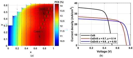
Figure 4.
(a) The PCE variation with x of Cu2ZnSn(SxSe1-x)4 absorber and y of CdyZn1-yS and (b) JV characteristics of the initial design and the two optimum cases cells.
Table 4.
The output performance parameters of the initial design, and the two optimum cases.
To give a physical insight into the previous results, the issue of band alignment, which is responsible for such results, is highlighted. Notably, reducing the charge recombination at the interface between ETL and the absorber is very important to enhance carrier extraction. To accomplish this, the CBO at the ETL/absorber interface should be 0–0.3 eV [43], where the CBO is given with Equation (6),
where and are the affinities of the photoactive layer and ETL, respectively. Figure 5 illustrates the CBO dependence on different x and y values. The affinities of the ETL and the absorber with their corresponding energy gaps are listed in Table 5 for the three scenarios.
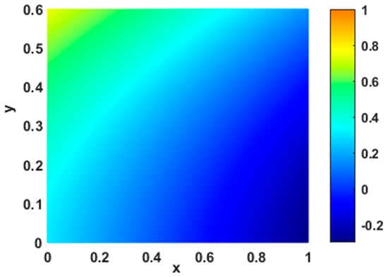
Figure 5.
CBO dependence on x and y.
Table 5.
Main band parameters of the initial design and the two optimum cases.
Based on the theoretical calculations of Shockley and Queisser who reported that the maximum PCE can be achieved for an energy gap of 1.34 eV [44], it is expected that a higher PCE is achieved (with respect to the calibrated cell) when the energy gap ≅ 1.33 eV (which corresponds to x = 0.7). However, the highest PCE is obtained for a slightly higher bandgap of about 1.38 eV (which corresponds to x = 0.8), as indicated in Table 4. This can be attributed to the crucial role of the CBO as illustrated in Figure 6, which shows the energy band diagrams of these two cases compared to the initial structure. Although the initial design reveals a favorable spike-like band offset as Figure 6a signifies, the low bandgap results in a lower PCE. For the case of Eg = 1.33, a CBO of −0.073 eV is obtained (Figure 6b and Table 5), which corresponds to an unfavorable cliff-like band. Conversely, a CBO of 0.175 eV is observed for Eg = 1.38 eV (see Figure 6c and Table 5), signifying a favorable low spike-like band offset. These interesting results show the importance of the alloy codesign as the sole design of the absorber parameters may not be sufficient to optimize the cell performance. Instead, the ETL should be simultaneously designed with the absorber to meet both superior absorption and band alignment at the same time.
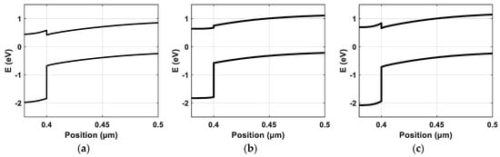
Figure 6.
The energy band diagram of (a) the initial calibrated cell, (b) optimized case 1, and (c) optimized case 2.
Furthermore, the optimization after the alloy composition codesign of the ETL and absorber compositions started with optimizing the thickness and doping of the ETL of the two optimum cases as illustrated in Figure 7. Figure 7a demonstrates that the performance improves at a certain thickness for both cases of composition. Since most of the photons with short wavelength are absorbed near the surface, it is desirable to have a thinner ETL. As can be deduced from Figure 7a, the optimum thickness is around 0.02 µm with PCEs of ≅14.13%, and 14.3% for cases 1 and 2, respectively. Additionally, one can observe in Figure 7b that varying the doping concentration from 1018 cm−3 to 1020 cm−3 results in an increase in the PCE. The highest efficiency is achieved approximately in the range 5 × 1019 cm−3 to 1020 cm−3 due to an increase in conductivity. The PCE increases to about 14.3% for the two cases, as shown with a slightly higher PCE for x = 0.7.
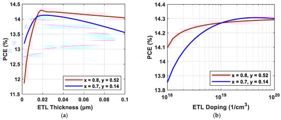
Figure 7.
Optimization of ETL parameters: (a) the thickness and (b) the doping.
The influence of the thickness, the doping concentration, and the defect density of the absorber material on the PCE has been investigated as illustrated in Figure 8. The thickness of the photoactive layer is a critical factor since it is responsible for absorbing the incident photons. However, it should not be excessively thick to allow for an effective collection of the photogenerated carriers before recombination. In the simulation, the thickness of the absorber layer varied from 0.3 μm to 2 μm, as depicted in Figure 8a. As can be inferred from the figure, the PCE does not show a significant effect from increasing absorber thickness beyond 1 µm. Further, decreasing the doping of the absorber material makes a gradient doping at the interface between the absorber and the ETL, which raises the diffusion current and enhances the PCE, as can be inferred from Figure 8b. Additionally, the higher doping concentration leads to an improved built-in electric field, facilitating better charge-carrier separation and ultimately enhancing the overall performance of the cell. However, it is important to note that further increasing the doping concentration can result in a higher recombination rate. This phenomenon is not conducive to an increase in the open-circuit voltage and, consequently, the PCE. Therefore, there is a delicate balance to be maintained, ensuring optimal doping concentrations for achieving the desired cell performance. As can be deduced from Figure 8b, the optimum doping level for the absorber layer in both scenarios is cm−3.
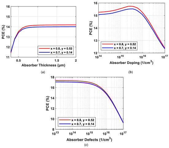
Figure 8.
Optimization of the absorber parameters: (a) the thickness, (b) the doping, and (c) the bulk defects.
Moreover, the bulk defects of the absorber material have a great influence on the PCE. As can be inferred from Figure 8c, there is no significant improvement in the PCE below the defect density of 1014 cm−3. The optimum factors of the previous optimization are listed in Table 6. Combining these optimization steps yields a high VOC of 0.8 V, a JSC of 28.97 mA/cm2, a FF of 73.72%, and a PCE of 17.16%. The JV and EQE curves of the initial and optimum cells are illustrated in Figure 9 for comparison.
Table 6.
The optimum technological factors of the ETL and the absorber layer.
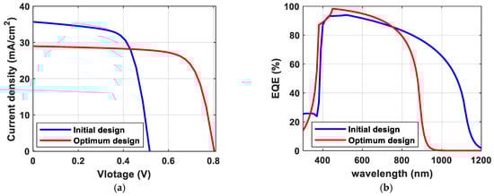
Figure 9.
(a) The JV characteristics of the initial design, and the optimized one, and (b) the EQE spectra.
To compare this work with some recent publications in the literature, a group of similar structures has been collected and illustrated in Table 7. In [45], the PCE of the CZTSSe solar cell device has been notably increased from 7.4% to 8.5% by adding Zn to the CdS buffer layer. In [46], a study aimed to investigate the effect of three different buffer layers, namely CdS, ZnS, and CdZnS, on the performance parameters of CZTS solar cells through numerical simulations. The simulation results showed that a CdZnS buffer layer achieves high efficiency CZTS solar cells. PCEs utilizing these buffer layers were around 11.20%. In [47], the utilization of a CdZnS buffer layer has resulted in a 13.23% conversion efficiency in CZTS solar cells, which is an improvement over the conventional buffer layer, CdS, that only yielded 12.61%. In [48], compared to the CZTS/CdS device, the CZTS/CdZnS device exhibited an increase in both the conversion efficiency and fill factor. Specifically, the PCE increased from 2.31% to 4.88%.
Table 7.
Comparison of different structures based on CZTSSe photovoltaic devices utilizing CdZnS as buffer layers.
Finally, the co-design of the elemental compositions of the electron transport layer (ETL) and the absorber represents a new field, and its widespread application across various materials has not been widely explored. One of these few efforts was devoted to the codesign of alloy compositions of CdSexTe1_x (as an absorber material) and MgyZn1-yO (as an ETL) [49]. In their experimental study, the authors revealed that the solar cell performance is a strongly coupled function of both x and y compositions. They achieved a PCE of up to 17.7% at specific atomic compositions (x = 0.04 and y = 0.18) [49]. As this field of research is advancing, a need for simulation studies is mandatory to investigate and evaluate new material systems and to provide design guidelines for the corresponding solar cells. This study serves as a significant contribution by shedding light on this emerging field, paving the way for further advancements.
4. Conclusions
Photovoltaics are the most effective solution to the energy demand issue. Utilizing new materials and designs are required to meet the solution to this issue. CZTSSe-based solar cells have a promising future according to their unique set of optical and electrical parameters, in addition to their abundance. CdZnS is a good candidate for traditional ETMs. Using the alloy composition codesign concept improves solar cell performance. In this context, a Cd0.48Zn0.52S with an absorber composition of x = 0.8 is found to be the optimum criterion in the proposed cell with a PCE of 14.21%. This choice integrates both a suitable bandgap of 1.38 eV with a favorable low spike band offset. Further, optimizing the ETL thickness and doping yields a PCE exceeding 14.3%. After optimizing the thickness and concentration of the absorber film, a PCE of 15.65% was achieved. The bulk defects in the absorber layer have a substantial influence on the PCE. Decreasing the defect density resulted in increasing the PCE. In the investigated cell, no significant PCE improvement below Nt of 1014 cm−3 has been attained, and a PCE of 17.16% was achieved at this value. This simulation-based study offered the advantage of gaining insight into the optimization of the cell performance of CZTSSe-based devices by enabling a comprehensive exploration of the alloy composition codesign of both the absorber and the ETL to surmount the VOC deficit of this kind of solar cell which is considered the main issue in developing CZTSSe-based solar cells.
Author Contributions
Conceptualization, A.S., M.M.S. and W.Z.; methodology, A.S., M.M.S. and W.Z.; validation and formal analysis, T.I.A., M.M.S. and W.Z.; visualization, T.I.A. and W.Z.; investigation, all authors; writing—original draft preparation, all authors; writing—review and editing, A.S. and M.M.S. All authors have read and agreed to the published version of the manuscript.
Funding
This research received no external funding.
Data Availability Statement
No new data were created or analyzed in this study. Data sharing does not apply to this article.
Conflicts of Interest
The authors declare no conflict of interest.
References
- Renewables 2019—Analysis—IEA. Available online: https://www.iea.org/reports/renewables-2019 (accessed on 1 March 2023).
- Okil, M.; Salem, M.S.; Abdolkader, T.M.; Shaker, A. From Crystalline to Low-cost Silicon-based Solar Cells: A Review. Silicon 2021, 14, 1895–1911. [Google Scholar] [CrossRef]
- Salem, M.S.; Zekry, A.; Shaker, A.; Abouelatta, M. Design and simulation of proposed low cost solar cell structures based on heavily doped silicon wafers. In Proceedings of the 2016 IEEE 43rd Photovoltaic Specialists Conference (PVSC), Portland, OR, USA, 5–10 June 2016; pp. 2393–2397. [Google Scholar] [CrossRef]
- Zhang, Y.; Liu, H. Nanowires for High-Efficiency, Low-Cost Solar Photovoltaics. Crystals 2019, 9, 87. [Google Scholar] [CrossRef]
- Salem, M.S.; Alzahrani, A.J.; Ramadan, R.A.; Alanazi, A.; Shaker, A.; Abouelatta, M.; Gontrand, C.; Elbanna, M.; Zekry, A. Physically Based Analytical Model of Heavily Doped Silicon Wafers Based Proposed Solar Cell Microstructure. IEEE Access 2020, 8, 138898–138906. [Google Scholar] [CrossRef]
- Salhi, B. The Photovoltaic Cell Based on CIGS: Principles and Technologies. Materials 2022, 15, 1908. [Google Scholar] [CrossRef] [PubMed]
- Mabvuer, F.T.; Nya, F.T.; Kenfack, G.M.D.; Laref, A. Lowering Cost Approach for CIGS-Based Solar Cell Through Optimizing Band Gap Profile and Doping of Stacked Active Layers—SCAPS Modeling. ACS Omega 2023, 8, 3917–3928. [Google Scholar] [CrossRef] [PubMed]
- Alanazi, T.I. Current spray-coating approaches to manufacture perovskite solar cells. Results Phys. 2023, 44, 106144. [Google Scholar] [CrossRef]
- Khattak, Y.H.; Baig, F.; Toura, H.; Ullah, S.; Marí, B.; Beg, S.; Ullah, H. Effect of CZTSe BSF and minority carrier life time on the efficiency enhancement of CZTS kesterite solar cell. Curr. Appl. Phys. 2018, 18, 633–641. [Google Scholar] [CrossRef]
- Mohammadnejad, S.; Parashkouh, A.B. CZTSSe solar cell efficiency improvement using a new band-gap grading model in absorber layer. Appl. Phys. A 2017, 123, 758. [Google Scholar] [CrossRef]
- Et-Taya, L.; Ouslimane, T.; Benami, A. Numerical analysis of earth-abundant Cu2ZnSn(SxSe1-x)4 solar cells based on Spectroscopic Ellipsometry results by using SCAPS-1D. Sol. Energy 2020, 201, 827–835. [Google Scholar] [CrossRef]
- Kim, J.; Hiroi, H.; Todorov, T.K.; Gunawan, O.; Kuwahara, M.; Gokmen, T.; Nair, D.; Hopstaken, M.; Shin, B.; Lee, Y.S.; et al. High Efficiency Cu2ZnSn(S,Se)4Solar Cells by Applying a Double In2S3/CdS Emitter. Adv. Mater. 2014, 26, 7427–7431. [Google Scholar] [CrossRef]
- Yang, K.-J.; Son, D.-H.; Sung, S.-J.; Sim, J.-H.; Kim, Y.-I.; Park, S.-N.; Jeon, D.-H.; Kim, J.; Hwang, D.-K.; Jeon, C.-W.; et al. A band-gap-graded CZTSSe solar cell with 12.3% efficiency. J. Mater. Chem. A 2016, 4, 10151–10158. [Google Scholar] [CrossRef]
- Rühle, S. Tabulated values of the Shockley–Queisser limit for single junction solar cells. Sol. Energy 2016, 130, 139–147. [Google Scholar] [CrossRef]
- Dermenji, L.; Guc, M.; Gurieva, G.; Dittrich, T.; Rappich, J.; Curmei, N.; Bruc, L.; Sherban, D.; Simashkevich, A.; Schorr, S.; et al. Thin films of (AgxCu1−x)2ZnSn(S,Se)4 (x = 0.05–0.20) prepared by spray pyrolysis. Thin Solid Films 2019, 690, 137532. [Google Scholar] [CrossRef]
- Li, S.; Lloyd, M.A.; McCandless, B.E.; Baxter, J.B. Effects of cation composition on carrier dynamics and photovoltaic performance in Cu2ZnSnSe4 monocrystal solar cells. Sol. Energy Mater. Sol. Cells 2020, 205, 110255. [Google Scholar] [CrossRef]
- Gao, S.; Jiang, Z.; Wu, L.; Ao, J.; Zeng, Y.; Sun, Y.; Zhang, Y. Interfaces of high-efficiency kesterite Cu2ZnSnS(e)4thin film solar cells. Chin. Phys. B 2018, 27, 018803. [Google Scholar] [CrossRef]
- Basyoni, M.S.S.; Salah, M.M.; Mousa, M.; Shaker, A.; Zekry, A.; Abouelatta, M.; Alshammari, M.T.; Al-Dhlan, K.A.; Gontrand, C. On the Investigation of Interface Defects of Solar Cells: Lead-Based vs Lead-Free Perovskite. IEEE Access 2021, 9, 130221–130232. [Google Scholar] [CrossRef]
- Yan, C.; Sun, K.; Liu, F.; Huang, J.; Zhou, F.; Hao, X. Boost Voc of pure sulfide kesterite solar cell via a double CZTS layer stacks. Sol. Energy Mater. Sol. Cells 2017, 160, 7–11. [Google Scholar] [CrossRef]
- Kim, J.; Park, S.; Ryu, S.; Oh, J.; Shin, B. Improving the open-circuit voltage of Cu2ZnSnSe4 thin film solar cells via interface passivation. Prog. Photovolt. Res. Appl. 2017, 25, 308–317. [Google Scholar] [CrossRef]
- Enkhbat, T.; Enkhbayar, E.; Sharif, H.; Mina, S.; Song, S.; Kim, J. Insights into High-Efficiency Ag-Alloyed CZTSSe Solar Cells Fabricated through Aqueous Spray Deposition. ACS Appl. Mater. Interfaces 2021, 13, 45426–45434. [Google Scholar] [CrossRef]
- O’Neill, A.; Jo, E.; Choi, E.; Park, J.; Kim, J.H.; Yun, J.S.; Seidel, J. Enhancing CZTSSe solar cells through electric field induced ion migration. J. Mater. Chem. A 2022, 10, 5642–5649. [Google Scholar] [CrossRef]
- Pakštas, V.; Grincienė, G.; Selskis, A.; Balakauskas, S.; Talaikis, M.; Bruc, L.; Curmei, N.; Niaura, G.; Franckevičius, M. Improvement of CZTSSe film quality and superstrate solar cell performance through optimized post-deposition annealing. Sci. Rep. 2022, 12, 1–9. [Google Scholar] [CrossRef]
- Shaker, A.; Salem, M.S.; Jayan, K.D. Analysis and design of p-n homojunction Sb2Se3 solar cells by numerical simulation. Sol. Energy 2022, 242, 276–286. [Google Scholar] [CrossRef]
- Salem, M.S.; Shaker, A.; Almurayziq, T.S.; Alshammari, M.T. Prospective efficiency boosting of full-inorganic single-junction Sb2(S, Se)3 solar cell. Sol. Energy Mater. Sol. Cells 2022, 248, 112001. [Google Scholar] [CrossRef]
- Minbashi, M.; Ghobadi, A.; Yazdani, E.; Kordbacheh, A.A.; Hajjiah, A. Efficiency enhancement of CZTSSe solar cells via screening the absorber layer by examining of different possible defects. Sci. Rep. 2020, 10, 21813. [Google Scholar] [CrossRef] [PubMed]
- Et-Taya, L.; Benami, A.; Ouslimane, T. Study of CZTSSe-Based Solar Cells with Different ETMs by SCAPS. Sustainability 2022, 14, 1916. [Google Scholar] [CrossRef]
- Pandey, K.; Patel, A.K.; Mishra, R. Numerical study on performance enhancement of CZTSSe solar cells with Cu2O and MoTe2 as hole transport layer. J. Comput. Electron. 2022, 21, 895–904. [Google Scholar] [CrossRef]
- Yousefi, M.; Minbashi, M.; Monfared, Z.; Memarian, N.; Hajjiah, A. Improving the efficiency of CZTSSe solar cells by engineering the lattice defects in the absorber layer. Sol. Energy 2020, 208, 884–893. [Google Scholar] [CrossRef]
- Burgelman, M.; Decock, K.; Niemegeers, A.; Verschraegen, J.; Degrave, S. SCAPS Manual; University of Gent: Ghent, Belgium, 2014. [Google Scholar]
- Burgelman, M.; Verschraegen, J.; Degrave, S.; Nollet, P. Modeling thin-film PV devices. Prog. Photovolt. Res. Appl. 2004, 12, 143–153. [Google Scholar] [CrossRef]
- Meher, S.; Balakrishnan, L.; Alex, Z. Analysis of Cu2ZnSnS4/CdS based photovoltaic cell: A numerical simulation approach. Superlattices Microstruct. 2016, 100, 703–722. [Google Scholar] [CrossRef]
- Smets, A.H.M.; Jäger, K.; Isabella, O.; van Swaaij, R.A.; Zeman, M. Solar Energy: The Physics and Engineering of Photovoltaic Conversion, Technologies and Systems; UIT Cambridge: Cambridge, UK, 2016; p. 462. [Google Scholar]
- Green, M.L.; Choi, C.L.; Hattrick-Simpers, J.R.; Joshi, A.M.; Takeuchi, I.; Barron, S.C.; Campo, E.; Chiang, T.; Empedocles, S.; Gregoire, J.M.; et al. Fulfilling the promise of the materials genome initiative with high-throughput experimental methodologies. Appl. Phys. Rev. 2017, 4, 011105. [Google Scholar] [CrossRef]
- Welch, A.W.; Baranowski, L.L.; Peng, H.; Hempel, H.; Eichberger, R.; Unold, T.; Lany, S.; Wolden, C.; Zakutayev, A. Trade-Offs in Thin Film Solar Cells with Layered Chalcostibite Photovoltaic Absorbers. Adv. Energy Mater. 2017, 7, 1601935. [Google Scholar] [CrossRef]
- Collord, A.D.; Xin, H.; Hillhouse, H.W. Combinatorial Exploration of the Effects of Intrinsic and Extrinsic Defects in Cu2ZnSn(S,Se)4. IEEE J. Photovolt. 2015, 5, 288–298. [Google Scholar] [CrossRef]
- Yordanov, G.H.; Midtgard, O.-M.; Saetre, T.O. Equivalent cell temperature calculation for PV modules with variable ideality factors. In Proceedings of the 2012 38th IEEE Photovoltaic Specialists Conference, Austin, TX, USA, 3–8 June 2012; Volume 2012, pp. 505–508. [Google Scholar] [CrossRef]
- Hanak, J.; Bykov, E.; Elgamel, H.; Grecu, D.; Putt, J.; Reiter, N.; Shvydka, D.; Powell, R. Rapid optimization of CdTe(1-x)Sx absorber films and PV devices by means of the combinatorial method. In Proceedings of the Conference Record of the Twenty-Eighth IEEE Photovoltaic Specialists Conference—2000 (Cat. No.00CH37036), Anchorage, AK, USA, 15–22 September 2000; pp. 495–498. [Google Scholar] [CrossRef]
- Mokurala, K.; Baranowski, L.L.; Lucas, F.W.D.S.; Siol, S.; van Hest, M.F.A.M.; Mallick, S.; Bhargava, P.; Zakutayev, A. Combinatorial Chemical Bath Deposition of CdS Contacts for Chalcogenide Photovoltaics. ACS Comb. Sci. 2016, 18, 583–589. [Google Scholar] [CrossRef]
- Woods-Robinson, R.; Han, Y.; Mangum, J.S.; Melamed, C.L.; Gorman, B.P.; Mehta, A.; Persson, K.A.; Zakutayev, A. Combinatorial Tuning of Structural and Optoelectronic Properties in CuxZn1−xS. Matter 2019, 1, 862–880. [Google Scholar] [CrossRef]
- Zakutayev, A.; Perkins, J.D.; Parilla, P.A.; Widjonarko, N.E.; Sigdel, A.K.; Berry, J.J.; Ginley, D.S. Zn-Ni-Co-O wide-band-gap p-type conductive oxides with high work functions. MRS Commun. 2011, 1, 23–26. [Google Scholar] [CrossRef]
- Rodríguez Martínez, X. Development of Organic Solar Cells by Combinatorial Methods. 2020. Available online: https://ddd.uab.cat/record/240960 (accessed on 22 March 2023).
- Minemoto, T.; Murata, M. Theoretical Analysis on Effect of Band Offsets in Perovskite Solar Cells. In Solar Energy Materials and Solar Cells; Elsevier: Amsterdam, The Netherlands, 2015; Available online: https://www.sciencedirect.com/science/article/pii/S0927024814005674 (accessed on 1 January 2023).
- Shockley, W.; Queisser, H.J. Detailed Balance Limit of Efficiency of p-n Junction Solar Cells. J. Appl. Phys. 1961, 32, 510–519. [Google Scholar] [CrossRef]
- Zhang, X.; Chen, J.; Chen, J.; Ge, L.; Li, Y.; Zhao, Y.; Wang, C. Synthesis of CdZnS buffer layer and its impact on Cu2ZnSn(S, Se)4 thin film solar cells. J. Mater. Sci. Mater. Electron. 2022, 33, 2399–2405. [Google Scholar] [CrossRef]
- Jhuma, F.A.; Shaily, M.Z.; Rashid, M.J. Towards high-efficiency CZTS solar cell through buffer layer optimization. Mater. Renew. Sustain. Energy 2019, 8, 3. [Google Scholar] [CrossRef]
- Benabbas, S.; Er, Z.; Bouchama, I.; Rouabah, Z.; Bouarissa, N.; Boudour, S.; Saeed, M.A. Optimization of Chalcogenide CdTe, CZTS and CZTSe Solar Cells PerformancesUsing Cd1-xZnxS Buffer Layer Dilute magnetic semiconductors View project Defect Analysis & computational physics View project Zahir Rouabah. Iran. J. Chem. Chem. Eng. Int. 2022, 41, 1360–1369. [Google Scholar] [CrossRef]
- Sun, S.; Guo, J.; Hao, R.; Aierken, A.; Liu, B.; Gu, K.; Wang, L.; Ma, X.; Wei, G.; Cai, J.; et al. Influence of Cd0.6Zn0.4S buffer layer on the band alignment and the performance of CZTS thin film solar cells. Opt. Mater. 2020, 112, 110666. [Google Scholar] [CrossRef]
- Khan, I.S.; Ablekim, T.; McGott, D.L.; Good, B.; Perkins, C.L.; Metzger, W.K.; Zakutayev, A. Codesigning Alloy Compositions of CdSeyTe1−y Absorbers and MgxZn1−xO Contacts to Increase Solar Cell Efficiency. Sol. RRL 2022, 6, 2200394. [Google Scholar] [CrossRef]


Disclaimer/Publisher’s Note: The statements, opinions and data contained in all publications are solely those of the individual author(s) and contributor(s) and not of MDPI and/or the editor(s). MDPI and/or the editor(s) disclaim responsibility for any injury to people or property resulting from any ideas, methods, instructions or products referred to in the content. |
© 2023 by the authors. Licensee MDPI, Basel, Switzerland. This article is an open access article distributed under the terms and conditions of the Creative Commons Attribution (CC BY) license (https://creativecommons.org/licenses/by/4.0/).