Abstract
The conventional resonant inductor–inductor–capacitor (L2C) DC–DC converters have the major drawbacks of poor regulation, improper current sharing, load current ripples, conduction losses, and limiting the power levels to operate at higher loads for electric vehicle (EV) charging systems. To address the issues of the L2C converter, this paper proposes an interleaved inductor–inductor–capacitor (iL2C) full-bridge (FB) DC–DC converter as an EV charger with wide input voltage conditions. It comprises two L2C converters operating in parallel on the primary side with 8-GaN switches and maintains the single rectifier circuit on the secondary side as common. Further, it introduces the hybrid control strategy called variable frequency + phase shift modulation (VFPSM) technique for iL2C with a constant voltage charging mode operation. The design requirements, modeling, dynamic responses, and operation of an iL2C converter with a controller are discussed. The analysis of the proposed concept designed and simulated with an input voltage of 400 Vin at a load voltage of 48 V0 presented at different load conditions, i.e., full load (3.3 kW), half load (1.65 kW), and light load (330 W). The dynamic performances of the converter during line and load regulations are presented at assorted input voltages. In addition, to analyze the controller and converter performance, the concept was validated experimentally for wide input voltage applications of 300–500 Vin with a desired output of 48 V0 at full load condition, i.e., 3.3 kW and the practical efficiency of the iL2C converter was 98.2% at full load.
1. Introduction
These days, conventional internal combustion engines (ICEs) are becoming saturated due to a deficiency of fossil resources, and the environment is polluted with toxic gases, carbon emissions, and drastic climate changes. Considering this, there is a global call for implementing clean energy transportation to safeguard against climatic changes. Recently, EVs as an eco-friendly power source have gained significant popularity, with the promising objective of replacing ICEs and reducing CO2 emissions [1]. Electrifying the transportation sector with battery electric vehicles (BEVs), fuel-cell electric vehicles (FCEVs), hybrid electric vehicles (HEVs), ultra-capacitor electric vehicles (UCEVs), supercapacitor electric vehicles (SCEVs), and plugin hybrid electric vehicles (PHEVs) can significantly reduce emission rates. The industry is advancing toward the adoption of electric vehicles achieve net-zero emissions by 2030 in Europe and 2050 in India. Due to the increasing demand for EVs, the development of charging topologies that are more reliable and efficient is essential. There are several charging topologies in terms of power electronics architectures for applications such as solar, EV, etc., with optimizing methods discussed in [2,3,4]. The typical block diagram of a charging architecture is shown in Figure 1.
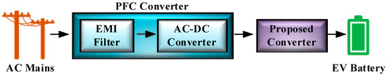
Figure 1.
Typical block diagram of an EV charging power conversion system.
During the past decade, much research has been conducted on a wide variety of DC–DC converters for various applications such as electric vehicles, photovoltaics, and fuel cell applications [5,6]. Many L2C resonant converters are gaining popularity due to their merits of zero voltage switching (ZVS) operation on the primary side at all load conditions and zero current switching (ZCS) operation on the secondary side with synchronous rectification, wide voltage gain, the ability to provide soft switching characteristics, and high power density with high switching frequency capability [7,8]. Additionally, the dv/dt at the primary side of the circuit is smaller due to the L2C converter’s lower turn-off current, resulting in lower electromagnetic interference (EMI) [9,10].
A typical L2C Resonant FB DC–DC converter is shown in Figure 2. It consists of a series resonant tank, which includes an inductor Lr and capacitor Cr in series with a high-frequency transformer to provide sufficient galvanic isolation, and a parallel inductance also available in the resonant tank, which is called magnetizing inductance Lm to form the resonant network [11]. For wide voltage gain applications, the switching frequency fs must vary in a wide range, and the designer needs to take care of the ZVS function because it may be lost if the switching frequency is too low. The effect of the junction capacitance Cj, as discussed in [12], of secondary side rectifying diodes causes poor voltage control when fs exceeds the resonant frequency fr. The magnetic component size is constrained by the low switching frequency fs. As a result, designing an L2C converter with a broad output voltage range poses considerable challenges, and performance degrades rapidly as fs deviates from fr [13,14]. In general, there are three different modes of operation in a L2C converter, including above resonance, below resonance, and at resonance. During all these modes of operation, the regulation control on the ZCS region is fully achieved, but in the case of the ZVS region, there is poor performance in regulation at different load conditions with variable input voltages. Additionally, to utilize the L2C converter as an EV charger, there are certain limitations such as increasing the load capacity to operate at higher power levels, current and voltage ripples at the output side causing damage to the product, and the efficiency at high power levels being low [15].
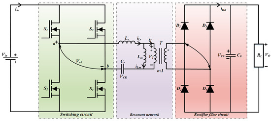
Figure 2.
L2C resonant FB DC–DC power converter.
To overcome the drawbacks of the L2C converter, this paper considered a two-stage interleaved L2C (iL2C) converter. Due to the resonant tank design of L2C, the load capacity is limited, which results in an increased circulating current and thereby lower efficiency. Using iL2C this problem can be solved by adding the L2C in parallel to double the load capacity [16]. Additionally, at high current applications, the major power loss component is the transformer, which has eddy current loss (AC loss) and winding losses of copper resistance (DC loss), and splitting the circuit transformer current reduces the losses of AC and DC. Using the interleaving technique reduces the current ripples [17].
To date, numerous control strategies have been defined to provide soft switching, tight regulation, and reduce the circulating current [18,19]. These methods are operated by adding the transformer current via injecting zero-voltage on the primary or secondary side, and this can also be obtained by changing the phase shifting method. Some papers suggested [18,19] that different control strategies can be used at different regions such as fs < fr, fs = fr and fs > fr but this affects the regulation. Rather than using the zero-voltage sequence method and other techniques mentioned to extend the soft switching region [20], this paper proposes a hybrid control strategy called the VFPSM technique for iL2C FB converter. It is based on switching at a predefined current value. The proposed scheme allows either a ZCS or ZVS depending on how the designer chooses the switching current level. In addition, it also minimizes the root mean square (RMS) current in the transformer by fixing the predefined value of reactive current [21,22]. Hence, it provides an additional advantage to the controller concerning conventional phase shift modulation between the primary and secondary of transformer [23,24]. Additionally, with this method, soft switching can be achieved with low conduction losses, and proper load and line regulations are conducted and increase the system’s efficiency. Meanwhile, there are certain limitations, such as its complicated design, which require proper tuning of control parameters [25,26].
Furthermore, this paper also sheds light on the GaN-HEMT-based technology’s implementation on the proposed system [27,28]. The superior characteristics of GaN technology compared to Si (silicon), such as a wideband gap, reliability, packaging, heating, efficiency, and operating at high power density with frequency, serve as major advantages of GaN technology [29]. To reduce the losses at high power operation, a lower Rdson is required to improve the efficiency of the entire system to confer more reliable operation at higher switching speeds [30].
The main research contributions of this paper are summarized below:
- Modeling of iL2C converter topology was carried out to enhance the load capacity, reduce the current ripples, and reduce the circulating current;
- A hybrid control strategy was introduced across all operating modes to improve the regulation, minimize switching losses, and enable soft switching;
- Theoretical and simulation analysis was performed for various load conditions of the converter, including full load, half load, and light load with load regulation of the voltage, and current was also described;
- To examine the controller performance, simulations were performed for variable input voltages with line regulation of load voltage, and current deviations were determined;
- An experimental prototype for a 3.3 kW electric vehicle charger was demonstrated using GaN-HEMT technology;
- Furthermore, the highlights of the entire theoretical, simulation, and experimental validations were discussed for steady-state and transient voltage and current ripples at the load side.
The organization of this paper is as follows. Section 1 presents the introduction and literature overview. Section 2 details the iL2C resonant FB converter topology with the working principle, followed by detailed analysis of the design parameters in Section 3. In Section 4, we discuss the proposed control strategy and present its detailed design. Section 5 provides the simulation results and various case studies, while experimental results and validation are detailed in Section 6. Section 7 presents the converter’s dynamic performance analysis under line and load regulations. Section 8 details the outcomes and conclusions of the proposed research work.
2. Interleaved L2C Resonant FB DC–DC Converter Topology and the Working Principle
A typical iL2C resonant FB DC–DC converter topology is shown in Figure 3 and key waveforms are presented in Figure 4. It consists of two resonant tanks, two switching circuits, and a single diode rectifier circuit [24]. The primary side employs two L2C resonant switching circuits called converter 1 and converter 2 connected in parallel, and secondary side is outfitted with two transformer secondary windings with a single rectifier network. The proposed technique provides operation in a phase shift angle of 180° of phase difference between the gate signals of converter 1 and converter 2, and the resonant frequency of he converter 1 is defined in Equation (1). Since the two converters’ operation is identical, all the equations and circuit operation are discussed for converter 1 with resonant network 1.
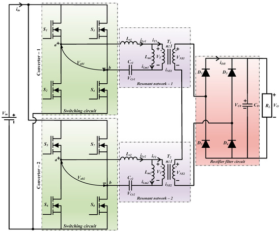
Figure 3.
Typical structure of an iL2C resonant FB DC–DC power converter topology.
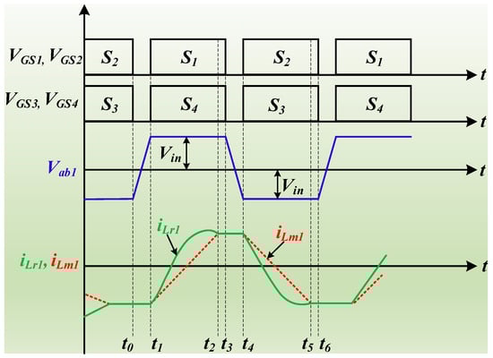
Figure 4.
Key identical waveforms of iL2C resonant FB DC–DC power converter 1.
Mode 1: Before t0, the switch S2 and S3 are turned ON with all the secondary side diodes in the OFF condition. At the point of t0–t1, the switches S2 and S3 are turned OFF, and the body diodes of S1 and S4 are ON with the negative resonant current of iLr1.
Mode 2: During t1–t2, the switch S1 and S4 are turned ON and the voltage Vab1 at transformer 1 T1 is equal to input voltage Vin. The resonant inductor Lr1 starts resonating with resonant capacitor Cr1; meanwhile, filter capacitor C0 is discharged through the secondary current of iNS1. Additionally, diodes D1 and D4 are in the ON condition with the flow of current and voltage. The voltage at magnetizing inductance Lm1 is defined in the following Equation (2) and the current across the iLm1 increases linearly. At this period, the voltage at VNS1 is equal to the output voltage, which is defined in Equation (3),
The state space equation during stage 2 is defined in Equation (4) below:
Mode 3: During the period t2–t3, the switches S1 and S4 are turned OFF; due to the positive flow of the current at iLr1, the switches S2 and S3 are turned ON with all the secondary side diodes in the OFF condition.
Mode 4: During the period t3–t4, the switches S2 and S3 are turned ON; because of negative current flow in iNS1 the secondary side diodes, D2 and D4 are ON. Therefore, the voltage at the secondary side of the transformer is defined by −VC0 with very low voltage, and hence the current iLm1 decreases linearly. The resonant inductor Lr1 starts resonating with resonant capacitor Cr1; meanwhile, filter capacitor C0 is charged through the secondary current of iNS1. At this period, the voltage VNS1 is given as follows:
The state space equation during stage 4 is defined in Equation (6) below:
Mode 5: During the period t4–t5, D2 and D3 are in the ON state with the secondary side transformer current iNS1 going to zero. The secondary side of the transformer voltage is denoted by Equation (7), and respective to that the magnetizing inductance decreases slowly. Furthermore, the resonant inductor Lr1 starts resonating with the resonant capacitor Cr1.
The state space equation during stage 5 is defined in Equation (8) below:
Mode 6: During the period t5–t6, the secondary side of the transformer current iNS1 is completely zero with all the diodes in the OFF condition. At this period, the magnetizing inductance iLm1 starts resonating with resonant capacitor Cr1 and inductor Lr1.
After evaluating all the gains at peak values, we can define the ideal curve, as shown in Figure 5; if the frequency is 1, then the converter is operating at a resonance condition where fs = fr; likewise, if the frequency is less than 1, the converter is operating at below the resonance condition where fs < fr, and similarly, if the frequency is greater than 1, then the converter is operating above the resonance condition, where fs > fr [31].
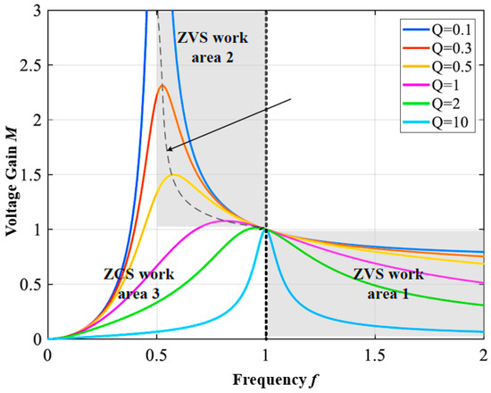
Figure 5.
Voltage gain M vs. frequency f by varying the Q-factor.
3. Parameter Design
This section deals with the step-by-step design calculations of the iL2C converter for all the components and their associated critical values [32]. Since converter 1 and converter 2 are identical in operation, the parametric design was calculated for converter 1. The main system parameters are shown in Table 1 and the AC equivalent circuit of LLC converter 1 is shown in Figure 6.

Table 1.
Main parameters of an EV charger powered by an iL2C resonant DC–DC converter.
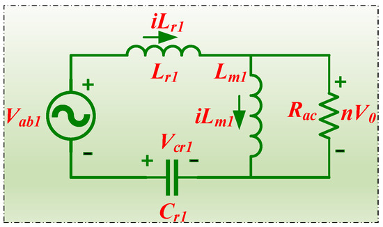
Figure 6.
Equivalent AC–circuit of LLC converter 1.
The transformer T1 turning ratio and maximum and minimum values of the voltage gain of the iL2C converter at rated operating conditions are derived in Equations (9)–(11) [33,34].
where n is transformer turning ratio, Vin_max and Vin_min are maximum and minimum input voltages, V0_max and V0_min are maximum and minimum output voltages, and Mmax and Mmin are the maximum and minimum voltage gain.
The value of the inductor ratio Lactual is determined in the following Equation (12), where fn represents the switching frequency. When the switching frequency is adjusted to the maximum value, the output from the previous step ensures that the converter enters the cut-off mode at the minimum output and maximum input [35].
At the next step, we consider the resonant tank design of resonant inductance Lr1, capacitance Cr1, impedance Z01, and magnetizing inductance Lm1 with equivalent resistance Rac1 in the following Equations (13)–(17). The resonant inductor is derived from Equation (12) and the magnetizing inductance of the converter. The equivalent resistance of the converter circuit is derived using Equation (13) followed by other critical equations.
The critical operating values of conversion gain Mcrit, maximum impedance Z0, input current Iin_crit, output voltage V0_crit, and current I0_crit are determined in Equations (18)–(22), where P0_max is the output power and η is the efficiency [36,37].
The other important parametric Equations (23)–(27) are the quality factors of minimum Qmin and maximum Qmax, and the switching frequency of fn_max and fn_min, where Rac_max and Rac_min are the equivalent resistance of the maximum and minimum values, respectively, Iin_max is the input maximum current, and fn_max and fn_min are the switching frequency of the maximum and minimum values, respectively; further, fn_max is 1.8 times the resonant frequency of fr.
4. Hybrid Control Strategy
There are many control methods available currently in research on frequency modulation and phase shifting strategies, but in practice, they have their own drawbacks, namely, the converter has wide input and output voltage operations. In general, the phase shifting strategy is easy to design but complicated at wide input voltage ranges, and frequency modulation is an effective but complicated magnetic design. This paper proposes the combination of a hybrid control strategy named as the VFPSM technique for an iL2C converter, which operates at all conditions with the same control strategy, unlike those in [25,26].
The generation of switching frequency fs was carried out based on the provided error voltage by taking the output voltage Vo and comparing it with the reference input voltage Vref. The comparison of input and output voltage references can be completed by using the Voltage Control Oscillator (VCO), which also drives the gate signals. The controller will control the output voltage Vo and vary the current, which is called the CV mode of operation, and the control circuit is shown in Figure 7. The design of the outer feedback compensator is greatly aided by the third-order transfer function mentioned in Equation (28), where the sub equations in the transfer function are discussed in Equations (29)–(33).
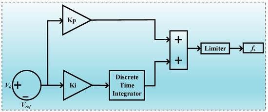
Figure 7.
Voltage control oscillator block diagram for the constant voltage mode.
Generating the switching frequency from Figure 7 provides pulse generation to the switches. The phase shift of the 180° degree method was used to regulate the high input voltage over the broad range from 300–500 Vin and the VFPSM technique provided tight regulation of the line and load voltage and current. The switching operation of converter 1 and converter 2 is based on the phase shifting methodology termed as before 180° and after 180°, and the typical switching control circuit is shown in Figure 8.
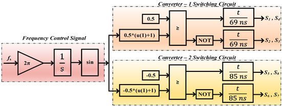
Figure 8.
VFPSM control strategy control block diagram.
5. Simulation Results and Analysis
The simulation analysis was carried out in MATLAB/Simulink to check the performance of the proposed iL2C converter with the VFPSM control technique. The actual design values of the converter were simulated and are tabulated in Table 2. The simulated analysis is presented for different case studies in the first case, and the nominal input and nominal output voltage at full load conditions were analyzed. In the next two cases, the converter was analyzed for half load and light load conditions at nominal voltage values; in addition to that, the load regulation of the voltage and current is presented. In the next step, two cases were performed to examine the hybrid controller: a variable step change in input voltages from 300–500 Vin and 500–300 Vin with a constant output voltage of 48 V0 at full load condition, which is discussed in terms of the line regulation of the load voltage and current.
Table 2.
Modeling parameters of the iL2C Converter.
5.1. Case 1: Performance Analysis of the Converter for a Nominal Input Voltage (400 Vin) with a Fixed Output Voltage (48 V0) at Full Load Condition, i.e., 3.3 kW
This section analyzes the performance of the iL2C converter at a full load condition, i.e., 3.3 kW. Figure 9 shows the nominal input voltage of 400 Vin as the constant. The converter simulated results were examined with a controlled nominal load voltage and current of 48 V0 and 68.75 A at a full load condition, i.e., 3.3 kW, which is presented in Figure 10. The ripple voltage and currents were found with a voltage deviation of +0.5 V (+1.04%) at a rated output of 48 V0 and the current deviation is around +0.65 A (+0.94%) at a full load current of 68.75 A.
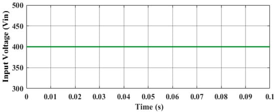
Figure 9.
Nominal input voltage waveform (Vin = 400 V).
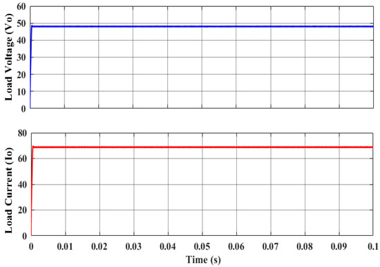
Figure 10.
Load voltage and current waveforms (V0 = 48 V, I0 = 68.75 A).
5.2. Case 2: Performance Analysis of the Converter for a Nominal Input Voltage (400 Vin) with a Fixed Output Voltage (48 V0) at a Half Load Condition, i.e., 1.65 kW
In this case, the converter operation was simulated at half of the load of the full load condition, which is at 1.65 kW. The nominal load voltage of 48 V0 and load current of 38.375 A at a half load condition are presented in Figure 11. The ripple voltage and currents were found with a voltage deviation of +0.3 V (+0.62%) at a rated output of 48 V0 and the current deviation was around +0.175 A (+0.5%) at a half load current of 38.375 A.
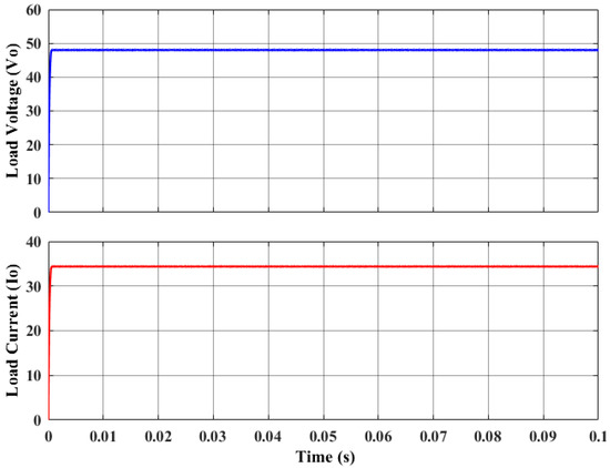
Figure 11.
Load voltage and current waveforms (V0 = 48 V, I0 = 38.375 A).
5.3. Case 3: Performance Analysis of the Converter for a Nominal Input Voltage (400 Vin) with a Fixed Output Voltage (48 V0) at a Light Load Condition, i.e., 0.33 kW
In this case, the converter operation was simulated at a light load, which is 10% of the full load condition, i.e., 330 W. The nominal load voltage of 48 V0 and the load current of 6.875 A at a light load condition are presented in Figure 12. The ripple voltage and currents were found with a voltage deviation of +0.15 V (+0.31%) at a rated output of 48 V0 and the current deviation was around +0.017 A (+0.25%) at a light load current of 6.875 A.
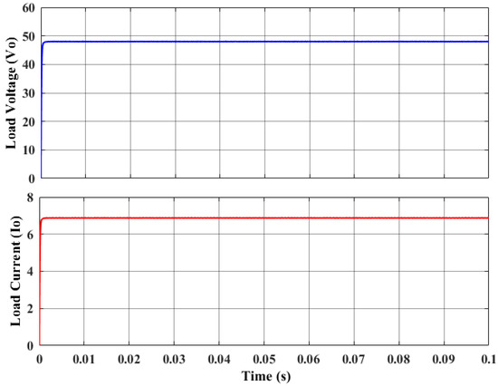
Figure 12.
Load voltage and current waveforms (V0 = 48 V, I0 = 6.875 A).
5.4. Case 4: Performance Analysis of the Converter for a Variable Input Voltage (300–500 Vin) at a Fixed Output Voltage (48 V0) at a Full Load Condition
This section analyzes the performance of the iL2C converter for a variable input voltage of 300–500 Vin at a constant output voltage of 48 V0 under a full load condition. Figure 13 shows that at 0.05 s, the voltage suddenly rose from 300 to 500 Vin; the load voltage and load current waveforms are presented in Figure 14. During the transition of 300–500 Vin, the load voltage and current disturbances occurred at 0.05 s, and magnified figures are also presented. For the steady state voltage and current deviation of +0.4 V (+0.83%) and +0.59 A (+0.85%), a transient voltage and a current dip of +5.2 V (+10.83%) and +7.25 A (+10.54%) were found, respectively, and attained a load voltage of 48 V0 within 1.1 ms.
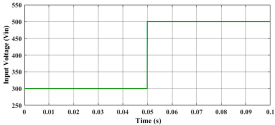
Figure 13.
Variable input voltage waveform (Vin = 300–500 V) at 0.05 s.
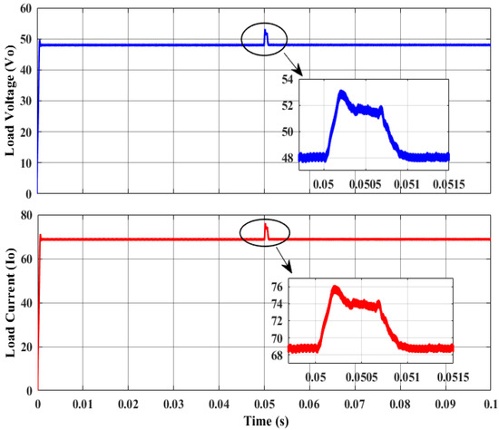
Figure 14.
Step change in load voltage and current waveforms (V0 = 48 V, I0 = 68.75 A).
5.5. Case 5: Performance Analysis of the Converter for a Variable Input Voltage (500–300Vin) at a Fixed Output Voltage (48 V0) at a Full Load Condition
This section analyzes the performance of the iL2C converter for a variable input voltage of 500–300 Vin at a constant output voltage of 48 V0 under a full load condition. Figure 15 shows that at 0.05 the voltage suddenly dropped from 500 to 300 Vin; load voltage and load current waveforms are presented in Figure 16. During the transition of 500–300 Vin, the load voltage and current disturbances occurred at 0.05 s, and magnified figures are also presented. For the steady state voltage and current deviation of +0.42 V (+0.875%) and +0.64 A (+0.93%), a transient voltage and current dip of −3.5 V (−7.29%) and −4.75 A (−6.9%) were found, respectively, and attained a load voltage of 48 V0 within 1.2 ms.
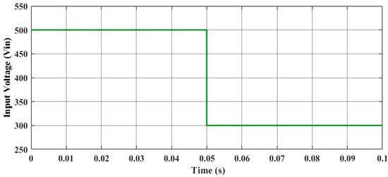
Figure 15.
Variable input voltage waveform (Vin = 500–300 V) at 0.05 s.
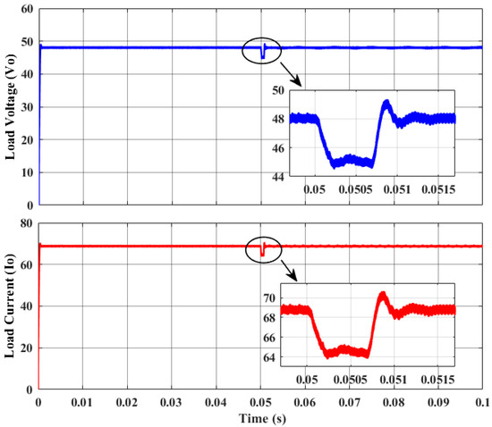
Figure 16.
Step change in load voltage and current waveforms (V0 = 48 V, I0 = 68.75 A).
6. Experimental Analysis
This section describes the experimental validation of the iL2C converter using GaN-HEMT technology at a full load condition of 3.3 kW with a variable input voltage of 300–500 Vin at a load voltage of 48 V0. Eight GaN-HEMT switches were utilized to operate the switching circuit; the parameters of the GaN switch GS66508T are presented in Table 3 and the manufacturer is GaN systems [38,39]. Its features include cooled technology with a lower-junction thermal case resistance at high power applications, lower on-state drain resistance, reverse recovery current, zero reverse recovery losses, well designed gate charge characteristics, and its enhancement mode (E-mode) transistor with better packaging capabilities, among others [40]. TMS320F28335 was used as a digital signal processor as the main controller for the iL2C converter, and the prototype was built as per the modeling parameters discussed in Table 4.
Table 3.
GaN GS66508T parameters (manufactured by GaN Systems).
Table 4.
Practical prototype values of the iL2C resonant FB DC–DC converter.
The hardware representation and experimental setup are presented in Figure 17. From Figure 18, the iL2C converter was validated for 3.3 kW (load voltage 48 V0, load current 68.75 A) at variable load conditions.
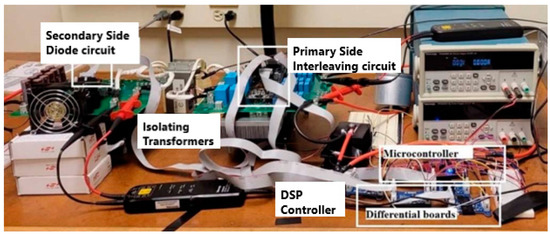
Figure 17.
Test bench setup of the iL2C resonant FB DC–DC converter at 3.3 kW.
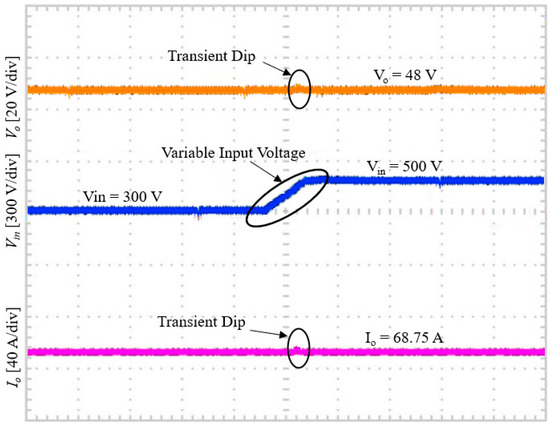
Figure 18.
Experimental waveforms of variable input voltage (Vin = 300–500 V), load voltage, and load current (V0 = 48 V, I0 = 68.75 A).
The results were analyzed at T = 100 ms/div, load voltage = 20 V/div, denoted using a blue line, load current = 50 A/div, denoted using a pink line, and the input source voltage = 300 V/div, denoted using a red line. To perform the dynamic responses at the line side, the sudden change in input voltage occurred at 0.05 s (500 ms) with a small change in load voltage and the current was observed and marked, as shown in Figure 18. It is evident that the converter and controller performed as per the theoretical and simulation analysis. For the steady state voltage and current deviation of +0.76 V (+1.58%) and +1.38 A (+2.0%), a transient voltage and current dip of +6.17 V (+12.85%) and +8.29 A (+12.05%) were found, respectively, and attained a load voltage of 48 V0 within 18 ms.
The efficiency was measured during eight variable load conditions from full load to light load as summarized in Table 5, i.e., 3.3 kW, 3.0 kW, 2.5 kW, 2.0 kW, 1.65 kW, 1.0 kW, 0.5 kW, and 0.33 kW, respectively, when the input and output voltages were 400 Vin and 48 V0. The measured efficiency was 98.2%, 98.7%, and 99.1% at a full load of 3.3 kW, half load of 1.65 kW, and light load of 0.33 kW, respectively. Figure 19 shows the efficiency curve with regard to power.
Table 5.
Efficiency vs. power at 400 Vin with a 48 V0.
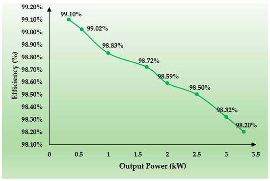
Figure 19.
Efficiency vs. power.
7. Converter Analysis Tables
This section describes the steady state and transient deviations of the voltage and current in various simulated and experimentally analyzed case studies. The values were recorded in tabular format, and Table 6 and Table 7 describe the voltage and current ripple in terms of full load (3.3 kW), half load (1.65 kW), and light load (0.33 kW). Table 8 and Table 9 show the steady state and transient dip and ripples of the voltage and current during variable input voltages from 300 to 500 Vin and 500 to 300 Vin.
Table 6.
Steady state analysis of the load voltage regulation at different load conditions.
Table 7.
Steady state analysis of load current regulation at different load conditions.
Table 8.
Steady state and transient analysis of load voltage during line regulation.
Table 9.
Steady state and transient analysis of load current during line regulation.
From Table 6, the simulations were performed at different load conditions at a rated load voltage of 48 V0 and a source of 400 Vin for examining the load voltage regulation. In case 1, with a minimum voltage ripple of 47.70 V and a maximum voltage ripple of 48.50 V with a load deviation of +0.50 V, the average percentage load voltage ripple was found to be +1.04%. In the next two cases, the minimum voltage ripple and maximum voltage ripple were generated at 47.80 V, 47.94 V and 48.30 V, 48.15 V, respectively. The load deviations occurred at +0.30 V and +0.15 V with an average percentage load voltage ripple of +0.62% and +0.31%, respectively.
Similarly, from Table 7, simulations were performed at different load conditions by maintaining the constant voltages of load 48 V0 and source 400 Vin to examine the load current regulation. In case 1, for a minimum current ripple of 68.30 A and maximum current ripple of 69.40 A with a load deviation of +0.65 A, the average percentage of the load current ripple was found to be +0.94%. In the next two cases, the minimum current ripple and the maximum current ripple were generated at 34.20 A, 6.865 A and 34.55 A, 6.892 A, respectively. The load deviations occurred at +0.175 A and +0.017 A with an average percentage load current ripple of +0.50% and +0.25%, respectively.
From Table 8, simulations were performed to examine the load voltage deviation for variable input voltages, i.e., 300–500 Vin and 500–300 Vin, by maintaining the load voltage at 48 V0 and the load current at 68.75 A, respectively, at full load. In case 4 (300–500 Vin), for a minimum voltage ripple of 47.60 V and maximum voltage ripple of 48.40 V with a load deviation of +0.40 V, the average percentage of load voltage ripple was found to be +0.83%. The transient voltage dip was found to be +5.2 V and its average percentage dip was +10.83%, respectively, with a settling time of 1.1 ms. During case 5 (500–300 Vin), for a minimum voltage ripple of 47.70 V and a maximum voltage ripple of 48.42 V with a load deviation of +0.42 V, the average percentage of the load voltage ripple was found to be +0.875%. The transient voltage dip was found to be −3.5 V and its average percentage dip was −7.29%, respectively, with a settling time of 1.2 ms.
From Table 9, simulations were performed to examine the load current deviation for variable input voltages, i.e., 300–500 Vin and 500–300 Vin, by maintaining the load voltage at 48 V0 and load current at 68.75 A, respectively, at full load. In case 4 (300–500 Vin), for a minimum current ripple of 68.2 A and a maximum current ripple of 69.34 A with a load deviation of +0.59, A the average percentage of load current ripple was found to be +0.85%. The transient current dip was found to be +7.25 A and its average percentage dip was +10.54%, respectively, with a settling time of 1.1 ms. During case 5 (500–300 Vin), for a minimum current ripple of 68.3 A and maximum current ripple of 69.39 A with a load deviation of +0.64 A, the average percentage of the load current ripple was found to be +0.93%. The transient current dip was found to be −4.75 A and its average percentage dip was −6.90%, respectively, with a settling time of 1.2 ms.
Finally, after experimental validation of the iL2C converter’s topology and the VFPSM control technique with a variable input voltage of 300 Vin–500 Vin at a full load of 3.3 kW (V0 = 48 V & I0 = 68.75 A), its use was verified and a comparative table is presented in Table 10 and Table 11 in terms of line regulation for voltage and current at steady state and transient conditions respective to the simulations.
Table 10.
Simulation vs. experimental analysis of load voltage deviations during line regulation from (300–500 Vin).
Table 11.
Simulation vs. experimental analysis of load current deviations during line regulation from (300–500 Vin).
From Table 10, in the case of experimental analysis, for a minimum voltage ripple of 46.50 V and maximum voltage ripple of 48.76 V with a load deviation of +0.76 V, the average percentage of load voltage ripple was found to be +1.58%. The transient voltage dip was found to be +6.17 V and its average percentage dip was +12.85%, respectively, with a settling time of 18 ms.
From Table 11, in the case of experimental analysis, for a minimum current ripple of 68.5 A and maximum voltage ripple of 70.13 A with a load deviation of +1.38 A, the average percentage of the load voltage ripple was found to be +2.00%. The transient voltage dip was found to be +8.29 A and its average percentage dip was +12.05%, respectively, with a settling time of 18 ms.
8. Conclusions
An iL2C Resonant FB DC–DC converter with a hybrid control strategy called the VFPSM technique with a wide input voltage for EV charging systems was investigated.
Firstly, the iL2C converter was modeled and its working principle was demonstrated with the two-converter strategy, which increased the load capacity with a reduction in current ripples. To adapt the wide input voltage, tight regulation, and soft switching, a hybrid control strategy was proposed for the entire operating region, and its control loop design was discussed.
Simulations were conducted using MATLAB/Simulink for the entire proposed design. The converter performance was shifted in different case studies; during case 1, case 2, and case 3, the converter operated at different load conditions, i.e., full load (3.3 kW), half load (1.65 kW), and light load (10% of full load) with a constant input and load voltage of 400–48 V0. The steady-state analysis of load voltage and current regulation was determined with average percentage ripples. The converter’s performance was also examined under assorted input voltage conditions from 300 to 500 Vin in case 4 and 500 to 300 Vin in case 5 at a full load condition. The load voltage and current deviations during line regulation were determined in terms of steady state and transient analysis.
Furthermore, to validate the converter and controller feasibility design, an experimental prototype was built for a 48 V0 charging system with a variable input voltage of 300–500 Vin and implemented by using GaN-HEMT technology with an efficiency of 98.2% at full load. The steady-state and transient analysis of the proposed concept for voltage and current ripples at the load side was discussed.
Author Contributions
Conceptualization, R.P.N.; methodology, R.P.N.; software, R.P.N.; validation, R.P.N.; formal analysis, R.P.N. and S.M.; investigation, R.P.N.; writing—original draft preparation, R.P.N.; writing—review and editing, R.P.N.; supervision, S.M. All authors have read and agreed to the published version of the manuscript.
Funding
This research received no external funding.
Data Availability Statement
Not applicable.
Conflicts of Interest
The authors declare no conflict of interest.
Abbreviations
The abbreviations used in this paper are summarized as follows:
| AC | Alternating Current |
| BEV | Battery Electric Vehicle |
| CV | Constant Voltage |
| DC | Direct Current |
| EMI | Electromagnetic Interference |
| E-mode | Enhancement mode |
| EV | Electric Vehicle |
| FB | Full Bridge |
| FCEV | Fuel cell Electric Vehicle |
| GaN | Gallium nitride |
| HEMT | High Electron Mobility Transistor |
| HEV | Hybrid Electric Vehicle |
| ICE | Internal Combustion Engine |
| iL2C | Interleaved Inductor–inductor–capacitor |
| L2C | Inductor–inductor–capacitor |
| PHEV | Plugin Hybrid Electric Vehicle |
| SCEV | Super Capacitor Electric Vehicle |
| Si | Silicon |
| UCEV | Ultra-Capacitor Electric Vehicle |
| VCO | Voltage Control Oscillator |
| VFPSM | Variable Frequency Phase Shift Modulation |
| ZCS | Zero Current Switching |
| ZVS | Zero Voltage Switching |
References
- Mopidevi, S.; Narasipuram, R.P.; Aemalla, S.R.; Rajan, H. Emobility: Impacts and analysis of future transportation electrification market in economic, renewable energy and infrastructure perspective. Int. J. Powertrains 2022, 11, 264–284. [Google Scholar] [CrossRef]
- Zhou, K.; Wu, Y.; Wu, X.; Sun, Y.; Teng, D.; Liu, Y. Research and development review of power converter topologies and control technology for electric vehicle fast-charging systems. Electronics 2023, 12, 1581. [Google Scholar] [CrossRef]
- Shahjalal, M.; Shams, T.; Tasnim, M.N.; Ahmed, M.R.; Ahsan, M.; Haider, J. A critical review on charging technologies of electric vehicles. Energies 2022, 15, 8239. [Google Scholar] [CrossRef]
- Narasipuram, R.P.; Mopidevi, S. A technological overview & design considerations for developing electric vehicle charging stations. J. Energy Storage 2021, 43, 103225. [Google Scholar]
- Chakraborty, S.; Vu, H.-N.; Hasan, M.M.; Tran, D.-D.; Baghdadi, M.E.; Hegazy, O. DC-DC converter topologies for electric vehicles, plug-in hybrid electric vehicles and fast charging stations: State of the art and future trends. Energies 2019, 12, 1569. [Google Scholar] [CrossRef]
- Raghavendra, K.V.G.; Zeb, K.; Muthusamy, A.; Krishna, T.N.V.; Kumar, S.V.S.V.P.; Kim, D.-H.; Kim, M.-S.; Cho, H.-G.; Kim, H.-J. A comprehensive review of dc–dc converter topologies and modulation strategies with recent advances in solar photovoltaic systems. Electronics 2020, 9, 31. [Google Scholar] [CrossRef]
- Sayed, K.; El-Zohri, E.H.; Mahfouz, H. Analysis and design for interleaved ZCS buck DC-DC converter with low switching losses. Int. J. Power Electron. 2017, 8, 210–231. [Google Scholar] [CrossRef]
- Saleeb, H.; Sayed, K.; Kassem, A.; Mostafa, R. Control and analysis of bidirectional interleaved hybrid converter with coupled inductors for electric vehicle applications. Electr. Eng. 2020, 102, 195–222. [Google Scholar] [CrossRef]
- Lazar, J.F.; Martinelli, R. Steady-state analysis of the LLC series resonant converter. In Proceedings of the Sixteenth Annual IEEE Applied Power Electronics Conference and Exposition, Anaheim, CA, USA, 4–8 March 2001; Volume 2, pp. 728–735. [Google Scholar]
- Bai, H.; Zhang, Y.; Semanson, C.; Luo, C.; Mi, C.C. Modelling design and optimisation of a battery charger for plug-in hybrid electric vehicles. IET Elect. Syst. Transp. 2011, 1, 3–10. [Google Scholar] [CrossRef]
- Deng, J.; Li, S.; Hu, S.; Mi, C.C.; Ma, R. Design methodology of LLC resonant converters for electric vehicle battery chargers. IEEE Trans. Veh. Technol. 2014, 63, 1581–1592. [Google Scholar] [CrossRef]
- Beiranvand, R.; Rashidian, B.; Zolghadri, M.R.; Alavi, S.M.H. A design procedure for optimizing the LLC resonant converter as a wide output range voltage source. IEEE Trans. Power Electron. 2012, 27, 3749–3763. [Google Scholar] [CrossRef]
- Musavi, F.; Craciun, M.; Gautam, D.S.; Eberle, W.; Dunford, W.G. An LLC resonant DC-DC converter for wide output voltage range battery charging applications. IEEE Trans. Power Electron. 2013, 28, 5437–5445. [Google Scholar] [CrossRef]
- Narasipuram, R.P. Analysis, identification, and design of robust control techniques for ultra-lift Luo DC-DC converter powered by fuel cell. Int. J. Comput. Aided Eng. Technol. 2021, 14, 102–129. [Google Scholar] [CrossRef]
- Shi, B.; Yang, F.; Hu, C.; Ouyang, M. Modelling and improvement of oscillation problem in a double-sided LCC compensation network for electric vehicle wireless power transfer. eTransportation 2021, 8, 100108. [Google Scholar] [CrossRef]
- Sun, W.; Xing, Y.; Wu, H. Modified high-efficiency LLC converters with two split resonant branches for wide input-voltage range applications. IEEE Trans. Power Electron. 2017, 33, 7867–7879. [Google Scholar] [CrossRef]
- Kim, B.-C.; Park, K.-B.; Kim, C.-E.; Moon, G.-W. Load sharing characteristic of two-phase interleaved LLC resonant converter with parallel and series input structure. In Proceedings of the Energy Conversion Congress and Exposition (ECCE), San Jose, CA, USA, 20–24 September 2009; pp. 750–753. [Google Scholar]
- Gu, W.-J.; Harada, K. A new method to regulate resonant converters. IEEE Trans. Power Electron. 1988, 3, 430–439. [Google Scholar]
- Ahmad, A.; Khalid, M.; Ullah, Z.; Ahmad, N.; Aljaidi, M.; Malik, F.A.; Manzoor, U. Electric vehicle charging modes, technologies, and applications of smart charging. Energies 2022, 15, 9471. [Google Scholar] [CrossRef]
- Leijon, J.; Boström, C. Charging Electric vehicles today and in the future. World Electr. Veh. J. 2022, 13, 139. [Google Scholar] [CrossRef]
- Guo, B.; Zhang, Y.; Zhang, J.; Gao, J. Hybrid control strategy of phase-shifted full-bridge LLC converter based on digital direct phase-shift control. J. Power Electron. 2018, 18, 802–816. [Google Scholar]
- Yoo, K.-M.; Lee, J.-Y. A 10-kW two-stage isolated/bidirectional dc/dc converter with hybrid-switching technique. IEEE Trans. Ind. Electron. 2013, 60, 2205–2213. [Google Scholar] [CrossRef]
- Park, H.-P.; Jung, J.-H. Power stage and feedback loop design for LLC resonant converter in high switching frequency operation. IEEE Trans. Power Electron. 2017, 32, 7770–7782. [Google Scholar] [CrossRef]
- Narasipuram, R.P. Modelling and simulation of automatic controlled solar input single switch high step-up DC-DC converter with less duty ratio. Int. J. Ind. Electron. Drives 2017, 3, 210–218. [Google Scholar]
- Zhao, L.; Li, H.; Wu, X.; Zhang, J. An improved phase-shifted full-bridge converter with wide-range ZVS and reduced filter requirement. IEEE Trans. Ind. Electron 2018, 65, 2167–2176. [Google Scholar] [CrossRef]
- Long, X.; Chen, D. Small signal modeling of LLC converter with LED load and quasi-resonant controller based active ripple rejection. Energies 2023, 16, 3773. [Google Scholar] [CrossRef]
- Liu, Z.; Li, B.; Lee, F.C.; Li, Q. High-efficiency high-density critical mode rectifier/inverter for wbg-device-based on-board charger. IEEE Trans. Ind. Electron. 2017, 64, 9114–9123. [Google Scholar] [CrossRef]
- Keshmiri, N.; Wang, D.; Agrawal, B.; Hou, R.; Emadi, A. Current status and future trends of GaN HEMTs in electrified transportation. IEEE Access 2020, 8, 70553–70571. [Google Scholar] [CrossRef]
- Musumeci, S.; Barba, V. Gallium Nitride Power Devices in Power Electronics Applications: State of Art and Perspectives. Energies 2023, 16, 3894. [Google Scholar] [CrossRef]
- Sarnago, H.; Lucía, Ó.; Popa, I.O.; Burdío, J.M. Constant-Current Gate Driver for GaN HEMTs Applied to Resonant Power Conversion. Energies 2021, 14, 2377. [Google Scholar] [CrossRef]
- Ma, C.-T. System planning of grid-connected electric vehicle charging stations and key technologies: A review. Energies 2019, 12, 4201. [Google Scholar] [CrossRef]
- Nguyen, D.-D.; Bui, N.-T.; Yukita, K. Design and optimization of three-phase dual-active-bridge converters for electric vehicle charging stations. Energies 2020, 13, 150. [Google Scholar] [CrossRef]
- Musavi, F.; Cracium, M.; Gautam, D.S.; Eberle, W. Control strategies for wide output voltage range LLC resonant DC-DC converters in battery chargers. IEEE Trans. Veh. Technol. 2014, 63, 1117–1125. [Google Scholar] [CrossRef]
- Beiranvand, R.; Rashidian, B.; Zolghadri, M.R.; Alavi, S.M.H. Optimizing the normalized dead-time and maximum switching frequency of a wide-adjustable-range LLC resonant converter. IEEE Trans. Power Electron. 2011, 26, 462–472. [Google Scholar] [CrossRef]
- Shahzad, M.I.; Iqbal, S.; Taib, S. Interleaved LLC converter with cascaded voltage-doubler rectifiers for deeply depleted pev battery charging. IEEE Trans. Transp. Electrif. 2018, 4, 89–98. [Google Scholar] [CrossRef]
- Vu, H.-N.; Choi, W. A novel dual full-bridge LLC resonant converter for CC and CV charges of batteries for electric vehicles. IEEE Trans. Ind. Electron. 2018, 65, 2212–2225. [Google Scholar] [CrossRef]
- Bing, L.; Wenduo, L.; Yan, L.; Lee, F.C.; van Wyk, J.D. Optimal design methodology for LLC resonant converter. In Proceedings of the Twenty-First Annual IEEE Applied Power Electronics Conference and Exposition, Dallas, TX, USA, 19–23 March 2006; pp. 533–538. [Google Scholar]
- Ma, C.-T.; Yao, B.-H. Design and Implementation of an Integrated Control Scheme for GaN-Based Multiple Power Converters. Micromachines 2023, 14, 833. [Google Scholar] [CrossRef] [PubMed]
- Lumbreras, D.; Vilella, M.; Zaragoza, J.; Berbel, N.; Jordà, J.; Collado, A. Effect of the Heat Dissipation System on Hard-Switching GaN-Based Power Converters for Energy Conversion. Energies 2021, 14, 6287. [Google Scholar] [CrossRef]
- Zulauf, G.; Park, S.; Liang, W.; Surakitbovorn, K.N.; Rivas-Davila, J. COSS Losses in 600 V GaN power semiconductors in soft-switched, high- and very-high-frequency power converters. IEEE Trans. Power Electron. 2018, 33, 10748–10763. [Google Scholar] [CrossRef]


Disclaimer/Publisher’s Note: The statements, opinions and data contained in all publications are solely those of the individual author(s) and contributor(s) and not of MDPI and/or the editor(s). MDPI and/or the editor(s) disclaim responsibility for any injury to people or property resulting from any ideas, methods, instructions or products referred to in the content. |
© 2023 by the authors. Licensee MDPI, Basel, Switzerland. This article is an open access article distributed under the terms and conditions of the Creative Commons Attribution (CC BY) license (https://creativecommons.org/licenses/by/4.0/).