Article

High Static Gain DC–DC Double Boost Quadratic Converter

by
Franciéli Lima de Sá
1,*,
Domingo Ruiz-Caballero
2,
Cleiton Dal’Agnol
3,
William Rafhael da Silva
3 and
Samir Ahmad Mussa
3
1
Department of Electrical Engineering, Facvest University Center, Lages 88501-101, Brazil
2
Escuela de Ingeniería Eléctrica, Pontificia Universidad Católica de Valparaíso, Av. Brasil 2147, Valparaíso 2362804, Chile
3
Department of Electrical and Electronic Engineering, Federal University of Santa Catarina, Florianópolis 88040-900, Brazil
*
Author to whom correspondence should be addressed.
Energies 2023, 16(17), 6362; https://doi.org/10.3390/en16176362
Submission received: 25 May 2023 / Revised: 10 July 2023 / Accepted: 28 August 2023 / Published: 1 September 2023

Abstract

:
This paper presents a study of a new topology of a DC–DC converter titled double quadratic boost non-isolated. This converter has high static gain and proposes to reduce the voltage stress on the switches, where the maximum voltage value at each switch is equal to half of the total output voltage. The paper first presents the theoretical analysis of the converter operating in open loop. The objective of the work is the mathematical modeling and control strategy of the converter, as well as validation through closed loop experimental results. In addition, we present the results of practical tests to demonstrate the operation of the converter, such as the experimental static gain curve, the practical efficiency of the converter, and the output voltage control, as well as the capacitor voltage swing control. The authors designed the prototype for 1 kW, with a switching frequency of f s = 50 kHz, with FPGA-based control and modulation.

1. Introduction

Currently, concerns regarding the environment have increased, contributing to the use of new sustainable practices. In the field of power generation, clean and renewable energy sources have become available, and, with this, equipment such as DC–DC converters has been required more frequently. In this regard, renewable power generation has increased the use of DC–DC converters in photovoltaic systems, as presented in [1,2], both grid-connected and off-grid [3,4]. To optimize the use of solar power, it is common to use an MPPT (maximum power point tracking) controller [5]. DC–DC converters are also used in fuel cell, electric vehicle, or hybrid applications, as in [6,7]. These converters are also employed in aeronautics [8], or even in space applications [9], as well as in uninterruptible power systems or battery-powered systems that require the conversion step. Thus, recent research is studying the development of low-cost, high-power-density DC–DC converters for microgeneration applications, as presented in [10]. However, the applications of power converters are not restricted to continuous conduction, as shown by [11], which demonstrates the importance of these power converters.
In general, Several studies can be cited in the literature on topologies of high-gain static DC–DC converters, as shown in [12,13,14], especially as shown in [15], where the author proposed one of the first high-gain static converters. Thus, as technology has advanced, the cost of semiconductors has decreased, making voltage-raising techniques with low-frequency transformers infeasible for numerous everyday applications. In this regard, high-frequency switched transformers have emerged as an alternative for reducing volume and weight [16].
Thus, magnetically coupled isolated converters can easily raise the voltage, depending on the transformation ratio [17]. However, the switches in these structures can be subjected to high voltage spikes due to the energy accumulated in the dispersion inductance, requiring the use of passive or active clamping circuits [18]. With respect to DC–DC non-isolated converters, no transformer is used. Thus, non-isolated converters have lower cost, lower volume, higher efficiency, and simpler topology compared to isolated converters [19].
Therefore, several techniques are currently proposed to increase the gain, and, recently, in the literature, they are classified into five main subsections: switched capacitor, voltage multiplier, switched inductor, magnetic coupling, and multilevel converters [20].
Briefly, the widely known gain lift technique uses the concept of a switched capacitor. Categorized in the literature as switched capacitor [21], ladder cell [22], step-up 1, and step-up 2 [23], theoretically, one can indefinitely increase the output voltage by increasing the number of capacitor–diode pairs. However, in this case, as well as in voltage multiplier converters, the converters require a high number of components and have a high capacitance requirement to minimize peak current in the semiconductors. This technique can be easily implemented in most topologies.
Similar to the principle of the switched capacitor, the switched inductor is another possibility for voltage rise [23,24,25,26]. The latter basically consists of three diodes and two inductors (or also active gain cell that, instead of three diodes, uses two switches). Thus, the inductors are magnetized in parallel and, in the sequence, demagnetized in series, thus promoting the voltage gain increment of the classic DC–DC converters. However, due to the parametric differences found in the implementation, these cells can cause destructive overvoltage in the switches of the converters where they will be inserted, requiring the use of higher-voltage switches or clamping circuits. For this, the inductors must be designed with the same inductance, subject to the same operating conditions [18,27].
In addition to the techniques mentioned above, we can mention the use of differential converters. These converters consist of two converters: a converter with output polarity equal to that of the input (positive group), and another with the opposite polarity of the input (negative group), providing higher voltage gain for the same cyclic ratio and lower voltage in the semiconductors compared to a single stage with the same output voltage. In contrast, the structure has a high number of components [18,28,29,30].
Therefore, one of the alternatives to raise the gain is the connection of two DC–DC converters in cascade, being a simple way to obtain high-voltage gains [31]. This method has the possibility of integration of the components, the quadratic converters being presented in [32] originating a switching cell of the quadratic DC–DC converters subsequently analyzed by the three conduction modes in [33]. This technique makes it possible to unify the switches by replacing one of them with a diode that behaves in earnest with the switch.
In summary, it can be concluded that each voltage boosting technique has its advantages and disadvantages. One attractive alternative for voltage boost is the use of quadratic converters. However, being a high-gain static converter, the topology has the disadvantage of applying the full output bus voltage to its single switch [28]. Thus, in [34], a study was presented to minimize voltage stress and switching losses, whereas, in [35], a three-level quadratic boost converter proposing to reduce the voltage efforts at the switch is presented. However, the modulation technique that must be employed in this topology due to the three-level switching cell naturally promotes a voltage imbalance in the switches for high gains, limiting the application of this converter because of this. Another negative point is that the current switched by the lower switch remains high.
In this context, considering the mentioned information, this work presents a topology that distributes the voltage efforts in the components, eliminating the need for complex modulation techniques and simplifying the dynamic modeling due to the possibility of analyzing only the top half of the topology. In addition, the proposed topology allows the connection of load on both the full bus and half of the bus since it naturally has a midpoint. This further expands the application possibilities of the topology, especially in cases where a midpoint is required [36].
Thus, the theoretical analysis of the proposed topology presents the operating stages and waveforms of the converter operating in continuous, critical, and discontinuous conduction mode. In addition, the mathematical model, as well as experimental tests, for the converter operating in continuous conduction mode is presented. It developed dynamic modeling using a state-space model to obtain the transfer function of voltage and current plants. In addition, it presents the experimental results for the converter in open loop and closed loop. Also of note is the evaluation of the voltage balance of the output capacitors, and such characteristics may not occur naturally with unbalanced load. Thus, the work presents a control strategy aiming to equalize these voltages. Therefore, in summary, the main advantages of this topology are the division of voltage stress, modularity, simplified control, high static conversion efficiency, and simple modulation.

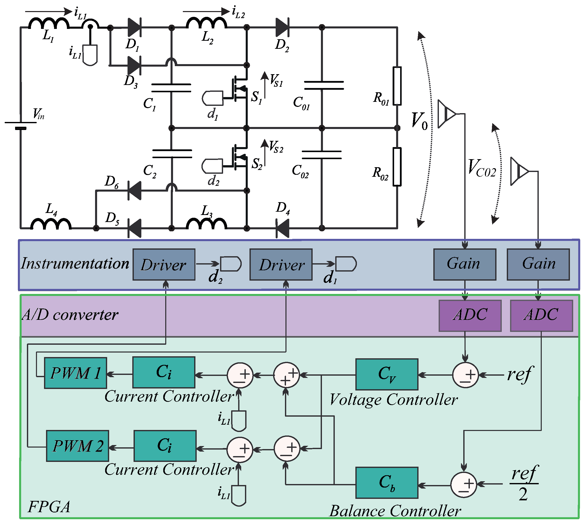
2. Converter Topology

The double quadratic boost converter is characterized by having a high static gain and low voltage efforts in its switches. Figure 1 shows the topology of the proposed converter. In this structure, the voltages on the S 1 and S 2 switches are equal to half of the total output voltage, ( V 0 / 2 ) [37].
An interesting question that simplifies the analysis of this converter is its symmetry since the behavior of the electrical variables in the components of the upper part of the power circuit has the same conduct of the elements in the lower part, so this converter becomes a multiport converter. In this section, we will present the analyses of the converter operating in continuous, critical, and discontinuous conduction modes.

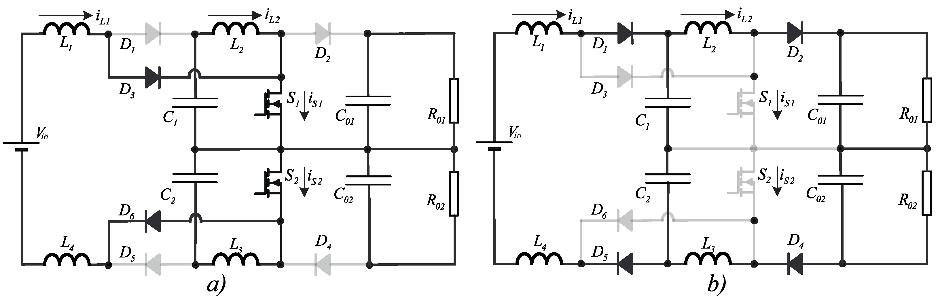
2.1. Operation in Continuous Conduction Mode (CCM)

In this section are shown the analysis of the operating stages, the waveforms, and the static gain curve of the proposed converter for continuous conduction mode6. Figure 2 shows the operating stages of the converter in continuous conduction mode, considering the command pulses of the simultaneous switches and duty cycle of 50 % .

2.1.1. First Stage: ( t 0 , t 1 )

At this stage, the switches S 1 and S 2 are turned ON. The V i n voltage source in series with the L 1 inductor, and the C 1 intermediate capacitor in series with the L 2 inductor, are considered as current sources. The diodes D 2 and D 4 are directly polarized, isolating the output from the input source. The current i S 1 equals the sum of i L 1 with i L 2 , and the current i D 1 is null.

2.1.2. Second Stage: ( t 1 , t 2 )

At this stage the switches S 1 and S 2 are turned OFF. The diodes D 2 and D 4 go into conduction and the current sources I L 1 and I L 2 begin to release power to the output. In this stage, the currents i S 1 and i S 2 are null, i D 1 = I L 1 and i D 2 = I L 2 .
According to the described operating stages, Figure 3a illustrates the waveforms of the converter, with their respective time intervals corresponding to each stage. This figure shows the S 1 and S 2 switch current, which is equal to the sum of the currents in the L 1 and L 2 inductors. The voltage on the switches S 1 and S 2 is equal to the total output voltage divided by two.
For the elaboration of the ideal static gain curve, the source V i n and the inductor L 1 are considered a constant current source I L 1 . The energy applied by the source in a period of operation is given by (1). The energy received by capacitor C 1 in the second stage of the operation is given by (2).
E V i n = V i n . I L 1 . T S
E V C 1 = V C 1 . I L 1 . Δ t 2
Considering the converter an ideal system, in a period of operation, all energy applied by the source V i n is received by the intermediate capacitor C 1 . Thus, solving (1) and (2), supply the ideal static gain for the subcircuit A of the converter, shown in (3).
V C 1 V i n / 2 = 1 1 D
The same analysis is developed for the subcircuit B of the converter, considering the intermediate capacitor voltage C 1 as the input voltage and the capacitor voltage C 01 as the output voltage. Using the superposition principle, for the subcircuits A and B of the proposed converter, according to (3), one obtains the ideal static gain of the double boost quadratic converter as a function of the output voltage by input voltage as (4)
V 0 V i n = 1 1 D 2
Figure 4 shows the ideal static gain as a function of the duty cycle for the double boost quadratic converter compared to the static gain of the conventional boost converter. This comparison shows the high static gain of the proposed converter resulting from the quadratic term in the denominator of the expression (4).
For the actual static gain of the converter, the non-idealities of the components due to copper in the inductor windings are included, according to the analysis shown in [38]. The voltage drops in the semiconductors are considered not relevant for the survey of the converter’s actual static gain curve and are not taken into account. Thus, through the developed analysis, similar to the analysis for the survey of the ideal static gain curve, the real static gain equation is developed, that is, considering in this case the losses in the components, as shown in Equation (5).
V 0 V i n = 1 D . 1 1 + R L R . D 2 2
where ( D = D 1 ).
The authors obtain actual static gain for the various ratios between inductor resistance R L and load resistance R. It is considered the influence of the inductor resistance value on the converter static gain curve, which coincides with the ideal curve when R L = 0 . However, the concern with minimizing the inductor resistance value of the double boost quadratic converter is greater since, for values of R L 0 , the static gain curve has a maximum value. Thus, any duty cycle increment from this maximum point of the curve may bring the output voltage to zero, as shown in Figure 4.
In order to consolidate the study, the proposed topology is compared in relation to the static gain and the voltage efforts in the switches with the topologies present in [34,35]. In this comparison, the static gain is the same for the three topologies compared. However, it is observed that the voltage efforts of the switches are half the value in the proposed topology, thus proving the advantage of the studied converter.

2.1.3. Current Ripple in Inductors L 1 and L 2

Starting from the voltage analysis in the L 1 inductor for the 1st operation stage, analyzing the subcircuit A of the converter, is obtained the current ripple in the L 1 inductor, as shown in Equation (6):
Δ i L 1 = V i . D L 1 . f s
where V i = V i n / 2
Knowing that Δ i L 1 = I max L 1 I min L 1 , it is possible to calculate the maximum and minimum current values on the L 1 inductor. The average output current of the converter subcircuit A (current in the intermediate capacitors ( C 1 and C 2 ) can be called intermediate current I C , given by I C = I D 1 _ a v g :
I D 1 _ a v g = I L 1 _ a v g . Δ t 2
I C = I min L 1 + I max L 1 2 . 1 D
Rewriting the equation regarding the current variation of the Δ i L 1 inductor as a function of the maximum current I max L 1 , it is obtained in (9). Substituting Equation (6) in (9) and Equation (9) in (8), it is obtained:
I max L 1 = Δ i L 1 + I min L 1
I C = 1 2 · I min L 1 + V i . D L 1 . f s + I min L 1 · 1 D
Therefore, the maximum and minimum values of the inductor current L 1 are given as a function of the current of the intermediate capacitor I C :
I max _ min _ L 1 = I C 1 D ± V i . D 2 . L 1 . f s
The analysis of inductor L 1 for inductor L 2 is repeated referring to subcircuit B of the converter. Again, from the analysis of the voltage in the inductor, for the 1st stage of operation, the current ripple in the inductor L 2 is obtained, as shown in Equation (12).
Δ i L 2 = V C 1 . D L 2 . f s
From the current ripple in the inductor Δ i L 2 = I max L 2 I min L 2 , it is possible to calculate the maximum and minimum current values in the inductor L 2 . The average output current I 0 is given by I 0 = I D 2 _ a v g :
I D 2 _ a v g = I L 2 _ a v g . Δ t 2
I 0 = I min L 2 + I max L 2 2 . 1 D
Rewriting the equation for current variation in the Δ i L 2 inductor as a function of the maximum current I max L 2 , it is obtained (15). Substituting Equation (12) in (15), and Equation (15) in (14), it is obtained:
I max L 2 = Δ i L 2 + I min L 2
I 0 = 1 2 . I min L 2 + V C 1 . D L 1 . f s + I min L 2 . 1 D
Therefore, the maximum and minimum values of the inductor current L 2 as a function of the output current I 0 are given by
I max _ min _ L 2 = I 0 1 D ± V C 1 . D 2 . L 2 . f s
Considering that the proposed topology is a series association of boost converters, the inductor L 1 belonging to the first converter has an input voltage V i and at the output a voltage equal to the voltage of the capacitor C 1 . For the second converter of the series association, the voltage at capacitor C 1 is considered as the input voltage, and the voltage at capacitor C 01 is considered as the voltage source at the output. Assuming to be an ideal converter, for the power to be the same at the input and output of the proposed topology, knowing that the voltage of the first converter is lower, the current should be higher. Similarly, considering the higher voltage in the second converter, consequently, the current should be lower. Finally, the lower part of the converter is symmetrical to the upper part mentioned above.

2.1.4. Converter Component Design

Considering the principle of volt-second balance in the inductor and knowing that Equation (11) defines the maximum and minimum values for the L 1 inductor, and still that the current ripple in the inductor is given as shown in Equation (9), the value of the L 1 inductor is calculated by isolating it in Equation (6) and considering the 1st stage of operation of the converter. Again, based on the volt-second balance principle for the L 2 inductor, and considering that Equation (17) defines the maximum and minimum values for the L 2 inductor, the same is calculated by isolating it in Equation (12) and considering the 1st stage of operation of the converter, as shown in Table 1, respectively.
Due to the symmetry of the converter topology, the values of the inductors L 3 and L 4 are given by L 3 = L 2 and L 4 = L 1 . Considering the topology of the symmetrical converter, the other components located in the lower region of the converter will not be present during the design because they have their respective dual dimensions.
After the component design, it is possible to calculate the efforts on the converter components for the continuous conduction mode, as shown in Table 2.
Considering the charge balance in the intermediate capacitor, and also its voltage ripple, the capacitance value is calculated so that the capacitor is charged and discharged linearly at each operating period. Thus, the intermediate capacitor is calculated using the expression presented in Table 1. Similar to the analysis performed for the calculation of the intermediate capacitor, the output capacitor is calculated using the expression shown in Table 1. Finally, the load resistance is calculated using the power expression, as shown in Table 1.

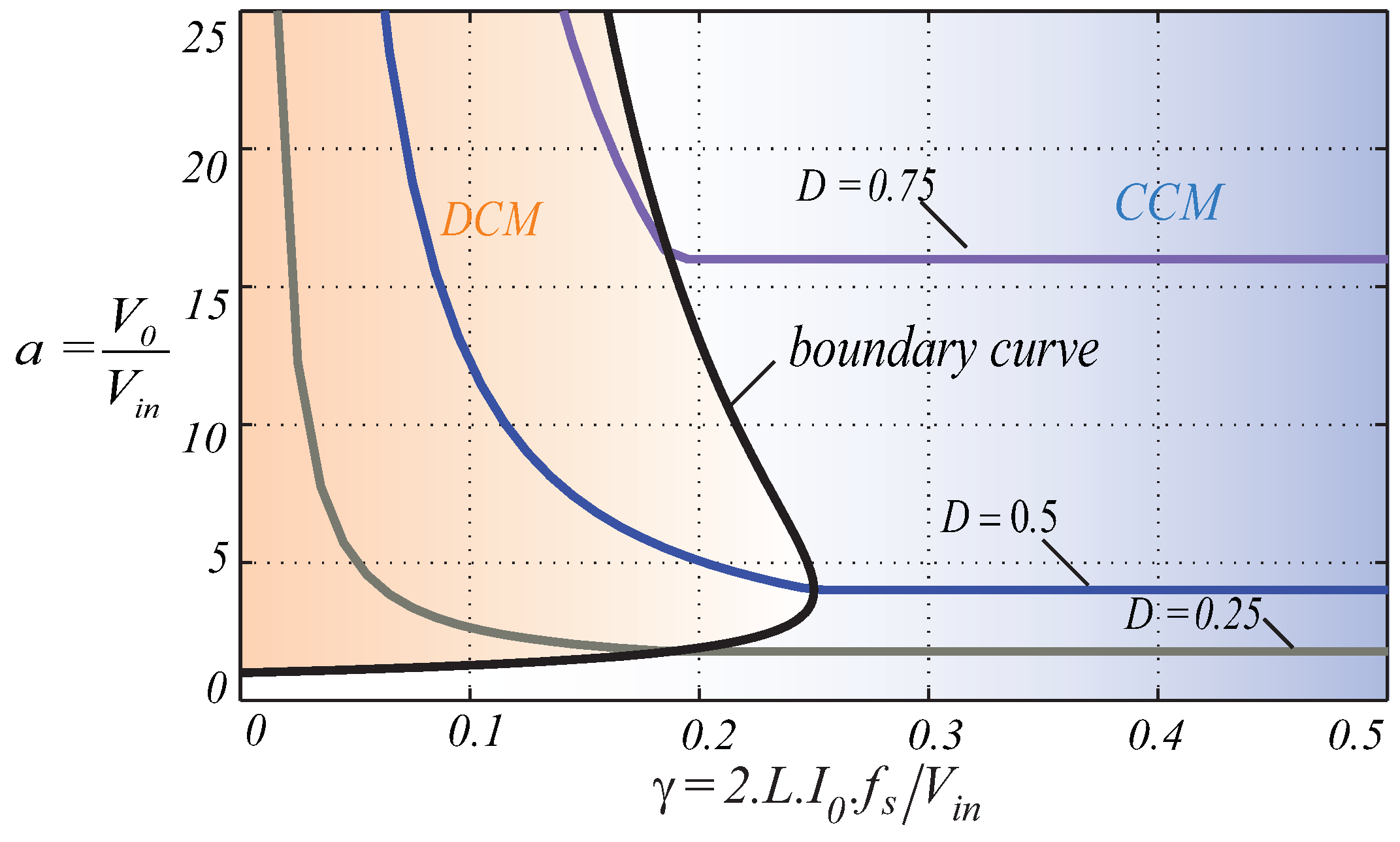
2.2. Operation in Critical Conduction Mode

In this mode of operation, the currents in inductors L 1 and L 2 are initially zero and return to this value precisely at the end of the converter operation period. Figure 3b shows the waveforms of the converter operating in critical conduction mode, with the respective time intervals corresponding to each stage.
The calculation of the critical inductances L 1 and L 2 is developed by analyzing the current ripple in the inductors. The average input current I i n is equal to the average diode current D 1 , and the output current I 0 is the average diode current D 2 .
Through from the maximum and minimum values obtained from the input current I L 1 _ max and I L 1 _ min as a function of capacitor current C 1 for continuous conduction I C , the critical inductance is determined by setting the value of current I L 1 _ min to zero.
L 1 _ C R = V i n 2 . f s . I C . D . 1 D
Repeating the same analysis for the L 2 inductor, given the maximum and minimum values for the input current I L 2 _ max and I L 2 _ min as a function of capacitor output current to the subcircuit B ( I 0 ), in continuous conduction mode, it is determined the critical inductance by setting the value of current I L 2 _ min to zero. In this case, the input voltage becomes the voltage on the intermediate capacitors ( V C ).
L 2 _ C R = V C 2 . f s . I 0 . D . 1 D

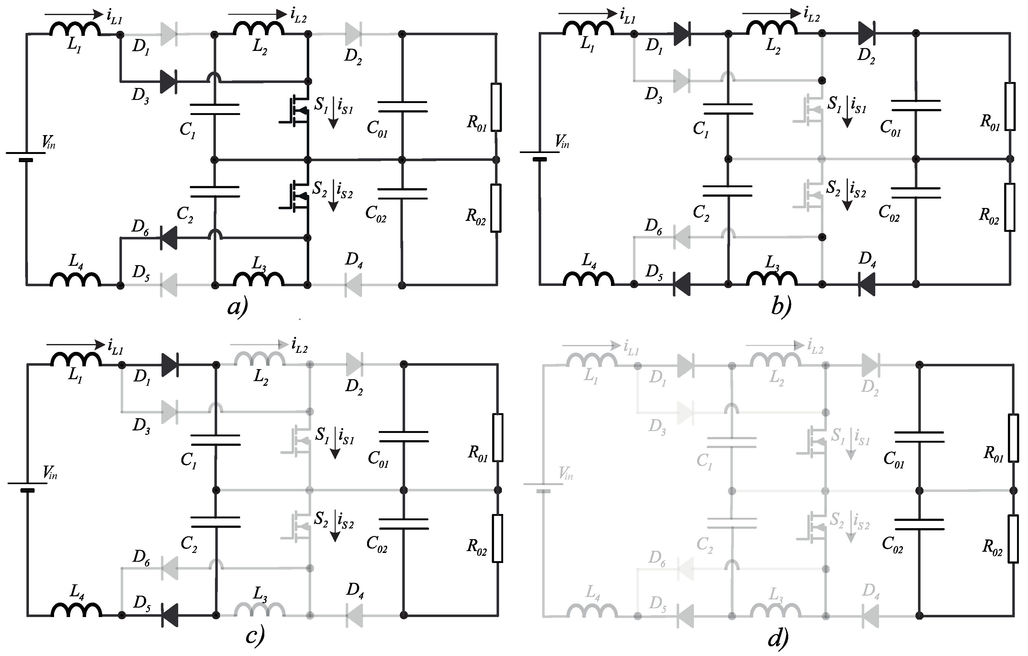
2.3. Operation in Discontinuous Conduction Mode

This converter presents two situations that operate in discontinuous conduction mode. The first occurs when only the current I L 2 is in discontinuous mode, characterized in the third operation stage. Thus, in this situation, the converter operates in the first, second, and third stages of operation.
The second situation presents that the discontinuous conduction mode occurs when the currents I L 1 and I L 2 have discontinuity during the same interval, thus characterizing the fourth stage of operation. Therefore, only in this situation does the converter operate in the first, second, third, and fourth stages.
The following describes the operating stages in discontinuous conduction mode. The first and second operating stages are identical at continuous conduction mode, so they will not be described again.

2.3.1. Third Stage: ( t 2 , t 3 )

This stage transfers all energy stored in L 2 to the load. Therefore, the diode D 2 blocks and the capacitors C 01 and C 02 maintain the voltage of the load. The L 1 inductor continues to supply power to the C 1 and C 2 capacitors.

2.3.2. Fourth Stage: ( t 3 , t 4 )

In this last stage, all energy stored in the L 1 inductor is transferred, and the D 1 diode is blocked. In this stage, only the capacitors C 01 and C 02 feed the load. Figure 5 and Figure 3c show the operating stages and the main waveforms of the converter, respectively. As shown in Figure 3c, the voltage value at switch S 1 in the third and fourth operating stages is equal to half of the total output voltage minus diode voltage D 2 .
To analyze the static gain, in discontinuous conduction mode, the current ripple of inductor L 1 is considered. By analyzing the inductor currents L 1 and diode D 1 for the subcircuit A of the converter as shown in Figure 5, one can obtain (20).
I L 1 _ a v g I D 1 _ a v g = I L 1 _ max 2 . D
Assuming that the input power of the converter is equal to the sum of the powers in the intermediate capacitors, it is shown (21) for the ideal static gain and belonging to the subcircuit A:
V C V i n = 1 + V i n . D 2 2 . I C . L 1 _ D i s . f s
To develop the total ideal static gain of the converter, the superposition principle is used; it is added to Equation (21) for subcircuit A and Equation (23) referring to subcircuit B, obtaining Equation (22). For simplicity, L D i s = L 1 _ D i s = L 2 _ D i s is also considered:
V 0 V i n = 1 + V i n . D 2 2 . I 0 . L D i s . f s 2
In the discontinuous conduction mode, the equations for the design can be obtained through the waveforms in each component of the circuit or by making I m i n L 1 = 0 and I m i n L 2 = 0 in the equations for design in continuous conduction mode.
Repeating the L 1 analysis for the L 2 inductor obtains the ideal static gain equation for subcircuit B:
V 0 V C = 1 + V i n . D 2 2 . I 0 . L 2 _ D i s . f s
To develop the total ideal static gain of the converter, the superposition principle is used; Equation (21) is added for subcircuit A and Equation (23) referring to subcircuit B, obtaining Equation (24). For simplicity, L D i s = L 1 _ D i s = L 2 _ D i s is also considered:
V 0 V i n = 1 + V i n . D 2 2 . I 0 . L D i s . f s 2
In the discontinuous conduction mode, the equations for the design can be obtained through the waveforms in each component of the circuit or by making I m i n L 1 = 0 and I m i n L 2 = 0 in the equations for design in continuous conduction mode.
Figure 6 shows the region for the discontinuous conduction mode, the boundary curve that represents the critical conduction mode, and the region for the continuous conduction mode. In discontinuous conduction mode, the static gain changes when the load is varied. For most practical applications, this is an undesirable way of operating and should be avoided, especially because it causes current stresses in the semiconductors. For this reason, it is very important to operate whenever possible in continuous conduction, where the value of the static gain is constant for a given duty cycle. In this way, the static characteristic curve was surveyed, showing that, for a given duty cycle ratio, the static gain in CCM has a fixed value, while, for DCM, the static gain varies depending on the load.

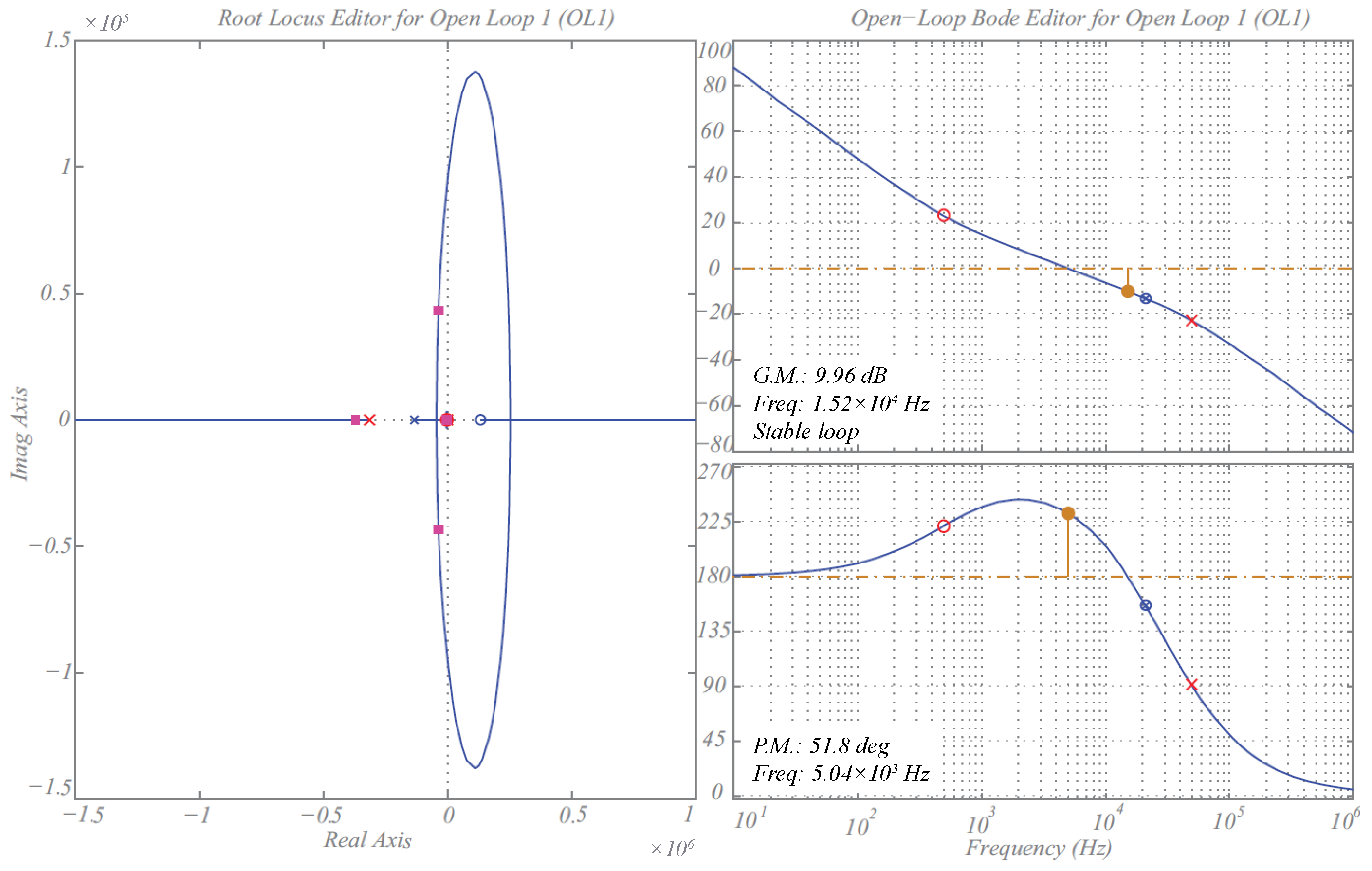
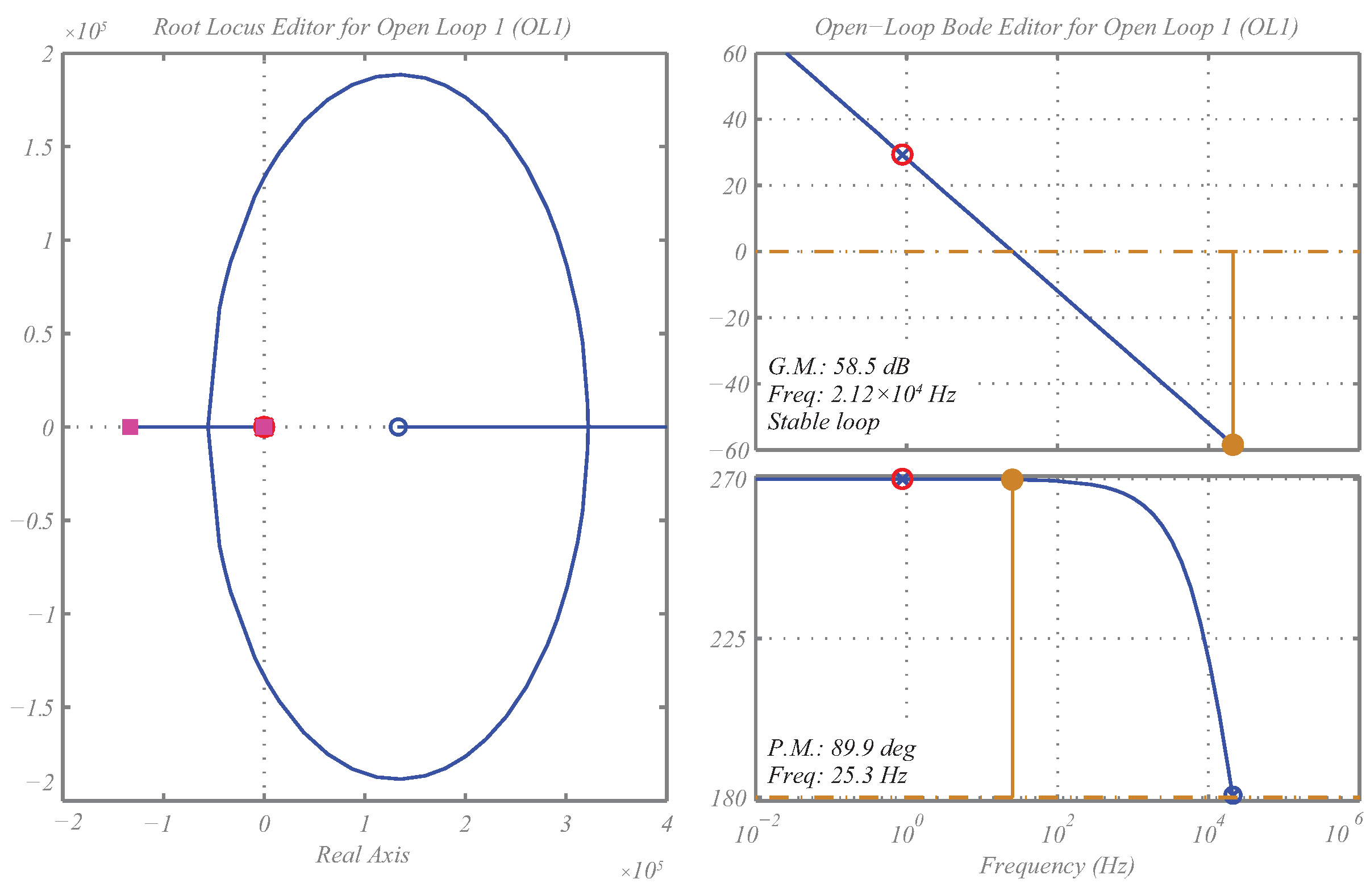
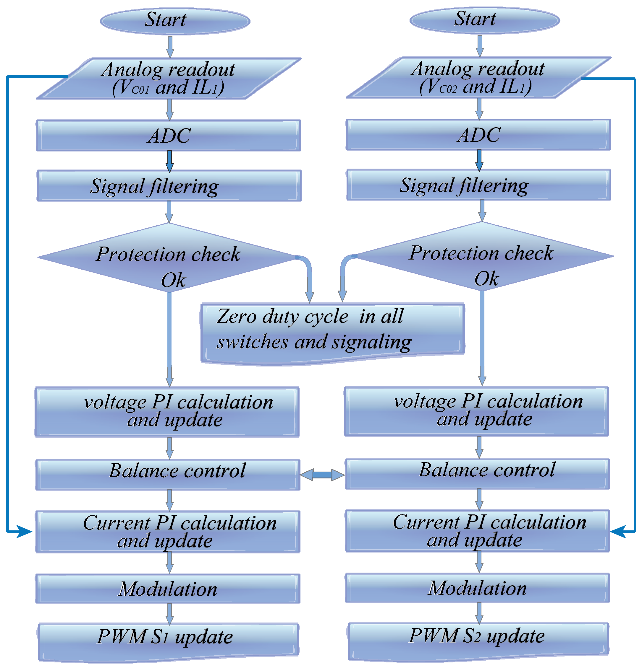
3. Dynamic Modeling and Converter Control

The authors obtained the mathematical model of systems with multiple inputs and outputs employing the state-space modeling, achieving more accurate mathematical models and representing the system precisely, as presented in [38,39]. The system can then be described by input and output equations, as shown in (25).
K x ˙ = A x + B u y = C x
where
x ( a r r a y o f s t a t e s a n d c o n t a i n s = i L 1 ( t ) i L 2 ( t ) V C 1 ( t ) V C 01 ( t ) T ; s t a t e v a r i a b l e s ) K ( m a t r i x t h a t c o n t a i n s t h e e l e m e n t s t h a t = diag ( L 1 , L 2 , C 1 , C 01 ) ; a r e d i r e c t l y l i n k e d t o t h e s t a t e v a r i a b l e s ) u ( s y s t e m i n p u t m a t r i x a n d c o n t a i n s = V i n ( t ) . i n p u t v a r i a b l e s ) A , B , C ( m a t r i c e s t h a t r e l a t e t h e v a r i a b l e s w i t h t h e s y s t e m . )
The dynamic modeling of small signals by the state-space method of the double boost quadratic converter takes into account the operating stages, converter symmetry, and continuous conduction mode, as follows:
First Stage: ( D . T s ) Through the analysis of Figure 2a, one can obtain the state matrix that determines the capacitor voltage and the current in the inductors, as shown in (27).
Second Stage: ( 1 D ) . T s The circuit illustrated in Figure 2b represents the converter operation during this stage, as shown in (27). The C and E arrays vary depending on the choice of output variable.
K x . = A n x + 1 0 0 0 T B n [ V i n ( t ) ] y = I 4 x + E n [ V i n ( t ) ] , n = { 1 , 2 }
where
A 1 = 0 0 0 0 0 0 1 0 0 1 0 0 0 0 0 1 R ; A 2 = 0 0 1 0 0 0 1 1 1 1 0 0 0 1 0 1 R ; I 4 = 1 0 0 0 0 1 0 0 0 0 1 0 0 0 0 1 .
The next step is to obtain the equation that determines the average model of small signals for the two stages of the converter. The average matrix A is given by
A = D A 1 + 1 D A 2
Similarly, we can find the value of matrix B. With the values of the DC components, we can define the small signals of AC model:
K d d t x ^ = A x ^ ( t ) + B u ^ ( t ) + A 1 A 2 X + B 1 B 2 U d ^ ( t )
y ^ = C x ^ ( t ) + E u ^ ( t ) + C 1 C 2 X + E 1 E 2 U d ^ ( t )
where x ^ ( t ) and u ^ ( t ) are small variations on the point of operation and X and U are the values of states and input in steady state. Therefore, considering that the input source has no variation, u ^ ( t ) = 0 , applying the Laplace transform to Equations (29) and (30), and performing the necessary mathematical manipulations, we obtain the transfer function that relates the output to the input.
y ^ ( s ) d ^ ( s ) = C ( s I A ) 1 A 1 A 2 X + B 1 B 2 U + C 1 C 2 X
By obtaining the matrices of the first and second stages of operation, as well as the equations that define the state-space system, the circuit transfer function is accomplished through mathematical software [40]. Through the functions of transferring the input current by the duty cycle and the output voltage by the input current, we obtain the mathematical model of the converter. Therefore, Equation (32) shows the transfer functions of plants to the current and voltage control loops, respectively.
G i L 1 ( s ) = i ^ L 1 ( s ) d ^ ( s ) , G v C 01 ( s ) = v ^ C 01 ( s ) i ^ L 1 ( s )
Moreover, for the converter to be able to reject variations in output voltage and input current peaks at instants of load variations, the controllers in the voltage and current loops are designed, as presented in [41]. For the internal control of the current loop, the linear controller (PI + pole) is used to clear the error in steady state, meeting the following specifications:
The higher the compensator zero, the faster the transient response. However, the phase margin decreases, bringing the system closer to instability. The compensator pole serves to reduce the effect of the switching frequency on the current loop. It is usually positioned at half the switching frequency. Compensator gain is set to ensure the specified zero-crossing frequency (usually limited to a decade below the switching frequency). Equation (33) presents the transfer function current compensator [42]. Figure 7 shows the open loop transfer function (OLTF) design of the inner current loop. The block diagram illustrating the projected loops is shown in Figure 8.
C i ( s ) = k i s + z i s s + p i
where
p i —is positioned at half the switching frequency ( 2 . π . 25 kHz);
z i —is positioned a decade below the crossover frequency, in other words, a decade below the switching frequency ( 2 . π . 500 Hz);
k i —is designed so that the system has a low phase margin (higher than 45 and less than 90 ) at the crossover frequency ( f c r o s s o v e r = f s / 10 ).
Figure 7. OLTF of the internal current loop.
Energies 16 06362 g007
Figure 8. Block diagram representing the internal current loop and the external voltage loop. G c o n v ( s ) represents the complete converter model; v d c is the reference voltage; and i L represents the reference current. The v o and i L variables refer to the converter control variables.
Energies 16 06362 g008
In the design of closed loop control systems, it is often necessary to take a deeper look into the stability issue. The use of Bode diagrams in the analysis of the frequency response of linear systems allows an effective approximation of the frequency response of complex systems. This technique is still widely used for its ease, speed, and amount of information that can be obtained from a given system under analysis in a very simplified way [43]. Therefore, using the definitions:
Gain Margins—This is the gain range that one can increment or decrement the modulus frequency response curve of the open loop (loop) transfer function of a system until the point of critical stability is reached. At this point, the system will still be closed-loop-stable. The gain margin is measured at the frequency where the phase crosses by 180 ° .
Phase Margin—This is the angular value to be added or decreased to the phase curve of the frequency response of a system operating in open loop at the frequency where the modulus curve of the frequency response of this same system has unit value (or 0.0 dB). With this, it ends up indicating how much the phase of the system can be delayed (at the gain crossover frequency) so that the system is still stable in closed loop.
Looking at Figure 7, after controller insertion, if the phase margin is positive, then the system will be stable in closed loop.
For design purposes, the effects of adding controllers and their parameters are more easily visualized in the Bode plot than in the Nyquist plot. Nyquist diagrams are polar diagrams, while Bode diagrams are rectangular diagrams. The Bode diagram is commonly used for control system representation.
For control of the external voltage loop, it adds an integral proportional compensator (PI). In first-order systems, it is usual to position the zero of the compensator PI over the plant pole, canceling it. Thus, the feedback system presents the first-order behavior.
It set the compensator gain to ensure the specified zero-crossing frequency, around 30 Hz. Typically, the voltage loop crossing frequency in DC–DC converters is related to the frequency of the drained pulsed current by the load if an inverter is used as a load. Since this pulsed current is 120 Hz, it defines that the voltage loop crossing frequency is 1 / 4 of the value of this frequency. Equation (34) shows the transfer function of the projected voltage control. Figure 9 shows the open loop transfer function (OLTF) design of the external voltage loop of the converter:
C v ( s ) = k v s + z v s
In addition, for the analysis of the converter, linear systems of non-minimum phase for the direct association with the positioning of poles and finite zeros of the transfer function of the system are considered. For transfer functions that present at least one pole or zero in the right half-plane of the s-plane, the system will be called non-minimal phase [43].
Consider that the model of the converter plant has a zero in the right half-plane of the s-plane. This zero ends up behaving like a pole with respect to the phase response of the system. The open loop transfer function is obtained by multiplying the loop elements. According to the parameters presented in Equation (34), the control Bode diagram is plotted together with the OLTF, presented in Figure 9.
Analyzing Figure 7 and Figure 9, the differences between the plants with respect to gain and phase margin are evident. Thus, the plants will not have the same dynamics; that is, the variations in the inputs will generate different variations in the inputs and will generate different behaviors for each plant.
As shown in Figure 8, in addition to the controllers employed in the current and voltage loops, a discrete control system typically includes a delay resulting basically from the sum of two parcels, the signal sampling delay and the computational delay, totaling in this project a sampling period and a half, represented by e 3 2 T a s .
The internal loop current signal conditioning transfer function, H i ( s ) , equals the association of the current sensor gain ( H s i ), the ADC gain ( H A D C ), and the gain of the instrumentation circuits ( H g i ), as expressed in (35). Voltage conditioning is equivalent, represented by the transfer function H v ( s ) , and given by (35). In the instrumentation circuits, a low pass 1st order filter with cutoff frequency was used, being half of the switching frequency, f c = f s / 2 = 25 kHz.
H x = H s x · H g x · H A D C , x = { v , i }
Finally, the ADC gain is represented by the number of discrete ADC levels divided by the maximum ADC excursion value, in this case given by
H A D C = 2 12 1 A D C max
In the converter model is considered the inclusion of the PWM modulator given by the maximum value of excursion of signal of analogic digital converter ( A D max ) divided by a value representing the peak of the triangular carrier, in others words, dividing the frequency of operation of the FPGA ( f F P G A ) by the sampling frequency, ( f a = 2 f s ) . Equation (37) represents the transfer function of the PWM modulator.
G P W M = A D max 2 f s f F P G A
Due to the converter multiports [44], the studied converter has advantages for application in photovoltaic systems, or in situations where the output voltage bus must be bipolar. In this configuration, it is possible, among others, to reduce the stresses of the switches, making it possible to couple a particular load with total bus voltage by joining two loads, each with half of the total required voltage [45,46].
Thus, when the voltage balance in the output capacitors is necessary, the voltage-balancing technique of these capacitors with a shared loop can be used; that is, the midpoint current can be controlled independently of the input current control. Thus, in addition to full control of the output voltage loop, the system features control of the voltage loop responsible for keeping the midpoint balanced [47]. The technique is based on rejecting slight variations in output voltage so as not to overload one of the capacitors that can assume higher voltage values or total voltage of the bus while the voltage of the other capacitor becomes zero.
The main difference between the loops with separated voltage control and shared voltage control is that the latter use control for the full voltage loop of the converter and a second control for the voltage loop of one of the capacitors to ensure the voltage balance at the midpoint. Figure 10 shows, in block diagram, the voltage balance control of the output capacitors. The blocks presented in the schematic of Figure 10 follow the similar model for the current and voltage loops shown in Figure 8.
The technique with shared voltage control loops has as its primary function to quickly correct the load disturbance at the transient instant. For this, the characteristic is used that the total output voltage does not present high ripples. Therefore, the voltage loop that regulates the midpoint between the output capacitors must have relatively slow dynamics, and with a cut-off frequency much lower than the cut-off frequency of voltage control with separate loops.
The transfer function required for midpoint voltage control is obtained through the state-space model by analyzing (27) for the first and second operating stages. When the converter has its load balanced, its midpoint current is zero. However, when the load is unbalanced, the midpoint current is responsible for the output voltage balance.

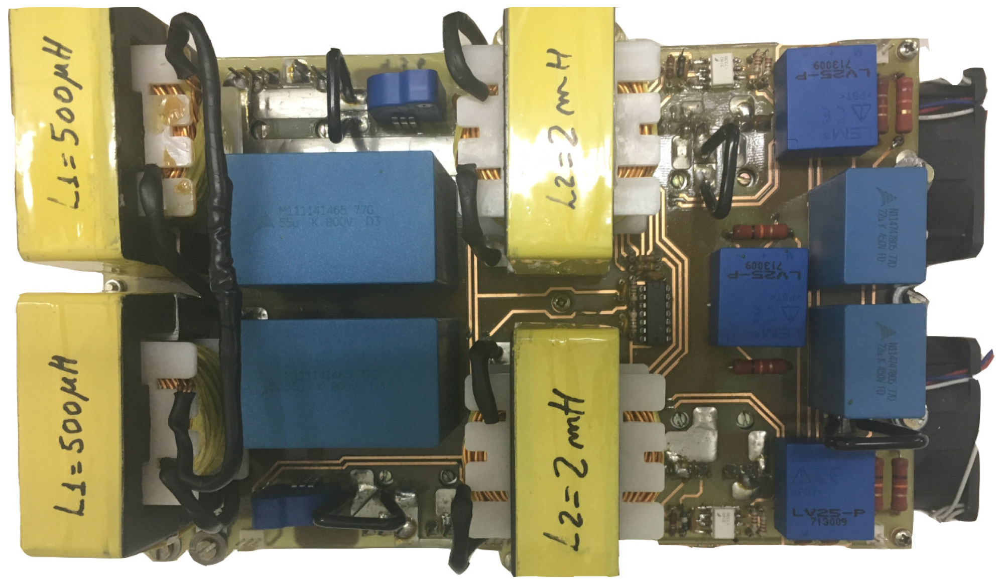
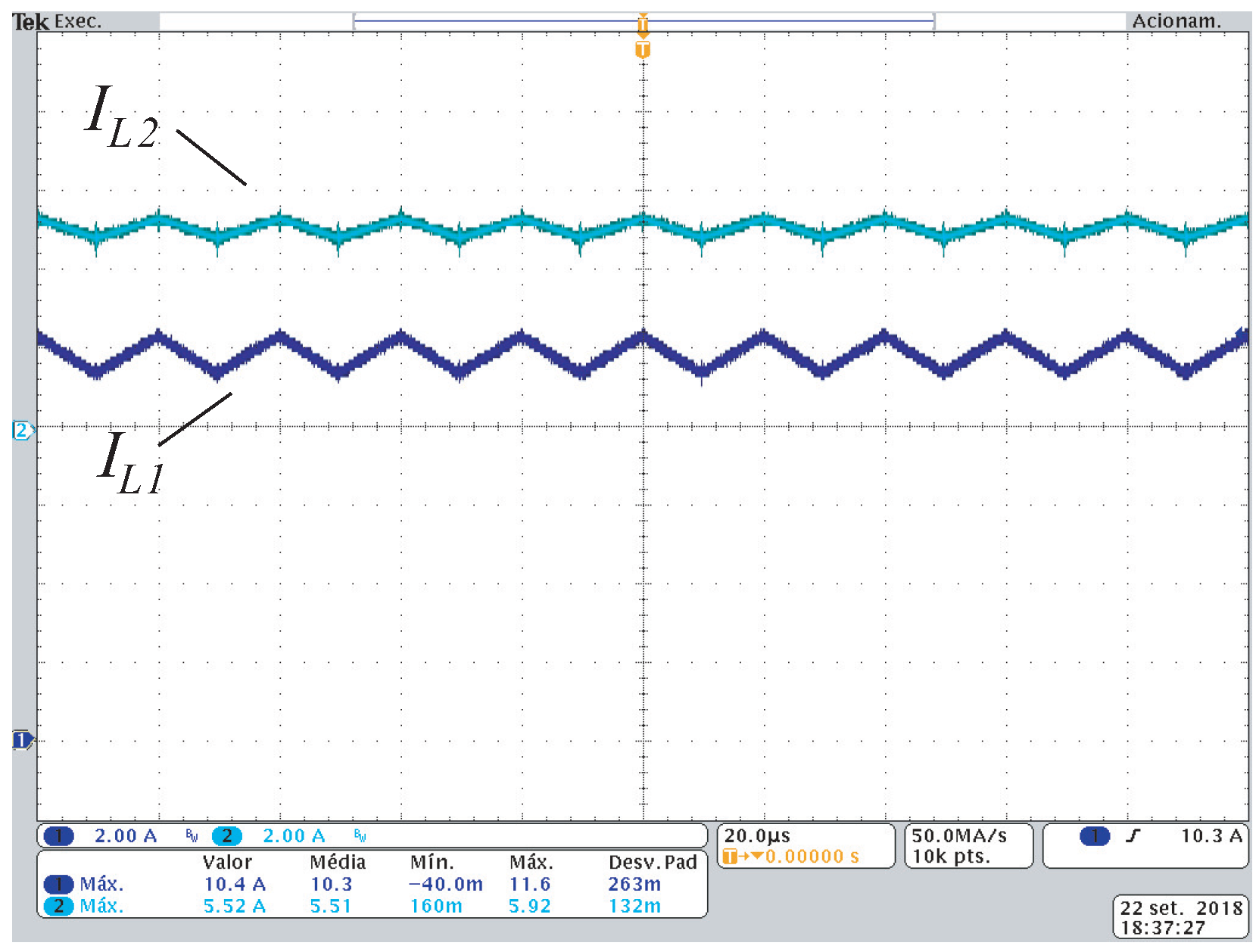
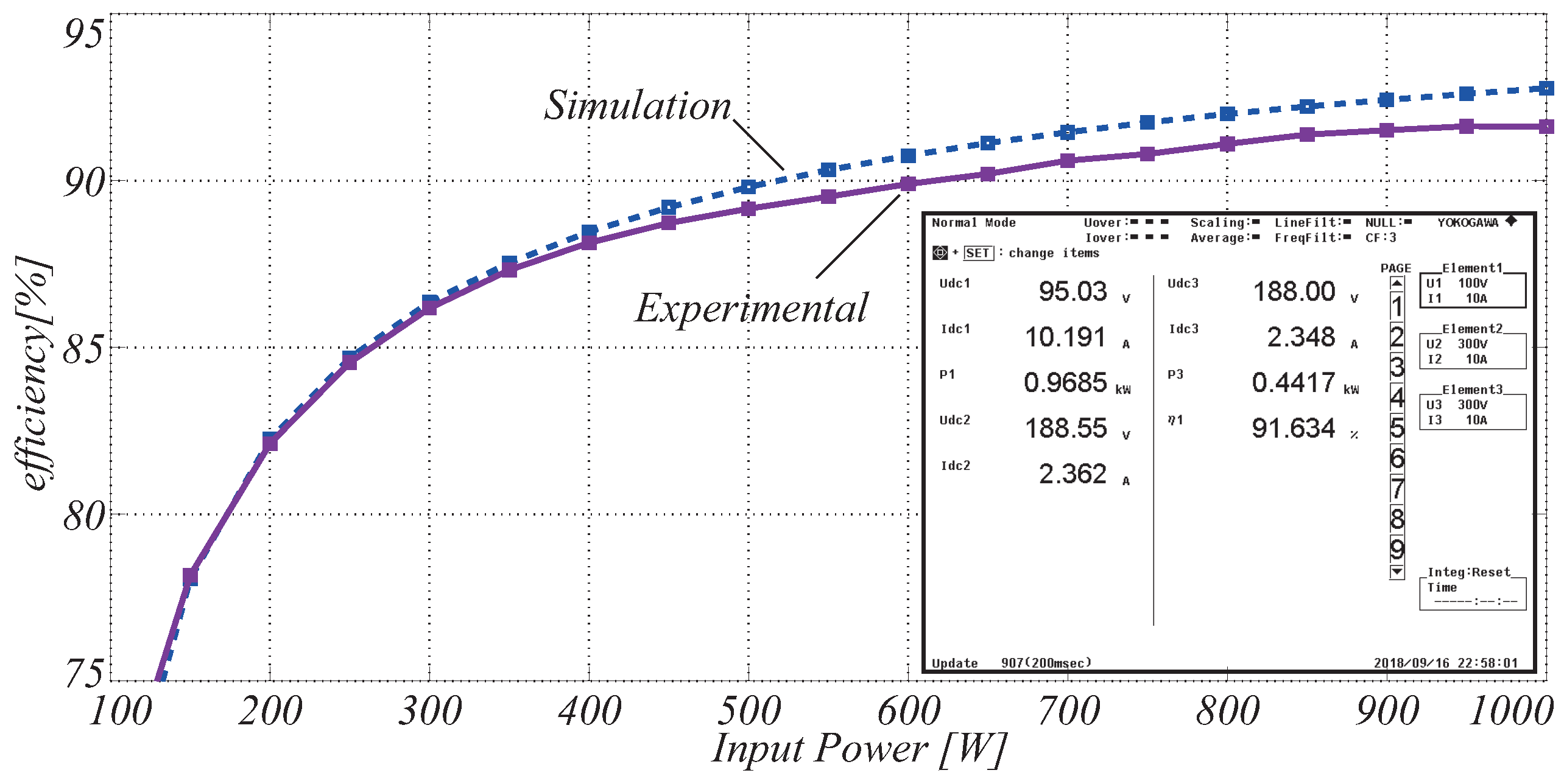
4. Experimental Results

In this section, the authors present the experimental results of the double boost quadratic converter. Table 3 shows the parameters and values of the components used in the implementation of the converter. Laboratory tests were performed with a 1 kW power prototype, as shown in Figure 11. The current and voltage sensor models used were the LTSR-25-NP and the LV-25NP from LEM.
In the development of the experimental tests, the Altera development kit, model BeMicro Max 10, was used [48]. This kit features a 10M08DAF484 FPGA chip, which contains an intrinsic ADC block with 18 channels and 12 bits resolution with up to 1 MHz sampling rate. Converter digital control has been implemented in the FPGA employing the VHDL hardware description language VHSIC HDL (very high-speed integrated circuit hardware description language).
The FPGA has some advantages, such as the real-time processing feature and high processing density; in addition, it is different from microcontrollers because it has a large number of PWM outputs, but the main difference is the parallel processing feature; in other words, it is possible to process digital signals simultaneously without interaction with other processes [48,49]. The flowchart in Figure 12 shows the parallel processing adopted for the control of the double quadratic boost converter. Each block represents a code responsible for generating the hardware description. Thus, several processes with distinct functions work simultaneously.
In this work, the FPGA completes the acquisition, filtering, and processing of data, in addition to modulation and protection of the circuit. As presented in Figure 12, the hardware description was divided and organized into different logic blocks interconnected by a flag responsible for synchronism. Data collection happens when there is no switching in order to avoid noise. Subsequently, the reading data are filtered and sent to the control loop. Finally, they are available for use in the logic block responsible for modulation.

4.1. Converter Operating Open Loop

Figure 13a shows input and output voltages, and, in Figure 13b, it is observed that the voltage at the switches is halved compared to similar topologies in the literature [34].
Comparing the experimental waveforms of the total output voltage V 0 and the input voltage V i n , it verifies the high static gain of the converter (four times for D = 0.5 ). Although the experimental results are presented only for the total output voltage V 0 , these results can be obtained by summing the voltage of the output capacitors V C 01 and V C 02 .
The current in the inductors is significant in the analysis of the converter operating mode. However, it developed the theoretical analysis for continuous, critical, and discontinuous conduction modes; the practical implementation was performed only in continuous driving mode, where these converters generally operate in most applications because of its presented lower current peaks in their semiconductors. The currents in the L 1 and L 2 inductors are shown in Figure 14. The current ripple in the L 1 inductor is greater than in the L 2 inductor, as designed. The project considered a ripple of 10 % in the value of their respective nominal currents.
Converter efficiency is an important parameter and must be taken into consideration. Therefore, Figure 15 presents the comparison of the converter performance obtained via simulation in PSIM using the Device Database Editor tool through the semiconductor models specified in Table 3 and the efficiency obtained through the experimental tests; in this case, the power analyzer Yokogawa wt500 was used. Therefore, it is observed in Figure 15 that the proposed converter has high efficiency, when compared to similar converters found in the literature [50], proven through simulation and experimental tests.
Moreover, as presented in the theoretical analysis through Equations (4) and (5), the double boost quadratic converter has a high static gain. Figure 16 shows the static gain curve obtained by simulation using the Matlab software compared to the experimental curve. For the experimental tests, it was possible to vary the duty cycle D (0–0.85). This value was limited by the power at which the converter was designed and built, according to Table 3. It chose low power value, allowing for a greater range of the duty cycle.
As shown in Figure 16, the static converter gain reached the ratio of 12 times output voltage to the input voltage, as proposed in the theoretical analysis. For the tests, limiting the input inductor current i L 1 occurred in the function of the design current. It performed the test at 15% of the rated power of the converter.

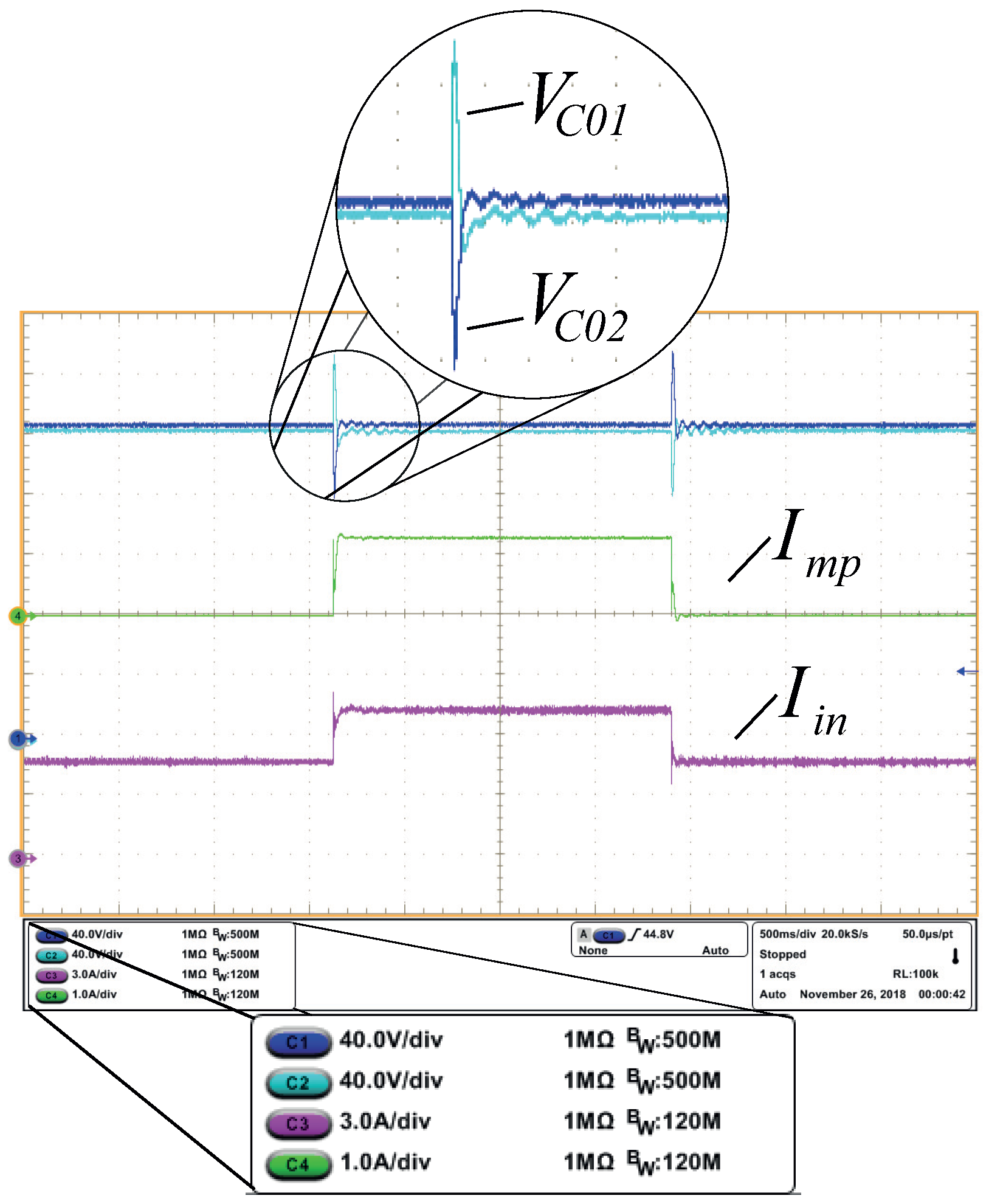
4.2. Converter Operating in Closed Loop
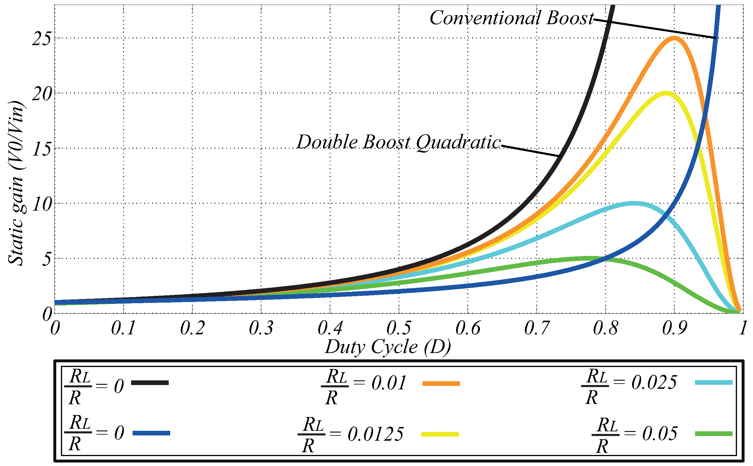
Considering the converter operating in the closed loop with current, voltage, and voltage balance control on the output capacitors, Figure 17 presents the input current, midpoint current, and output capacitor voltages. It develops the tests for a load step of 50% of rated power to 75% of rated power. It noticed that, at the moment of load variation to the input, the current increase ( I i n ) is proportional to the power variation, as shown in Figure 17, and, in this case, the overshoot of one of the output capacitors is similar but with the opposite signal, characterizing their balance control.
In order to complement the load variation test shown in Figure 17, Figure 18a presents the same waveforms, replacing the input current with the total output voltage. In this case, despite the variation in the input current shown in Figure 17, there is no variation in the output capacitor voltage V C 01 and V C 02 , just a small overshoot at the time the load steps occurred.
In Figure 18a, it is noticed that the overvoltage at the V 0 total voltage is lower when compared to the overvoltage at the output capacitors V C 01 and V C 02 , proving that the balance control can balance the voltage values in the capacitors, even with load imbalance. To keep the voltage on the output capacitors unchanged despite load imbalance, the midpoint current I m p is responsible for absorbing this imbalance through this current variation.
In order to introduce the operation of the converter against the imbalances in the output capacitor voltages, besides the load variation, Figure 18b presents the midpoint current, the output capacitor voltages, and the total output voltage at four different times: (a) in t 1 load imbalance ( R 01 ); (b) in t 2 total load disturbance ( 50 % ); (c) in t 3 load disturbance (removal of 50% total load); and (d) in t 4 removal of load imbalance ( R 01 ).

5. Discussion

For the converter operating in open loop, the input and output voltage ratio of the converter in the experimental results proves the high static gain of the proposed topology. Observing also the experimental curves of the voltages in the switches, it can be proved that they have half the value of the total bus voltage, which characterizes a great advantage of this converter. Furthermore, by analyzing the converter in a closed loop, the relationship between the inductor currents L 1 and L 2 is provided by a factor k = 2 . As it is a voltage step-up converter, the current ripple at L 1 is greater than the current ripple at inductor L 2 . Furthermore, the voltages in the intermediate capacitors V C 1 and V C 2 are proportional to the voltages in the output capacitors V C 01 and V C 02 . Finally, since these are open loop results, the current at the midpoint of the converter is zero since, in this case, the loads are balanced.
For the converter operating in closed loop, the experimental results show that the current and voltage control present better behaved curves when compared to only the voltage control. This is because inserting input current control in addition to output voltage control produces a more accurate response, as expected.
In cases where the loads are unbalanced and, consequently, the current at the midpoint of the converter has a non-zero average value, it is interesting to insert the output capacitors voltage balance control. This control has a good response to moments of load unbalance and total load variation. While the total output voltage remains unchanged, the voltages on the output capacitors are proportionally changed at these times. Finally, the neutral current undergoes full value variation only at moments of load unbalance; at moments of load variation, only small current peaks are observed, as expected.

6. Conclusions

Considering that energy generation is fundamental for world economic development, combined with care for the environment and sustainable practices, the generation of energy through renewable sources plays an important role. Thus, research related to applications in the field of electricity is fundamental to technological development.
Therefore, considering optimizing power converters for these applications, in this work, the study of a new non-isolated high static gain converter DC–DC was presented. The operating stages and waveforms of the converter have been shown for continuous, critical, and discontinuous conduction mode in addition to the ideal static gain curves, actual static gain for the various load resistance values, and the curve representing the boundary between the conduction modes. For the development of the dynamic mathematical model, the state-space technique was used.
Due to the symmetry of the converter, it was possible to reduce the stresses on the switches. Moreover, its symmetry also simplified its mathematical model, as presented in the paper, in which an eighth-order system can be simplified by a fourth-order system, making it easier to obtain its transfer function. In this configuration, this converter can be used, for example, in conjunction with a multilevel inverter coupled to its output for photovoltaic generation, grid-connected applications, or coupled to AC loads requiring low harmonic distortion rates.
The experimental results were presented, confirming the theoretical analysis. Thus, it was possible to verify the high static gain (greater than twelve times) experimentally through the practical tests of the duty cycle variation, where the results were obtained as expected. Also, it was possible to verify the reduced voltage efforts on the converter switches when compared to existing converters in the literature [34,35]. Although mirroring the converter proposed in the paper makes it dual, the purpose of this mirroring is not to increase their power processing capacity but to decrease the voltages at their switches. However, the switch of the Quadratic Boost Converter [34,35] must support the full bus voltage, while, in the proposed converter, the switches will support only half of the bus voltage.
As it is an important parameter, the efficiency curve of the converter was presented in the experimental results, proving the high efficiency of the proposed converter. Finally, the results show that this converter has great natural potential for application in renewable energies, thus being an excellent option in the conditioning of power generation through photovoltaic panels.

Author Contributions

Conceptualization, D.R.-C. and S.A.M.; methodology, S.A.M.; software, F.L.d.S.; validation, F.L.d.S.; formal analysis, F.L.d.S.; investigation, F.L.d.S. and C.D.; resources, F.L.d.S. and C.D.; data curation, F.L.d.S.; writing—original draft preparation, F.L.d.S. and C.D.; writing—review and editing, F.L.d.S. and W.R.d.S.; visualization, F.L.d.S. and W.R.d.S.; supervision, S.A.M.; project administration, S.A.M. All authors have read and agreed to the published version of the manuscript.

Funding

This research received no external funding.

Data Availability Statement

Data sharing is not applicable to this article.

Acknowledgments

We would like to thank the Institute of Power Electronics, INEP—UFSC, for the equipment and laboratory provided for the development of practical experiments.

Conflicts of Interest

The authors declare no conflict of interest.

References

  1. Danielis, R.; Scorrano, M.; Massi Pavan, A.; Blasuttigh, N. Simulating the Diffusion of Residential Rooftop Photovoltaic, Battery Storage Systems and Electric Cars in Italy. An Exploratory Study Combining a Discrete Choice and Agent-Based Modelling Approach. Enegies 2023, 16, 557. [Google Scholar] [CrossRef]
  2. Sumathy, P.; Navamani, J.D.; Lavanya, A.; Sathik, J.; Zahira, R.; Essa, F.A. PV Powered High Voltage Pulse Converter with Switching Cells for Food Processing Application. Energies 2023, 16, 1010. [Google Scholar] [CrossRef]
  3. Karbowniczak, A.; Latała, H.; Ne˛cka, K.; Kurpaska, S.; Książek, L. Modelling of Energy Storage System from Photoelectric Conversion in a Phase Change Battery. Energies 2022, 15, 1132. [Google Scholar] [CrossRef]
  4. Kishore, P.M.; Bhimasingu, R. Dual-input and triple-output boost hybrid converter suitable for grid-connected renewable energy sources. IET Power Electron. 2020, 13, 808–820. [Google Scholar] [CrossRef]
  5. Khodair, D.; Motahhir, S.; Mostafa, H.H.; Shaker, A.; Munim, H.A.E.; Abouelatta, M.; Saeed, A. Modeling and Simulation of Modified MPPT Techniques under Varying Operating Climatic Conditions. Energies 2023, 16, 549. [Google Scholar] [CrossRef]
  6. Pellitteri, F.; Di Dio, V.; Puccio, C.; Miceli, R. A Model of DC-DC Converter with Switched-Capacitor Structure for Electric Vehicle Applications. Energies 2022, 15, 1224. [Google Scholar] [CrossRef]
  7. Yalla, N.; Agarwal, P.; Venkata, J.S.P.A.; Bussa, V.K. Reduced switching state multilevel improved power factor converter for level-3 electric vehicle applications. IET Power Electron. 2020, 13, 693–702. [Google Scholar] [CrossRef]
  8. Russo, A.; Cavallo, A. Stability and Control for Buck–Boost Converter for Aeronautic Power Management. Energies 2023, 16, 988. [Google Scholar] [CrossRef]
  9. Li, H.; Gu, Y.; Zhang, X.; Liu, Z.; Zhang, L.; Zeng, Y. A Fault-Tolerant Strategy for Three-Level Flying-Capacitor DC/DC Converter in Spacecraft Power System. Energies 2023, 16, 556. [Google Scholar] [CrossRef]
  10. Zhou, G.; Tian, Q.; Leng, M.; Fan, X.; Bi, Q. Energy management and control strategy for DC microgrid based on DMPPT technique. IET Power Electron. 2020, 13, 658–668. [Google Scholar] [CrossRef]
  11. Kumar, R.; Wu, C.-C.; Liu, C.-Y.; Hsiao, Y.-L.; Chieng, W.-H.; Chang, E.-Y. Discontinuous Current Mode Modeling and Zero Current Switching of Flyback Converter. Energies 2021, 14, 5996. [Google Scholar] [CrossRef]
  12. Farakhor, A.; Abapour, M.; Sabahi, M. Study on the derivation of the continuous input current high-voltage gain DC/DC converters. IET Power Electron. 2018, 11, 1–9. [Google Scholar] [CrossRef]
  13. Sedaghati, F.; Pourfajar, S. Analysis and implementation of a boost DC-DC converter with high voltage gain and continuous input current. IET Power Electron. 2020, 13, 798–807. [Google Scholar] [CrossRef]
  14. Samuel, V.J.; Keerthi, G.; Mahalingam, P. Coupled inductor-based DC-DC converter with high voltage conversion ratio and smooth input current. IET Power Electron. 2020, 13, 733–743. [Google Scholar] [CrossRef]
  15. Middlebrook, R.D. Transformerless DC-to-DC converters with large conversion ratios. IET Power Electron. 1988, 3, 484–488. [Google Scholar] [CrossRef]
  16. Zhao, B.; Song, Q.; Liu, W.; Sun, Y. Overview of Dual-Active-Bridge Isolated Bidirectional DC-DC Converter for High-Frequency-Link Power-Conversion System. IET Power Electron. 2014, 29, 4091–4106. [Google Scholar] [CrossRef]
  17. Jeferson, F. Conversor CC-CC Híbrido Isolado Para Utilização em Sistemas MVDC. Ph.D. Thesis, Universidade Federal de Santa Catarina, Florianópolis, Brazil, 2020. [Google Scholar]
  18. Jéssika Melo de, A. Conversores CC-CC Não-Isolados Elevadores Baseados na Conexão Diferencial de Conversores Com Tensão de Saída de Mesma Polaridade. Ph.D. Thesis, Universidade Federal de Santa Catarina, Florianópolis, Brazil, 2022. [Google Scholar]
  19. Jamshidpour, E.; Poure, P.; Saadate, S. Unified Switch Fault Detection for Cascaded Non-Isolated DC-DC Converters. In Proceedings of the 2018 IEEE International Conference on Environment and Electrical Engineering and 2018 IEEE Industrial and Commercial Power Systems Europe (EEEIC/I&CPS Europe), Palermo, Italy, 12–15 June 2018; pp. 1–5. [Google Scholar] [CrossRef]
  20. Forouzesh, M.; Siwakoti, Y.P.; Gorji, S.A.; Blaabjerg, F.; Lehman, B. Step-Up DC-DC Converters: A Comprehensive Review of Voltage-Boosting Techniques, Topologies, and Applications. IET Power Electron. 2017, 32, 9143–9178. [Google Scholar] [CrossRef]
  21. Zhang, Y.; Zhou, L.; Sumner, M.; Wang, P. Single-Switch, Wide Voltage-Gain Range, Boost DC-DC Converter for Fuel Cell Vehicles. IEEE Trans. Veh. Technol. 2018, 67, 134–145. [Google Scholar] [CrossRef]
  22. Julio Cesar, D. Família de Retificadores Boost Unidirecionais Híbridos Monofásicos Com Célula de Capacitor Chaveado. Ph.D. Thesis, Universidade Federal de Santa Catarina, Florianópolis, Brazil, 2017. [Google Scholar]
  23. Axelrod, B.; Berkovich, Y.; Ioinovici, A. Switched-Capacitor/Switched-Inductor Structures for Getting Transformerless Hybrid DC-DC PWM Converters. IEEE Trans. Circuits Syst. I Regul. Pap. 2008, 55, 687–696. [Google Scholar] [CrossRef]
  24. Fardahar, S.M.; Sabahi, M. New Expandable Switched-Capacitor/Switched-Inductor High-Voltage Conversion Ratio Bidirectional DC-DC Converter. IEEE Trans. Power Electron. 2020, 35, 2480–2487. [Google Scholar] [CrossRef]
  25. Liu, H.; Li, F. A Novel High Step-up Converter with a Quasi-active Switched-Inductor Structure for Renewable Energy Systems. IEEE Trans. Power Electron. 2016, 31, 5030–5039. [Google Scholar] [CrossRef]
  26. Samiullah, M.; Iqbal, A.; Ashraf, I.; Maroti, P.K. Voltage Lift Switched Inductor Double Leg Converter with Extended Duty Ratio for DC Microgrid Application. IEEE Access 2021, 9, 85310–85325. [Google Scholar] [CrossRef]
  27. Lenon, S. Metodologia Para Concepção de Conversores CC-CC de Alto Ganho Baseados em Topologias Básicas Com Indutor Acoplado e Células Multiplicadoras de Tensão. Ph.D. Thesis, Universidade Federal de Santa Catarina, Florianópolis, Brazil, 2020. [Google Scholar]
  28. Wu, T.-F.; Yu, T.-H. Unified approach to developing single-stage power converters. IEEE Trans. Aerosp. Electron. Syst. 1998, 34, 211–223. [Google Scholar] [CrossRef]
  29. de Azevedo Ayres, W.; Bridi, É.; Sartori, H.C.; Pinheiro, J.R. Conversor de Alto Ganho de Tensão Dual Boost Quadrático; SEPOC: Santa Maria, Brasil, 2018. [Google Scholar]
  30. Marcos Antônio, S. Metodologia Aplicada à Derivação e Modelagem de Conversores CC-CC Diferenciais de Alto Ganho. Ph.D. Thesis, Universidade Federal de Santa Catarina, Florianópolis, Brazil, 2020. [Google Scholar]
  31. Matsuo, H.; Harada, K. The Cascade Connection of Switching Regulators. IEEE Trans. Ind. Appl. 1976, IA-12, 192–198. [Google Scholar] [CrossRef]
  32. Maksimovic, D.; Cuk, S. General properties and synthesis of PWM DC-to-DC converters. In Proceedings of the 20th Annual IEEE Power Electronics Specialists Conference, PESC’89 Record, Milwaukee, WI, USA, 26–29 June 1989; Volume 2, pp. 515–525. [Google Scholar]
  33. Maksimovic, D.; Cuk, S. Switching converters with wide DC conversion range. IEEE Trans. Power Electron. 1991, 6, 151–157. [Google Scholar] [CrossRef]
  34. Barreto, L.H.S.C.; Coelho, E.A.A.; Farias, V.J.; de Freitas, L.C.; Vieira, J.B., Jr. An optimal lossless commutation quadratic PWM Boost converter. In Proceedings of the Seventeenth Annual IEEE Applied Power Electronics Conference and Exposition, APEC, Dallas, TX, USA, 10–14 March 2002; Volume 2, pp. 624–629. [Google Scholar]
  35. Novaes, Y.R.; Barbi, I.; Rufer, A. A New Three-Level Quadratic (T-LQ) DC/DC Converter Suitable for Fuel Cell Applications. IEEJ Trans. Ind. Appl. 2008, 124, 459–467. [Google Scholar] [CrossRef]
  36. Cordeiro, A.; Pires, V.F.; Foito, D.; Pires, A.J.; Martins, J.F. Three-level quadratic boost DC-DC converter associated to a SRM drive for water pumping photovoltaic powered systems. Sol. Energy 2020, 209, 42–56. [Google Scholar] [CrossRef]
  37. de Sá, F.L.; Ruiz-Caballero, D.; Mussa, S.A. A new DC-DC double Boost Quadratic converter. In Proceedings of the 2013 15th European Conference on Power Electronics and Applications (EPE), Lille, France, 2–6 September 2013; pp. 1–10. [Google Scholar] [CrossRef]
  38. Erickson, R.W. Fundamentals of Power electronics. In Lectures on Power Electronics, 1st ed.; Chapman & Hall: New York, NY, USA, 1997. [Google Scholar]
  39. Silva, G.V.; Coelho, R.F.; Lazzarin, T.B. Modeling the Switched Capacitor Cell Boost Converter Using a Reduced Order Equivalent Converter. IEEE Trans. Power Electron. 2017, 22, 288–297. [Google Scholar]
  40. Sun, J.; Bass, R.M. Modeling and practical design issues for average current control. In Proceedings of the Fourteenth Annual Applied Power Electronics Conference and Exposition, APEC ’99, Dallas, TX, USA, 14–18 March 1999; Volume 2, pp. 980–986. [Google Scholar]
  41. Guepfrih, M.F.; Waltrich, G.; Lazzarin, T.B. Quadratic-boost-double-flyback converter. IET Power Electron. 2019, 12, 1–12. [Google Scholar] [CrossRef]
  42. Silva Junior, E.T. Boost Converter Analysis and Design of the Compensators. Master’s Dissertation, University Federal of Santa Catarina UFSC, INEP, Florianópolis, Brazil, 1994. [Google Scholar]
  43. Ogata, K. Modern Control Engineering, 5th ed.; Prentice & Hall: Upper Saddle River, NJ, USA, 2009. [Google Scholar]
  44. Brockveld, S.L.; Waltrich, G. Boost-flyback converter with interleaved input current and output voltage series connection. IET Power Electron. 2018, 11, 1–9. [Google Scholar] [CrossRef]
  45. Martins, A.S.; Kassick, E.V.; Barbi, I. Control strategy for the double-boost converter in continuous conduction mode applied to power factor correction. In Proceedings of the 27th Annual IEEE Power Electronics Specialists Conference, PESC’96 Record, Baveno, Italy, 23–27 June 1996; Volume 2, pp. 1066–1072. [Google Scholar]
  46. Padilha, F.J.C.; Bellar, M.D. Modeling and control of the half bridge voltage doubler boost converter. In Proceedings of the 2003 IEEE International Symposium on Industrial Electronics. ISIE’03, Rio de Janeiro, Brazil, 9–11 June 2003; Volume 2, pp. 741–745. [Google Scholar]
  47. Zhou, J.; Cheng, S.; Hu, Z.; Liu, J. Balancing control of neutral-point voltage for three-level T-type inverter based on hybrid variable virtual space vector. IET Power Electron. 2020, 13, 744–750. [Google Scholar] [CrossRef]
  48. BeMicro Max10, FPGA Evaluation Kit; Altera: San Jose, CA, USA; Analog Devices: Wilmington, MA, USA, 2014.
  49. Lahari, M.V.P.; Vedula, S.V.; Rao, V.U. Real time models for FPGA based control of power electronic converters: A graphical programming approach. In Proceedings of the IEEE IAS Joint Industrial and Commercial Power Systems/ Petroleum and Chemical Industry Conference (ICPSPCIC), Hyderabad, India, 19–21 November 2015; pp. 60–65. [Google Scholar]
  50. Fiori, M.; Barbosa, L.R. Three-Level Boost Quadratic G Converter. IEEE Trans. Power Electron. 2017, 22, 131–138. [Google Scholar]
Figure 1. Double boost quadratic converter, represented in two subcircuits called ‘A’ and ‘B’.
Energies 16 06362 g001
Figure 2. Operating stages of the converter in continuous conduction mode: (a) first stage; (b) second stage.
Energies 16 06362 g002
Figure 3. Quadratic double boost converter waveforms operating in conduction mode: (a) continuous; (b) critical; and (c) discontinuous.
Energies 16 06362 g003
Figure 4. Ideal and real static gain of double boost quadratic converter for various values of R L / R .
Energies 16 06362 g004
Figure 5. Operating stages in discontinuous conduction mode: (a) first stage; (b) second stage; (c) third stage; (d) fourth stage.
Energies 16 06362 g005
Figure 6. External characteristics of the proposed converter showing the boundary of the curve between CCM and DCM.
Energies 16 06362 g006
Figure 9. OLTF of the external voltage loop.
Energies 16 06362 g009
Figure 10. Schematic of the double boost quadratic converter with voltage balance loops on output capacitors and total.
Energies 16 06362 g010
Figure 11. Double boost quadratic converter prototype, power 1 kW.
Energies 16 06362 g011
Figure 12. Digital control flowchart.
Energies 16 06362 g012
Figure 13. Input and output voltage. Switch voltages. (a) Input voltage ( V i n = 100 V) and total output voltage ( V 0 = 400 V). (b) Voltages on switches V S 1 and V S 2 , using D = 0.5 and a scale of 100 V by division.
Energies 16 06362 g013
Figure 14. Current in inductors I L 1 and I L 2 , in scale 2 A per division. Average values: I L 1 = 10.3 Ae I L 2 = 5.51 A, with current ripple of 10 % .
Energies 16 06362 g014
Figure 15. Converter efficiency: simulation result compared to the experimental result.
Energies 16 06362 g015
Figure 16. Real static gain: simulation result (dashed) compared to experimental result.
Energies 16 06362 g016
Figure 17. Input current I i n , midpoint current I m p , and voltage on output capacitors V C 01 and V C 02 at times of charge variation (50% to 75% and 75% to 50%).
Energies 16 06362 g017
Figure 18. Midpoint current I m p , voltage at output capacitors V C 01 , V C 02 , and total output voltage V 0 . (a) Load variation time (50–75%). (b) Instants of imbalance and load variation.
Energies 16 06362 g018
Table 1. Converter component design.
ComponentCalculation to Obtain Parameters
Inductor L 1 L 1 = V i . D . T s Δ i L 1
Inductor L 2 L 2 = V C 1 . D . T s Δ i L 2
Intermediate Capacitor C 1 C 1 = ( I C I 0 ) . D . T s Δ V C 1
Output Capacitor C 01 C 01 = I 0 . D . T s Δ V 0
Load Resistance R R 0 = V 0 2 P 0
Table 2. Calculation of efforts on components of the converter operating in CCM.
ComponentDescriptionEquating Efforts
Switch S 1 Average Current I S 1 _ a v g = 1 T s . I min L 1 + I max L 1 2 + I min L 2 + I max L 2 2 . D . T s
RMS current I S 1 _ r m s = 1 T s . 0 D . T s V i L 1 . t 2 d t + 0 D . T s V C 1 L 2 . t 2 d t
Maximum Current I S 1 _ max = I max L 1 + I max L 2
Maximum voltage V S 1 _ max = V C 01
Diode D 1 Average Current I D 1 _ a v g = 1 T s . I min L 1 + I max L 1 2 . 1 D . T s
RMS current I D 1 _ r m s = 1 T s . 0 ( 1 D ) . T s I max L 1 + V i V C 1 L 1 . t 2 d t
Maximum Current I D 1 _ max = I max L 1
Maximum voltage V D 1 _ max = V C 1
Diode D 2 Average Current I D 2 _ a v g = 1 T s . I min L 2 + I max L 2 2 . 1 D . T s
RMS current I D 2 _ r m s = 1 T s . 0 ( 1 D ) . T s I max L 2 + V C 1 V C 01 L 2 . t 2 d t
Maximum Current I D 2 _ max = I max L 2
Maximum voltage V D 2 _ max = V C 01
Diode D 3 Average Current I D 3 _ a v g = 1 T s . I min L 1 + I max L 1 2 . D . T s
RMS current I D 3 _ r m s = 1 T s . 0 D . T s V i L 1 . t 2 d t
Maximum Current I D 3 _ max = I max L 1
Maximum voltage V D 3 _ max = V C 1
Inductor L 1 Average Current I L 1 _ a v g = 1 T s . I min L 1 + I max L 1 2 . D . T s + I min L 1 + I max L 1 2 . 1 D . T s
RMS current I L 1 _ r m s = 1 T s . 0 D . T s V i L 1 . t 2 d t + 0 ( 1 D ) . T s I max L 1 + V i V C 1 L 1 . t 2 d t
Maximum Current I L 1 _ max = I max L 1
Maximum voltage V L 1 _ max = V i
Inductor L 2 Average Current I L 2 _ a v g = 1 T s . I min L 2 + I max L 2 2 . D . T s + I min L 2 + I max L 2 2 . 1 D . T s
RMS current I L 2 _ r m s = 1 T s . 0 D . T s V C 1 L 2 . t 2 d t + 0 ( 1 D ) . T s I max L 2 + V C 1 V C 01 L 2 . t 2 d t
Maximum Current I L 2 _ max = I max L 2
Maximum voltage V L 2 _ max = V C 1
Capacitor C 1 Average Current I C 1 _ a v g = 0
RMS current I C 1 _ r m s = 1 T s . 0 D . T s V C 1 L 2 . t 2 d t + D . T s 1 D . T s I max L 2 + V C 1 V C 01 L 2 . t 2 d t
Capacitor C 01 Average Current I C 01 _ a v g = 0
RMS current I C 01 _ r m s = 1 T s . 0 D . T s I C 01 2 d t + 0 ( 1 D ) . T s I max L 2 I C 01 + V C 1 V C 01 L 2 . t 2 d t
Table 3. Parameters used in the prototype of 1 kW.
DescriptionParameters
Output Voltage V 0 = 400  V
Input Voltage V i n = 100  V
Intermediate Capacitor C 1 , C 2 = 50 μ F
Output Capacitor C 01 , C 02 = 12.5 μ F
Load Resistance R = 160 ohms
Switching Frequency f s = 50 kHz
Duty Cycle S 1 , S 2 D = 0.5
Input Inductance L 1 , L 4 = 0.5 mH
Intermediate Inductance L 2 , L 3 = 2 mH
Switch Models (MOSFET)— S 1 , S 2 S P W 24 N 60 C 3
Diodes Models (Ultrafast)— D 1 a D 6 H F A 15 T B 60
Disclaimer/Publisher’s Note: The statements, opinions and data contained in all publications are solely those of the individual author(s) and contributor(s) and not of MDPI and/or the editor(s). MDPI and/or the editor(s) disclaim responsibility for any injury to people or property resulting from any ideas, methods, instructions or products referred to in the content.

