Article

Design of Planar Transformers for LLC Converters in High Power Density On-Board Chargers for Electric Vehicles

Department of Electrical and Computer Engineering, Sungkyunkwan University, Suwon 16419, Republic of Korea
*
Author to whom correspondence should be addressed.
Energies 2023, 16(18), 6757; https://doi.org/10.3390/en16186757
Submission received: 23 August 2023 / Revised: 18 September 2023 / Accepted: 19 September 2023 / Published: 21 September 2023
(This article belongs to the Special Issue Power Electronics Converters for On-Board Electric Power Systems)

Abstract

:
This article presents a planar transformer design and optimization method for high power density on-board chargers (OBCs) utilized in electric vehicles (EVs). Owing to considerations of electrical safety, OBCs require an isolated converter, leading to a substantial increase in volume due to the inclusion of a transformer. To address this issue and achieve high power density, a planar transformer is used, and an optimized design method is proposed for pattern arrangement, width, and core shape. The feasibility of the design is verified through the development of a 3.3 kW OBC prototype. Consequently, when compared to conventional transformers, the design method in this article results in a 27% reduction in the transformer’s height and a 20% reduction in its overall volume. This reduction is advantageous for meeting the requirements of high power density OBCs.

1. Introduction

Nowadays, nations worldwide are strongly supporting research activity towards hybrid electric propulsion and renewable fuels both to decrease dependency on fossil fuels and to reduce dangerous air pollutants [1]. Among these, the field in which the most research is being conducted is automobiles. Recently, demand for electric vehicles (EVs) has been increasing because they have the advantage of higher energy conversion efficiency and lower greenhouse gas emissions than internal combustion engine-powered vehicles. There are many areas of research on EVs, including motors, autonomous driving, charging, and batteries. Among these, on-board chargers (OBCs) take an important role for battery charging in EVs, and to date, various circuit topologies and control algorithms have been studied to achieve reliable operation and high efficiency of OBCs [2,3,4,5,6,7,8,9,10]. Recently, with the aid of high switching frequency characteristics of wide band gap (WBG) devices, such as SiC and GaN, power density has been dramatically enhanced to over 4 kW/L [11,12,13,14,15]. As illustrated in Figure 1, a typical single-phase OBC comprises a power-factor correction (PFC) circuit and DC–DC converter. The DC–DC converter performs battery charging control while satisfying electrical isolation conditions. Among the various DC–DC converter topologies, LLC resonant converters have recently been widely utilized as strong candidates for high power density OBCs owing to the absence of an output filter [11,12,13,14,15,16,17]. In order to maximize the advantages of LLC converters, special attention should be paid to reducing the size of high-frequency transformers, and this leads to the design and development of planar-type transformers [16,17,18,19,20,21,22]. A planar transformer can achieve a low-profile design because the windings can be implemented inside a printed circuit board (PCB). However, they inherently generate parasitic capacitance, which can cause output voltage distortion, increased loss, and electromagnetic interference (EMI) [23].
Therefore, previous planar transformer studies have focused on the minimization of the parasitic capacitance via the PCB pattern arrangement [10,18,19,20,21,22,23] and the control and utilization of the parasitic capacitance [24,25,26]. Various core shapes and matrix configurations with fractional turns for current distribution have also been researched [22,23,24,25,26,27,28,29,30]. In addition, recent studies applying planar transformers to achieve a high OBC power density have not addressed the optimal design of planar transformers [5,31,32]. When planar transformers are designed, insulation gaps should be installed between the multiple layers of the PCB to ensure insulation, resulting in an increase in the core window area. In the case of a transformer core with low height, the required area increases. Previous studies on planar transformer design were conducted with the goal of achieving high efficiency or improving performance rather than increasing power density.
In this paper, each design parameter is analyzed to achieve the minimum volume of the planar transformer to achieve high power density. Additionally, a design guide is proposed that allows for achieving high power density using a single PCB rather than using multiple PCBs. For this purpose, planar transformers are analyzed in detail in terms of pattern arrangement, width, core shape, size, and heat dissipation. In the pattern arrangement, the parasitic capacitance according to the arrangement is analyzed using magnetic analysis simulation, and the effect on the system is confirmed via actual fabrication. The optimal design is proposed considering the pattern width, core shape, and size considering heat dissipation conditions and performance. The validity of the proposed design guidelines is experimentally verified using a 3.3 kW LLC converter prototype for an OBC. The remainder of this paper is organized as follows: Section 2 proposes the system configuration, specifications, and optimal design method for planar transformers. Section 3 verifies the validity via experimental results, and Section 4 concludes the paper.

2. Design of the Planar Transformer

2.1. Initial Design of Planar Transformer

The specifications of the resonant converter and planar transformer parameters adopted in this study are summarized in Table 1 and Table 2. Similar to general Litz wire transformers, planar transformers first select the core size using the WaAc product of (1), which represents the transformer capacity.
W a A c = P o u t D c m a K t B max f max ,
Pout is the output, Dcma is the current density, and Kt is a topology constant. The full-bridge structure uses a value of 0.0014, where Bmax is the maximum magnetic flux density, and fmax is the maximum operating frequency. Furthermore, the number of primary and secondary windings is calculated such that Bmax satisfies 300 mT via the effective cross-sectional area Ac of the core selected using (2) [33].
B max = L m I L m , p e a k N A c ,
Finally, when the number of windings on the primary and secondary sides is calculated, an air gap is obtained to match the transformer parameters.
The basic planar core shape is a PEE-shaped core that is easy to manufacture, and the initial design utilizes a PEE 5821 core made of Hitachi’s ML27D material that satisfies the WaAc design conditions. For the number of transformer turns, the primary and secondary windings are designed as two four-layer PCBs. The current density of the initial PCB pattern is designed to be 30–40 A/mm2, and the initial planar transformer is shown in Figure 2. In addition, because planar transformers have low leakage inductance Lr, a separate inductor is added to satisfy the resonance parameter.

2.2. Pattern Design Considering Parasitic Capacitance

Because the planar transformer has multiple layers of thin copper plates of PCB with turns, various studies on parasitic capacitance in the PCB pattern have been conducted [8,16,17,18,19,20]. Therefore, the operating characteristics of the planar transformer of the manufactured LLC converter are examined according to the pattern arrangement. Figure 3 illustrates a conceptual diagram of the parasitic capacitance according to the pattern arrangement inside the planar transformer. Parasitic capacitor components are divided into the intra-winding capacitance generated between the same side and the inter-winding capacitance generated between the primary and secondary sides.
In this study, because the number of turns on the primary and secondary sides is not arranged to alternate, the inter-winding capacitance is very small, and the intra-winding capacitances on the primary and secondary sides are equalized with the equivalent capacitance Ceq, as shown in Figure 4. In this case, if the parasitic capacitance component increases, the resonance curve of the LLC converter becomes distorted as shown in Figure 5, making it difficult to control the desired output power [10].
The pattern layout of the initially designed planar transformer is shown in Figure 6a with maximum overlap between the patterns, and is illustrated in Figure 6b so that the interlayer patterns overlap to the minimum to reduce the parasitic capacitance. The parasitic capacitance is measured using JMAG, a finite element method (FEM) analysis simulation tool.
The simulation results are presented in Figure 7 and Table 3. When the patterns are arranged without overlapping, it can be observed that the parasitic capacitance is the smallest. Based on these results, planar transformers with patterns are manufactured under various conditions.
Figure 8 and Figure 9 illustrate planar transformer windings under various manufacturing conditions and their internal layouts. Case 1 considers the maximum pattern overlap. Case 2 minimizes the overlap of each layer, and Case 3 allows an intermediate overlap compared with Cases 1 and 2. To measure the parasitic capacitance of the manufactured PCB pattern illustrated in Figure 9, the resonance frequency is checked using an LCR meter, and the results are illustrated in Figure 10. Table 4 presents the equivalent parasitic capacitance Ceq of each PCB calculated using the measured resonance frequency.
Figure 11 illustrates the voltage gain curve of the LLC converter by reflecting the parasitic capacitance values calculated in Table 4. Accordingly, although the size of the parasitic capacitance affects the voltage gain curve of the LLC converter, the change in gain is negligible within the operating range of use; thus, the issue is verified via actual experiments.
Figure 12 illustrates the LLC converter applied with the planar transformer for operation verification, and experimental verification conditions are presented in Table 5. During the verification, an additional resonant inductor is used for the same resonant frequency.
Figure 13 illustrates the experimental waveforms and efficiencies of the conventional Litz wire and planar transformers designed for each case. The following conclusions can be drawn from the experimental results for each case:
(1)
When using a planar transformer, the efficiency is reduced by approximately 1% compared to the conventional Litz wire transformer.
(2)
The number of turns of a planar transformer is implemented through copper on the PCB, so optimizing the pattern width is important for PCB heat dissipation and realizing the number of turns.
(3)
Because the resonant frequency caused by the parasitic capacitance of the PCB pattern differs significantly from the operating frequency in this system, it does not have a significant effect on the overall operation.
(4)
Because the difference in efficiency and operation according to the parasitic capacitance of the planar transformer of the LLC converter is insignificant, as in Case 1, which minimizes the required window area of the core, it is advantageous for achieving a high power density.
Therefore, in the remainder of this study, the pattern arrangement is designed using the Case 1 method to increase the power density.

2.3. Selection of Planar Core Shape

The core shape determines the pattern structure and overall volume of the planar transformer. Commercially utilized planar transformer cores include an E-shaped PEE core and a UI core; in this study, an additional core shape called an H core is proposed to increase the power density. The shape and characteristics of each core shape are presented in Figure 14 and Table 6, respectively.
The PEE core can be implemented with a low profile; however, if a large number of turns are required, two or more PCBs must be utilized. In this case, heat dissipation of the planar transformer pattern becomes difficult. The UI core can implement the number of turns with two core pillars; therefore, the system can be implemented with a single PCB compared with the PEE core, and the current density can be increased owing to the large heat dissipation area. However, because the height of the core doubles compared with that of the PEE core according to the effective cross-sectional area, and the required area also increases, it is inefficient in terms of volume. The H core is a structure that can further reduce the height while reducing the PCB area exposed to the outside of the PEE core. However, heat dissipation is difficult because the entire PCB is located inside the core. Figure 15 and Table 7 present the manufactured planar transformers and their parameters, respectively. All three planar transformers have the same effective cross-sectional area, and the operation is verified by manufacturing a PCB according to each core shape.
Figure 16 illustrates the experimental results, system efficiency, and maximum PCB temperature. Accordingly, a slight difference in efficiency occurs depending on the core shape; however, the PCB temperature difference occurs the most. Under air-cooling conditions, it was confirmed that the PEE core increased to 112 °C, the UI core increased to 72 °C with a large dissipation area, and the H core did not dissipate heat inside the PCB; therefore, it increased to 133 °C. In general, for stable operation of the system, the temperature of the PCB is limited to 110 °C. Therefore, the PEE and UI cores, excluding the H core, are selected as cores suitable for stable operation. Consequently, the core size must be determined for an optimal design. To achieve this, the width and number of turns of the pattern must be determined before the pattern can be selected. The width of the pattern is determined as described in the following section.

2.4. Design of Pattern Width

In planar transformers, the width of the printed PCB pattern determines the size and current density of the window area of the core. As the width of the pattern increases, the size of the window area of the required core and overall volume increases. An optimal current-density design for the PCB pattern is required to design the optimal power density of the planar transformer. Accordingly, a PCB pattern with various current densities is manufactured to measure the temperature during actual operation to select an optimal pattern width. Figure 17 illustrates the system for the planar transformer water cooling.
In the previous section, the pattern width was selected based on the UI core shape because it has a large heat dissipation area. Table 8 presents the current densities based on the copper thickness and pattern width used in the PCB. Figure 18 illustrates the PCBs designed based on pattern width. The experiment is conducted under the experimental conditions of Table 5, coolant temperature is adjusted to 25 °C, and finally, the pattern width is selected considering the 65 °C coolant temperature of the actual OBC.
Figure 19 illustrates a photograph of the thermal image of the planar transformer depending on the pattern width, and Figure 20 illustrates the temperature of the PCB pattern over time. According to the experimental results, if the current density is more than 30 A/mm2, the pattern temperature rises more than 110 °C when the pattern temperature is considered the actual coolant temperature; therefore, the width of the pattern is finally selected as 3 mm, which is the current density 30 A/mm2. In addition, as illustrated in Figure 19, because the temperature of the core is very high, it is necessary to increase Ac for an optimal design.

2.5. Design of Core Dimension

Because the core shape, pattern arrangement, width, etc. have been determined via the previous process, a core dimension design for increasing the power density is performed. As explained in Section 2.4, because the core Ac is low, a large amount of heat is generated in the core. Increasing Ac changes the number of turns and optimal core size. In this study, when using the UI core, when Ac increases, the height is doubled compared to the PEE core. Therefore, it is determined that it is limited to increasing Ae, and finally, the planar transformer is designed using the PEE core. To reduce the loss of the existing core, Bmax is lowered to 200 mT in (2), and the turn ratio is changed to 1 to facilitate variation in the number of turns. Table 9 presents the required Ac calculation results according to the number of turns under the Bmax 200 mT condition, and Table 10 presents the PCB spacing to ensure insulation and distance from the core when manufacturing the planar transformer.
The PCB utilizes a single eight-layer PCB for heat dissipation, and the windings on the primary and secondary sides are divided into four layers, respectively. For the width of the pattern, the 3 mm selected in Section 2.4 is applied. The dimensions of the PEE core utilized in the final design are illustrated in Figure 21. The PEE core is designed using (3)–(8) to satisfy all of the above conditions.
A = D + E ,
B = E + F ,
C = D + E k ,
D = E + 2 W P C B + D P C B C ,
E = W P C B + D P C B C 2 + 2 k A c W P C B + D P C B C 2 ,
F = T P C B + 2 D P C ,
N 1 L a y e r = N P 4 ,
W P C B = N 1 L a y e r W P + 2 D P C + D P P N 1 L a y e r 1 ,
A : C = k : 1 ,
N1-Layer represents the number of turns per PCB layer, and the decimal point is rounded up. WPCB represents the width of the actual PCB including the pattern width and PCB separation distance as illustrated in Figure 22 and is calculated using (10).
In (11), k represents the horizontal-to-vertical ratio of the planar core. As k increases, the area of the PCB exiting the core widens; thus, the PCB heat dissipation area increases. In this study, k = 3 is selected via the experiments. Table 11 lists the PEE core planar transformer design results according to the number of turns calculated based on (3)–(8), and Figure 23 illustrates the area and volume analysis results based on Table 11. Finally, a planar transformer is designed based on eight turns to minimize the area and volume of the transformer while maintaining the pattern and core temperature at an operable level.

3. Verification

The final system designed to verify the optimally designed planar transformer is illustrated in Figure 24. The operation is verified until temperature saturation occurs under the experimental conditions of a coolant temperature of 25 °C and a load of 3.3 kW. The time-dependent temperature measurements, as illustrated in Figure 20, are depicted in Figure 25. When compared to the existing temperature measurement results, it is evident that the temperature remains constant for up to 30 min after operation. Furthermore, there is no observable increase in pattern temperature attributed to the core. Finally, it is confirmed that the pattern temperature of the planar transformer stabilizes at approximately 72 °C, while the transformer core temperature stabilizes at approximately 89 °C.
Figure 26 illustrates the operation waveform of the LLC converter for each battery voltage. The results indicate no adverse effects from parasitic capacitance, and normal operation is observed at each voltage level. This validates the feasibility of the final planar transformer design, demonstrating a 27% reduction in height and a 20% reduction in volume compared to the conventional PQ core transformer.

4. Conclusions

Owing to the increasing demand for electric vehicles, the development of high power density on-board chargers is imperative to enhance vehicle mileage and fuel efficiency. In OBCs, DC–DC converters require the use of transformers for electrical safety reasons. Power density can be augmented by employing planar transformers, and this study proposes a method for designing such transformers.
For planar transformer design, analysis was conducted on pattern arrangement, pattern width, core size, and shape selection. Through simulation and production of various planar transformers, the planar transformer design method suitable for high power density was proposed. The pattern arrangement was selected based on an analysis of the actual operating frequency range and parasitic capacitance resonance frequency. The pattern width was determined considering heat dissipation conditions and actual experiments, and the final core shape and size were designed based on the previously selected parameters. Through this approach, it was confirmed that compared to conventional transformers, it was possible to reduce the height by 27% and the volume by 20%. To validate the feasibility and performance of the final planar transformer design, experiments were conducted using a prototype of the LLC converter for a 3.3 kW OBC.
The plan is to conduct experiments in the near future to confirm whether the high power density planar transformer design method proposed in this study can be mounted on an actual OBC. These experimental tests aim to verify the feasibility of implementing the design proposed in this paper, thereby demonstrating the potential for developing a high power density OBC by installing the planar transformer in the actual OBC.

Author Contributions

Conceptualization, W.-J.S.; Methodology, W.-J.S.; Software, W.-J.S.; Validation, W.-J.S.; Formal analysis, W.-J.S. and B.K.L.; Investigation, W.-J.S.; Resources, B.K.L.; Data curation, W.-J.S.; Writing—original draft, W.-J.S.; Writing—review & editing, B.K.L.; Visualization, W.-J.S.; Supervision, B.K.L.; Project administration, B.K.L. All authors have read and agreed to the published version of the manuscript.
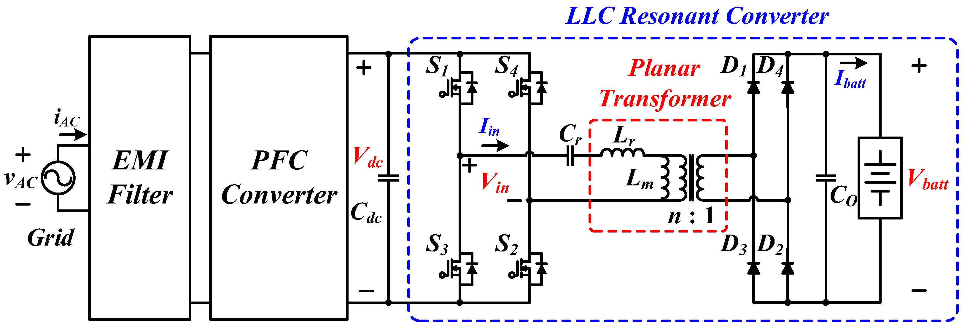
Funding

This work was supported by Korea Institute of Energy Technology Evaluation and Planning(KETEP) grant funded by the Korea government(MOTIE) (20224000000440, Sector coupling energy industry advancement manpower training program).

Data Availability Statement

Not applicable.

Conflicts of Interest

The authors declare no conflict of interest.

References

  1. Iodice, P.; Fornaro, E.; Cardone, M. Hybrid Propulsion in SI Engines for New Generation Motorcycles: A Numerical-Experimental Approach to Assess Power Requirements and Emission Performance. Energies 2022, 15, 6312. [Google Scholar] [CrossRef]
  2. Zhou, K.; Chen, S.M.; Jin, N.Z.; Sun, D.Y. Research on Single-Phase and Three-Phase Compatible Isolated On-board Charger and Control Technology. Energies 2022, 15, 6445. [Google Scholar] [CrossRef]
  3. Yilmaz, M.; Krein, P.T. Review of battery charger topologies, charging power levels, and infrastructure for plug-in electric and hybrid vehicles. IEEE Trans. Power Electron. 2012, 28, 2151–2169. [Google Scholar] [CrossRef]
  4. Khaligh, A.; D’Antonio, M. Global trends in high-power on-board chargers for electric vehicles. IEEE Trans. Veh. Technol. 2019, 68, 3306–3324. [Google Scholar] [CrossRef]
  5. Whitaker, B.; Barkley, A.; Cole, Z.; Passmore, B.; Martin, D.; McNutt, T.R.; Lostetter, A.B.; Lee, J.S.; Shiozaki, K. A High-Density, High-Efficiency, Isolated On-Board Vehicle Battery Charger Utilizing Silicon Carbide Power Devices. IEEE Trans. Power Electron. 2014, 29, 2606–2617. [Google Scholar] [CrossRef]
  6. Li, B.; Li, Q.; Lee, F.C.; Liu, Z.; Yang, Y. A High-Efficiency High-Density Wide-Bandgap Device-Based Bidirectional On-Board Charger. IEEE J. Emerg. Sel. Top. Power Electron. 2018, 6, 1627–1636. [Google Scholar] [CrossRef]
  7. Lim, C.Y.; Jeong, Y.; Moon, G.W. Phase-shifted full-bridge DC-DC converter with high efficiency and high power density using center-tapped clamp circuit for battery charging in electric vehicles. IEEE Trans. Power Electron. 2019, 34, 10945–10959. [Google Scholar] [CrossRef]
  8. Ta, L.A.D.; Dao, N.D.; Lee, D.C. High-efficiency hybrid LLC resonant converter for on-board chargers of plug-in electric vehicles. IEEE Trans. Power Electron. 2020, 35, 8324–8334. [Google Scholar] [CrossRef]
  9. Gadelrab, R.; Yang, Y.; Li, B.; Lee, F.; Li, Q. High-Frequency High-Density Bidirectional EV Charger. In Proceedings of the 2018 IEEE Transportation Electrification Conference and Expo (ITEC), Long Beach, CA, USA, 13–15 June 2018; pp. 687–694. [Google Scholar]
  10. Zhang, Z.; Liu, C.; Wang, M.; Si, Y.; Qin, L. High-efficiency high-power-density CLLC resonant converter with low-stray-capacitance and well-heat-dissipated planar transformer for EV on-board charger. IEEE Trans. Power Electron. 2020, 35, 10831–10851. [Google Scholar] [CrossRef]
  11. Liu, Z.; Li, B.; Lee, F.C.; Li, Q. High-Efficiency High-Density Critical Mode Rectifier/Inverter for WBG-Device-Based On-Board Charger. IEEE Trans. Ind. Electron. 2017, 64, 9114–9123. [Google Scholar] [CrossRef]
  12. Kim, D.H.; Kim, M.J.; Lee, B.K. An Integrated Battery Charger with High Power Density and Efficiency for Electric Vehicles. IEEE Trans. Power Electron. 2017, 32, 4553–4565. [Google Scholar] [CrossRef]
  13. Mukherjee, S.; Ruiz, J.M.; Barbosa, P. A High Power Density Wide Range DC–DC Converter for Universal Electric Vehicle Charging. IEEE Trans. Power Electron. 2023, 38, 1998–2012. [Google Scholar] [CrossRef]
  14. Zhao, S.; Kempitiya, A.; Chou, W.T.; Palija, V.; Bonfiglio, C. Variable DC-Link Voltage LLC Resonant DC/DC Converter With Wide Bandgap Power Devices. IEEE Trans. Ind. Appl. 2022, 58, 2965–2977. [Google Scholar] [CrossRef]
  15. Fan, G.; Wu, X.; Liu, T.; Xu, Y. High-Efficiency High-Density MHz Cellular DC/DC Converter for On-Board Charger. IEEE Trans. Power Electron. 2022, 37, 15666–15677. [Google Scholar] [CrossRef]
  16. Shen, Y.; Zhao, W.; Chen, Z.; Cai, C. Full-Bridge LLC Resonant Converter With Series-Parallel Connected Transformers for Electric Vehicle On-Board Charger. IEEE Access 2018, 6, 13490–13500. [Google Scholar] [CrossRef]
  17. Xu, H.; Yin, Z.; Zhao, Y.; Huang, Y. Accurate Design of High-Efficiency LLC Resonant Converter with Wide Output Voltage. IEEE Access 2017, 5, 26653–26665. [Google Scholar] [CrossRef]
  18. Saket, M.A.; Shafiei, N.; Ordonez, M. LLC converters with planar transformers: Issues and mitigation. IEEE Trans. Power Electron. 2017, 32, 4524–4542. [Google Scholar] [CrossRef]
  19. Djuric, S.; Stojanovic, G.; Damnjanovic, M.; Radovanovic, M.; Laboure, E. Design, Modeling, and Analysis of a Compact Planar Transformer. IEEE Trans. Magn. 2012, 48, 4135–4138. [Google Scholar] [CrossRef]
  20. Ouyang, Z.; Thomsen, O.C.; Andersen, M.A.E. Optimal Design and Tradeoff Analysis of Planar Transformer in High-Power DC–DC Converters. IEEE Trans. Ind. Electron. 2012, 59, 2800–2810. [Google Scholar] [CrossRef]
  21. Li, S.; Min, Q.; Rong, E.; Zhang, R.; Du, X.; Lu, S. A Magnetic Integration Half-Turn Planar Transformer and its Analysis for LLC Resonant DC-DC Converters. IEEE Access 2019, 7, 128408–128418. [Google Scholar] [CrossRef]
  22. Ho, G.K.Y.; Pong, B.M.H. Multilayer Flexible Printed Circuitry Planar Transformer with Integrated Series Capacitance for an LLC Converter. IEEE Trans. Power Electron. 2019, 34, 11139–11152. [Google Scholar] [CrossRef]
  23. Saket, M.A.; Ordonez, M.; Craciun, M.; Botting, C. Improving Planar Transformers for LLC Resonant Converters: Paired Layers Interleaving. IEEE Trans. Power Electron. 2019, 34, 11813–11832. [Google Scholar] [CrossRef]
  24. D’Antonio, M.; Chakraborty, S.; Khaligh, A. Planar Transformer with Asymmetric Integrated Leakage Inductance Using Horizontal Air Gap. IEEE Trans. Power Electron. 2021, 36, 14014–14028. [Google Scholar] [CrossRef]
  25. Li, B.; Li, Q.; Lee, F.C. High-Frequency PCB Winding Transformer with Integrated Inductors for a Bi-Directional Resonant Converter. IEEE Trans. Power Electron. 2019, 34, 6123–6135. [Google Scholar] [CrossRef]
  26. Li, M.; Ouyang, Z.; Andersen, M.A.E. High-Frequency LLC Resonant Converter with Magnetic Shunt Integrated Planar Transformer. IEEE Trans. Power Electron. 2019, 34, 2405–2415. [Google Scholar] [CrossRef]
  27. Mu, M.; Lee, F.C. Design and Optimization of a 380–12 V High-Frequency, High-Current LLC Converter with GaN Devices and Planar Matrix Transformers. IEEE J. Emerg. Sel. Top. Power Electron. 2016, 4, 854–862. [Google Scholar]
  28. Fei, C.; Lee, F.C.; Li, Q. High-Efficiency High-Power-Density LLC Converter With an Integrated Planar Matrix Transformer for High-Output Current Applications. IEEE Trans. Ind. Electron. 2017, 64, 9072–9082. [Google Scholar] [CrossRef]
  29. Liu, Y.C.; Chen, C.; Chen, K.D.; Syu, Y.L.; Lu, D.J.; Kim, K.A.; Chiu, H.J. Design and Implementation of a Planar Transformer with Fractional Turns for High Power Density LLC Resonant Converters. IEEE Trans. Power Electron. 2021, 36, 5191–5203. [Google Scholar] [CrossRef]
  30. Iyer, K.V.; Cai, M.; Murthy-Bellur, D.; Palmer, B.; Mohan, N. A half-turn winding for compact, high-current, high-turns-ratio, low-leakage-inductance transformer. In Proceedings of the IEEE Energy Conversion Congress Expo. (ECCE), Cincinnati, OH, USA, 1–5 October 2017; pp. 3222–3227. [Google Scholar]
  31. Li, H.; Zhang, Z.; Wang, S.; Tang, J.; Ren, X.; Chen, Q. A 300-kHz 6.6-kW SiC Bidirectional LLC Onboard Charger. IEEE Trans. Ind. Electron. 2020, 67, 1435–1445. [Google Scholar] [CrossRef]
  32. Li, H.; Bai, L.; Zhang, Z.; Wang, S.; Tang, J.; Ren, X.; Li, J. A 6.6kW SiC bidirectional on-board charger. In Proceedings of the 2018 IEEE Applied Power Electronics Conference and Exposition (APEC), San Antonio, TX, USA, 4–8 March 2018; pp. 1171–1178. [Google Scholar]
  33. Magnetics, Transformer Design with Magnetics Ferrite Cores. Available online: https://www.mag-inc.com/Design/Design-Guides/Transformer-Design-with-Magnetics-Ferrite-Cores (accessed on 22 August 2023).
Figure 1. Single-phase OBC system with planar transformer.
Energies 16 06757 g001
Figure 2. Initial designed planar transformer.
Energies 16 06757 g002
Figure 3. Conceptual diagram of parasitic capacitance inside the PCB pattern.
Energies 16 06757 g003
Figure 4. LLC resonant converter circuit considering equivalent parasitic capacitance.
Energies 16 06757 g004
Figure 5. LLC resonant converter voltage gain curve change with parasitic capacitance size.
Energies 16 06757 g005
Figure 6. JMAG simulation pattern layout for parasitic capacitance measurement. (a) Maximum pattern overlap. (b) Minimum pattern overlap.
Energies 16 06757 g006
Figure 7. JMAG simulation parasitic measurement results according to PCB pattern arrangement. (a) Maximum pattern overlap. (b) Minimum pattern overlap.
Energies 16 06757 g007
Figure 8. PCB internal pattern layout under various conditions. (a) Maximum pattern overlap. (b) Minimum pattern overlap. (c) Intermediate pattern overlap.
Energies 16 06757 g008
Figure 9. Manufactured PCBs under various conditions. (a) Maximum pattern overlap. (b) Minimum pattern overlap. (c) Intermediate pattern overlap.
Energies 16 06757 g009
Figure 10. Impedance characteristic curve according to frequency of various PCBs. (a) Maximum pattern overlap. (b) Minimum pattern overlap. (c) Intermediate pattern overlap.
Energies 16 06757 g010
Figure 11. Voltage gain curve of actual LLC resonant converter with each parasitic capacitance.
Energies 16 06757 g011
Figure 12. Experimental setup of the LLC resonant converter with planar transformer.
Energies 16 06757 g012
Figure 13. Experimental waveforms and efficiency of the LLC converter with different transformer types. (a) Conventional Litz wire. (b) Case 1 planar transformer. (c) Case 2 planar transformer. (d) Case 3 planar transformer.
Energies 16 06757 g013
Figure 14. Various cores for the planar transformer. (a) PEE core. (b) UI core. (c) H core.
Energies 16 06757 g014
Figure 15. Planar transformers manufactured in various core shape. (a) PEE core. (b) UI core. (c) H core.
Energies 16 06757 g015
Figure 16. Experimental waveforms and efficiency of the LLC converter with different transformer core types. (a) PEE core. (b) UI core. (c) H core.
Energies 16 06757 g016
Figure 17. Planar transformer system with water cooling. (a) Planar transformer. (b) Bottom cooling water passage.
Energies 16 06757 g017
Figure 18. Planar transformer PCB manufactured in various pattern widths.
Energies 16 06757 g018
Figure 19. Thermal image of the planar transformer. (a) 3 oz/2 mm. (b) 3 oz/2.5 mm. (c) 3 oz/3 mm. (d) 3 oz/4 mm.
Energies 16 06757 g019aEnergies 16 06757 g019b
Figure 20. Transformer pattern temperature measurement results over time. (a) 3 oz/2 mm. (b) 3 oz/2.5 mm. (c) 3 oz/3 mm. (d) 3 oz/4 mm.
Energies 16 06757 g020
Figure 21. PEE core design dimensions.
Energies 16 06757 g021
Figure 22. Parameters for planar transformer design.
Energies 16 06757 g022
Figure 23. Transformer area and volume according to the number of turns.
Energies 16 06757 g023
Figure 24. Optimally designed planar transformer. (a) 3D model. (b) Manufactured transformer.
Energies 16 06757 g024
Figure 25. Transformer pattern temperature measurement results over time.
Energies 16 06757 g025
Figure 26. Experimental waveforms and efficiency of the LLC converter according to the battery voltage. (a) Vbatt = 440 V. (b) Vbatt = 600 V. (c) Vbatt = 820 V.
Energies 16 06757 g026
Table 1. Specification of the LLC resonant converter.
ParametersValue
DC link voltage, Vdc500 V
Battery voltage, Vbatt440–820 V
Rated output power, Po3.3 kW
Switching frequency, fsw200–450 kHz
Resonant frequency, fres300 kHz
Table 2. Parameters of the LLC resonant converter.
ParametersValue
Magnetizing inductance, Lm79.3 μH
Leakage inductance, Lr25.8 μH
Resonant capacitor, Cr10.91 nF
Turns ratio, n10:12
Table 3. Parasitic capacitance simulation results according to PCB pattern arrangement.
Pattern ArrangementMaximum CapacitanceMinimum Capacitance
Maximize overlap8.14 pF0.77 pF
Minimize overlap2.70 pF0.68 pF
Table 4. Parasitic capacitance measurement results according to PCB pattern arrangement.
CaseLmfresCeq
Case 178.3 μH0.7 MHz676 pF
Case 274.2 μH1.82 MHz103 pF
Case 374.0 μH1.88 MHz96.7 pF
Table 5. Operation verification experimental condition.
ParametersValue
DC link voltage, Vdc500 V
Battery voltage, Vbatt600 V
Rated output power, Po3.3 kW
Resonant frequency, fres300 kHz
Table 6. Characteristics of planar transformer core shape.
Planar TransformerPEE CoreUI CoreH Core
AdvantageLow heightWide pattern heat dissipation areaLow height
Narrow area requiredImplementing a large number of turnsMinimum volume
DisadvantageNarrow pattern heat dissipation areaWide area requiredDifficult pattern heat dissipation
Implementing a large number of turnsHigh heightImplementing a large number of turns
Table 7. Specifications for each planar transformer core shape.
Planar TransformerPEE CoreUI CoreH Core
Size [W × D × H] [mm]60 × 100 × 2296 × 55 × 4164 × 74 × 14
Area6000 mm25280 mm24992 mm2
Volume132,000 mm3216,480 mm369,888 mm3
Magnetizing inductance78.32 μH78.90 μH77.56 μH
Leakage inductance3.98 μH0.73 μH4.67 μH
Table 8. Current density according to pattern width.
ParametersValue
Current9.8 Arms
Thickness3 oz
Width2 mm2.5 mm3 mm4 mm
Current density46.3 A/mm237 A/mm230.9 A/mm223.1 A/mm2
Table 9. Effective area according to the number of turns.
ParameterValue
Np4 turns5 turns6 turns7 turns8 turns9 turns10 turns
Ac1250.0 mm21000.0 mm2833.3 mm2714.3 mm2625.0 mm2555.6 mm2500.0 mm2
Table 10. Spacing distance conditions for planar transformer.
ParametersValue
Spacing distance between patterns, DP-P0.6 mm
Spacing distance between pattern and core, DP-C3 mm
Spacing distance between PCB and core, DPCB-C1 mm
Table 11. Design results of PEE core parameters according to the number of turns.
ParameterValue
Np45678910
Ac1250.0 mm21000.0 mm2833.3 mm2714.3 mm2625.0 mm2555.6 mm2500.0 mm2
A96.6 mm92.4 mm85.8 mm80.6 mm76.4 mm77.6 mm74.8 mm
B46.6 mm40.6 mm37.3 mm34.7 mm32.6 mm29.6 mm28.2 mm
C32.4 mm30.8 mm28.6 mm26.9 mm25.5 mm25.9 mm25.0 mm
D58.6 mm59.9 mm56.5 mm53.9 mm51.8 mm56.0 mm54.6 mm
E38.6 mm32.6 mm29.3 mm26.7 mm24.6 mm21.6 mm20.2 mm
F8 mm8 mm8 mm8 mm8 mm8 mm8 mm
Area63 cm265 cm259 cm254 cm250 cm256 cm254 cm2
Volume294 cm3264 cm3218 cm3186 cm3162 cm3167 cm3151 cm3
Disclaimer/Publisher’s Note: The statements, opinions and data contained in all publications are solely those of the individual author(s) and contributor(s) and not of MDPI and/or the editor(s). MDPI and/or the editor(s) disclaim responsibility for any injury to people or property resulting from any ideas, methods, instructions or products referred to in the content.

