Article

Shielding Strategies for Electric Field Minimization in Current Transformers: A Finite Element Combined Design of Experiment Approach

1
School of Electrical Engineering and Automation, Xiamen University of Technology, Xiamen 361024, China
2
Xiamen Key Laboratory of Frontier Electric Power Equipment and Intelligent Control, Xiamen 361024, China
3
Xiamen DYH Technology Co., Ltd., Xiamen 361101, China
*
Author to whom correspondence should be addressed.
Energies 2023, 16(21), 7247; https://doi.org/10.3390/en16217247
Submission received: 23 August 2023 / Revised: 26 September 2023 / Accepted: 23 October 2023 / Published: 25 October 2023
(This article belongs to the Section F: Electrical Engineering)

Abstract

:
The internal electric field distribution is a key factor to characterize the partial discharge and voltage resistance of current transformers (CTs), and the conical current transformer has a special structure with complex electric field distribution. Therefore, it is more necessary to study, analyze and optimize the electric field distribution of CTs in the design process. In this paper, a new type of current transformer is taken as the research object. A simulation model is established by using finite element software, and the electric field distribution under the test of power-frequency withstand voltage is investigated. Then, a scheme is proposed, and the response surface is used to optimize the scheme. Experimental verification is conducted to validate the results. In this study, the finite element combined design of experiment approach can serve as a rapid and efficient approach for identifying an optimal solution to minimize the electric field strength within a current transformer.

1. Introduction

Partial discharge is a common issue with current transformers (CTs), which can lead to changes in the electric field distribution and molecular structure of the insulation. This deterioration in insulation performance can even result in breakdown [1]. To prevent such phenomena, it is important to analyze the electric field distribution and maximum electric field in the transformer, which can provide a theoretical basis for optimizing the structure of the transformer [2,3]. Recent years have seen an increase in the number of electric field analyses and studies conducted on S F 6 CTs with high voltage levels [4,5]. However, there has been a relative lack of studies on the electric field analysis of poured CTs. Conventional mathematical expressions is typically used to analyze very simple geometries [6,7]. This methodology necessitates the involvement of engineers with significant theoretical knowledge and practical experience in engineering, often resulting in challenges when designing and analyzing multiple operating points.
Recently, in order to determine the optimal conductive rod diameter for a poured CT, Dong utilized finite element simulation software to calculate the electro-thermal coupling field distribution characteristics of the CT under different currents, temperatures, and diameters of conductive rod. However, the study only simulated four groups of conductive rod diameters to derive the optimal diameter, without conducting a more comprehensive parameter search [8]. Jia conducted a simulation of the electric field distribution for a 400 kV DC CT using finite element analysis. The study also involved calculating the electric field distribution and dense areas at different voltages. The results obtained from the simulation were compared with those under S F 6 gas [9]. In order to address the issue of uneven E-field strength distribution in current transformers, Wu’s study proposed a method to enhance the weakness part of the insulation baffle inside the transformer [10]. This method relied on the electric field analysis of a pillar type current transformer using ANSOFT Maxwell software to obtain the distribution inside the transformer. Wu then identified the area of electric field concentration near the winding for local analysis and compared the magnitude of the improved local field strength to reach an optimized conclusion. However, the study did not provide the best method for achieving the desired outcome. Literature [11] determined the various characteristics of the load distribution and electric field distribution in the withstand voltage test through the finite element simulation of the ±1100 kV epoxy resin transformer and verified the results through experiments. In order to address the issue of the 500 kV substation failure in Peru, Ricardo conducted a finite element simulation of the transformer located within the substation. This simulation calculated the maximum electric field, concentrated electric field area, and inhomogeneous electric field distribution. Additionally, a brief analysis of the causes of the faults was conducted [12]. In order to optimize the insulation performance of current transformers and solve their flash or partial discharge problems, optimization schemes for the internal structure of the CT have been proposed in several studies, and the electric field distribution calculated by finite element method has been used to compare the results of several different optimization schemes with the tests of a realistic model. The optimized products performed well in tests [13,14,15,16]. Literature [17] conducted an electrostatic field simulation for various factors affecting transformer grounding current and obtained the grounding current under different factors. This paper presents the design and simulation of a conical current transformer with a voltage rating of 40.5 kV.
According to the client’s order, a special conical structure is needed to fit the installation. Therefore, a new conical CT was designed with the primary and secondary windings encapsulated into a single unit using epoxy resin. The secondary side core is typically rolled with strip silicon steel sheet. Compared to oil-immersed current transformers, this design offers higher mechanical strength, lighter weight, better insulation performance, and improved reliability performance [18,19,20]. Additionally, the internal medium of cast-resin type current transformers is epoxy resin, which is more environmentally friendly than S F 6 type current transformers. The global warming potential (GWP) of S F 6 is 23,900 times higher than that of C O 2 , and the leakage of SF6 into the atmosphere will exacerbate the ongoing global warming phenomenon [21,22,23].
In this paper, a 40.5 kV conical current transformer is modeled in a 3D structure. The rest of this paper is organized as follows. In Section 2, the transient simulation model is established by using finite element software. In Section 3, the electric field distribution under the power-frequency withstand voltage test (85 kV, 1 min) is studied to locate the point with the maximum value. Then, a scheme is proposed, and the maximum values before and after optimization are compared. In Section 4, the significance of three geometrical factors on the effect of the scheme is examined. Then, an optimized scheme is proposed by using response surface. In Section 5, a partial discharge detection platform is utilized for local discharge measurement. The results of the study can provide a reference for the design of new current transformer for factory production.

2. Establishment of Transient Field Finite Element Model

The Finite Element Method (FEM) is a versatile numerical analysis technique that can be applied to solve a wide range of engineering problems. It provides an approximation of the solution to boundary problems encountered in engineering [24]. FEM is used to dissect the field domain of the research object and divide it into numerous small and simple units, and cater to different accuracy requirements by reducing the physical prototype. In this study, all simulations are conducted through COMSOL Multiphysics software.
Considering the unsymmetrical structure of the current transformer, the traditional two-dimensional FEM cannot calculate the electric field distribution under unsymmetrical boundary condition. Therefore, this paper uses a refined 3D model to calculate the electric field characteristics of the current transformer. As illustrated in Figure 1, the body of the current transformer consists of two copper primary terminals ①, a copper conductive rod ② on the primary side, an iron bracket ③, and an iron secondary coil core ④. The primary side elements are soldered with metallic copper to ensure good electrical conductivity. In order to improve the electric field distribution, the internal conductor part of the CT is casted in epoxy resin after winding the semiconductor shield. Before casting, it is filled with S F 6 gas and pressurized to expel air. Additionally, the body and the cast-resin body are chamfered and polished to further improve the electric field distribution. The diameter of the conductive rod varies according to the rated current on the primary side, and the conductive rod with a diameter of 30 mm at 1250 A is the object of this paper. Table 1 shows the material and physical properties of each original component of the current transformer.
To reduce computational load during the simulation test, the size of the computational field under the AC/DC electrostatic field problem is limited. This is achieved by selecting an appropriate boundary to simulate infinity. In this paper, an outer box, the dimensions of which are five times of those of CT, is set to represent the computational field. The transformer is positioned at the center of the box. The outer surfaces of box is selected as zero electric potential surfaces. The simulation is conducted through one alternating current (AC) cycle by using COMSOL Multiphysics finite element software, and the criteria for the simulation termination are in accordance with the national standardization [25].

Physical Model

In the electrostatic field problem, the electric field can be solved for each point using Maxwell’s system of equations. Equation (1) is the system of Maxwell’s equations in a differential form.
· D = ρ · B = 0 × E = B t × H = J D t .
In Equation (1), J is the conduction current density. For the dispersion equation · D = ρ of the electric field in the above equation, under each homogeneous dielectric condition ( ε = 0 ), Equation (2) can be obtained by bringing in D = ε E = ε φ ,
2 φ = ρ ε .
This equation is the Poisson equation for the electrostatic field. If there is no charge in the computational domain, when ρ = 0 , Equation (2) can be written as
ε 2 φ = 0 .
The equation is in the Laplace form for the electrostatic field. When solving the problem using the finite element method in the electrostatic field, in addition to the equations in the differential form described above, it is necessary to set boundary conditions to determine the uniqueness of the solution.
In this simulation, the secondary side of the current transformer is grounded, and the induced electric field strength ( B / t ) can be neglected. Therefore, the calculation can be regarded as under the electric quasi-static field (EQS). Moreover, under AC conditions, there is no space charge: ρ = 0 ; thus, the control equation of the electric field can be expressed as
d i v D = 0 E = φ .
In order to simulate the power-frequency test, the primary side terminals and the conductive rod of the CT were used, 85 kV 50 Hz AC was applied, while secondary coil and bracket were grounded.

3. Simulation Results and Analysis

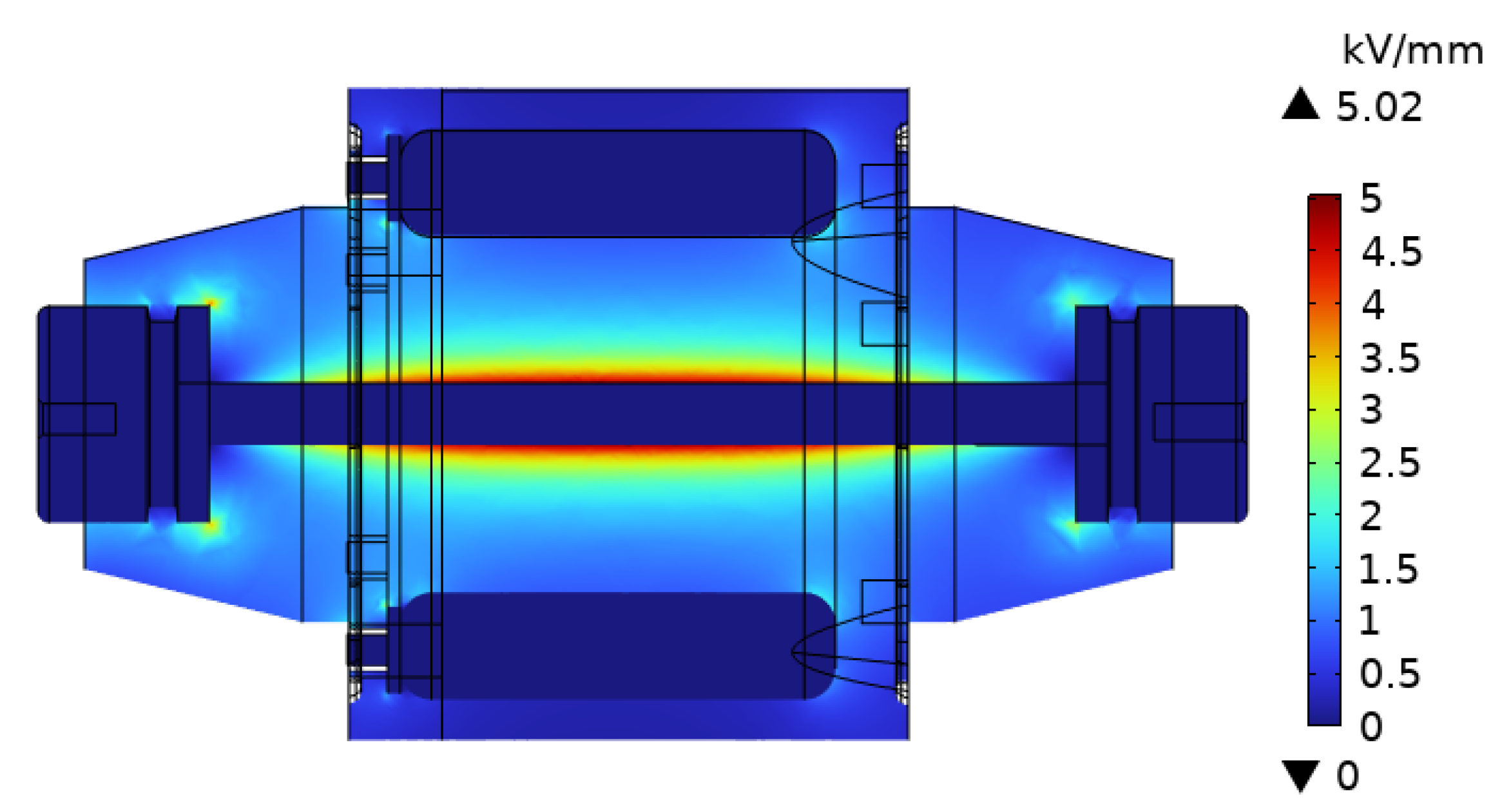
3.1. Electric-Field Distribution of Current Transformer

In order to observe the internal electric field distribution of the transformer, we set the longitudinal direction of the transformer to be the X-axis and the radial direction to be the Z-axis. The X-Z plane is selected as the observation plane. Figure 2 presents the cross-sectional view of the X-Z plane of the simulation. The electric field in the cross-sectional view is found to be mainly concentrated near the conductive rod, the surfaces of inserts, and the end of the terminals.
The transformer’s withstand voltage and partial discharge value can be impacted by the maximum electric field strength and its location. The maximum electric field strength and its location in the computational domain is shown in Figure 3. It shows that the maximum electric field strength in the transformer is 11.5561 kV/mm near the air gap. We define that point as P m a x , the coordinates of which are x( 95.000 ), y( 0.652 ), z( 71.042 ). A probe is positioned at P m a x to analyze the variations of electric field in two cyclicalities. The results in Figure 4 show that the electric field varies uniformly and reaches its maximum at 0.005 s, which corresponds to the peak moment of applied voltage.
In this paper, the bracket is installed with metal inserts and is directly exposed without being wrapped in epoxy resin. It is a weak part in the transformer for the electric field. Therefore, it is necessary to analyze the electric field in the vicinity of the insert. Figure 5 depicts the variation of electric field intensity along the x-axis near the insert, where the path is represented by the blue line within the diagram. The electric field strength gently varies from 0 to 4.6 mm along the X axis, while near the peak, it varies considerably, resulting in uneven distribution. The fluctuations are also considerable near 6.46 mm. The uneven distribution of the electric field can cause the transformer in the factory test to malfunction, leading to a discharge phenomenon. To balance the distribution, the transformer’s structure will be redesigned and the electric field distribution before and after optimization will be compared.

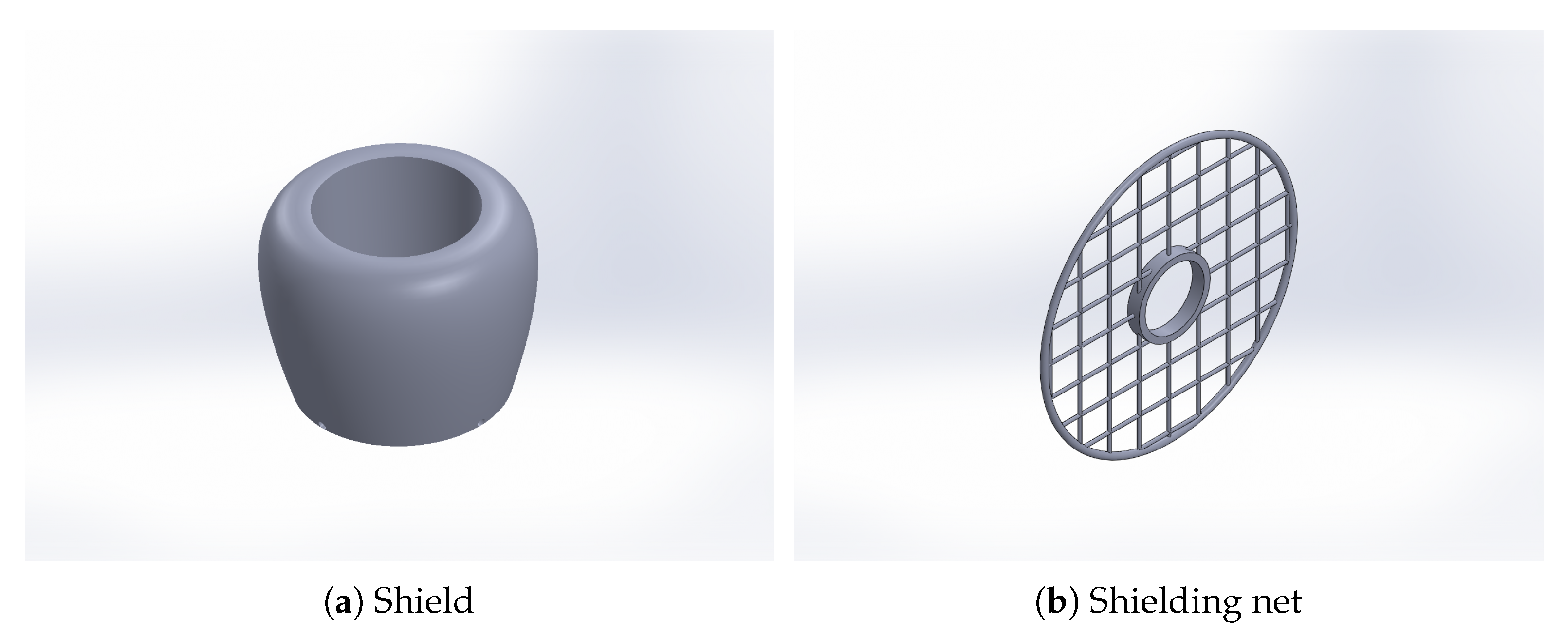
3.2. Optimization Scheme

The most common method of balancing the internal electric field distribution of a transformer is using a metal shield or a shielding net shown in Figure 6. A shield is typically employed at the end of capacitive insulation structures in vertical or inverted transformers. The shields are often designed in a columnar shape to balance the electric field exposed in the air and to reduce local discharge signals. A shielding net is often used in cast-resin type CTs, generally installed behind the transformer terminals, to allow the maximum electric field strength appearing on the shielding net to improve the transformer’s ability to withstand voltage. This paper proposes an optimization scheme for the transformer, which involves adding a shielding net with a radius of 42 mm and a wire diameter of 4 mm, positioned 70 mm from the primary terminal. The optimized internal electric field, circled in red, is primarily concentrated on the shielding net shown in Figure 7.
The maximum field strength in the optimized computational domain is on the inner surface of the shielding net with a value of 15.9492 kV/mm. Figure 8 displays the location of the maximum electric field in the computational domain, indicating a shift from the insert to the inner surface of the net, from the exposed part to the internal. Since the breakdown electric field strength of the epoxy resin is greater than 30 kV/mm, the internal electric field strength of the transformer remains within a safe value. Figure 9 shows the variation of electric field at the original maximum point P m a x during the simulation after improvement. The electric field strength at that point significantly declines throughout the calculation time, from the value of 11.5561 kV/mm to 5.0419 kV/mm. The improvement results are prominent.
Figure 10 displays a comparison of the electric field on the surface of the insert. The line graph illustrates a smoother distribution of values near the peak, where the maximum value of the electric field distribution on the axial distance is reduced from 6.46 kV/mm to 6.34 kV/mm.
The location of the maximum electric field of the current transformer shifts from the external insert to the internal net surface after the shielding net is added. The electric field strength at P m a x decreases from 11.5561 kV/mm to 5.0419 kV/mm, and the distribution near the insert over the axial distance is smoother. The comparison results show that the addition of a shielding mesh to the transformer enacts a certain improvement on the electric field.

4. Design of Experiment and Response Surface

Design of experiments (DOE) is a statistical theory and methodology used to observe how changing input factors affects the output response. By analyzing the effect of each input factor on the output response, DOE helps to optimize the input factors for the desired output response. This process involves the use of mathematical statistics to obtain information [26]. For the experimental design to the above scheme, three factors of the shielding net, radius, wire diameter, and the location of installation, were selected as the variable input factors, and the maximum electric field a point P m a x was selected as the response result. In this study, DOE analysis was conducted through Minitab software.

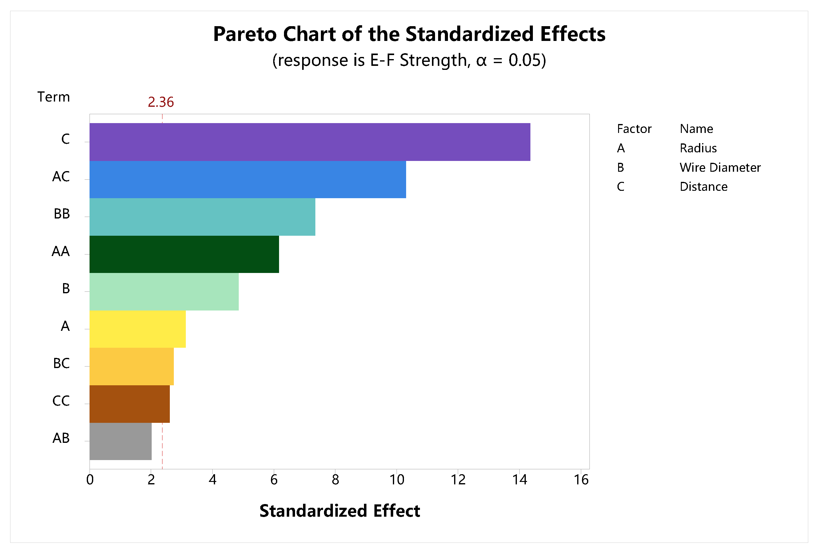
4.1. Selection of Factors

To design the response surface, it is necessary to determine the input factor and its range of values. For the electrical design, it is important that the shielding net is at least 15 mm away from the surface of the casting body to ensure proper insulation. Therefore, the maximum radius of the shielding net can be up to 42 mm. However, if the minimum radius is less than 35 mm, the simulation results, as shown in Figure 11 circled in red, indicate that the maximum electric field appears at the end of the terminal rather than on the shielding net. As a result, the minimum radius of the shielding net must be 35 mm.
The wire diameter level of the outer ring of the shielding net is limited to 1–4 mm due to production constraints. Additionally, the installation position is restricted to be after the primary terminal and before the secondary coil, while also ensuring a distance of at least 15 mm from the surface of the casting body. As a result, the installation distance ranges from 55 to 85 mm to the surface of the primary terminal. Table 2 displays the selected impact factors and their corresponding value ranges.

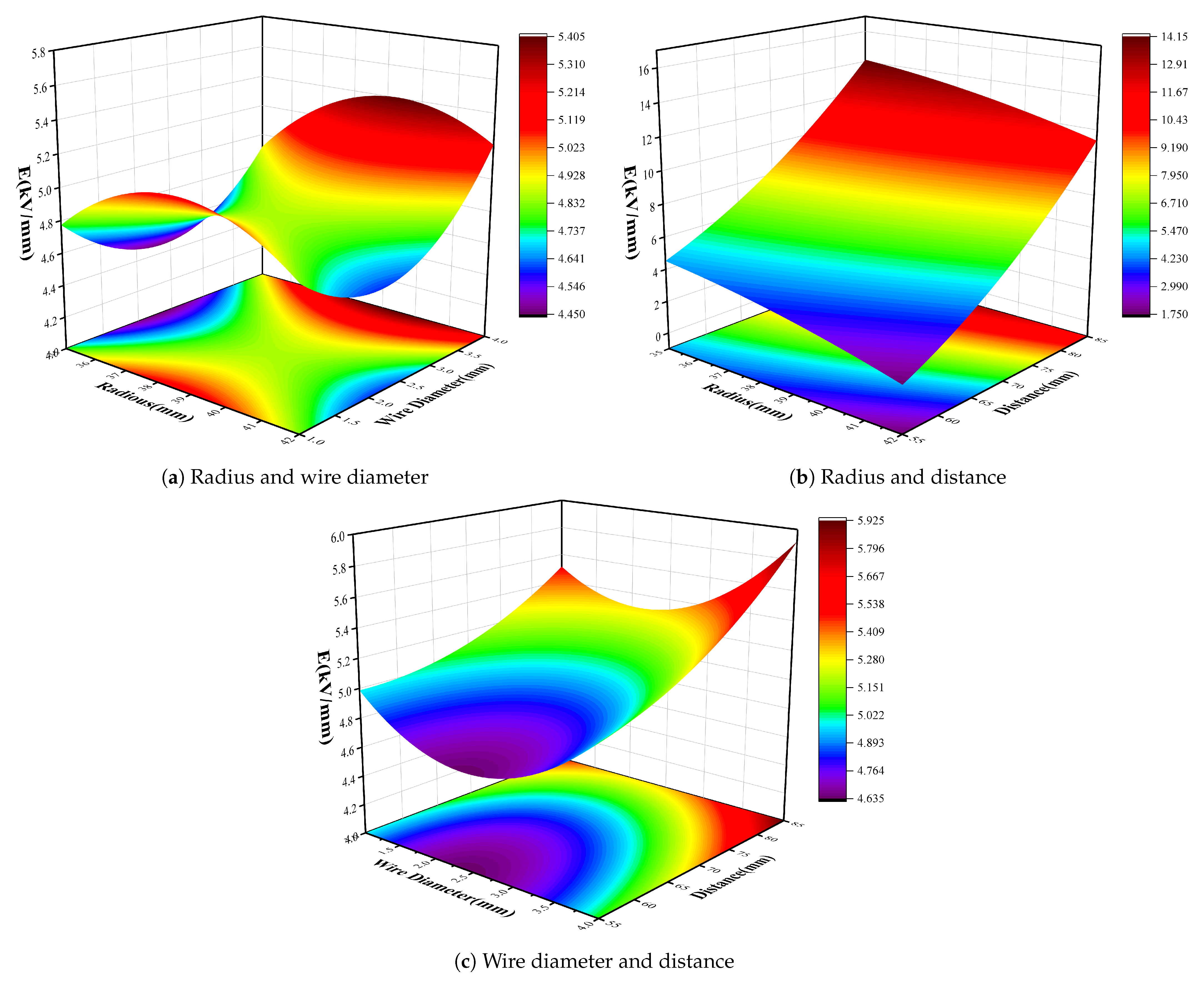
4.2. Establishment of Response Surface

In this paper, a Central Composite Experimental Design (CCED) including three-time center point experiments was conducted to analyze the effects of the factors above. The generated randomized trial sequence table was as depicted in Table 3. In Table 3, StdOrder is the Standard Order of CCED which must run randomly. PtType is the Point Type of CCED, where 1 means the center point of surface, 0 means the center point of body, and 1 means the vertex. All values of factors are shown in a digital format, where 1 means a low level, 0 means a medium level, and 1 means a high level. A total of 17 simulation trials were conducted in accordance with the Run Order. The simulation results were assigned to their experimental groups, respectively, for factor analysis. To achieve a more accurate fit, a second-order model should be considered, which incorporates the interaction between the three factors and their squared term effects. Figure 12 shows the Pareto diagram of the influencing factors obtained by using Minitab software. From the diagram, the factors and interaction effects on the response are d i s t a n c e > d i s t a n c e a n d r a d i u s i n t e r a c t i o n > w i r e d i a m e t e r 2 > r a d i u s 2 > w i r e d i a m e t e r > r a d i u s > w i r e d i a m e t e r a n d d i s t a n c e i n t e r a c t i o n > d i s t a n c e 2 . The interaction effect between radius and wire diameter is insignificant and is removed in the subsequent analysis process.
After removing the insignificant interaction effect, the model’s response surfaces were established, and are shown in Figure 13. The response surfaces between the parameters reveal that in the simple model, the interaction effect between some parameters is evident. For instance, in Figure 13a, the surface of radius and wire diameter interaction is ‘saddle-shaped’, indicating that the interaction effect is not prominent. In Figure 13b, the contour line of radius and distance interaction is ‘stepped’, indicating that the interaction effect has the most significant impact on the electric field. In Figure 13c, the contour line of the interaction of line diameter and distance is circular, suggesting that the interaction effect is significant.
Table 4 shows that the minimum predicted electric field strength, which is the result of response surface, is 4.053 kV/mm when the radius is 42 mm, the wire diameter is 2.2727 mm, and the installation distance is 55 mm. To verify this optimal response, the simulation model parameters were modified, and the maximum electric field strength obtained from the point P m a x was found to be 4.16982 kV/mm, which is only 2.89% different from the DOE analysis. This is illustrated in Figure 14.

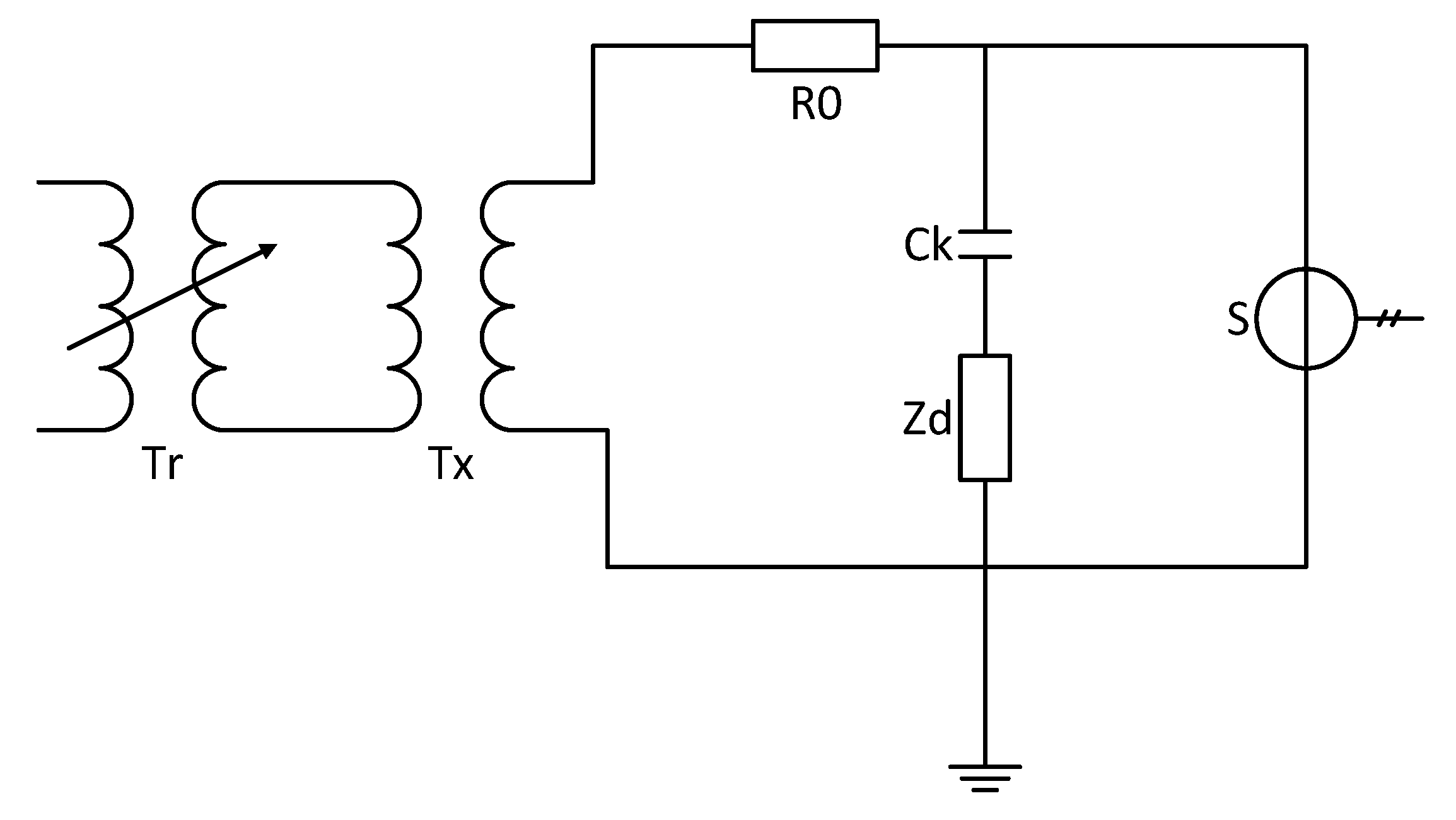
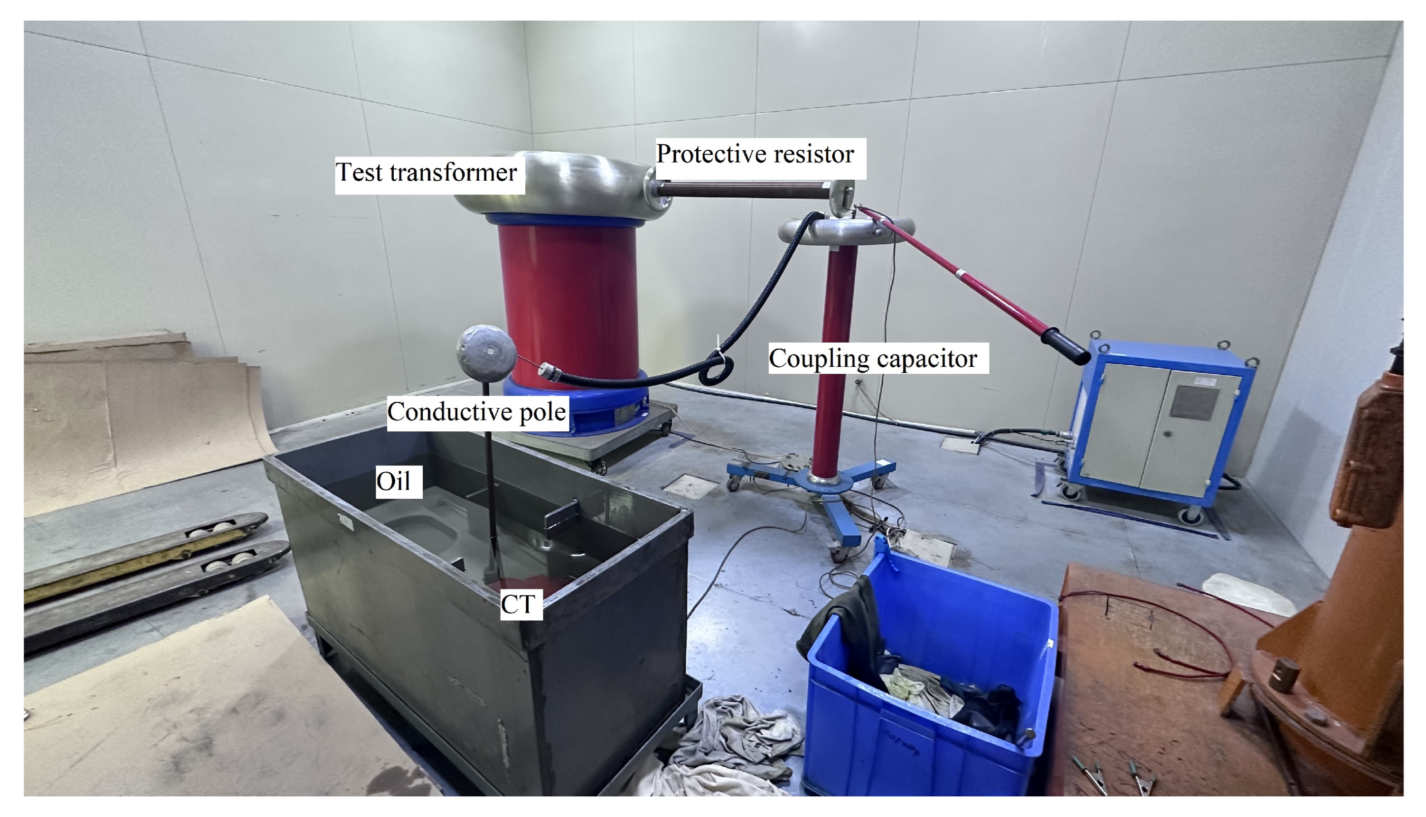
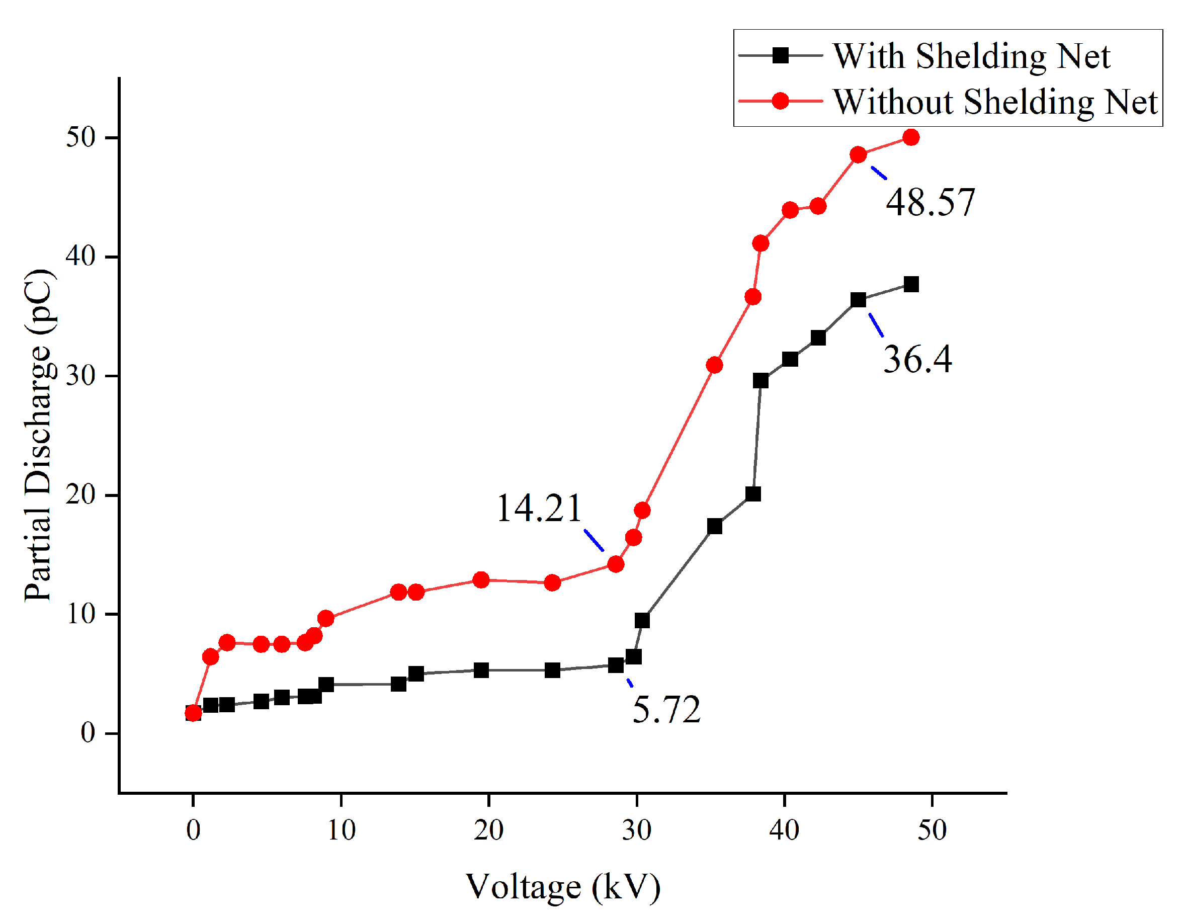
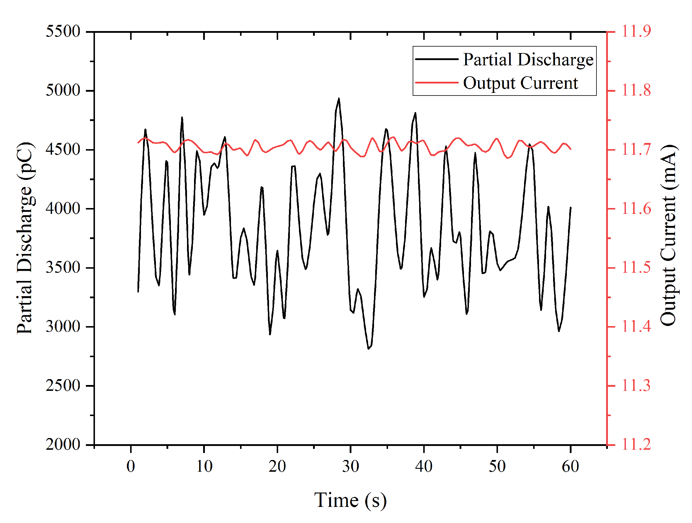
5. Partial Discharge Test

Figure 15 presents a schematic diagram of the primary side circuit, established according to the (PRC) National Standard of CT partial discharge test [25]. The circuit comprises the test transformer T r , the power-frequency test transformer T x , the protective resistor R 0 , the partial discharge measuring instrument C k , the detecting impedance Z d , and the CT S that requires testing. The system generates a pulse current partial discharge signal, which is obtained through the coupling capacitor and directly sent to the local discharge measuring instrument. A photo of the test station is shown in Figure 16.
The partial discharge meter measured a background signal of 1.70 pC after the conectining was completed without applying voltage. The partial discharge signal of the current transformer before and after improvement is shown in Figure 17. Before improvement, the meter measured 14.21 pC in the low-voltage state, 48.57 pC in the high-voltage state, and the comparison result was 5.72 pC at a low voltage and 36.4 pC at a high voltage, which was 60% lower after improvement. The optimization effect is obvious. The CT withstand voltage test at 62 kV showed an obvious discharge phenomenon without the addition of a shielding net. However, after optimization, it could withstand up to 85 kV in 1 min without any discharge. Figure 18 shows the power-frequency withstand voltage experiment data. When there is a discharge, the current signal significantly surges to zero.

6. Conclusions

In this paper, the electric field distribution of a new type of CT during voltage withstand test is investigated. The simulation model of the CT is established in this paper, and an improvement scheme is proposed. The DOE is conducted on the effects of radius, wire diameter and shielding position on the E-field distribution to obtain the optimal solution. Finally, the factory voltage withstand test is conducted for verification. The main conclusions of the study are as follows:
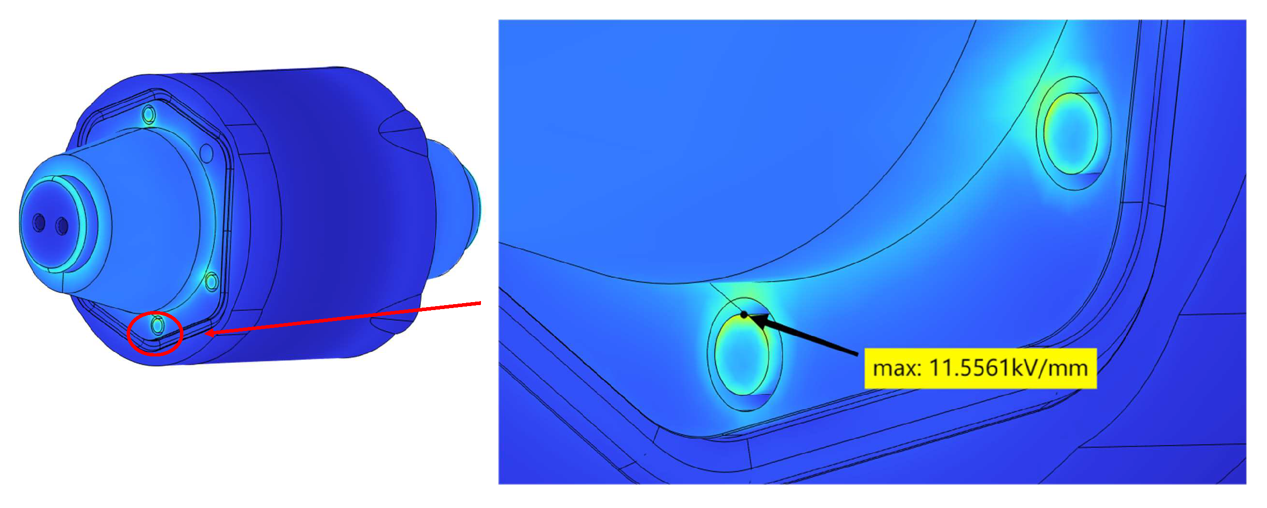
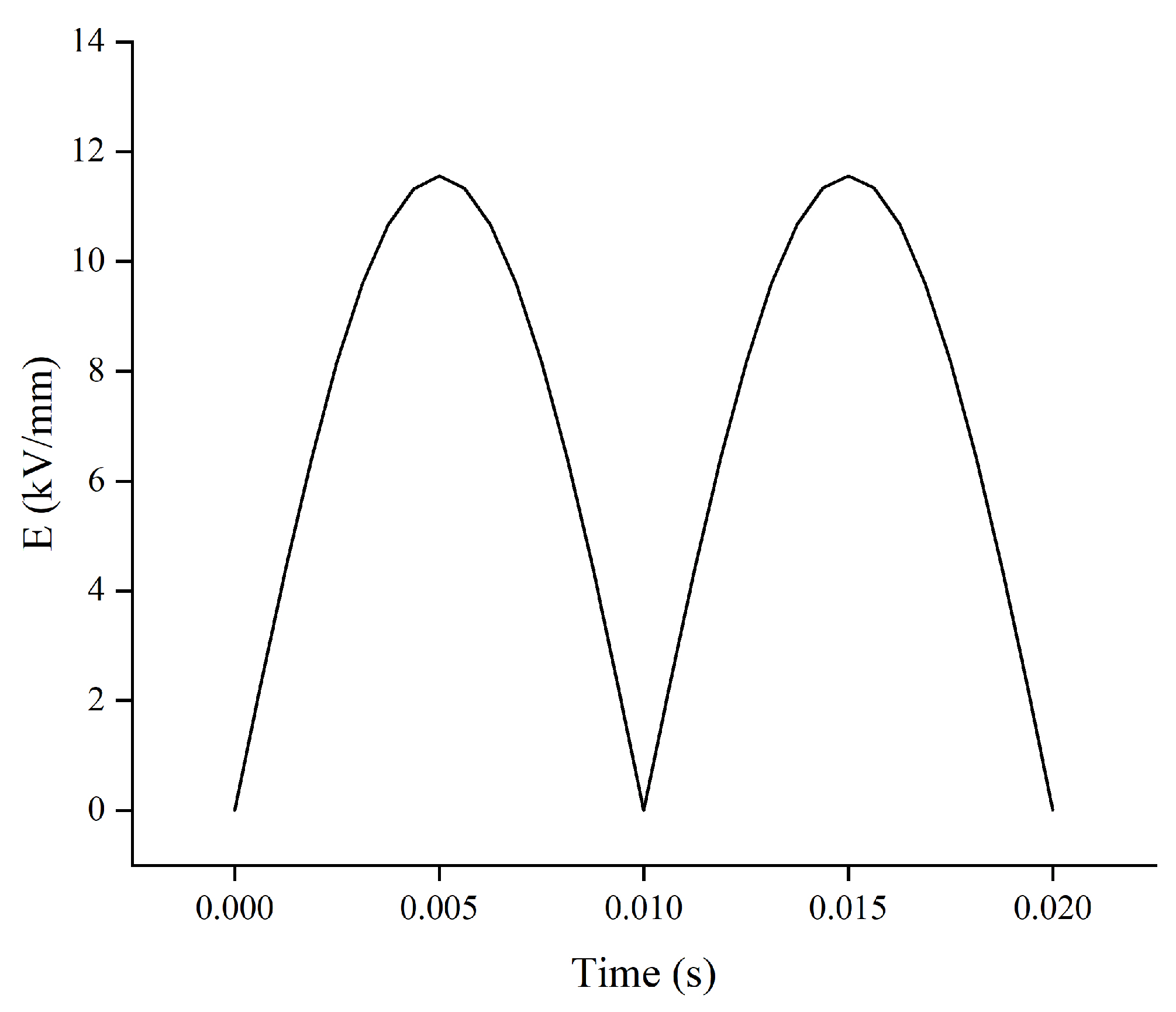
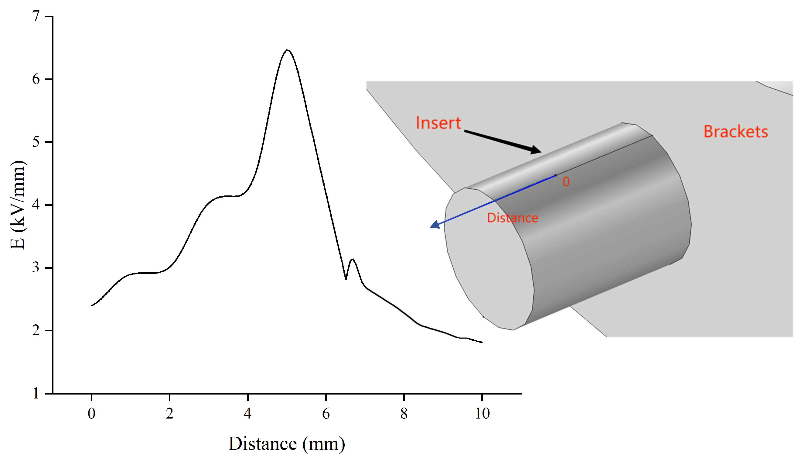
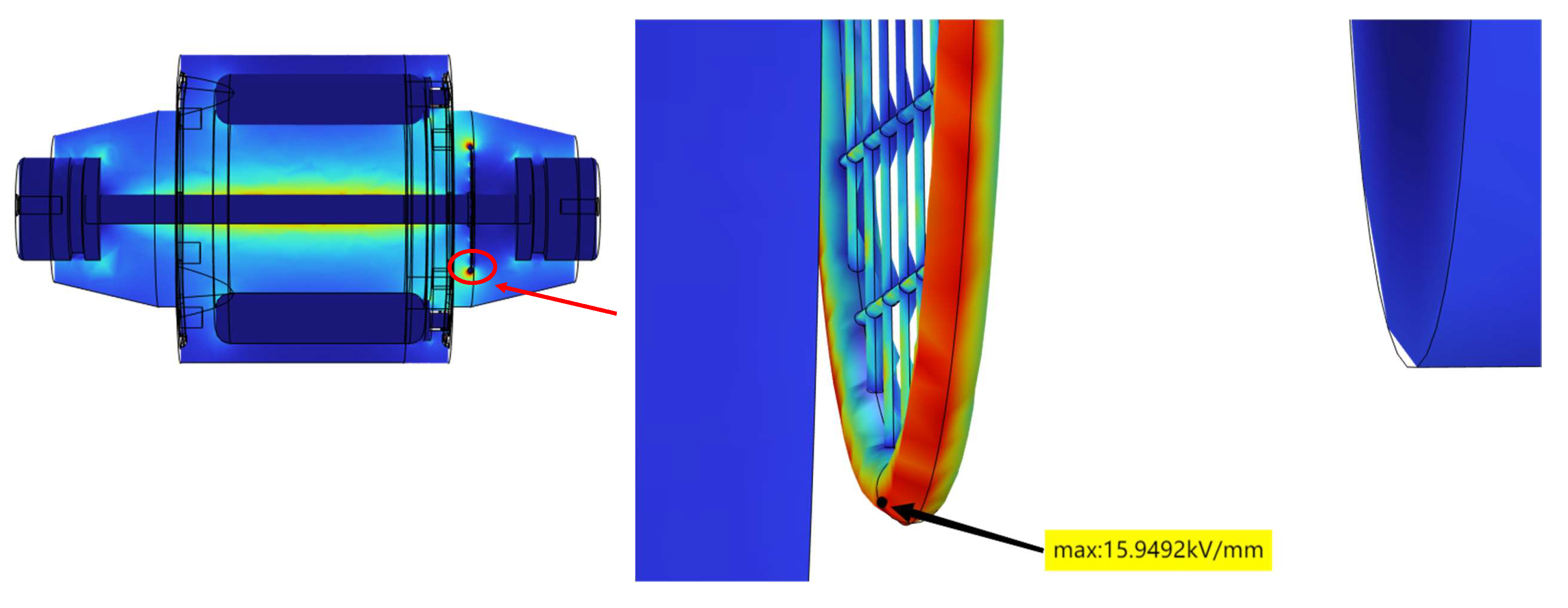
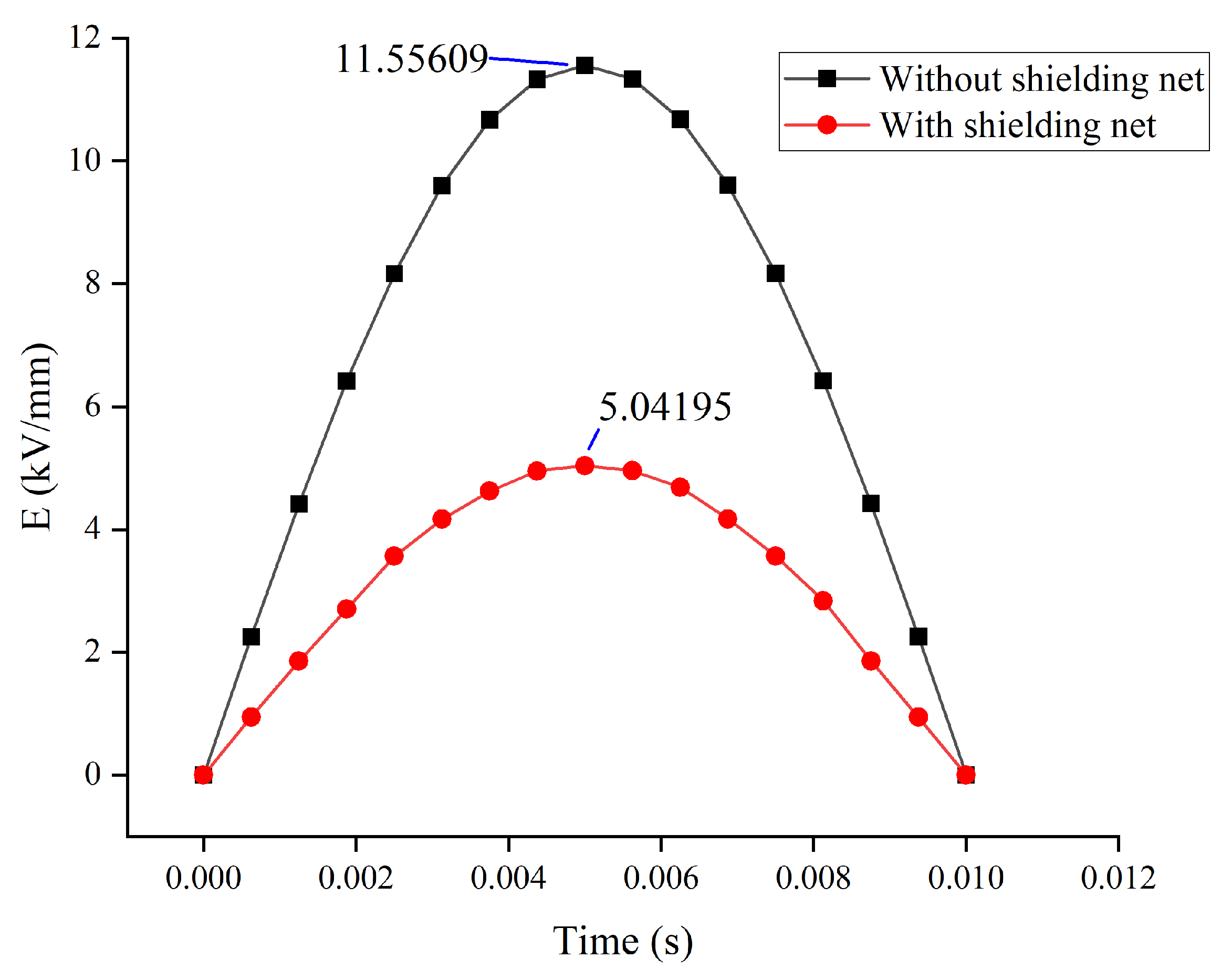
  • The weak area of the electric field distribution in the CT is found near the metal insert of the bracket. When the input voltage is at its maximum, the electric field strength is 11.5561 kV/mm. At P m a x , the electric field on the surface of the insert distributes unevenly along the axial direction.
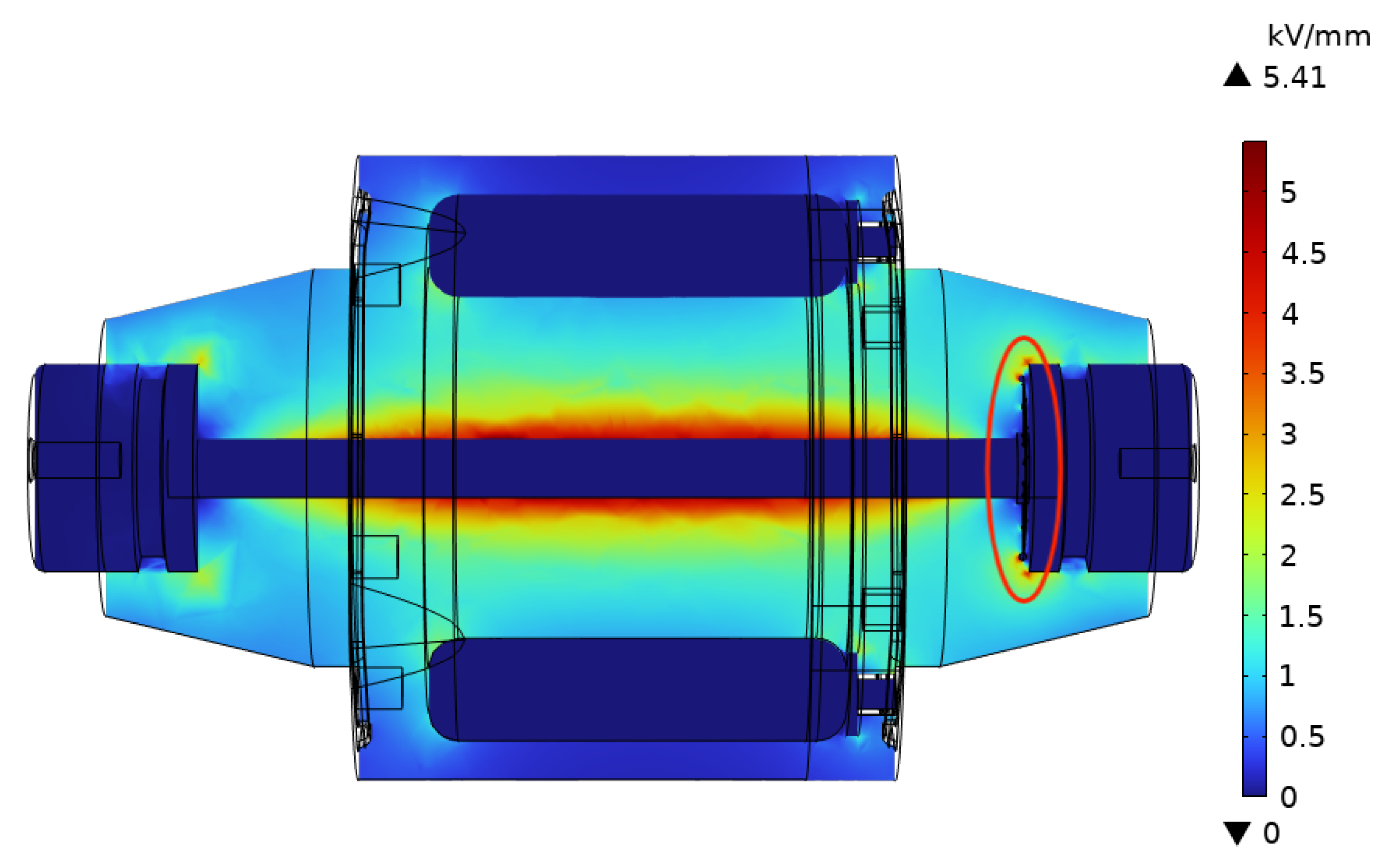
  • After optimization, the maximum electric field in the current transformer is located on the shielding net, with a value of 15.9492 kV/mm. The electric field strength at P m a x is reduced to 5.0419 kV/mm, which is a decrease of 56.37%.
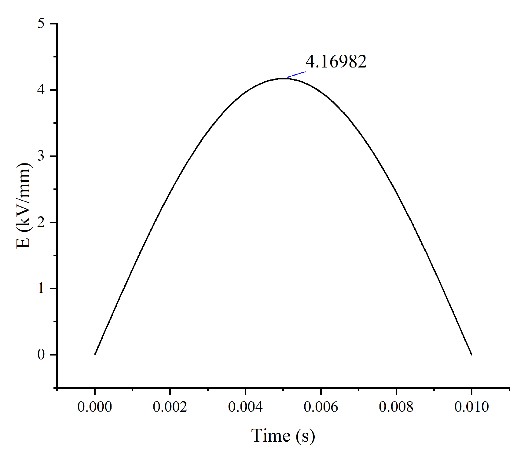
  • The response surfaces predict the minimum electric field strength is 4.053 kV/mm when the radius is 42 mm, the wire diameter is 2.2727 mm, and the position is 55 mm. The simulation result is 4.16982 kV/mm.
  • The optimization effect is obvious when the improved CT is subjected to partial discharge test. Without a shielding net, the CT withstand voltage test at 62 kV appears obviously discharging. After optimization, it can withstand up to 85 kV in 1 min without discharging.
  • In this paper, a finite element combined design of experiment approach is used for optimization. Future research could try to use a more systematic algorithm, such as neural network combined with genetic algorithm, to select more factors that may affect the electric field for optimization and compare it with the method in this paper.

Author Contributions

Conceptualization, J.Z.; Methodology, J.Z. and X.Y.; Simulation, X.Y.; Validation, X.Y. and Q.G.; Writing—Original draft preparation, X.Y.; Writing—Review and editing, J.Z. and Q.G.; Funding Acquisition, J.Z. All authors have read and agreed to the published version of the manuscript.

Funding

This research was funded by Natural Science Foundation of Fujian Province, grant number 2020J01282, and by the Xiamen Key Laboratory of Frontier Electric Power Equipment and Intelligent Control, Xiamen 361024, China.

Data Availability Statement

Data available on request due to restrictions, e.g., privacy or ethical. The data presented in this study are available on request from the corresponding author. The data are not publicly available due to manufacturer’s trade secret.

Conflicts of Interest

The authors declare no conflict of interest.

References

  1. Feng, Y. Study on the Relationship between Surface Discharge and Decomposition Gas of Basin Insulators for SF6 Current Transformers. Ph.D. Thesis, Shandong University, Jinan, China, 2021. [Google Scholar]
  2. Xiuke, Y.; Yang, S.; Cunzhan, Y.; Dexin, X. Electric Field Analysis and Optimal Design of Main Insulation for Oil-Immersed Inverted Current Transformers. Trans. China Electrotech. Soc. 2014, 29, 37–43. [Google Scholar]
  3. Thango, B.A.; Bokoro, P.N. Defining and Specifying Design Considerations for Distribution Transformers in Large-Scale Solar Photovoltaic Plants. Energies 2022, 15, 2773. [Google Scholar] [CrossRef]
  4. Dameng, H.; Nianping, Y.; Zhongyi, W.; Junxin, T.; Jiancang, M. Electric Field Analysis and Experimental Study of Defective Basin Insulators Within SF6- Gas-Insulated Current Transformers of 500 kV. Electr. Power 2014, 47, 27–32. [Google Scholar]
  5. Guo, L.; Yu, Z.; Bo, L.; Tao, D.; Yongyi, Z. Optimal design of insulation of current transformers cast by epoxy resin at high altitude. High Volt. Electr. Appl. 2010, 46, 57–60. [Google Scholar]
  6. Ana, D.; Bojan, T. Transformer electric field calculation using BEM and FEM. Procedia Eng. 2017, 202, 312–318. [Google Scholar]
  7. Dalibor, F.G.; Božidar, F.G.; Miroslav, P. Electric field at sharp edge as a criterion for dimensioning condenser-type insulation systems. Electr. Power Syst. Res. 2017, 152, 485–492. [Google Scholar]
  8. Dong, B.; Gu, Y.; Gao, C.; Zhang, Z.; Wen, T.; Li, K. Three-Dimensional Electro-Thermal Analysis of a New Type Current Transformer Design for Power Distribution Networks. Energies 2021, 14, 1792. [Google Scholar]
  9. Jia, J.; Xu, J.; Wen, Z. Electric Field Distribution in SF 6 Gas of Converter Transformer Bushing under Complex Voltages. In Proceedings of the IEEE International Conference on High Voltage Engineering and Application, Beijing, China, 6–10 September 2020. [Google Scholar]
  10. Xiaodong, W.; Wenwen, G.; Shudi, Z.; Gaolin, W.; Qian, W.; Xiaoping, L.; Huixian, H. Finite element analysis of electric field and structural optimization design of 10 kV cast strut type current transformer. J. Southwest Univ. 2019, 41, 134–140. [Google Scholar]
  11. Qingyu, W.; Peng, L.; Huidong, T.; Gengsheng, X.; Zongren, P.; Xi, Y. Research on the dynamic characteristics of electric field distribution of the 1100 kV Ultra high voltage converter transformer valve-side bushing using weakly ionised gas conductance model. High Volt. 2022, 7, 288–301. [Google Scholar]
  12. Ricardo, M.A.V.; Jennifer, V.M.L. Current transformer failure caused by electric field associated to circuit breaker and pollution in 500kV substations. Eng. Fail. Anal. 2018, 92, 163–181. [Google Scholar]
  13. Lesniewska, E.E.; Olak, J. Improvement of the Insulation System of Unconventional Combined Instrument Transformer Using 3-D Electric-Field Analysis. IEEE Trans. Power Deliv. 2018, 33, 2582–2589. [Google Scholar] [CrossRef]
  14. Wei, W.; Hanbo, Z.; Jinhua, H.; Xiaogang, L.; Yuquan, L.A. 500kV current transformer flashover failure cause analysis. Transformer 2016, 53, 64–67. [Google Scholar]
  15. Benshuai, Z.; Fenfang, W.; Bo, W.; Haocun, C.; Jiatao, L. ANSYS finite element software simulation and analysis of 145 kV SF6 current transformer. Telecom Power Technol. 2020, 37, 87–89. [Google Scholar]
  16. Anguraja, R.; Dixit, P. Electric Field Distribution of 800 kV OIP Transformer Bushing. Lect. Notes Electr. Eng. 2022, 783, 1784–1792. [Google Scholar]
  17. Huang, K.; Cheng, J.; Wang, S.; Bao, L.; La, Y.; Zhang, Y. Field-Circuit Coupled Simulation of Core Grounding Current of a VSC Transformer. In Proceedings of the 2022 IEEE International Conference on High Voltage Engineering and Applications (ICHVE), Chongqing, China, 25–29 September 2022. [Google Scholar]
  18. Yang, S. Analysis and Optimization Design of Main Insulation Electric Field of Oil-Immersed Inverted Current Transformer. Ph.D. Thesis, Shenyang University of Technology, Shenyang, China, 2012. [Google Scholar]
  19. Xuan, L.; Shipu, W.; Ping, W. Design and performance verification of ultra-high voltage small-capacity capacitive voltage transformer with series damping elements. High Volt. Technol. 2018, 44, 1844–1852. [Google Scholar]
  20. Jaafar, M.J.; Muhamad, N.A.; Jamil, M.K.M.; Rosle, N. Electric Field and Potential Changes Studies on Cast-Resin Dry-Type Power Transformer Having Misalignment. In Proceedings of the 13th IEEE International Conference on the Properties and Applications of Dielectric Materials, Virtual, 12–14 July 2021. [Google Scholar]
  21. Mansour, D.E.A.; Kojima, H.; Hayakawa, N.; Hanai, M.; Okubo, H. Physical mechanisms of partial discharges at nitrogen filled delamination in epoxy cast resin power apparatus. IEEE Trans. Dielectr. Electr. Insul. 2013, 20, 454–461. [Google Scholar] [CrossRef]
  22. Yongsheng, W.; Mingbin, P.; Wenyong, J.; Tongyu, L.; Yanan, W. Feasibility study on substitution of SF6 insulated current transformer with environment-friendly natural gas. Energy Rep. 2023, 9, 1784–1792. [Google Scholar]
  23. Kieffel, Y.; Irwin, T.; Ponchon, P.; Owens, J. Green gas to replace SF6 in electrical grids. IEEE Power Energy Mag. 2016, 14, 32–39. [Google Scholar] [CrossRef]
  24. Hu, F. Study of Stress and Electric Field Simulation of Internal Defects in GIS Tub Insulators and Their Detection Methods. Ph.D. Thesis, North China Electric Power University, Beijing, China, 2017. [Google Scholar]
  25. GB/T 50150–2016; Electric Equipment Installation Engineering-Standard for Hand-Over Test of Electric Equipment. Standardization Administration of the People’s Republic of China: Beijing, China, 2016.
  26. Montgomery, D.C. Design and Analysis of Experiments; John Wiley & Sons: Hoboken, NJ, USA, 2020. [Google Scholar]
Figure 1. Three-dimensional model of the current transformer. 1: Primary terminals. 2: Conductive pols. 3: Brackets. 4: Secondary coil core. 5: Pouring body. 6: Metal insert. The transformer is immersed in Oil (not shown in the figure).
Energies 16 07247 g001
Figure 2. Transformer X-Z plane electric field distribution.
Energies 16 07247 g002
Figure 3. Location of maximum field strength without shielding net.
Energies 16 07247 g003
Figure 4. Electric field strength at P m a x . Time is corresponding to one period of applied AC voltage.
Energies 16 07247 g004
Figure 5. Electric field distribution near the insert along X axis.
Energies 16 07247 g005
Figure 6. Shield and Shielding net.
Energies 16 07247 g006
Figure 7. Optimized X-Z plane electric field distribution.
Energies 16 07247 g007
Figure 8. Location of maximum field strength with shielding net.
Energies 16 07247 g008
Figure 9. Variation of E-field at the point P m a x . Time is corresponding to half a period of applied AC voltage.
Energies 16 07247 g009
Figure 10. Electric field distribution near the optimized insert.
Energies 16 07247 g010
Figure 11. Electric field distribution with a radius of less than 35 mm.
Energies 16 07247 g011
Figure 12. Pareto chart of impact factors.
Energies 16 07247 g012
Figure 13. Response surface.
Energies 16 07247 g013
Figure 14. Simulation results at P m a x with predicted factors.
Energies 16 07247 g014
Figure 15. Circuit diagram.
Energies 16 07247 g015
Figure 16. Test station.
Energies 16 07247 g016
Figure 17. Partial discharge comparison.
Energies 16 07247 g017
Figure 18. Voltage withstand test under 85 kV AC voltage.
Energies 16 07247 g018
Table 1. Material properties.
ComponentsMaterialsElectrical Conductivity
(S/m)
Relative Dielectric Constant
Primary terminalsCopper 5.998 × 10 7 1
Conductive polesCopper 5.998 × 10 7 1
BracketsIron 10.295 × 10 6 1
Secondary Coil CoreIron 10.295 × 10 6 1
Pouring bodyEpoxy resin 2 × 10 14 3.5
Oil 0.3 × 10 12 2.2
The properties are referred from [8].
Table 2. Range of factor values.
FactorLow LevelHigh Level
Radius (mm)3542
Wire diameter (mm)14
Distance (mm)5585
Table 3. Experimental sequence.
Std Order 1Run OrderPt Type 2Radius
(mm)
Wire Diameter
(mm)
Distance
(mm)
E-F Strength
(kV/mm)
101 1 1004.56949
721 1 115.27290
93 1 1 004.45780
341 1 1 1 4.80860
6511 1 15.67650
8611116.09160
47111 1 4.60530
2811 1 1 4.29080
129 1 0105.40000
151000004.91300
171100004.90000
1112 1 0 1 05.04776
1313 1 00 1 4.63900
5141 1 1 14.87040
1151 1 1 1 4.97230
161600004.90410
1417 1 0015.31000
1 Standard Order. 2 Point Type.
Table 4. Predicted result.
Radius
(mm)
Wire Diameter
(mm)
Distance
(mm)
Prediction of Electric Field Size
(kV/mm)
422.2727554.053
Disclaimer/Publisher’s Note: The statements, opinions and data contained in all publications are solely those of the individual author(s) and contributor(s) and not of MDPI and/or the editor(s). MDPI and/or the editor(s) disclaim responsibility for any injury to people or property resulting from any ideas, methods, instructions or products referred to in the content.

