Abstract
This article presents a design method for the active power decoupling (APD) circuit of a PFC converter for high power density on-board chargers (OBCs) utilized in electric vehicles (EVs). The utilization of electrolytic capacitors to mitigate power ripple at the input is a common practice in PFC converters. However, these electrolytic capacitors are associated with issues such as limited lifetime and low current ratings, resulting in a significant portion of the OBC’s volume being occupied by them. To address these challenges and achieve power density, the relationship between the power of the APD circuit and DC-link voltage is derived, and a design method for the APD circuit for high power density is proposed. The feasibility of this design approach is validated through the PFC converter prototype designed for 6.6 kW OBC. Consequently, a substantial volume reduction of 19.7% is realized when compared to the utilization of the electrolytic capacitor approach, and a reduction of 36.2% is achieved in comparison to the conventional APD design method. This reduction in volume proves advantageous for fulfilling the requisites of high power density OBCs.
1. Introduction
Currently, nations around the world are strongly supporting research activities to reduce dependence on fossil fuels and reduce dangerous air pollutants due to abnormal climate change, i.e., global warming [1]. The biggest of these changes is the replacement of internal combustion engine vehicles with electric vehicles (EVs), which increase energy conversion efficiency and reduce greenhouse gas emissions. Therefore, as the demand for EVs increases, a significant amount of related research is being conducted. The EV charging system field aims to secure faster charging times and longer driving mileages for user convenience. The key research topics in the charging field are high power density and high efficiency [2,3,4,5]. Achieving high power density is important because it allows the driving mileage to be increased by reducing the size of the power conversion system (PCS) and mounting more batteries. On-board chargers (OBCs) are vital components of EVs that are responsible for efficient charging. A typical single-phase OBC consists of a power factor correction (PFC) converter that increases the power factor and a DC–DC converter that performs electrical isolation and controls battery charging [6,7,8]. In single-phase OBC, the PFC converter controls the AC side input current so that it is in phase with the input voltage; therefore, in addition to the constant average power supplied to the DC load, a low-frequency power ripple of 120 Hz occurs, which degrades performance.
In general, high-capacity electrolytic capacitors, with a passive power decoupling (PPD) method commonly used in OBCs, are employed to reduce power ripple [9,10,11]. Electrolytic capacitors have a higher single-element capacitance than film capacitors, but their relatively low current rating requires the use of a large number of capacitors in parallel. This can lead to problems with reduced power density and also causes reliability issues because the lifetime is shorter than that of film capacitors. Therefore, a great deal of research has been done on active power decoupling (APD) methods that use additional active circuits to eliminate large electrolytic capacitors [9,10,11]. Research on conventional APD circuits has been applied to renewable energy, such as solar power, where power density is not important. This is because the addition of switches and passive elements cause the volume and cost of the APD circuit to increase compared to the existing PPD method. Additionally, efficiency is reduced because power consumption increases due to additional switches. However, as the reliability of EVs has recently become important, research on the applicability of APD has become necessary. For EVs, achieving high power density is important to increase driving mileage and fuel efficiency. When applying the APD circuit to OBCs, the volume may increase due to additional circuits and the use of a large-volume film capacitor, so analysis is required.
The APD circuit typically comprises power semiconductor devices, inductors for storing power ripple, and film capacitors. Prior research has explored various APD circuit topologies, including buck-boost [12], capacitor split [13,14], and H-bridge types [15,16,17,18], along with control techniques for estimating passive element sizes. However, previous studies have tended to reduce the DC-link capacitance to absorb all power ripple, leading to an increase in system volume due to bulky film capacitors. The DC-link voltage in single-phase OBCs exhibits a ripple tolerance that aligns with the regulation characteristics of the employed DC–DC converter. Therefore, there is no need for the APD circuit to absorb all of the ripple power, and if this is used, the capacity of the film capacitor used in the APD circuit can be reduced, resulting in a volume reduction effect.
Therefore, in this paper, an optimal design approach is introduced that is aimed at enhancing the power density of OBCs incorporating the APD circuit. The relationship between the absorbed power of the APD circuit and the tolerance for DC-link voltage ripple is analyzed, and a design technique that can reduce the capacitance of the film capacitor is proposed. In addition, the proposed design method’s capacity reduction and volume reduction effects according to the ripple power absorption rate are applied to the 6.6 kW OBC structure for electric vehicles to verify its feasibility. The remainder of this paper is organized as follows: Section 2 proposes the system configuration, specifications, and optimal design method for APD circuits. Section 3 verifies the validity via simulation and experimental results, and Section 4 concludes the paper.
2. Design of APD Circuit for High Power Density
2.1. Conventional APD Circuit Design
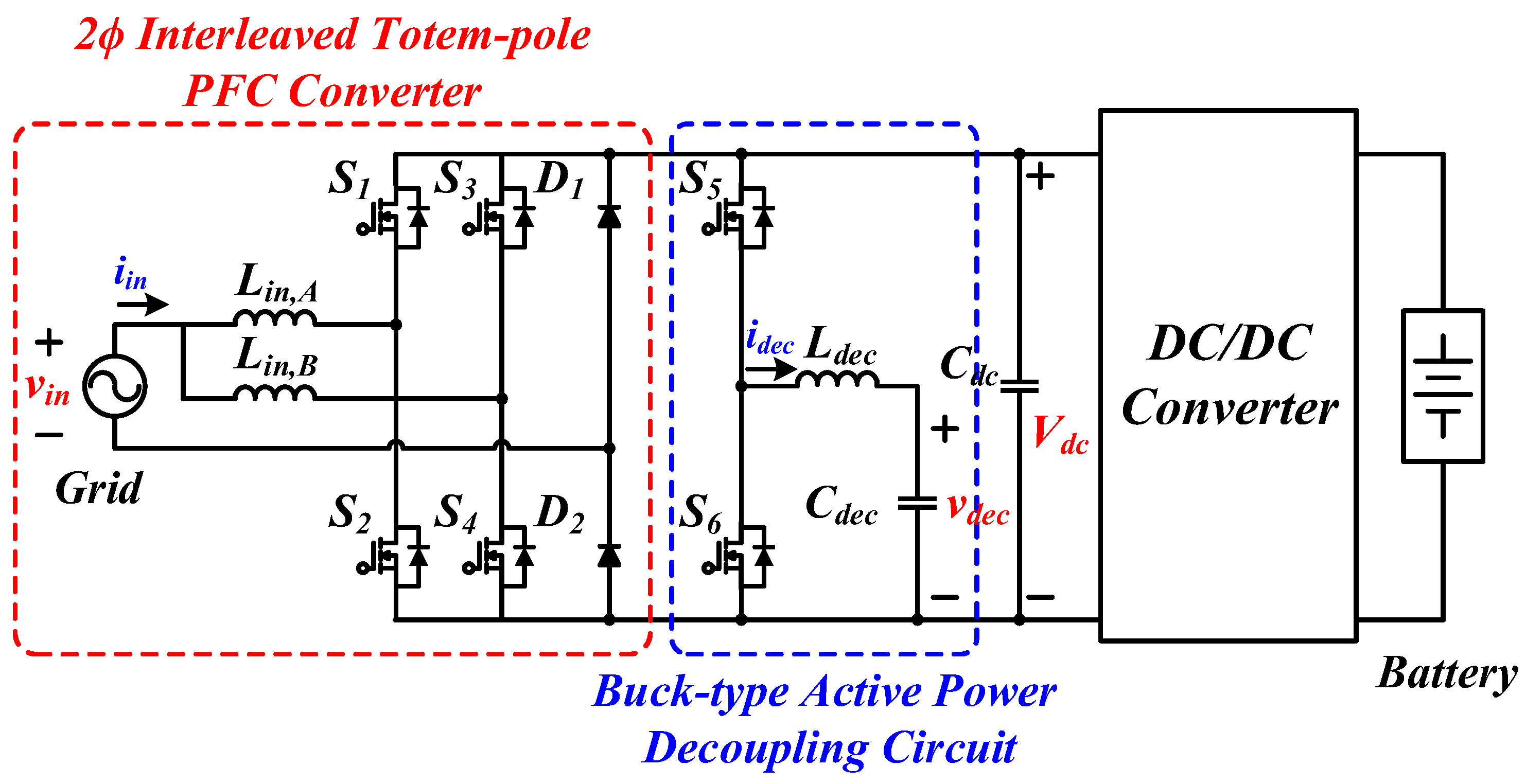
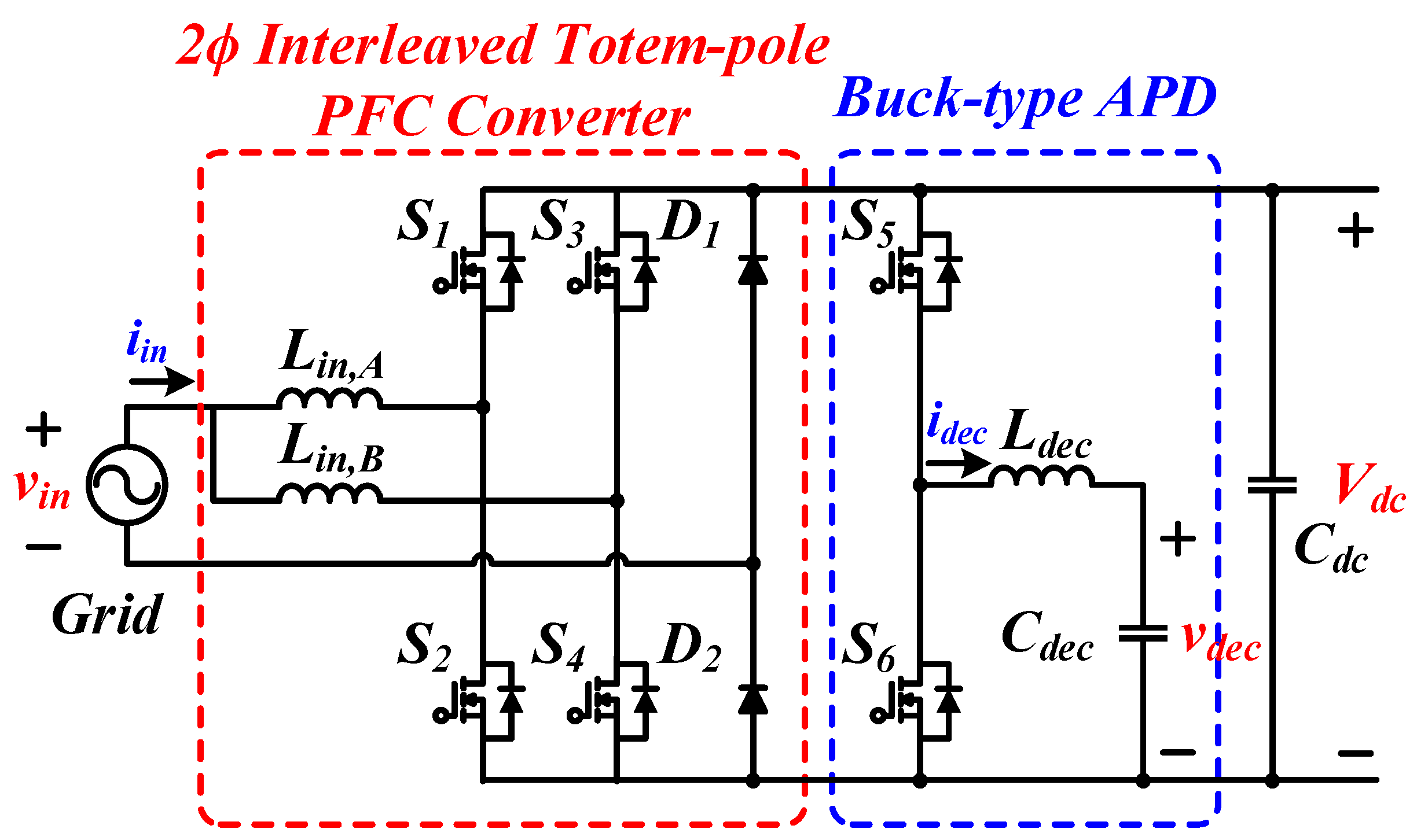
Figure 1 illustrates the PFC converter in a single-phase 6.6 kW OBC with an APD circuit applied. The PFC converter uses a two-phase interleaved totem-pole configuration, while the APD circuit utilizes a buck-type design that can operate independently from the PFC converter. Table 1 presents the design specifications of the PFC converter, which is responsible for input power factor correction and DC-link voltage control. Meanwhile, the APD circuit is in charge of power decoupling control.
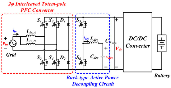
Figure 1.
PFC converter in a 6.6 kW single-phase OBC with APD circuit.

Table 1.
Specifications of a 6.6kW single-phase PFC converter with APD circuit.
The power decoupling control allows the power ripple prip to be absorbed by the power pdec out of the input power Pin,, which the APD circuit stores in the decoupling capacitor Cdec, as Figure 2 illustrates. The expression for pdec is as follows:
then pdec can be reconstructed from the voltage and current relationship of the decoupling capacitor as follows:
by combining (1) and (2), voltage and current in the APD circuit are expressed as follows:
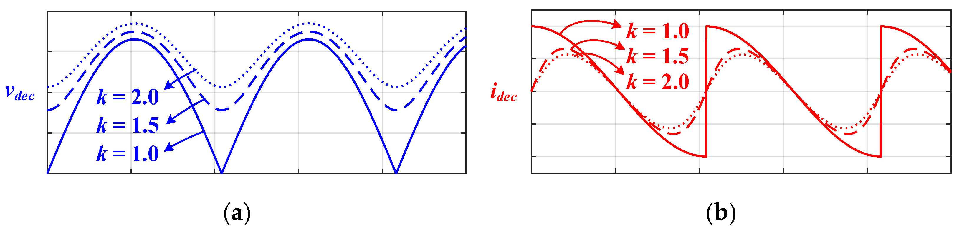
here, k is a parameter that defines the ratio of the energy capacity of Cdec to the amount of energy absorbed by the APD circuit. It has a value of 1 or more and can be expressed as follows:
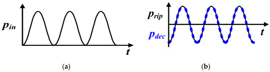
Figure 2.
Control power for the APD circuit. (a) Input power. (b) Decoupling power and power ripple.
Figure 3 illustrates the change of vdec and idec according to the k. Through (3), when k = 1, vdec fluctuates from 0 to the maximum voltage, and through (4), idec fluctuates rapidly with the current slope. In this case, minimizing the size of Cdec is possible, but controlling the point at which vdec reaches 0 becomes challenging. Therefore, designing k to have a value greater than 1 offers advantages in terms of controlling the voltage and current in a sine wave form [19,20].
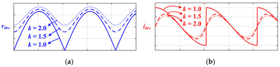
Figure 3.
Voltage and current waveform of the APD circuit according to k. (a) Voltage. (b) Current.
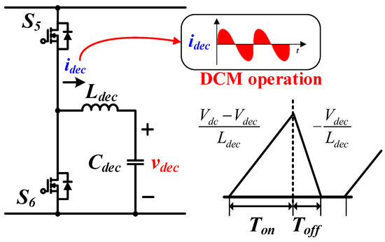
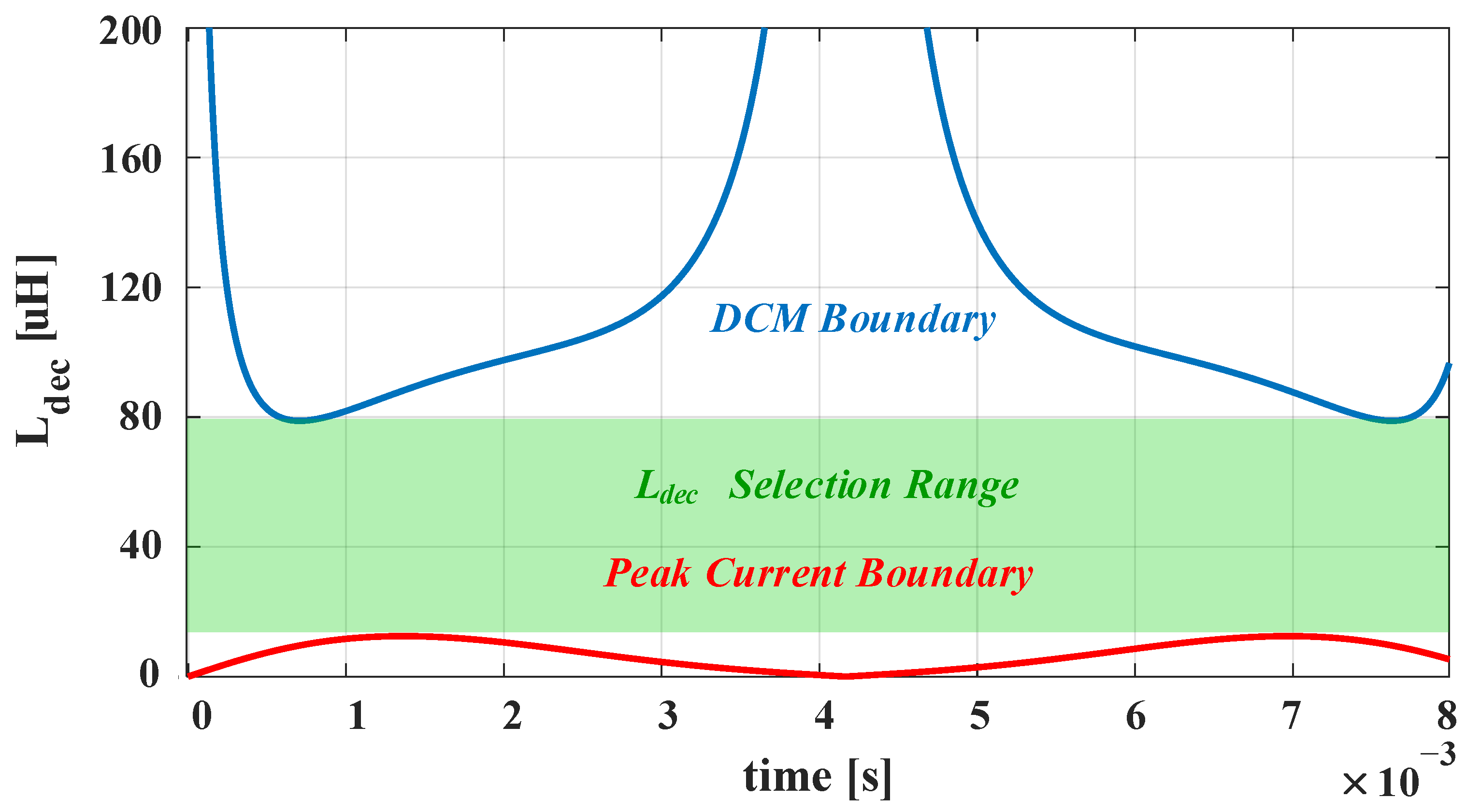
Therefore, the initial design of the APD circuit begins with the decoupling inductor Ldec. Ldec is responsible for delivering ripple power to Cdec and is designed to operate in discontinuous current mode (DCM) to minimize its volume. Figure 4 illustrates the current waveform of Ldec when the APD circuit operates in DCM. Ldec is subject to two design criteria. First, since the DCM operation must be maintained throughout all periods, the following equation must be satisfied.
 though (6), the upper limit size condition of Ldec is as follows:
Figure 4.
Ldec current waveform of APD circuit during DCM operation.
Figure 4.
Ldec current waveform of APD circuit during DCM operation.
Secondly, the peak value of the DCM current must not exceed the maximum current rating of the switch used. Therefore, the lower limit size condition of Ldec is as follows:
The design range of Ldec is determined through (7) and (8) as follows:
Therefore, Figure 5 illustrates the range of Ldec that satisfies the 6.6 kW design condition in this study. To meet the switching frequency requirement and enhance power density. Ldec is chosen to 40 μH and it is designed by stacking two High-Flux CH330060 cores.
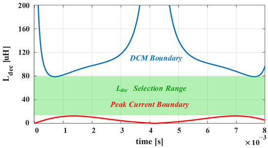
Figure 5.
Ldec design range of the APD circuit.
Next, the design of Cdec can be expressed as follows using (3):
Regarding the size of Cdec, similar to Ldec, a value of k is selected as 1.1 to minimize the capacity. The size of the maximum Vdec values is selected as 650 V, and Table 2 presents the parameters and device information of the APD circuit designed based on this.
Table 2.
APD circuit design result with conventional design method.
Since the purpose of this study is to design a PFC converter for high power density OBC, Table 3 presents the results of comparing the volume of the conventional PPD circuit using only electrolytic capacitors and the designed APD circuit.
Table 3.
Volume analysis of conventional design method.
As a result, the total capacitance used is reduced by approximately 70%. Nevertheless, the addition of elements, along with the transition from electrolytic capacitors to film capacitors, led to an increase in volume, resulting in a 25% overall volume increase. Therefore, it is necessary to propose the APD circuit design method to achieve high power density.
2.2. Proposed APD Circuit Design
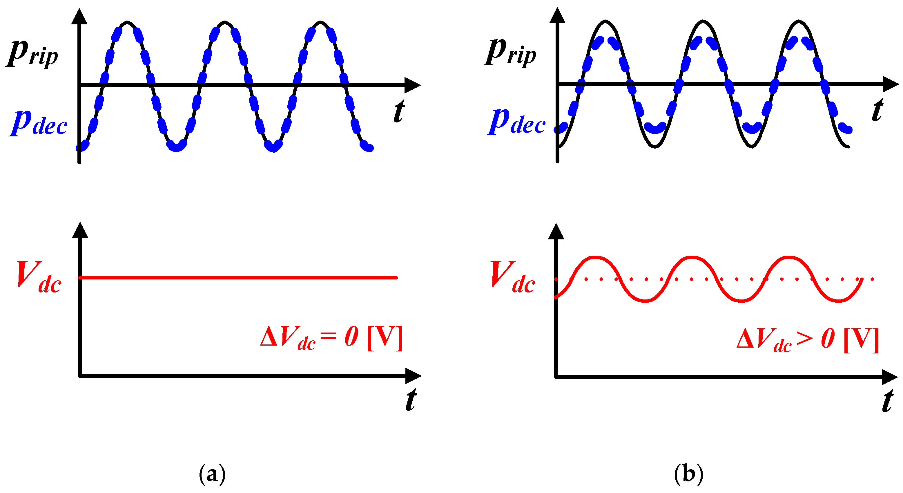
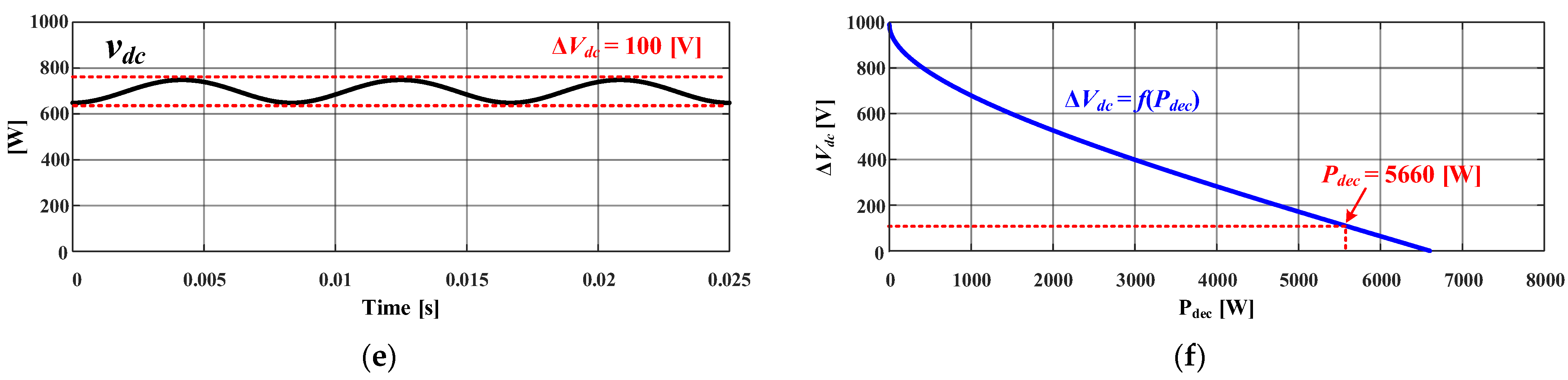
Conventional APD circuit designs set pdec equal to prip, as illustrated in Figure 2. Consequently, any ripple power at the input is eliminated from the APD circuit. To reduce the size of Cdec, which occupies the largest volume in the previously designed APD circuit, one can either decrease pdec or increase the maximum voltage of vdec, as shown in (10). However, the maximum voltage of vdec is limited by the characteristics of the APD circuit and device rating limitations, so reducing pdec is the only possible solution. Nevertheless, when pdec is reduced, as Figure 6 illustrates, prip is not entirely eliminated, resulting in ripples appearing in the output DC-link voltage. These ripples can manifest as a current ripple in the final output of the OBC system.
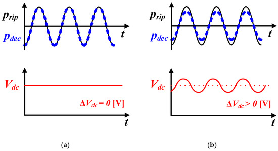
Figure 6.
DC-link voltage according to pdec. (a) Conventional design. (b) Proposed design.
Studies on the effects of the charging current ripple on lithium-ion batteries have shown the following [21,22,23]. When charging or discharging a lithium-ion battery with a sinusoidal current, the charging efficiency is lower compared to using a DC current. However, the sinusoidal current exhibits characteristics such as a slower rate of decrease in battery capacity and a lower rate of increase in internal resistance. Consequently, low-frequency ripples in the charging current do not significantly cause problems such as increased battery temperature or shortened battery life. And, because the final charging current of OBC is controlled by the DC–DC converter, the DC-link voltage has an allowable ripple considering the regulation characteristics of the DC-DC converter.
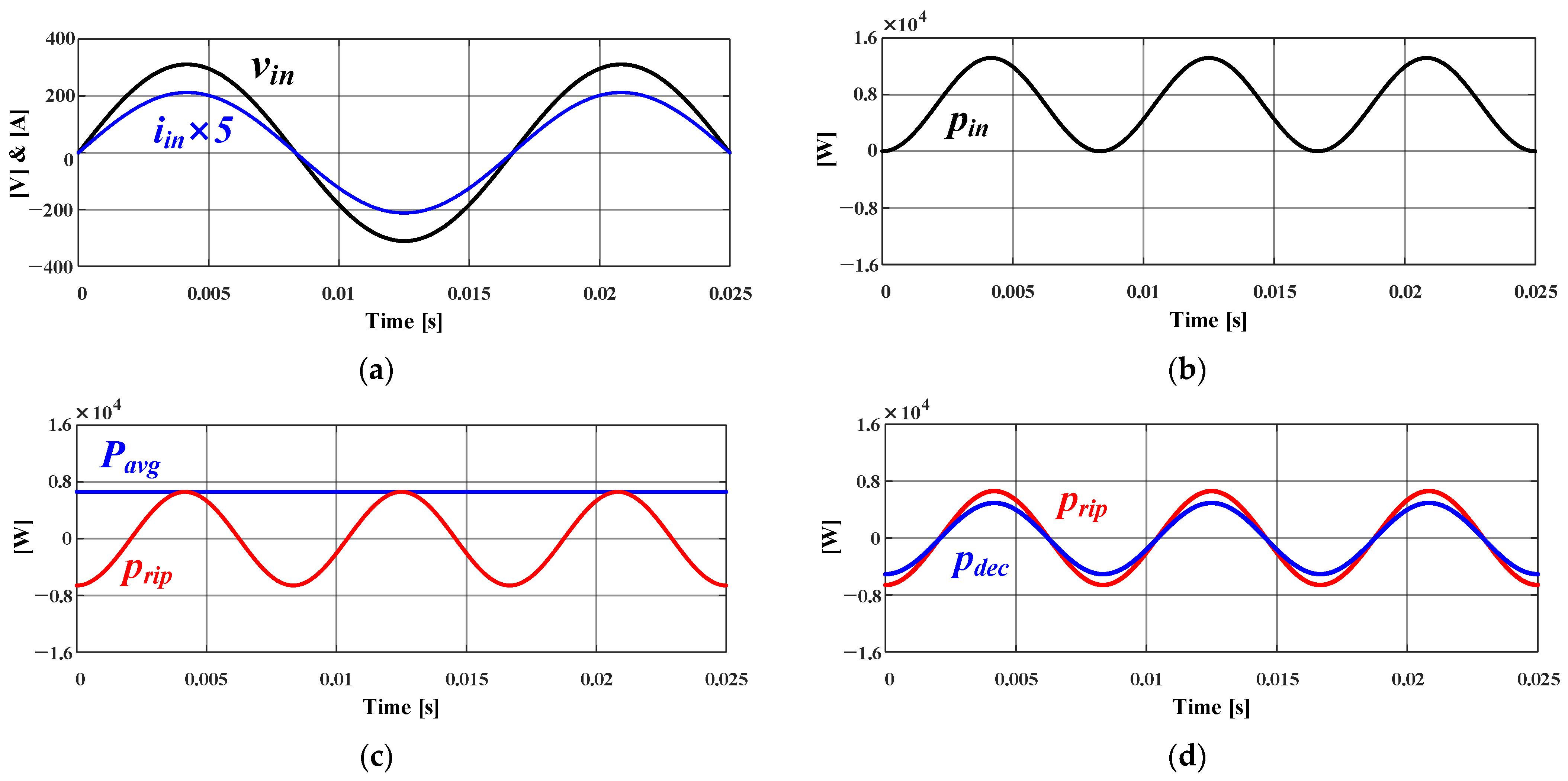
Therefore, in this study, the optimal design of Cdec is proposed under the condition that DC-link has ripple to reduce the volume of the APD circuit. Figure 7 explains the proposed design method and illustrates the process for deriving pdec from input power through input voltage and current. First, assuming unity power factor control on the input side through the PFC converter, it is expressed as shown in Figure 7a, and the voltage, current, and input power can be expressed as follows:
based on this, the input power pin is expressed, as Figure 7b illustrates, and it is divided into average power Pavg and power ripple prip, as Figure 7c illustrates, and the relational expression is derived as follows:
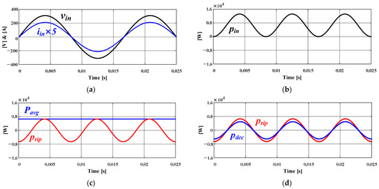
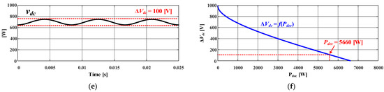
Figure 7.
Proposed APD circuit design method process. (a) Input voltage and current. (b) Input power. (c) Average power and power ripple. (d) Power ripple and decoupling power. (e) DC-link voltage. (f) Decoupling power and DC-link voltage ripple.
If only a portion of the power ripple is absorbed through the APD circuit, as Figure 7d illustrates, the DC-link voltage is expressed as a voltage with ripple, as Figure 7e shows. The output power po and voltage of the DC-link can be derived using (2), (14) and (15), assuming no losses, as follows:
Ro represents the load resistance of the final power, and using (17), the DC-link voltage ripple is as follows:
Finally, the relational expression between DC-link voltage ripple and decoupling power is as follows:
As a result, if the allowable current ripple of the OBC system is designed to be 4 A, the allowable range of DC-link voltage ripple becomes 100 V. As Figure 7f illustrates, the size of Pdec at which the DC-link voltage ripple reaches 100 V is derived as 5.66 kW. Using (10), the capacity of the final Cdec is designed to be 80 μF.
In order to verify the optimal design of Cdec proposed in this paper, the results of volume comparison analysis with the previously designed existing APD design method and PPD method are presented in Table 4. Additionally, if the PPD method also allows the same voltage ripple, the capacitance size is reduced to 270 μF. However, owing to the characteristics of electrolytic capacitors, the current allowable value is lower than that of film capacitors, so a large number of parallel capacitors are required when considering rating. Therefore, when using the electrolytic capacitor, select 720 μF, the same as the existing PPD method.
Table 4.
Comparison parameters of the conventional design and the proposed design method.
As Figure 8 shows, the proposed APD circuit design method reduces the volume by 19.7% compared to the conventional PPD method, and it is confirmed that the volume is reduced by 36.2% compared to the conventional APD circuit design method. In the case of the proposed APD circuit design, the efficiency decreases, and the cost increases due to the additional components compared to the PPD method, similar to the conventional APD circuit design method. However, it offers the advantage of addressing the volume increase issue that occurs when applying the conventional design method.
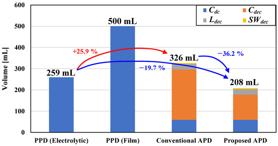
Figure 8.
Volume comparison of the proposed APD design method.
3. Verification
In order to verify the feasibility of the proposed APD circuit design method, simulation and experimental verification of the PFC converter prototype for 6.6 kW OBC are conducted. Figure 9 shows the circuit diagram of the PFC converter used for verification. Table 5 details the simulation and experimental conditions, and Table 6 provides the information about the device used.
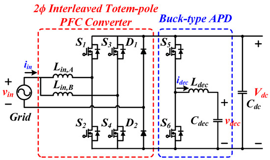
Figure 9.
The 6.6 kW PFC converter circuit for design verification.
Table 5.
Simulation and experimental verification conditions.
Table 6.
Information on devices used in the PFC converter prototype for 6.6 kW OBC.
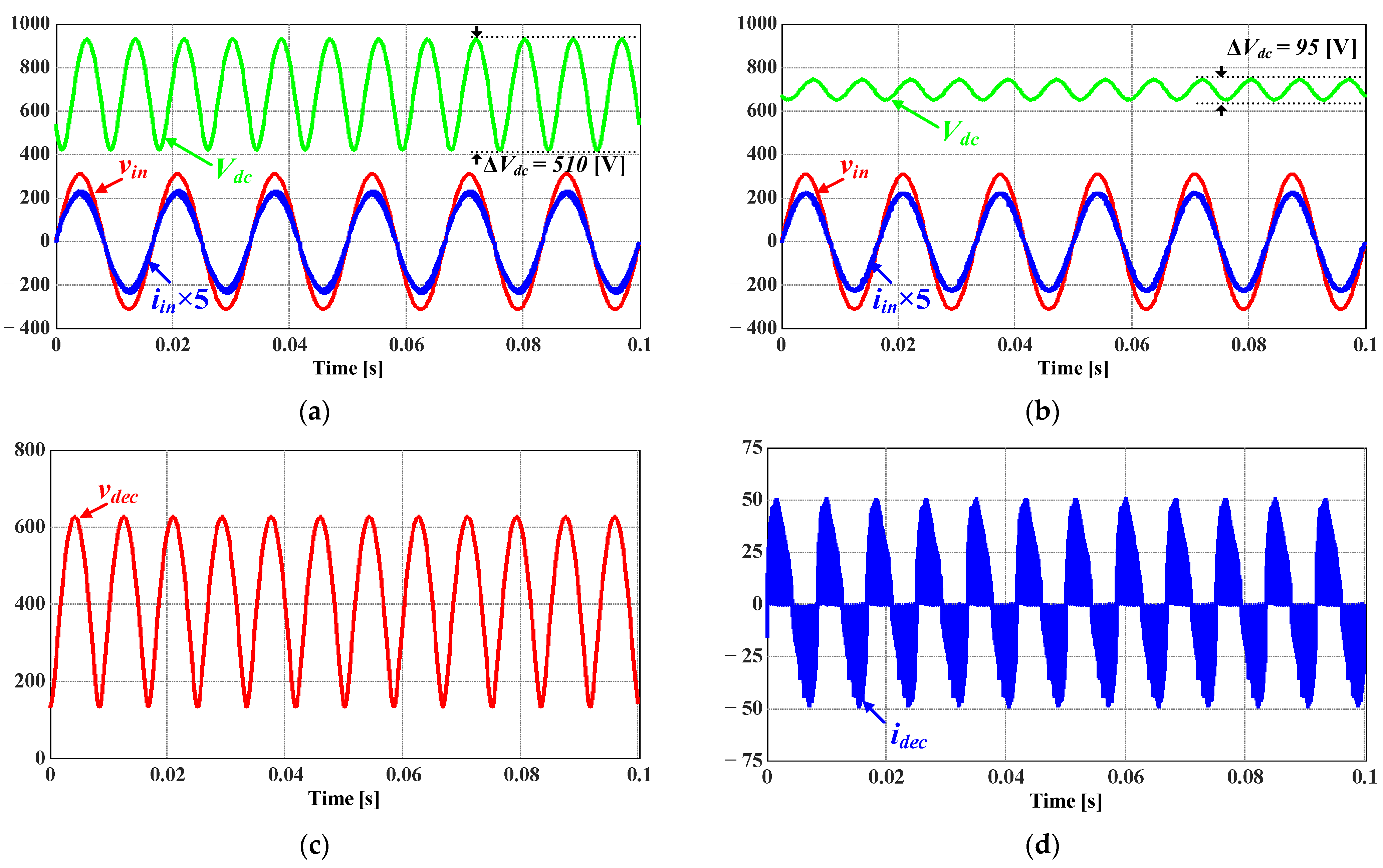
Figure 10 shows the simulation operation waveforms. Figure 10a represents the waveform when the PFC converter operates alone before the APD circuit operates. Owing to the small value DC-link capacitor value, the voltage exhibits a significant ripple of 510 V. When the APD circuit operates as shown in Figure 10b, it is confirmed that the existing large voltage ripple is reduced to less than 100 V. Figure 10c,d shows the voltage and current waveforms of the APD circuit during that time.
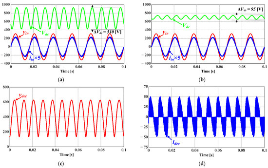
Figure 10.
Simulation verification waveform of the proposed APD design method. (a) Only PFC converter operation. (b) PFC converter and APD circuit simultaneous operation. (c) APD circuit decoupling voltage. (d) APD circuit decoupling current.
Through the above simulation results, it can be seen that the DC-link voltage ripple has a voltage ripple of approximately 100 V, similar to the design value. Figure 11 below shows the prototype of the PFC convert and APD circuit for 6.6 kW OBC. The prototype is designed with a focus on performance implementation. Figure 12 is the experimental verification result waveform.

Figure 11.
6.6 kW PFC converter and APD circuit prototype for experimental verification.
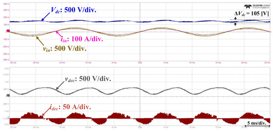
Figure 12.
Experimental waveform of the 6.6 kW PFC converter using the proposed design method.
It is confirmed that the system operates with a voltage ripple of approximately 100 V, matching the simulation results. Consequently, this validates the effectiveness of the APD circuit design method proposed in this paper.
4. Conclusions
As the use of electric vehicles increases, research on electric vehicle charging is essential to achieve high efficiency and high power density. The on-board charger (OBC) consists of a PFC converter and a DC–DC converter; the PFC converter typically uses an electrolytic capacitor, i.e., a passive power decoupling (PPD) method, to decouple the power generated through input power factor correction. However, because electrolytic capacitors have a low current rating and short lifetime, an active power decoupling (APD) method is applied to replace the electrolytic capacitors with film capacitors. Since the conventional APD method increases in volume compared to the PPD method, it is not suitable for research to achieve high power density, so a design method to achieve high power density is proposed.
To achieve an APD circuit for high power density, a volumetric comparison between the conventional APD circuit design and the PPD method is performed. Determine the effect of DC-link voltage ripple on the battery to reduce the volume of the decoupling capacitor, which occupies the largest volume. Then, the relationship between the power of the APD circuit and DC-link voltage ripple was derived. DC-link voltage ripple is obtained through OBC’s allowable current ripple, and through the capacitance derived from this, it is confirmed that volume could be reduced by 19.7% compared to the PPD method and by 36.2% compared to the conventional APD method. To verify the feasibility of the final design, experiments are performed using the PFC converter prototype for a 6.6 kW OBC. Through this, the feasibility of the proposed APD circuit design for high power density OBC is verified. As a result, it is believed that, since high power density can be achieved, more batteries can be mounted in EVs and the driving mileage can be increased, which will have a positive impact on EV sales. Additionally, the goal is to conduct experiments in the near future to confirm whether the APD circuit design method for high power density proposed in this study can be mounted on an actual OBC. These experimental tests aim to verify the feasibility of the design implementing the design proposed in this paper, thereby demonstrating the potential for developing a high power density OBC by installing the APD circuit in the actual OBC. This study is expected to be applicable to the field of new and renewable energy using APD circuits.
Author Contributions
Conceptualization, W.-J.S.; Methodology, W.-J.S.; Software, W.-J.S.; Validation, W.-J.S.; Formal analysis, W.-J.S. and B.K.L.; Investigation, W.-J.S.; Resources, B.K.L.; Data curation, W.-J.S.; Writing—original draft, W.-J.S.; Writing—review & editing, B.K.L.; Visualization, W.-J.S.; Supervision, B.K.L.; Project administration, B.K.L. All authors have read and agreed to the published version of the manuscript.
Funding
This work was supported by Korea Institute of Energy Technology Evaluation and Planning (KETEP) grant funded by the Korea government (MOTIE) (20224000000440, Sector coupling energy industry advancement manpower training program). This work was supported by Korea Institute of Energy Technology Evaluation and Planning (KETEP) grant funded by the Korea government (MOTIE) (20212020800020, Development of High Efficiency Power Converter based on Multidisciplinary Design and Optimization Platform).
Data Availability Statement
Not applicable.
Conflicts of Interest
The authors declare no conflict of interest.
References
- Iodice, P.; Fornaro, E.; Cardone, M. Hybrid Propulsion in SI Engines for New Generation Motorcycles: A Numeri-cal-Experimental Approach to Assess Power Requirements and Emission Performance. Energies 2022, 15, 6312. [Google Scholar] [CrossRef]
- Yilmaz, M.; Krein, P.T. Review of battery charger topologies, charging power levels, and infrastructure for plug-in electric and hybrid vehicles. IEEE Trans. Power Electron. 2012, 28, 2151–2169. [Google Scholar] [CrossRef]
- Khaligh, A.; D’Antonio, M. Global trends in high-power on-board chargers for electric vehicles. IEEE Trans. Veh. Technol. 2019, 68, 3306–3324. [Google Scholar] [CrossRef]
- Whitaker, B.; Barkley, A.; Cole, Z.; Passmore, B.; Martin, D.; McNutt, T.R.; Lostetter, A.B.; Lee, J.S.; Shiozaki, K. A High-Density, High-Efficiency, Isolated On-Board Vehicle Battery Charger Utilizing Silicon Carbide Power Devices. IEEE Trans. Power Electron. 2014, 29, 2606–2617. [Google Scholar] [CrossRef]
- Li, B.; Li, Q.; Lee, F.C.; Liu, Z.; Yang, Y. A High-Efficiency High-Density Wide-Bandgap Device-Based Bidirectional On-Board Charger. IEEE J. Emerg. Sel. Topics Power Electron. 2018, 6, 1627–1636. [Google Scholar] [CrossRef]
- Zhou, K.; Chen, S.-M.; Jin, N.-Z.; Sun, D.Y. Research on Single-Phase and Three-Phase Compatible Isolated On-Board Charger and Control Technology. Energies 2022, 15, 6445. [Google Scholar] [CrossRef]
- Zhao, W.H.; Shen, Y.X. Review on the research of electric vehicle on-board charger topologies. Control Eng. China 2019, 26, 29–36. [Google Scholar]
- Dai, H.C.; Ye, X.T.; Shou, Y.L.; Wang, Z.S. Research on control strategy of on-board charger (OBC) based on PFC and LLC two-level structure. Electr. Eng. 2020, 11, 38–42. [Google Scholar]
- Hu, H.; Harb, S.; Kutkut, N.; Batarseh, I.; Shen, Z.J. A Review of Power Decoupling Techniques for Microinverters With Three Different Decoupling Capacitor Locations in PV Systems. IEEE Trans. Power Electron. 2013, 28, 2711–2726. [Google Scholar] [CrossRef]
- Gautam, A.R.; Fulwani, D.M.; Makineni, R.R.; Rathore, A.K.; Singh, D. Control Strategies and Power Decoupling Topologies to Mitigate 2w-Ripple in Single-Phase Inverters: A Review and Open Challenges. IEEE Access 2020, 8, 147533–147559. [Google Scholar] [CrossRef]
- Sun, Y.; Liu, Y.; Su, M.; Xiong, W.; Yang, J. Review of Active Power Decoupling Topologies in Single-Phase Systems. IEEE Trans. Power Electron. 2016, 31, 4778–4794. [Google Scholar] [CrossRef]
- Yamaguchi, S.; Shimizu, T. A Single-Phase Power Conditioner with a Buck-Boost-Type Power Decoupling Circuit. In Proceedings of the 2014 International Power Electronics Conference (IPEC-Hiroshima 2014—ECCE ASIA), Hiroshima, Japan, 18–21 May 2014; pp. 3771–3777. [Google Scholar]
- Tang, Y.; Blaabjerg, F.; Loh, P.C.; Jin, C.; Wang, P. Decoupling of Fluctuating Power in Single-Phase Systems Through a Symmetrical Half-Bridge Circuit. IEEE Trans. Power Electron. 2015, 30, 1855–1865. [Google Scholar] [CrossRef]
- Tang, Y.; Qin, Z.; Blaabjerg, F.; Loh, P.C. A Dual Voltage Control Strategy for Single-Phase PWM Converters With Power Decoupling Function. IEEE Trans. Power Electron. 2015, 30, 7060–7071. [Google Scholar] [CrossRef]
- Larsson, T.; Ostlund, S. Active DC link Filter for Two Frequency Electric Locomotives. In Proceedings of the 1995 International Conference on Electric Railways in a United Europe, Amsterdam, The Netherlands, 27–30 March 1995; pp. 97–100. [Google Scholar]
- Han, H.; Liu, Y.; Sun, Y.; Su, M.; Xiong, W. Single-phase Current Source Converter with Power Decoupling Capability using a Series-Connected Active Buffer. IET Power Electron. 2015, 8, 700–707. [Google Scholar] [CrossRef]
- Shimizu, T.; Jin, Y.; Kimura, G. DC ripple current reduction on a single-phase PWM voltage-source rectifier. IEEE Trans. Ind. Appl. 2000, 36, 1419–1429. [Google Scholar] [CrossRef]
- Vitorino, M.A.; Correa, M.B.D.R. Compensation of DC link oscillation in single-phase VSI and CSI converters for photovoltaic grid connection. IEEE Trans. Ind. Appl. 2014, 50, 2021–2028. [Google Scholar] [CrossRef]
- Wang, R.; Wang, F.; Boroyevich, D.; Burgos, R.; Lai, R.; Ning, P.; Rajashekara, K. A High Power Density Sing-Phase PWM Rectifier With Active Ripple Energy Storage. IEEE Trans. Power Electron. 2011, 26, 1430–1443. [Google Scholar] [CrossRef]
- Nguyen, H.V.; Lee, D. Reducing the dc-Link Capacitance: Bridgeless PFC Boost Rectifier That Reduces the Second-Order Power Ripple at the dc Output. IEEE Ind. Appl. Mag. 2019, 24, 23–34. [Google Scholar] [CrossRef]
- Prasad, R.; Namuduri, C.; Kollmeyer, P. Onboard unidirectional automotive G2V battery charger using sine charging and its effect on li-ion batteries. In Proceedings of the 2015 IEEE Energy Conversion Congress and Exposition (ECCE), Montreal, CA, USA, 20–24 September 2015; pp. 6299–6305. [Google Scholar]
- Bessman, A.; Soares, R.; Vadivelu, S.; Wallmark, O.; Svens, P.; Ekstrom, H.; Lindbergh, G. Challenging Sinusoidal Ripple-Current Charging of Lithium-ion Batteries. IEEE Trans. Ind. Electron. 2018, 65, 4750–4757. [Google Scholar] [CrossRef]
- Nassary, M.; Orabi, M.; Ghoneima, M.; Aroudi, A.E.; El-Nemr, M.K. A High Current Ripple EV Battery Charger Utilizing Capacitor-less CUK Converter. In Proceedings of the 2019 IEEE Conference on Power Electronics and Renewable Energy (CPERE), Aswan, Egypt, 23–25 October 2019; pp. 232–237. [Google Scholar]


Disclaimer/Publisher’s Note: The statements, opinions and data contained in all publications are solely those of the individual author(s) and contributor(s) and not of MDPI and/or the editor(s). MDPI and/or the editor(s) disclaim responsibility for any injury to people or property resulting from any ideas, methods, instructions or products referred to in the content. |
© 2023 by the authors. Licensee MDPI, Basel, Switzerland. This article is an open access article distributed under the terms and conditions of the Creative Commons Attribution (CC BY) license (https://creativecommons.org/licenses/by/4.0/).