Article

A Self-Powered Dual-Stage Boost Converter Circuit for Piezoelectric Energy Harvesting Systems

1
Faculty of Science and Engineering, Southern Cross University, East Lismore, Lismore, NSW 2480, Australia
2
Department of Research and Development, Electronics Engineer, MYRA Corporate, Wolongbar Industrial Area, Alstonville, NSW 2477, Australia
3
Department of Electronics and Control Engineering, National Institute of Technology, Niihama College, Niihama 790-8570, Japan
*
Author to whom correspondence should be addressed.
Energies 2023, 16(5), 2490; https://doi.org/10.3390/en16052490
Submission received: 29 January 2023 / Revised: 26 February 2023 / Accepted: 28 February 2023 / Published: 6 March 2023

Abstract

:
Miniaturised piezoelectric devices are emerging energy harvesting sources that are appropriate for various implantable and wearable applications. However, these piezoelectric devices exhibit considerable internal resistance due to their internal impedance, which leads to self-start and low-energy conversion failures. This paper describes a dual-stage boost converter circuit by facilitating self-powering features and boosting the low voltage harvested by the piezoelectric devices into dc. The proposed circuit comprises conversion stages of ac-dc and dc-dc in Stages I and II, respectively. In addition, the proposed circuit does not require employing the auxiliary circuits to generate the train pulses by triggering the bidirectional switches to envelop the current being stored in Stage II and kick-start the self-powered circuit for piezoelectric energy harvesting systems. Theoretical assumptions and control strategies were tested and verified with ideal and impedance input sources. The proposed circuit could convert a low voltage of 3 Vac into 19 Vdc. The maximum attained output power by the proposed circuit was 3.61 mW. The outcome depicted that the proposed circuit boosted the low voltage and outperformed the existing literature circuits in terms of output voltage and power.

1. Introduction

The global energy demand has increased substantially in the past few decades, primarily due to the growing world population and the economic development of world-leading countries. Thus, researchers consistently develop renewable energy sources to limit the dependency on conventional energy sources. A comprehensive range of renewable energy sources is available in the environment, comprising solar [1], wind energy [2], thermal energy [3], and mechanical energy [4,5]. However, suitable energy harvesting and conversion systems are required to effectively utilise these available energy sources. One such system is piezoelectric energy harvesting, which is a mechanical vibration-based energy harvesting methodology used for harvesting electrical energy as alternating current/voltage (ac) from the ambient vibrations, which are readily available in the environment. A piezoelectric device is used to convert from mechanical energy to ac.
Apart from the device itself, a conventional piezoelectric energy harvesting system comprises three fundamental aspects: a mechanical system an electrical interface circuit [6], and a storage battery [7]. A flow diagram illustrating the piezoelectric energy harvesting system procedures is shown in Figure 1.
As the piezoelectric device is placed on a mechanical system, it harvests ac when it is subjected to excitation, while the storage devices (i.e., batteries, capacitors) require direct current/voltage (dc). Thus, the piezoelectric energy harvesting process necessitates the conversion process of ac-dc (i.e., rectification). Such conversion requires a power electronics circuit, namely, a rectifier circuit. Thus, the rectifier circuit is placed among the piezoelectric device and storage devices for rectification.
In the literature, researchers have proposed various types of rectifier circuits, including active- and passive-based power conversion circuits [8] and power conditioning circuits for piezoelectric energy harvesting [9]. These include linear, non-linear and impedance matching circuits for overcoming the shortcomings of the conversion (i.e., ac-dc) process (such as switching losses and power conversion losses), which resulted due to the piezoelectric device’s low voltage and its internal characteristics. However, the primary method is the full-bridge rectifier circuit [10], which comprises four diodes [11]. Despite its simplicity and flexibility, the full-bridge rectifier circuit possesses a significant drawback: forward voltage [12]. Thus, the output voltage (Vdc) and power through the full-bridge rectifier circuit were limited [13]. However, most power electronic devices require 3.3 Vdc. Thus, there is a necessity for a power electronic circuit that enables two features [14], namely, ac-dc and boosting low voltage into high voltage.
To address the drawbacks (i.e., the limited output voltage and power), ref. [10] proposed an H-Bridge rectifier circuit. The H-Bridge rectifier circuit comprised bidirectional switches and was proposed to transform the ac harvested by the piezoelectric device into dc by minimising forward voltage drop losses of conventional diodes in the full-bridge rectifier circuit. The intended circuit was tested successfully at high- and low-frequency vibrations. Nevertheless, the resulting outcome of the H-Bridge rectifier circuit was limited, and the boundary conditions were not well defined.
Later, to overcome this low-output voltage (Vdc), [15] modified a single-stage H-Bridge rectifier circuit into a dual-stage H-Bridge rectifier circuit. The proposed circuit successfully converted the low ac harvested by the piezoelectric device into high dc voltage (Vdc) by employing the switching process in its Stage II operation. The practical credibility of the proposed circuit was tested in two scenarios: the shaker and human motion tests. The results showed that the proposed circuit successfully charged a 1.2 Vdc, 4 mA solar battery in less than 30 min. However, the circuit experienced higher power losses due to its complexity in Stage II. In addition, the proposed circuit employed auxiliary components such as Zener diodes and ICs, which led to high conversion losses.
Another study on bridgeless rectifier circuits was conducted by [16] to minimise the diode’s forward voltage losses in the conventional bridge rectifier circuit. The proposed circuit employed a limited number of components to reduce the circuit’s power dissipation. It was tested using a series of simulations and experimental scenarios. The outcome showed that the proposed circuit achieved 1.4 times more output power than the bridge rectifier. Nevertheless, the circuit employed an auxiliary power supply to enable the switching phenomena, which made this design impractical in real-life applications.
Another methodology for achieving maximum output power is employing a non-linear system with external switches as an MOSFET (metal-oxide-field-effect-transistor), duty cycles, switching frequency, and passive electronic components, such as capacitors and inductors. A variety of non-linear approaches were proposed, including synchronous charge extraction [17], synchronized switching harvesting on inductors [18], a self-powered sequential switching harvesting on inductors [19], a single-pulse integrated circuits-based energy harvester [20], synchronous electric charge extraction [21], parallel sequencing switching harvesting on inductors, inductor-less dc-dc converter circuits [22], the sequential switching and synchronous charge extraction-based technique [23] and the synchronous charge extraction technique [24]. However, the prior proposed circuits embodied auxiliary circuits, such as diodes, transformers and bulky inductors, which are unsuitable for piezoelectric energy harvesting applications due to their high energy losses. Another approach, synchronised switching harvesting techniques, was proposed by [18,25,26]. Compared to the full-bridge rectifier circuit, the proposed circuit improved and enhanced the ac to high dc (i.e., output voltage). However, the proposed methodology adopted additional components: a polarity detector, an oscillator, diodes, a controller, logic gates and transformers. Due to this, the ac-dc conversion losses and power consumption across circuit elements are higher compared to the power generated by the piezoelectric device. In addition, the circuit required a high voltage to initiate the conversion process.
Later, [27] proposed a rectifier-less ac-dc conversion circuit by employing the synchronous process by using an inductor. A cold startup feature is introduced to the proposed circuit to achieve the optimised output from the proposed circuit. The circuit achieved a gleaning output power of 254 μW at a 0.65 mVac input voltage. However, the proposed circuitry is unsuitable, as it demands auxiliary components, such as three piezoelectric devices, three capacitors, a logic controller, an inductor and a polarity detector. Thus, the proposed circuit utilised high power and inflexibility in the PEH applications.
While the piezoelectric device generates low voltage, and the conventional full-bridge rectifier includes forward voltage issues. Most power electronic applications require 3.3 Vdc. The previously published literature highlighted that most researchers focused on rectification and boosting in their proposed circuits, which results in high power consumption and stress between the switches and parasitic components. In addition, most literature circuits require auxiliary electronic components such as polarity indicators, duty cycles, logic gates and controllers [28] to operate the circuit effectively. Therefore, a more suitable electronic circuit needs to fill the previously stated literature gap linked to boosting the low ac voltage harvested by the piezoelectric device into high dc, which results in less power consumption, less stress between the switches and no utilisation of parasitic components during the switching process.
Therefore, to avoid these drawbacks, the authors developed the two-stage conversion process circuit by garnering the combinations of the conventional voltage doubler [18,26,28,29] and the literature switching circuits [27,29,30].
The proposed dual-stage boost converter circuit employs minimal components to reduce conversion losses through a two-stage operation system. Stage I involves a voltage doubler [18,26,28,29] circuit for ac-dc conversion, while Stage II involves a dc-dc step-up voltage converter for voltage amplification. Other key benefits of the dual-stage boost converter circuit are highlighted below:
  • The proposed circuit implemented a single MOSFET switch. This reduced stress in the switching process, thus achieving a higher output voltage (Vdc) and power.
  • As highlighted in the literature, it is developed without employing complex, extraneous circuits and polarity indicators, which leads to lower conversion losses and complexity.
A comprehensive description of the dual-stage boost converter circuit is discussed in the subsequent sections.

2. Piezoelectric Energy Harvesting Circuits

This segment describes the inner features of the mechanically vibrated piezoelectric device employed in the piezoelectric energy harvesting system. Subsequently, the theoretical analysis and operations of both the voltage doubler and proposed dual-stage boost converter circuits are also explained.

2.1. Internal Circuit of a Piezoelectric Device

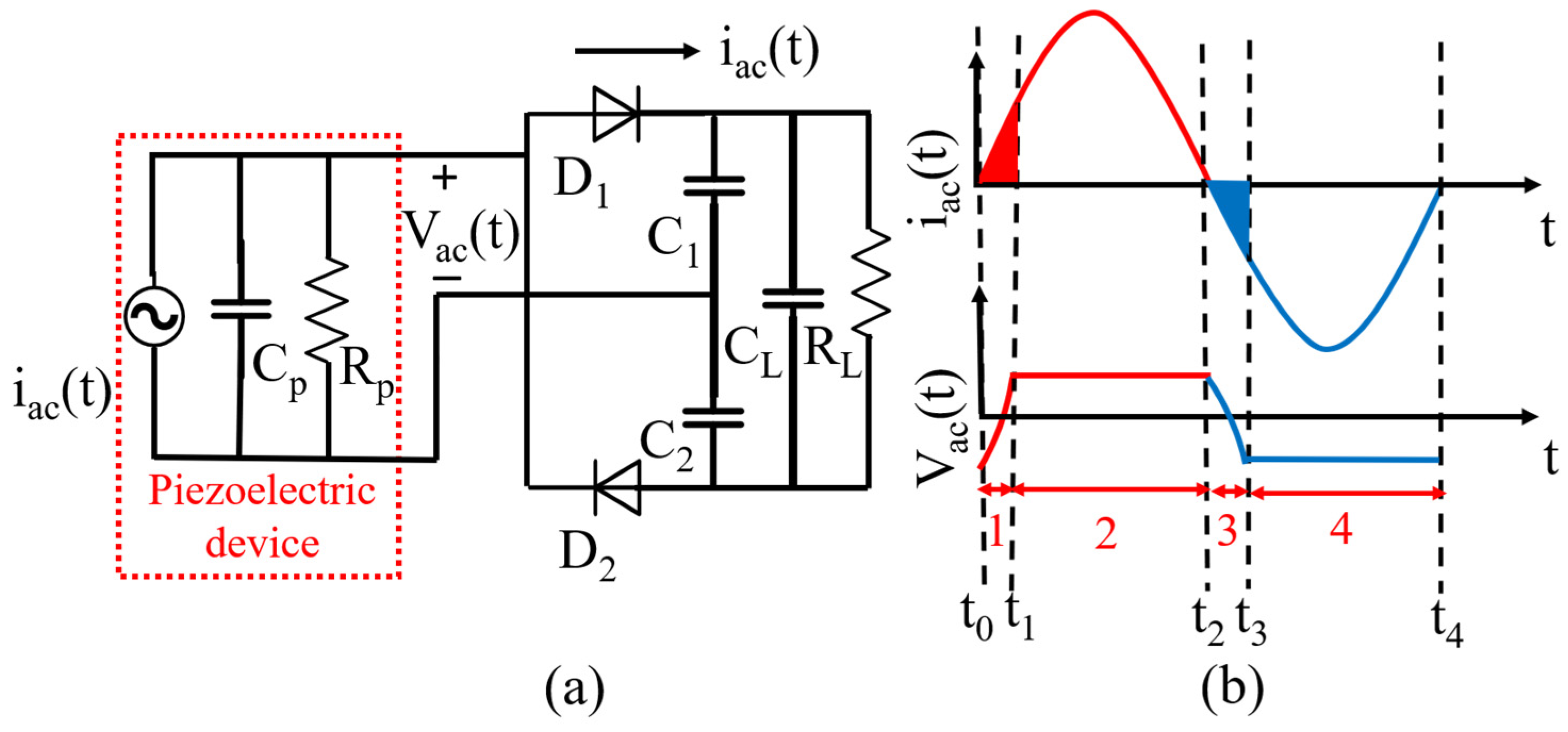
When a piezoelectric device is mechanically excited, it harvests AC voltage (Vac), comprising positive and negative half-cycles, across its electrodes. This piezoelectric device can be considered a sinusoidal current source parallel to its internal capacitor (CP) and resistor (RP). This is graphically represented in Figure 2a. Alternatively, it can also be demonstrated as a voltage source with the internal capacitor (CP) and resistor (RP) in the series configuration [31,32].
As it is considered a current source, it has to charge and discharge its internal capacitor before the piezoelectric device power flows through the electrodes. The representation of the current source and associated waveforms when the piezoelectric device is mechanically excited is represented in Figure 2. During the charging duration of the internal capacitor, no output is expected across piezoelectric device electrodes. This region is called a non-harvesting region, while the remaining period is called a harvesting period. Since the ac includes both half-cycles, the abovementioned charging and discharging procedures occur in both half-cycles. The non-harvesting region is denoted in the intervals of 1 and 3 in the time periods of t0–1 and t2–3, whereas the harvesting period is denoted in the intervals of 2 and 4 in the periods of t1–2 and t3–4 in both half-cycles, respectively [15,18,32,33]. The complete working operation of the piezoelectric device in both half-cycles is explained in Table 1.
The harvested piezoelectric device’s current (iac (t)) due to mechanical excitations can be expressed as:
i ac   ( t ) = I ac ^   sin   ( ω t )
where Îac is the magnitude of the harvested current, ω is the angular frequency, while t represents the time period.

2.2. Voltage Doubler Circuit

A voltage doubler circuit [18,18,26,28,29] and its associated current and voltage waveforms are illustrated in Figure 3. During intervals 1 and 3, the internal capacitance of the piezoelectric device gets charged in each half-cycle (positive and negative), and no current is conducted towards the load capacitor (CL). Hence, the voltage doubler circuit is OFF, which can be observed as the shaded region (Figure 3b).
However, once the internal capacitance is fully charged, the current iac (t) starts flowing towards the load capacitor (CL) and starts charging it. During this interval, the voltage doubler starts conducting, which can be observed as the non-shaded region in intervals 2 and 4 (Figure 3b).
As a result of the voltage doubler’s operation, the capacitor (CL) gets charged. The working operation of the voltage doubler circuit in both half-cycles can be observed in Table 1.

2.3. Operation Modes of the Dual-Stage Boost Convereter Circuit

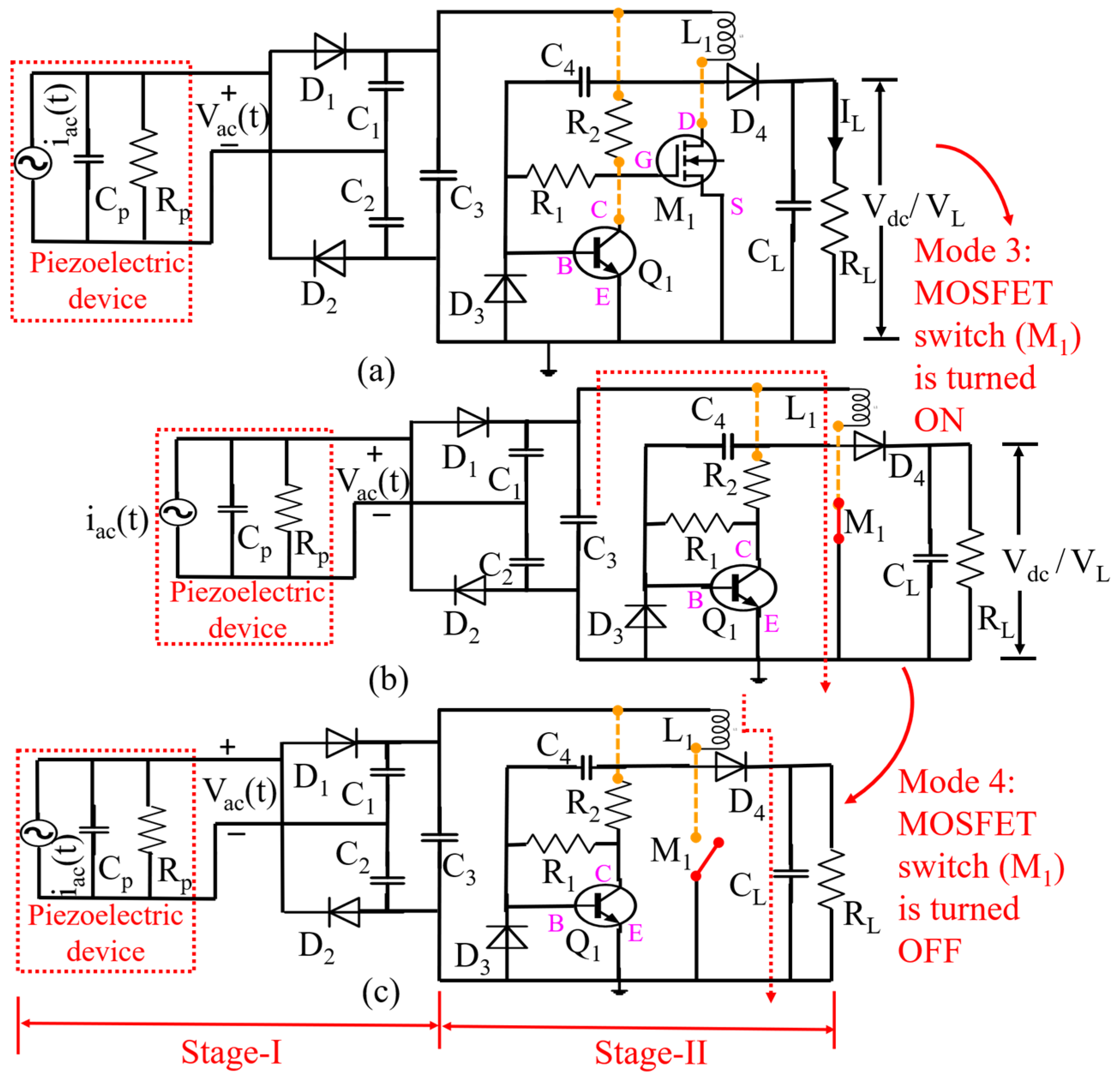
In this research, a dual-stage boost converter circuit is proposed to alleviate the drawbacks of traditional circuits. The proposed circuit in Figure 4a is designed to function in two stages (I & II) and includes four modes. Stage I involves the operation of the voltage doubler circuit for ac-dc conversion, while Stage II comprises a dc-dc step-up voltage converter to boost the stored dc voltage (Vdc) in C3 in Stage I. As the dual-stage boost converter circuit is the continuation of the voltage doubler circuit, Modes 1 and 2 (Stage I) of the dual-stage boost converter and the voltage doubler circuits are expected to be the same. As a result, the working operation of Modes 3 and 4 (Stage II) is only described in this section. It should be noted that the operations of Modes 3 and 4 (Stage II) start when Stage I’s operation fully charges the capacitor (C3).
Stage II comprises two modes of operation, 3 and 4. Mode 3 starts working when the MOSFET switch (M1) is switched ON, while Mode 4 begins when the MOSFET switch (M1) is switched OFF. The complete working operation in both modes is depicted as Figure 4b,c, respectively.
  • Mode 3: (When the MOSFET switch (M1) is ON)
Initially, the stored voltage in the capacitor (C3) passes through the inductor (L1) and flows towards the base (B) of the transistor (Q1) via the coupling capacitor (C4). It is worth noting that the transistor Q1 behaves as a voltage amplifier that amplifies a low voltage at the base (B) terminal to a higher output voltage at the collector (C) terminal.
This collector output triggers the gate (G) terminal of the MOSFET (M1) and consequently turns on M1. At this point, the accumulated voltage in the capacitor (C3) flows through the inductor (L1), leading to a gradual increase in the inductor (L1) current from zero to peak because the inductor resists a rapid change in current. The diode (D4) is reverse-biased during this time, and no current flows to the load capacitor (CL). Figure 4b illustrates the current flow during Mode 3, when the M1 is in the ON state.
  • Mode 4: (When the MOSFET switch (M1) is OFF)
When the L1 is fully saturated in this Mode, it stops the current flow towards the transistor (Q1) and turns the M1 OFF. Thus, the stored current in the L1 is freewheeled via the diode (D4) and starts charging the load capacitor (CL). Because the capacitor resists a rapid change in voltage, it charges slowly from zero to peak value. Figure 4c demonstrates the current flow during Mode 4, when the M1 is in the OFF state. A brief operation of Modes 3 and 4 is shown in Table 2.
It is worth emphasising that Stage II does not necessitate an auxiliary power source to trigger the dc-dc step-up voltage converter. Thus, switching pulses, logic gates, and integrated circuits [28] are not required to operate the proposed circuit’s MOSFET switch (M1).
As the proposed research emphasises, the piezoelectric energy harvesting systems, regarding the rectification process, the output voltage (Vdc) and the power through the proposed circuit, are chosen to validate its practical credibility. Additionally, the calculated output power of the proposed circuit is compared with an existing published literature circuit. It should be noted that the prime objective of the proposed and previously published energy harvesting circuits is to extract a higher output voltage (Vdc) and power. As a result, the output voltage (Vdc) and power are only shown in this study. The average input power (Pac) harvested by the vibrating piezoelectric device was calculated as [18,27,28]:
P ac = V Pk 2 · I Pk 2 cos φ
where I Pk and V Pk are the peak current and voltage, while φ is the phase angle between the current and voltage in the piezoelectric device.
Moreover, the output power (POUT) of the dual-stage boost converter circuit was calculated by multiplying the value of current (IL) through the load resistor (RL) and voltage (VL) across the load capacitor (CL):
POUT = VL × IL

3. Simulation Study

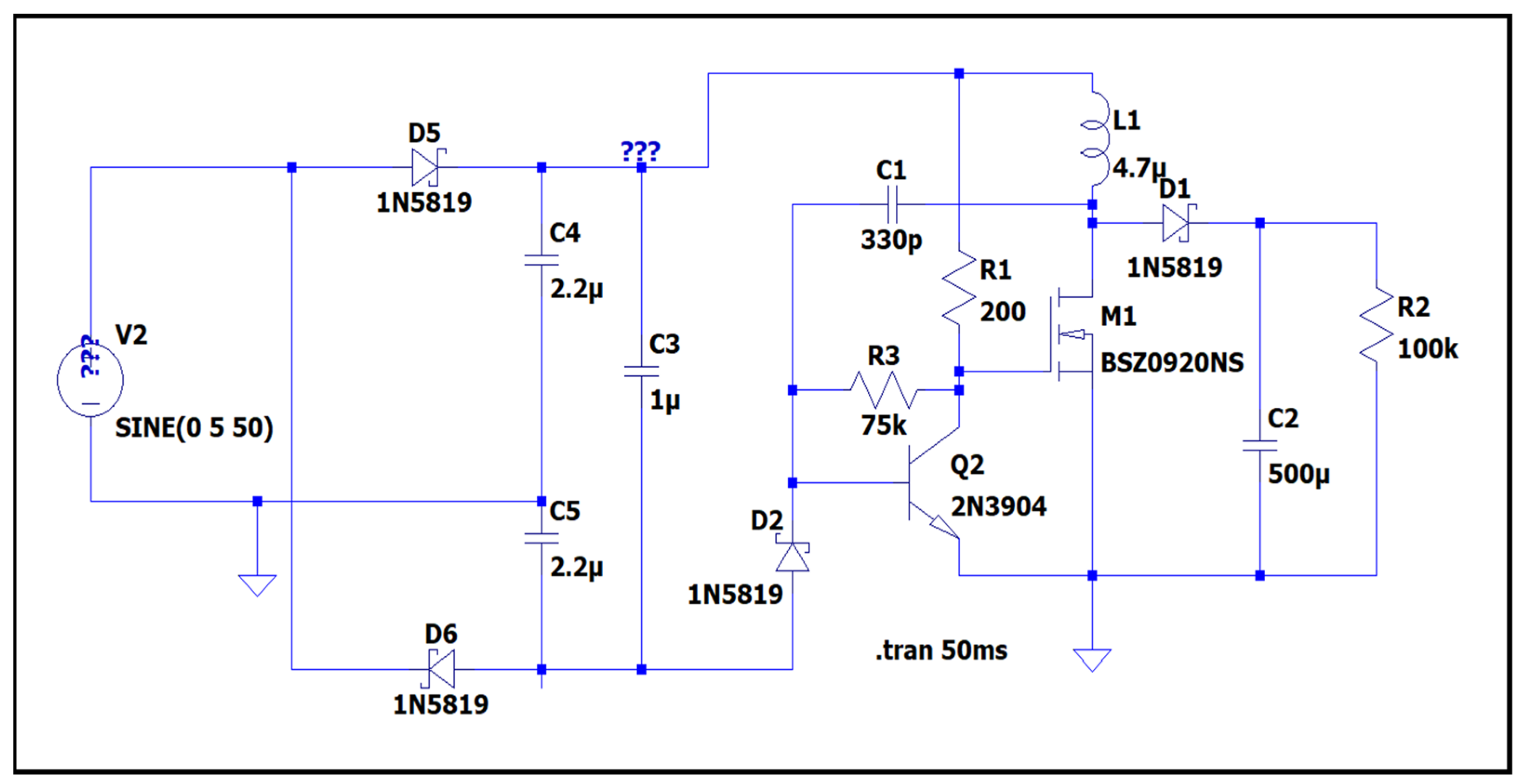
This simulation study was conducted to investigate the theoretical validation of the dual-stage boost converter circuit. LTSpice [15,18,18,22,34] software was employed in this study. Using LTSpice, an ideal ac voltage source is selected as an input and applied to the boost circuit. This input is chosen to emulate the piezoelectric device’s output for testing the proposed circuit. However, later, the ideal ac voltage source was exchanged with the piezoelectric device in the experiments.
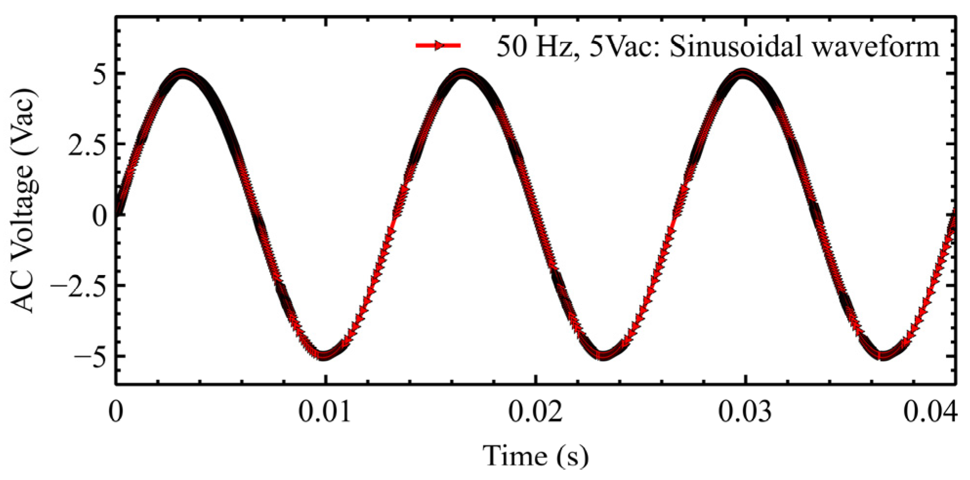
Additionally, to validate the performance capability of the proposed circuit, both ideal and piezoelectric device inputs were chosen. The acquired results from LTSpice using an ideal ac voltage source were considered proof of the concept. In LTSpice, a 5 V, 50 Hz sinusoidal waveform was chosen as the input ideal ac voltage source. The simulation model of the proposed circuit at 5 Vac and a 50 Hz frequency is depicted in Figure 5.
The adopted electronic components and their parameters for the proposed circuit are described in Table 3.
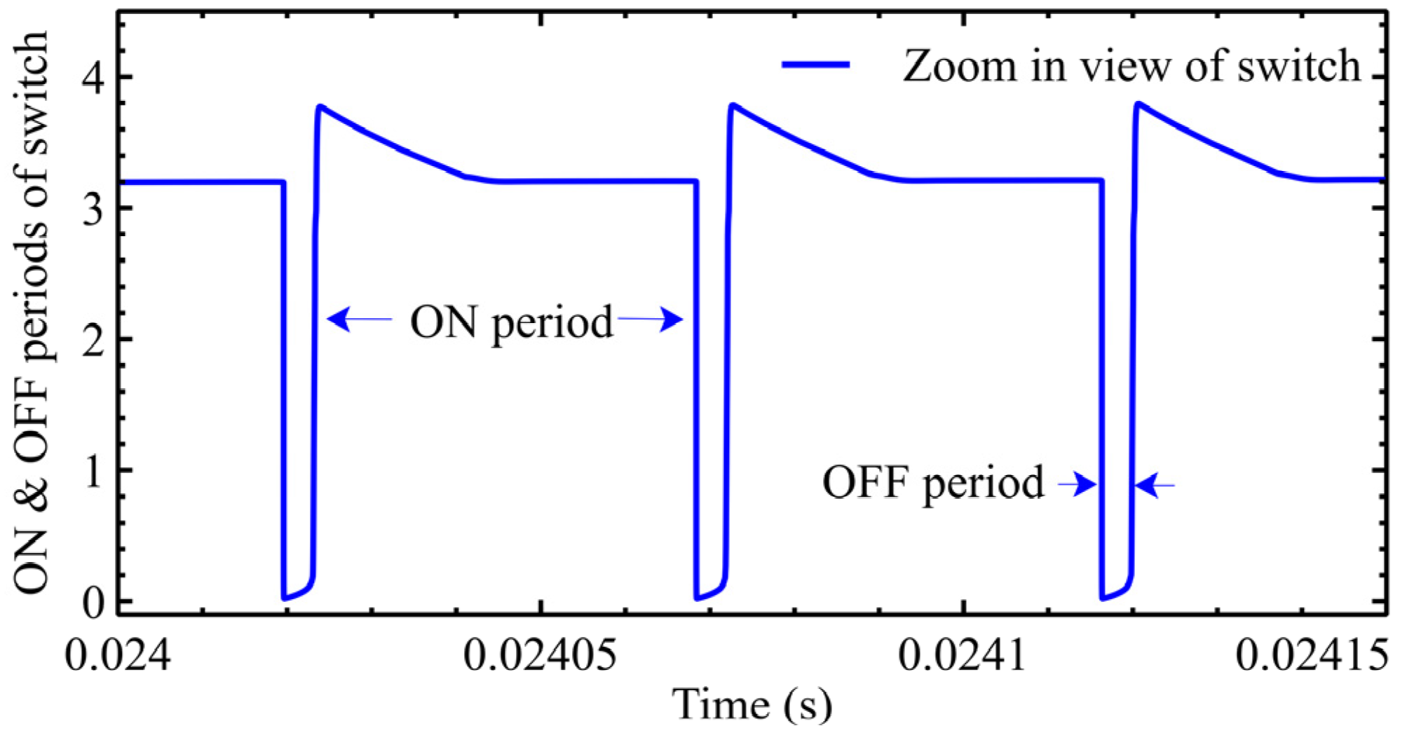
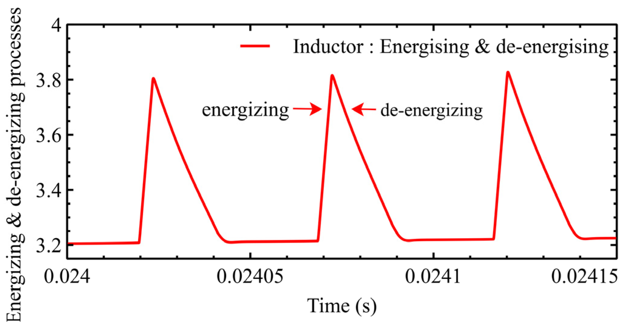
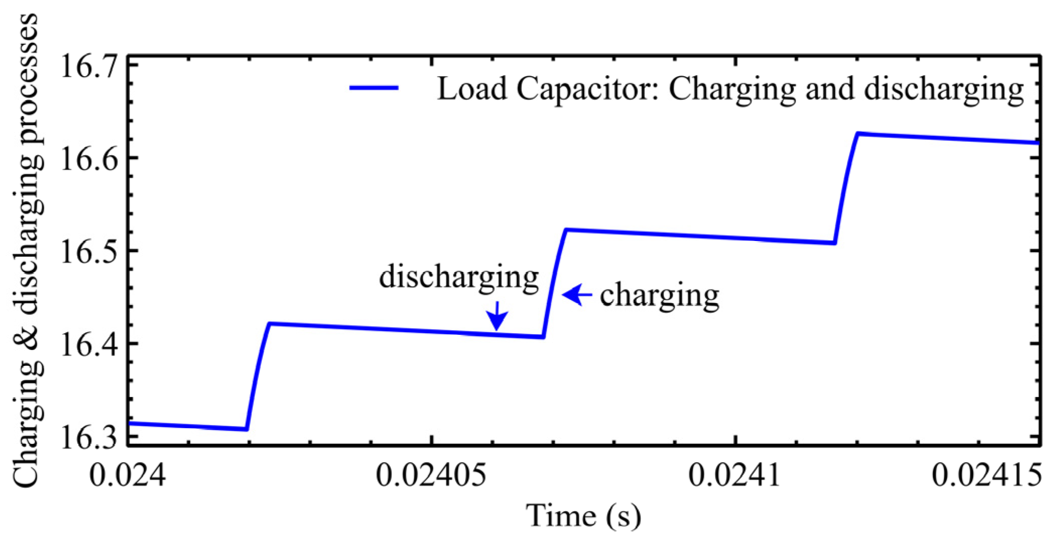
Figure 6 demonstrates the adopted ideal ac voltage source. A comprehensive zoom-in view of the ON and OFF periods of the MOSFET switch (M1), as discussed in section II, is illustrated in Figure 7. As a result of MOSFET switching, the inductor gets energised and de-energised, which is depicted in Figure 8. In addition, the charging and discharging of load capacitors (CL) are illustrated within the context of Figure 9.

4. Experimental Study

In both testing scenarios (at a constant voltage (Test 1) and a constant frequency (Test 2)), an MFC-M2814-P2 patch (37 mm × 17 mm × 0.180 mm, internal capacitance: 30.79 nF) was used as a piezoelectric device. The piezoelectric device patch was glued on the surface of an aluminium cantilevered beam (Dimensions: 205 mm × 20 mm × 1 mm) at the fixed end, while two permanent magnets were coupled on the free end, acting as a proof mass. A voltmeter and ammeter [CD 771] were used to measure the output voltage (Vdc) and current, respectively.
To generate an input ac voltage (Vac) from the piezoelectric device, a function generator (Agilent 33210A) was utilised, which was attached to the power amplifier (2706, B&K Agilent). This combination boosted the ac voltage (Vac) from the piezoelectric device before applying it to the mechanical shaker (APS-113). This mechanical shaker induced harmonic vibrations based on the given input amplitude and frequency to shake the cantilevered beam incorporated with a piezoelectric device. The frequency and amplitude at which the piezoelectric device harvested mechanical vibrations were collectively adjusted through the function generator and power amplifier. When the harvested ac voltage (Vac) from the vibrating piezoelectric device was supplied to the dual-stage boost converter circuit, it conducted Stage I (ac-dc) and Stage II (dc-dc) operations.
In Tests 1 and 2, the harvested AC voltage (Vac) from the piezoelectric device through the proposed circuit was investigated using varying input parameters, as highlighted in Table 4. In Test 1, the proposed circuit was tested at a constant input voltage under varying frequencies. In Test 2, the proposed circuit was analysed at a constant frequency under a variable input voltage. The generated output voltage (Vdc) through the dual-stage boost converter circuit was stored in CL in both testing scenarios. In addition, each load resistor (RL) was connected in parallel, and the output was measured using a multimeter. An experimental setup of the proposed circuit is depicted in Figure 10.

4.1. Test 1: Varying Excitation Frequency under a Constant Input Voltage

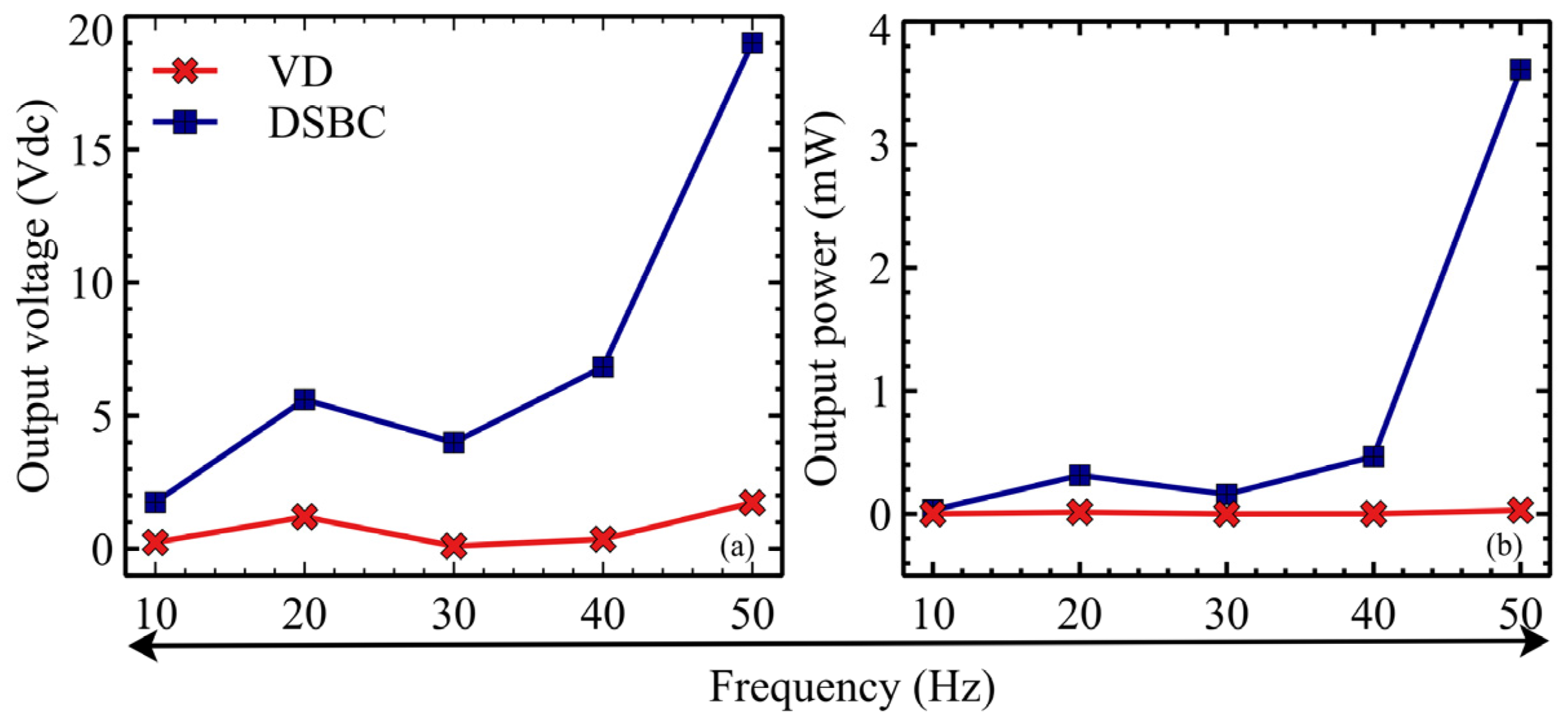
The output voltage (Vdc) and power obtained from Test 1 are highlighted in Figure 11a,b, respectively. The dotted line represents the voltage doubler circuit, while the solid line indicates the dual-stage boost converter circuit. The output voltage (Vdc) and power from both the proposed and voltage doubler circuits are compared under varied input frequencies (10–50 Hz) and load resistances (RL).
By analysing Figure 11a, it can be regarded that the output voltage (Vdc) increases substantially by increasing the value of load resistances from 100 KΩ to 910 KΩ. Irrespective of the excitation frequency, the proposed circuit yielded a higher output voltage (Vdc) than the voltage doubler circuit under a constant input voltage (3 Vac). It is to be noted that the proposed circuit achieved a higher output voltage (Vdc) at a higher load resistance (RL).
Initially, a 3 Vac input voltage was given to the proposed circuit at an excitation frequency of 10 Hz. Consequently, Stage I conducted ac-dc conversion, and the output voltage (Vdc) was stored in the capacitor (C3) (Figure 4a). It should be noted that Stage II does not operate unless Stage I fully charges the capacitor (C3). When it is fully charged, it stimulates the current flow in Stage II.
The stored charge in the C3 passed through the L1 and flowed towards the base of the transistor (Q1) through the coupling capacitor (C4). This transistor (Q1) behaved as a Common Emitter voltage amplifier, amplifying any input voltage at the base terminal to a higher output voltage at the collector terminal. This output at the collector terminal triggered the MOSFET’s switch (M1) gate terminal, allowing for the current flow source from the drain and energising the inductor (L1).
Once the inductor (L1) is fully saturated, it stops the current flow to the transistor (Q1). Consequently, the MOSFET switch (M1) turned OFF. Thus, the stored charge in the inductor (L1) forward-biased the diode (D4) and started charging the load capacitor (CL). Afterwards, each load resistor from R1 to R4 was connected in parallel with the load capacitor (CL), and the respective output voltages (Vdc) were measured.
Later, the remaining excitation frequencies (20–40 Hz) were applied under a similar input voltage (3 Vac), and the resulting output voltage (Vdc) for each load resistor (RL) (R1–R4) was measured (Figure 11a). In addition, the output power was calculated using Equation (3) by measuring the voltage (VL) across the load capacitor (CL) and the current through the load resistor (RL). Figure 11b shows the output power under various excitation frequencies and a fixed input voltage. It is noted that the output power shows a different trend as compared to the output voltage (Vdc) at various load resistances (RL). This is because the harvested current through each load resistor (RL) was different. Thus, the calculated output power was dissimilar.
By further examining Figure 11, it can be observed that the excitation frequency substantially impacts the proposed circuit’s overall performance. The output voltage (Vdc) and power were elevated at higher frequencies. The output voltage (Vdc) and power at different excitation frequencies (10–50 Hz) with a constant input ac voltage (Vac) are depicted in Figure 12a,b, respectively. It should be noted that the proposed circuit yielded a higher output voltage (Vdc) and power under higher excitation frequencies. This is due to the reason that, at higher frequencies, the capacitive reactance of the piezoelectric device decreases. As a result, the piezoelectric device generates a higher ac voltage (Vac), leading to a higher output voltage (Vdc) and power.
It should be noted that the prime goal of this research is to validate the performance of the proposed circuit to track the optimal points and power dependency on the frequency under varying load resistances and the attainment of the maximum output voltage (Vdc) and power at a frequency of 50 Hz at 3 Vac.

4.2. Test 2: Varying Input Voltage under a Constant Excitation Frequency

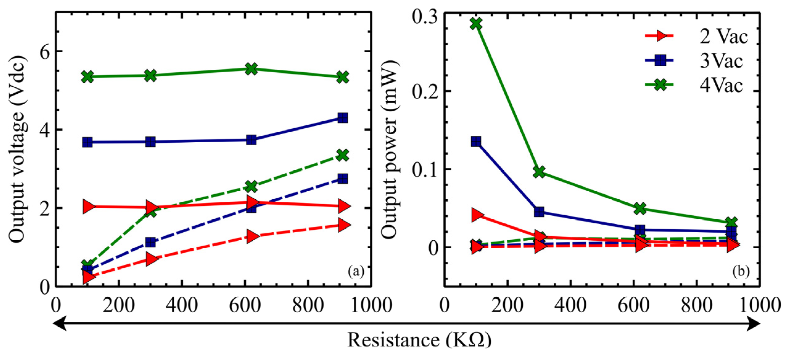
In this testing scenario, the dual-stage boost converter and the voltage doubler circuits were further analysed under varying input voltages (Vac). The frequency was kept constant at 1 Hz. The vibrating piezoelectric device’s ac voltage (Vac) was chosen from 1 Vac to 5 Vac. A voltmeter was utilised to measure the harvested Vac from the vibrating piezoelectric device before applying it to the proposed circuit. A detailed summary of the different investigated parameters is reported in Table 4. Figure 13a,b represent the results of the output voltage (Vdc) and power from Test 2. The dotted line represents the voltage doubler circuit, while the solid line signifies the proposed circuit.
Initially, 1 Vac from a vibrating piezoelectric device was applied across the proposed circuit. As the input ac voltage (Vac) was more significant than the threshold voltage of the transistor (Q1) and MOSFET (M1) switches, the proposed circuit started functioning, as explained in section IV-B. This resulted in achieving 0.36 Vdc, which was stored in the load capacitor (CL). Similarly, when 3 Vac and 4 Vac were applied to the proposed circuit, 3.64 Vdc and 5.35 Vdc were achieved and stored in the load capacitor (CL). It should be noted that a higher output voltage (Vdc) was achieved at a higher ac voltage (Vac) because when the applied ac voltage (Vac) increased, the drain to the source resistance path in the mosfet switch decreased [15,15,20,28,30]. Figure 11a illustrates the output voltages (Vdc) from both circuits under various input ac voltages (Vac). It can be observed that the proposed circuit yielded a higher output voltage (Vdc) compared to the voltage doubler circuit at similarly applied ac voltages (Vac).
Next, the output power was measured at the load capacitor (CL) using Equation (3). The relation between the input ac voltage (Vac) and the output power at a 1 Hz excitation frequency is depicted in Figure 13b. A higher output power was accumulated at the load capacitor (CL) with an input voltage of 4Vac, while the least power was detected at 2 Vac at the load capacitor (CL) using the proposed circuit. It can be noticed that, at higher input ac voltages (Vac), the resistance in the drain to the source path of the MOSFET switch (M1) was decreased. As a result, a higher output voltage (Vdc) is gathered in the load capacitor (CL), thus increasing the output power.
It was observed that the output voltage (Vdc) increased with the enhancing load resistance (100–910 KΩ). The highest output voltage (Vdc) is obtained at 910 KΩ, while the lowest was observed at 100 KΩ. The behaviour was persistent for all input AC voltages (Vac) and complied with Ohm’s law (Figure 13a). On the contrary, the behaviour of the output power with the increasing load resistance was different (Figure 13b). This might be due to the reason that the current flowing at different load resistors is different. Thus, the calculated output power was not consistent.
By further examining Figure 13, it is highlighted that the extent of the applied input ac voltage (Vac) substantially impacts the proposed circuit’s overall performance. At a higher Vac, the output voltage (Vdc) and power became higher as well. The output voltage (Vdc) and power at different input voltages (1 Vac–5 Vac) over a 1 Hz excitation frequency and at a 100 KΩ load resistor are depicted in Figure 14a,b, respectively.
It is worth mentioning that the proposed circuit outperformed the voltage doubler circuit, where the output voltage (Vdc) and power generated by the proposed circuit are higher than the voltage doubler circuit in all scenarios. Considering that the principal objective of this study is to enhance the output voltage (Vdc) and power, this is accomplished by using the proposed circuit. Table 5 lists the generated output power of similar circuits published in the previous literature.
It was found that the proposed circuit outperformed various previously published literature circuits regarding the output voltage and power.

5. Conclusions

In this research, a self-powered dual-stage boost converter circuit was proposed and thoroughly studied to boost the low ac voltage generated by the piezoelectric device into dc in piezoelectric energy harvesting systems. The dual-stage boost converter circuit integrated a voltage doubler and a dc-dc boost converter as two stages (I & II) to function in both ac-dc and dc-dc conversion processes. In addition, it avoided the need for an expensive auxiliary circuit for effective operations. Due to using a single MOSFET, it reduced the stress across the switching process. In addition, the practical capability of the dual-stage boost converter circuit was verified using simulation and laboratory-based experiments. The proposed prototype converted a 3 Vac and 50 Hz input ac voltage (Vac) to 19 Vdc and achieved an output power of 3.61 mW under Test 1. Moreover, it converted a 5 Vac and 1 Hz input ac voltage (Vac) to 10.9 Vdc and achieved an output power of 0.396 mW under Test 2. The proposed circuit is proven to be exceptional compared to the existing literature circuits. The proposed circuit is suitable for the efficient energy conversion of vibrating piezoelectric devices for low-power portable/wireless devices. It is noted that the proposed circuit is limited to low-voltage applications only. For ultra-low voltages, the proposed prototype is not suitable, as the input voltage will be dissipated across circuit components, and there will be no output at the load. For future work, the modification of the dual-stage boost converter circuit to incorporate the non-linear process is recommended.

Author Contributions

Conceptualization, A.H.; methodology, A.H.; software, A.H.; validation, A.H.; formal analysis, A.H.; investigation, A.H.; resources, A.H.; data curation, A.H. and M.E.; writing—original draft preparation, A.H.; writing—review and editing, A.H., M.E. and A.M.T.; visualization, A.H.; supervision, M.E., A.M.T. and M.D.; project administration, M.E., A.M.T. and M.K.; funding acquisition, Not Applicable. All authors have read and agreed to the published version of the manuscript.

Funding

The work is supported by Southern Cross University, Faculty of Science and Engineering, Lismore, NSW, 2480.

Data Availability Statement

Data is available on request due to privacy and restrictions.

Conflicts of Interest

The authors declare no conflict of interest.

References

  1. Rand, B.P.; Genoe, J.; Heremans, P.; Poortmans, J. Solar cells utilizing small molecular weight organic semiconductors. Prog. Photovolta. Res. Appl. 2007, 15, 659–676. [Google Scholar] [CrossRef] [Green Version]
  2. De Broe, A.M.; Drouilhet, S.; Gevorgian, V. A peak power tracker for small wind turbines in battery charging applications. IEEE Trans. Energy Convers. 1999, 14, 1630–1635. [Google Scholar] [CrossRef]
  3. Sebald, G.; Pruvost, S.; Guyomar, D. Energy harvesting based on Ericsson pyroelectric cycles in a relaxor ferroelectric ceramic. Smart Mater. Struct. 2007, 17, 015012. [Google Scholar] [CrossRef]
  4. Edla, M.; Lim, Y.Y. An improved piezoelectric energy harvesting circuit for reducing the internal loss. In Proceedings of the 83rd Researchfora International Conference, New Delhi, India, 29 January 2020; pp. 4–8. [Google Scholar]
  5. Izadgoshasb, I.; Lim, Y.Y.; Tang, L.; Padilla, R.V.; Tang, Z.S.; Sedighi, M. Improving efficiency of piezoelectric based energy harvesting from human motions using double pendulum system. Energy Convers. Manag. 2019, 184, 559–570. [Google Scholar] [CrossRef]
  6. Wu, L.; Kang, W.; Xie, M.; Zhu, P. A self-powered multi-input bridgeless series-SSHI circuit for piezoelectric energy harvesting. In Proceedings of the 2021 IEEE International Symposium on Circuits and Systems (ISCAS), Daegu, Republic of Korea, 22–28 May 2021; pp. 1–4. [Google Scholar]
  7. Edla, M.; Lim, Y.Y.; Padilla, R.V.; Deguchi, M. An improved rectifier circuit for piezoelectric energy harvesting from human motion. Appl. Sci. 2021, 11, 2008. [Google Scholar] [CrossRef]
  8. Szarka, G.D.; Stark, B.H.; Burrow, S.G. Review of power conditioning for kinetic energy harvesting systems. IEEE Trans. Power Electron. 2011, 27, 803–815. [Google Scholar] [CrossRef]
  9. Chalasani, S.; Conrad, J.M. A survey of energy harvesting sources for embedded systems. In Proceedings of the IEEE Southeastcon 2008, Huntsville, AL, USA, 3–6 April 2008; pp. 442–447. [Google Scholar]
  10. Edla, M.; Lim, Y.Y.; Deguchi, M.; Padilla, R.V.; Izadgoshasb, I. An improved self-powered H-bridge circuit for voltage rectification of piezoelectric energy harvesting system. IEEE J. Electron Devices Soc. 2020, 8, 1050–1062. [Google Scholar] [CrossRef]
  11. Cheng, S.; Jin, Y.; Rao, Y.; Arnold, D.P. A bridge voltage doubler AC/DC converter for low-voltage energy harvesting applications. In Proceedings of the PowerMEMS 2009, Washington, DC, USA, 1–4 December 2009; pp. 25–28. [Google Scholar]
  12. Du, S.; Amaratunga, G.A.; Seshia, A.A. A cold-startup SSHI rectifier for piezoelectric energy harvesters with increased open-circuit voltage. IEEE Trans. Power Electron. 2018, 34, 263–274. [Google Scholar] [CrossRef]
  13. Edla, M.; Lim, Y.Y.; Mikio, D.; Padilla, R.V. A single-stage rectifier-less boost converter circuit for piezoelectric energy harvesting systems. IEEE Trans. Energy Convers. 2021, 37, 505–514. [Google Scholar] [CrossRef]
  14. Edla, M.; Lim, Y.Y.; Deguchi, M.; Padilla, R.V. A Novel Discontinuous Mode Piezoelectric Energy Harvesting Circuit for Low-Voltage Applications. In Proceedings of the 2021 31st Australasian Universities Power Engineering Conference (AUPEC), Perth, Australia, 26–30 September 2021; pp. 1–5. [Google Scholar]
  15. Edla, M.; Lim, Y.Y.; Padilla, R.V.; Mikio, D. Design and Application of a Self-Powered Dual-Stage Circuit for Piezoelectric Energy Harvesting Systems. IEEE Access 2021, 9, 86954–86965. [Google Scholar] [CrossRef]
  16. Srinivasan, R.; Mangalanathan, U.; Gandhi, U.; Karlmarx, L.R. Bridgeless active rectifier for piezoelectric energy harvesting. IET Circuits Devices Syst. 2019, 13, 1078–1085. [Google Scholar] [CrossRef]
  17. Dini, M.; Romani, A.; Filippi, M.; Tartagni, M. A nanopower synchronous charge extractor IC for low-voltage piezoelectric energy harvesting with residual charge inversion. IEEE Trans. Power Electron. 2015, 31, 1263–1274. [Google Scholar] [CrossRef]
  18. Du, S.; Jia, Y.; Zhao, C.; Amaratunga, G.A.; Seshia, A.A. A nail-size piezoelectric energy harvesting system integrating a MEMS transducer and a CMOS SSHI circuit. IEEE Sens. J. 2019, 20, 277–285. [Google Scholar] [CrossRef] [Green Version]
  19. Eltamaly, A.M.; Addoweesh, K. Self Power SSHI Circuit for Piezoelectric Energy Harvester. U.S. Patent 9,548,680, 17 January 2017. [Google Scholar]
  20. Lee, M.; Yang, J.; Park, M.-J.; Jung, S.-Y.; Kim, J. Design and analysis of energy-efficient single-pulse piezoelectric energy harvester and power management IC for battery-free wireless remote switch applications. IEEE Trans. Circuits Syst. I Regul. Pap. 2017, 65, 366–379. [Google Scholar] [CrossRef]
  21. Lefeuvre, E.; Badel, A.; Brenes, A.; Seok, S.; Woytasik, M.; Yoo, C.-S. Analysis of piezoelectric energy harvesting system with tunable SECE interface. Smart Mater. Struct. 2017, 26, 035065. [Google Scholar] [CrossRef]
  22. Pollet, B.; Despesse, G.; Costa, F. A new non-isolated low-power inductorless piezoelectric dc–dc converter. IEEE Trans. Power Electron. 2019, 34, 11002–11013. [Google Scholar] [CrossRef]
  23. Xia, H.; Xia, Y.; Shi, G.; Ye, Y.; Wang, X.; Chen, Z.; Jiang, Q. A self-powered S-SSHI and SECE hybrid rectifier for PE energy harvesters: Analysis and experiment. IEEE Trans. Power Electron. 2020, 36, 1680–1692. [Google Scholar] [CrossRef]
  24. Xia, H.; Xia, Y.; Ye, Y.; Qian, L.; Shi, G.; Chen, R. Analysis and simulation of synchronous electric charge partial extraction technique for efficient piezoelectric energy harvesting. IEEE Sens. J. 2018, 18, 6235–6244. [Google Scholar] [CrossRef]
  25. Liang, J.; Liao, W.-H. Improved design and analysis of self-powered synchronized switch interface circuit for piezoelectric energy harvesting systems. IEEE Trans. Ind. Electron. 2011, 59, 1950–1960. [Google Scholar] [CrossRef]
  26. Tabesh, A.; Fréchette, L.G. A low-power stand-alone adaptive circuit for harvesting energy from a piezoelectric micropower generator. IEEE Trans. Ind. Electron. 2009, 57, 840–849. [Google Scholar] [CrossRef] [Green Version]
  27. Shareef, A.; Goh, W.L.; Narasimalu, S.; Gao, Y. A rectifier-less AC–DC interface circuit for ambient energy harvesting from low-voltage piezoelectric transducer array. IEEE Trans. Power Electron. 2018, 34, 1446–1457. [Google Scholar] [CrossRef]
  28. Lefeuvre, E.; Audigier, D.; Richard, C.; Guyomar, D. Buck-boost converter for sensorless power optimization of piezoelectric energy harvester. IEEE Trans. Power Electron. 2007, 22, 2018–2025. [Google Scholar] [CrossRef]
  29. Kushino, Y.; Koizumi, H. Piezoelectric energy harvesting circuit using full-wave voltage doubler rectifier and switched inductor. In Proceedings of the 2014 IEEE Energy Conversion Congress and Exposition (ECCE), Pittsburgh, PA, USA, 14–18 September 2014; pp. 2310–2315. [Google Scholar]
  30. Rashid, M.H. Power Electronics Handbook; Butterworth-Heinemann: Oxford, UK, 2017. [Google Scholar]
  31. Erturk, A.; Inman, D.J. Piezoelectric Energy Harvesting; John Wiley & Sons: Hoboken, NJ, USA, 2011. [Google Scholar]
  32. Lu, S.; Boussaid, F. A highly efficient P-SSHI rectifier for piezoelectric energy harvesting. IEEE Trans. Power Electron. 2015, 30, 5364–5369. [Google Scholar] [CrossRef] [Green Version]
  33. Eltamaly, A.M.; Addoweesh, K.E. A novel self-power SSHI circuit for piezoelectric energy harvester. IEEE Trans. Power Electron. 2016, 32, 7663–7673. [Google Scholar] [CrossRef]
  34. Mikkelsen, J.H. Ltspice—An Introduction; Technical Report; Institute of Electronic Systems, Aalborg University: Aalborg, Denmark, 2005. [Google Scholar]
  35. Kwon, D.; Rincón-Mora, G.A. A 2-µm BiCMOS rectifier-free AC–DC piezoelectric energy harvester-charger IC. IEEE Trans. Biomed. Circuits Syst. 2010, 4, 400–409. [Google Scholar] [CrossRef]
  36. Romani, A.; Filippi, M.; Tartagni, M. Micropower design of a fully autonomous energy harvesting circuit for arrays of piezoelectric transducers. IEEE Trans. Power Electron. 2013, 29, 729–739. [Google Scholar] [CrossRef]
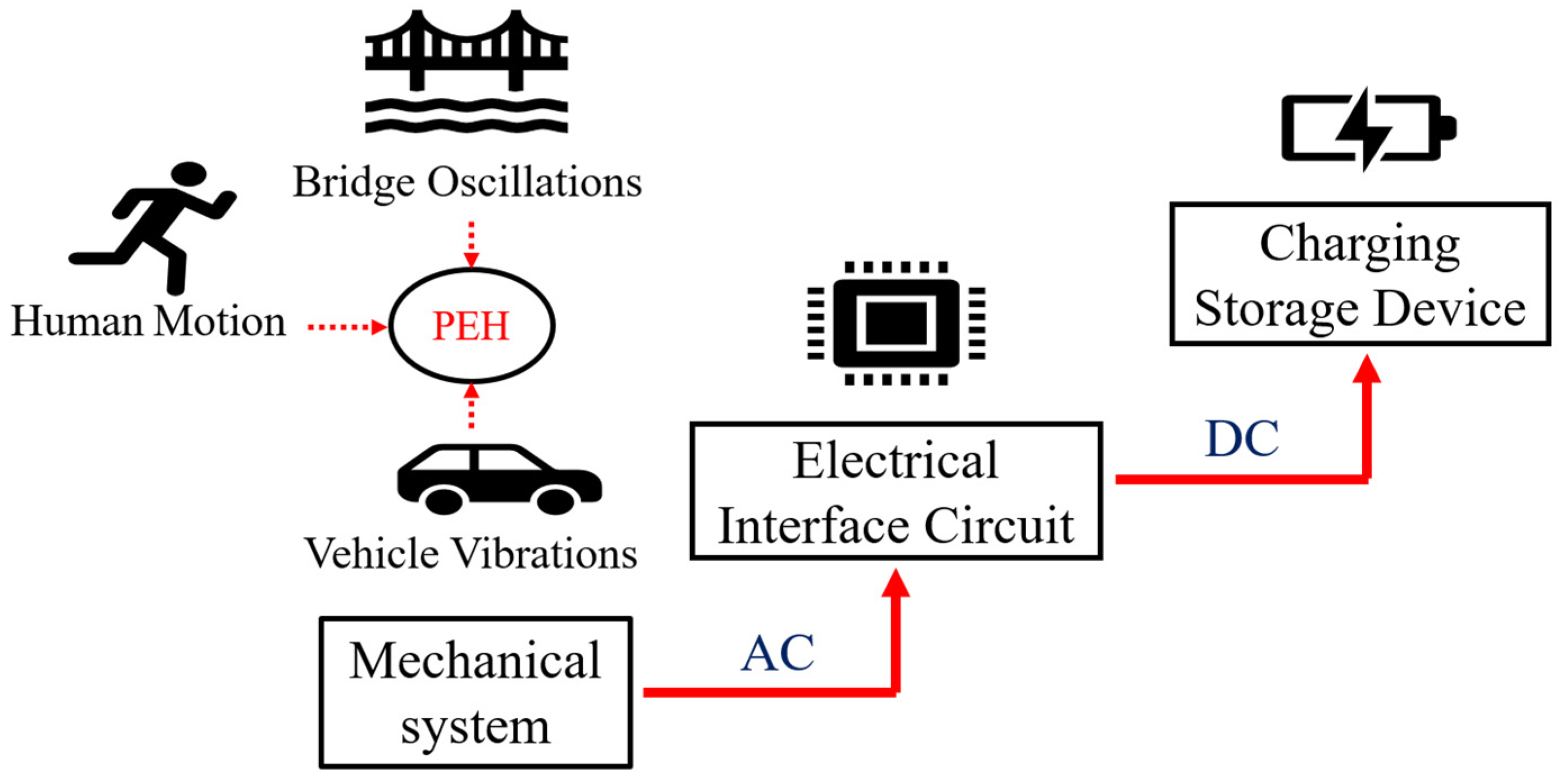
Figure 1. A conventional piezoelectric energy harvesting system.
Energies 16 02490 g001
Figure 2. (a) Piezoelectric device as a current source and, (b) The voltage and current output of the piezoelectric device.
Energies 16 02490 g002
Figure 3. (a) A voltage doubler circuit and, (b) The associated current and voltage waveforms.
Energies 16 02490 g003
Figure 4. (a) Proposed dual-stage boost converter circuit, (b) When the MOSFET switch (M1) is ON, (c) When the MOSFET switch (M1) is OFF.
Energies 16 02490 g004
Figure 5. Simulation model of the dual-stage boost converter circuit.
Energies 16 02490 g005
Figure 6. Ideal ac voltage source.
Energies 16 02490 g006
Figure 7. ON and OFF period of the MOSFET switch (M1).
Energies 16 02490 g007
Figure 8. Energising and De-energising process of the inductor (L1).
Energies 16 02490 g008
Figure 9. Charging and discharging process of the load capacitor (CL).
Energies 16 02490 g009
Figure 10. Experimental setup of the proposed circuit.
Energies 16 02490 g010
Figure 11. Outcomes of Test 1 at 3 Vac: (a) Output voltage (Vdc) and (b) Output power.
Energies 16 02490 g011
Figure 12. Outcomes of Test 1 at various excitation frequencies: (a) Output voltage (Vdc) and (b) Output power.
Energies 16 02490 g012
Figure 13. Outcomes of Test 2 at 1 Hz: (a) Output voltage (Vdc) and (b) Output power.
Energies 16 02490 g013
Figure 14. Outcomes of Test 2 at various excitation frequencies: (a) Output voltage (Vdc) and (b) Output power.
Energies 16 02490 g014
Table 1. Working intervals of a piezoelectric device and voltage doubler.
Electronic CircuitsMode 1: Positive Half-CycleMode 2: Negative Half-Cycle
Interval 1Interval 2Interval 3Interval 4
Piezoelectric deviceWhen to < t ≤ t1
  • CP: Charging
  • CL: Not charging
When t1 < t ≤ t2
  • CP: Discharging
  • CL: Charging
When t2 < t ≤ t3
  • CP: Charging
  • CL: Not charging
When t3 < t ≤ t4
  • CP: Discharging
  • CL: Charging
Voltage doublerWhen to < t ≤ t1
  • CP: Charging
  • D1: OFF
  • D2: OFF
  • CL: Not charging
When t1 < t ≤ t2
  • CP: Discharging
  • D1: ON
  • D2: OFF
  • CL: Charging
When t2 < t ≤ t3
  • CP: Charging
  • D1: OFF
  • D2: OFF
  • CL: Not charging
When t3 < t ≤ t4
  • CP: Discharging
  • D1: OFF
  • D2: ON
  • CL: Charging
Table 2. Working modes of Stage II.
Dual-Stage Boost Converter CircuitMode 3Mode 4
Stage IIM1: ON
L1: Charging
D4: OFF
CL: Discharging
M1: OFF
L1: Discharging
D4: ON
CL: Charging
Table 3. Components Table.
PartDescription
TypeReference
VacVoltage source5 V, 50 Hz
R1Resistor75 KΩ
R2Resistor200 Ω
RLLoad Resistor100 Ω
C1–C2Capacitor2.2 uF
C3Capacitor330 pF
CLLoad Capacitor500 uF
D1–D4 Schottky diode1N5819
M1N-MOSFETBSZ0920NS
Q1NPN-Transistor2N3904
L1Inductor4.7 uH
Table 4. Testing Sources.
Sources of ExcitationTest ScenariosFrequency
(Hz)
Input Voltage
(Vac)
Type of Piezoelectric DeviceLoad Resistors (KΩ)
Mechanical ShakerTest 11, 2, 3, 4, 5
10, 20, 30, 40, 50
5
3
MFCR1 = 100
R2 = 300
R3 = 620
R4 = 910
Test 21, 21, 2, 3, 4, 5
Table 5. Comparison of outputs of the circuits available in the previously published literature.
Circuit
Sources
No. of Piezoelectric DevicesInput Voltage (Vac)DC Voltage (Vdc)Output Power
(µ/mW)
External Power Supply
[35]11.2-30 µWYES
[36]320-33 µWYES
[15]15-22 µWNO
[27]33.5-254 µWYES
Proposed circuit13193.61 mWNO
Disclaimer/Publisher’s Note: The statements, opinions and data contained in all publications are solely those of the individual author(s) and contributor(s) and not of MDPI and/or the editor(s). MDPI and/or the editor(s) disclaim responsibility for any injury to people or property resulting from any ideas, methods, instructions or products referred to in the content.