Abstract
Traditional thermal sterilization technology is easy to implement and safe, but it will destroy food nutrition and change food taste. Therefore, people began to turn their attention to non-thermal sterilization. High-voltage pulsed electric field sterilization technology is one of them; it has attracted much attention because of its high efficiency and little damage to food. Different types of loads will cause serious trailing of the pulse falling edge. In view of this situation, this paper proposes a new topology circuit that combines a solid-state switch with a half-bridge Marx generator. It can be used for high-voltage pulsed electric field sterilization. By improving the structure of the classical Marx circuit, the high-voltage pulse power supply of the new topology circuit has the characteristics of steep rising edge and short falling edge delay; does not require isolation inductance or isolation resistance, which solves the isolation problem between the DC charging power supply and the high-voltage terminal; and has a good voltage-clamping function and load adaptability. The working process of the topology circuit under resistive, capacitive and inductive loads and the voltage clamping effect when the solid-state switch does not work properly in the discharge process are analyzed in detail. The power supply is composed of an adjustable DC power supply, five-stage half-bridge Marx generator and control protection circuit. A field programmable gate array (FPGA) is used as the controller to generate control signals, and optical fiber isolation is used to provide control signals for the main loop. The power supply can output a high-voltage square wave pulse with a voltage amplitude of 10 kV, maximum pulse number of 1000 per second, maximum pulse width of 20 μs, pulse rise time of smaller than 300 ns and short pulse drop time, and the repeated voltage amplitude, frequency and pulse width are adjustable, which can meet the requirements of a high-voltage pulse sterilization experiment.
1. Introduction
The energy utilization rate of thermal sterilization technology is low, and it will destroy the protein, enzyme, vitamin and other components in food, thereby damaging food nutrition and changing the natural flavor of food. With the improvement of people’s material living standards, people have higher requirements for the flavor of food on the basis of nutrition and health. Therefore, non-thermal sterilization technology has been developed, such as applying preservatives, light radiation, refrigeration and other physical methods, which relatively reduce the waste of energy, but also keep relatively more of the taste of food [1,2,3]. In the non-thermal sterilization technology, the high-voltage pulsed electric field sterilization technology has great market value, and it has been widely concerned due to its advantages of small temperature rise, high efficiency and short sterilization time [4,5].
The Marx generator has been gradually applied in high-voltage pulsed electric field sterilization due to its simple structure, low requirement for input power and high voltage obtained through a multi-stage series connection. In recent years, the spark switch has been replaced by a power semiconductor solid-state switch and the resistance has been replaced by a diode in the classical Marx circuit, which greatly improves the working performance of the pulse source [6,7]. However, the isolation problem between the DC charging power supply and the high-voltage side of the classical Marx generator still exists: when using resistance isolation, the charging current of the capacitor will be limited, which limits the power, output voltage, frequency and other parameters of the pulse source [8]. When inductance isolation is used, the output pulse width and insulation problems need to be considered, and its design is difficult. When the classical Marx generator drives the capacitive load, the charge on the load cannot be released immediately after the discharge of the pulse power supply, and the capacitive voltage of the load cannot decrease rapidly. This phenomenon has brought many adverse effects, which have a great influence on the waveform and make it difficult to obtain the square wave [9].
Ref. [10] shows that a pulsed electric field sterilization power supply is developed by using IGBT series technology to form high-voltage and large-capacity solid-state switches. The power supply has a simple structure, but it requires a high DC voltage, the output pulse width is difficult to control accurately, the load adaptability is poor and it is difficult to drive capacitive or inductive load. Ref. [11] shows that a high-power high-voltage pulsed electric field sterilization power supply combined with a classical Marx generator and IGBT was developed, which separates the DC charging power supply from the high-voltage terminal with inductance isolation. When the output pulse width and load are fixed, the power supply has good performance. When the output pulse width increases, the discharge time increases, and the isolation ability decreases with the increase in the current of the isolation inductor. The charging power supply and IGBT are easy to overcurrent, resulting in the burning of the system. Moreover, the boost effect caused by inductance isolation makes the energy storage capacitor voltage exceed the charging power supply voltage, and the output voltage becomes unstable and difficult to control accurately.
The main factors affecting the sterilization effect of high-voltage pulsed electric fields are as follows: pulsed electric field intensity, pulse action time, pulse waveform, pulse rise time and microbial characteristics [12].
(1) Pulsed electric field intensity. Studies have shown that the electric field intensity has the greatest impact on the sterilization effect. Only when the electric field intensity exceeds a certain critical value can the pulsed electric field have obvious sterilization effects. The microbial mortality caused by the transmembrane breakdown of the cell membrane was positively correlated with the pulsed electric field intensity. Most studies carried out sterilization experiments in an electric field intensity range of 1–4.5 kV/mm [13,14,15].
(2) Pulse action time. The pulse action time is a comprehensive reaction of the pulse width, pulse frequency, liquid flow rate and processing time. In a certain range, the longer the pulse time, the better the sterilization effect is. However, a longer pulse time will lead to a temperature rise, which will not only lead to a decrease in the energy efficiency, but also affect the sterilization effect. Generally, the pulse width is less than 20 µs.
(3) Pulse waveform. The pulse waveform is divided into square wave, exponential attenuation wave and oscillating attenuation wave. Among them, the square wave has the best sterilization effect, and the oscillating attenuation wave has the worst sterilization effect [16,17].
(4) Pulse rise time. In the cell transmembrane breakdown theory, the pulse rise time will affect the transmembrane potential. A steep rise edge has a better bactericidal effect on Staphylococcus aureus, and the temperature rise is smaller [18].
(5) Characteristics of microorganisms. Different types of microorganisms have different cell structures and sizes, as well as their ability to withstand high-voltage pulses and electrical characteristics. When the high-voltage pulse directly discharges the liquid containing bacteria and algae, its load characteristics are difficult to determine, which may show resistance, sensibility or capacitance [19].
As a key part of a pulsed electric field sterilization system, the performance of pulsed power directly affects the sterilization effect. Only when the electric field intensity reaches a certain degree can the sterilization effect be better, which requires a pulse power with high output. In the process of sterilization, the processing room and liquid food are used as the load of the pulse power supply. Due to the high conductivity of the processing room and liquid food, the resistance value is small, and the pulse power supply outputs a large current, so a high-power and high-voltage pulse power supply is needed. In addition, the structure of the treatment chamber and the types of microorganisms show different load characteristics, which may be resistive, capacitive and even inductive. At present, the output waveform of the high-power high-voltage pulse power supply used in the laboratory is mostly an exponential attenuation wave. Even a high-power high-voltage pulse power supply with a square wave output is difficult to rapidly decrease the pulse voltage under capacitive load, so that the normal output square wave cannot affect the sterilization effect.
In this paper, the classical Marx circuit is improved. Based on this, a high-power high-voltage pulse power supply that can output a square wave with rapid rising edge and short falling edge delay under various loads is proposed. It does not require isolation inductance or isolation resistance and has good function of the voltage clamp. Compared with some work, the circuit in this paper considers the problem of different properties of the load and shortens the tailing of the falling edge, which can reduce the abnormal discharge of liquid food. It can output a high-voltage square wave pulse with a voltage amplitude of 10 kV, maximum pulse number of 1000 per second, maximum pulse width of 20 μs, pulse rise time of smaller than 300 ns and short pulse drop time and its repeated voltage amplitude, frequency and pulse width are adjustable, which can meet the requirements of a high-voltage pulse sterilization experiment.
2. Working Process and Characteristic Analysis of New High-Voltage Pulse Power Supply
2.1. Topology Structure and Working Process of Circuit
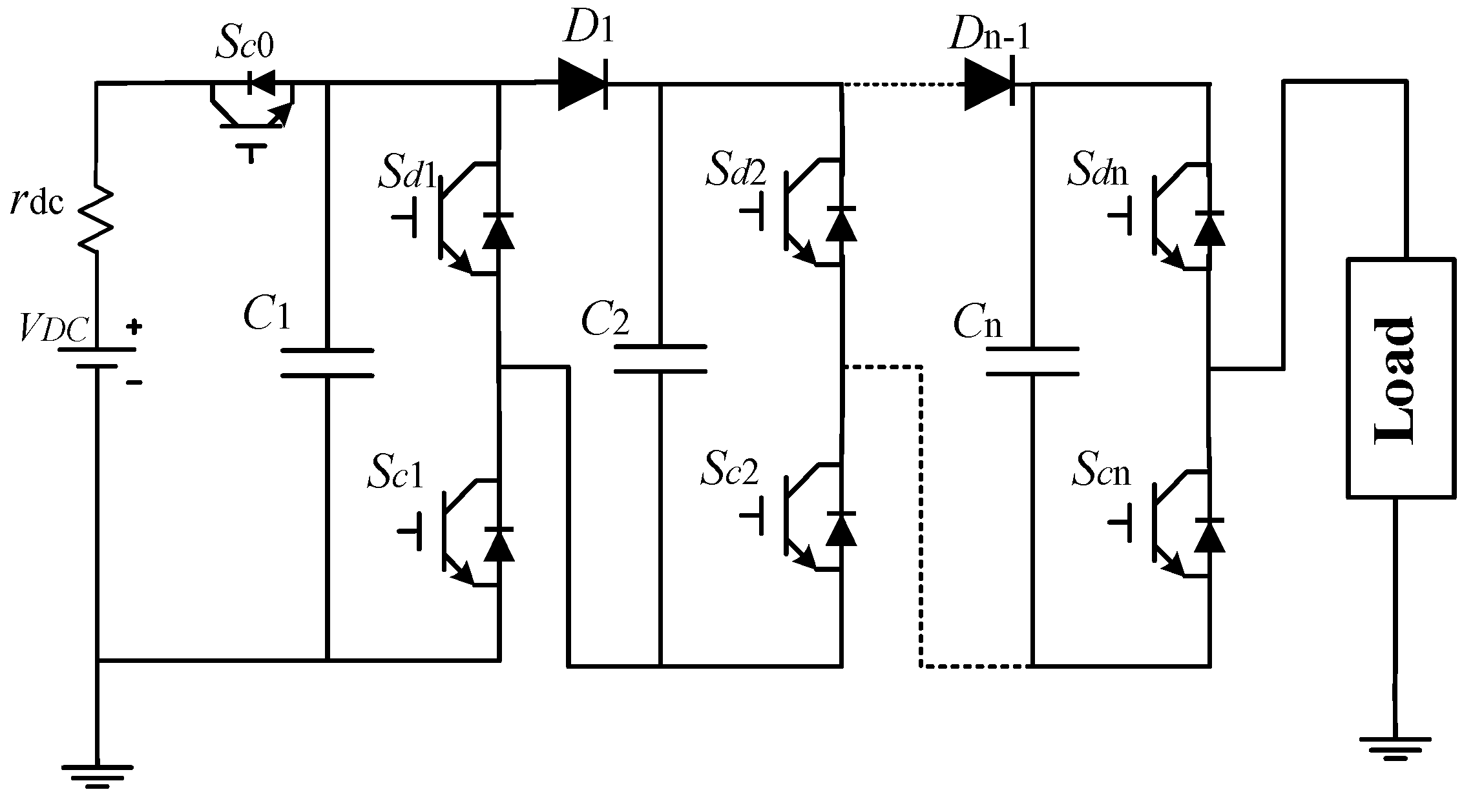
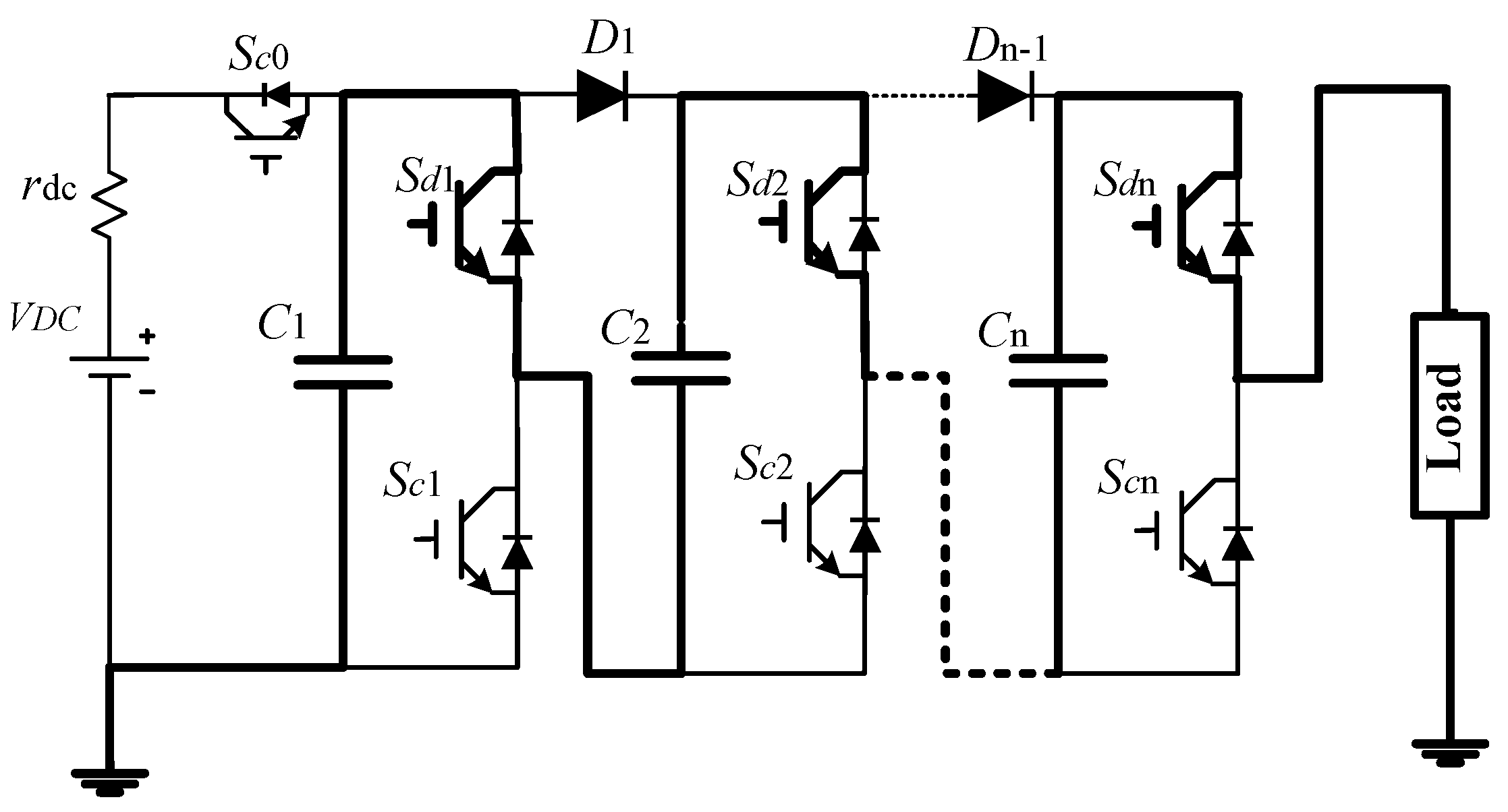
The Marx generator was first proposed by German scholar Erwin Otto Marx in 1923. Its working principle is summarized as parallel charging and series discharging. It realizes a high voltage output using capacitor voltage non-mutation and a switch device to realize step-by-step voltage superposition [20]. In this paper, a half-bridge Marx circuit is adopted to constitute the pulse source, which has the same working principle as the classic Marx and has been improved in structure. Its topological structure is shown in Figure 1.
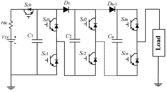
Figure 1.
Half−bridge Marx topological circuit.
In a half-bridge Marx circuit, each stage contains an energy storage capacitor Cn, two fully controlled semiconductor switches Sdn and Scn and a diode Dn. The circuit has two processes of discharge and charge, among which switches Sd1–Sdn control discharge and switches Sc1–Scn control charge and load short circuit.
The charging process is shown in Figure 2: When switches Sd1–Sdn are turned off and switches Sc0 and Sc1–Scn are turned on, the DC source VDC charges the storage capacitor C1–Cn through diodes D1–Dn−1 and switches Sc0 and Sc1–Scn. Meanwhile, the load is short-circuited by switches Sc1–Scn, the load releases the storage charge and the voltage drops rapidly.
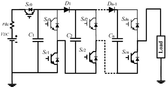
Figure 2.
Charging process of half–bridge Marx circuit.
The discharge process is shown in Figure 3: When the energy storage capacitors are full of electricity, switches Sc0 and Sc1–Scn are turned off, switches Sd1–Sdn are turned on and the energy storage capacitors C1–Cn are series connected to discharge the load. When switches Sd1–Sdn’s conductions are inconsistent, the energy storage capacitor and diode are connected in series and parallel with IGBT, which has the function of voltage clamping.
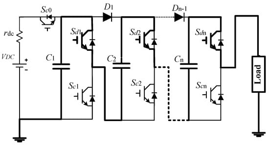
Figure 3.
Discharge process of half–bridge Marx circuit.
Compared to previous Marx circuits, the structure does not need isolation inductance or isolation resistance. When the pulse source outputs high-voltage pulses, switch Sc0 shuts off to isolate the DC charging power supply from the high-voltage pulse end, which solves the isolation problem between the DC charging power supply and the high-voltage end of the classical Marx circuit. Although the working process of it is similar to that of the classical Marx generator, its load is short-circuited off while charging, which makes it have the ability to drive resistance, inductive and capacitive loads.
2.2. Load Adaptability Analysis of High-Voltage Pulse Source
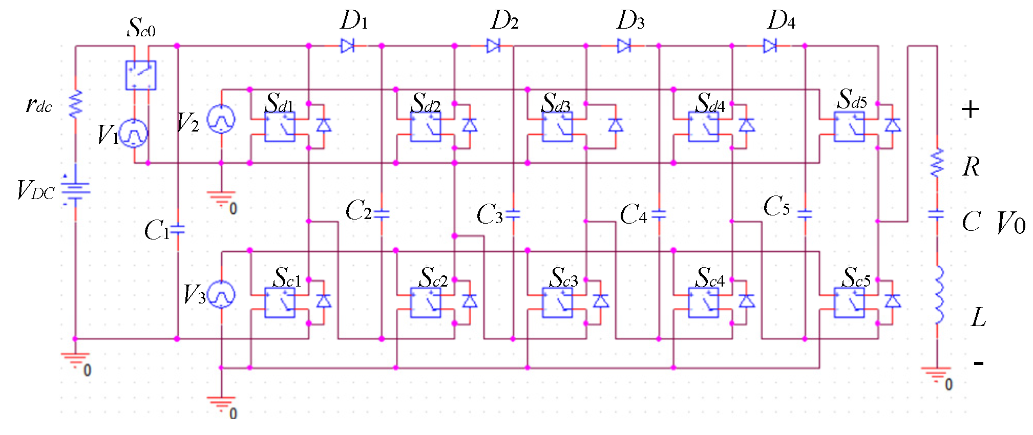
The characteristics of a half-bridge Marx circuit under resistive, inductive and capacitive loads are analyzed using simulations, and the parameters are shown in Table 1. As shown in Figure 4, the 5-stage half-bridge Marx circuit is simulated with OrCAD, in which each stage is composed of Cn, Sdn, Scn and Dn and the ideal voltage control switch is used to replace IGBT. Its input voltage VDC is 2000 V, rdc is 2 Ω and capacitance is 10 μF. In the circuit, signal V1 controls switch Sc0, V2 controls switches Sd1–Sd5 and V3 controls switches Sc1–Sc5.

Table 1.
Related parameters of output voltage of pulse power supply.
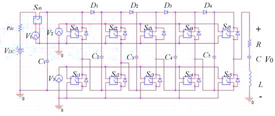
Figure 4.
Half−bridge Marx simulation schematic diagram.
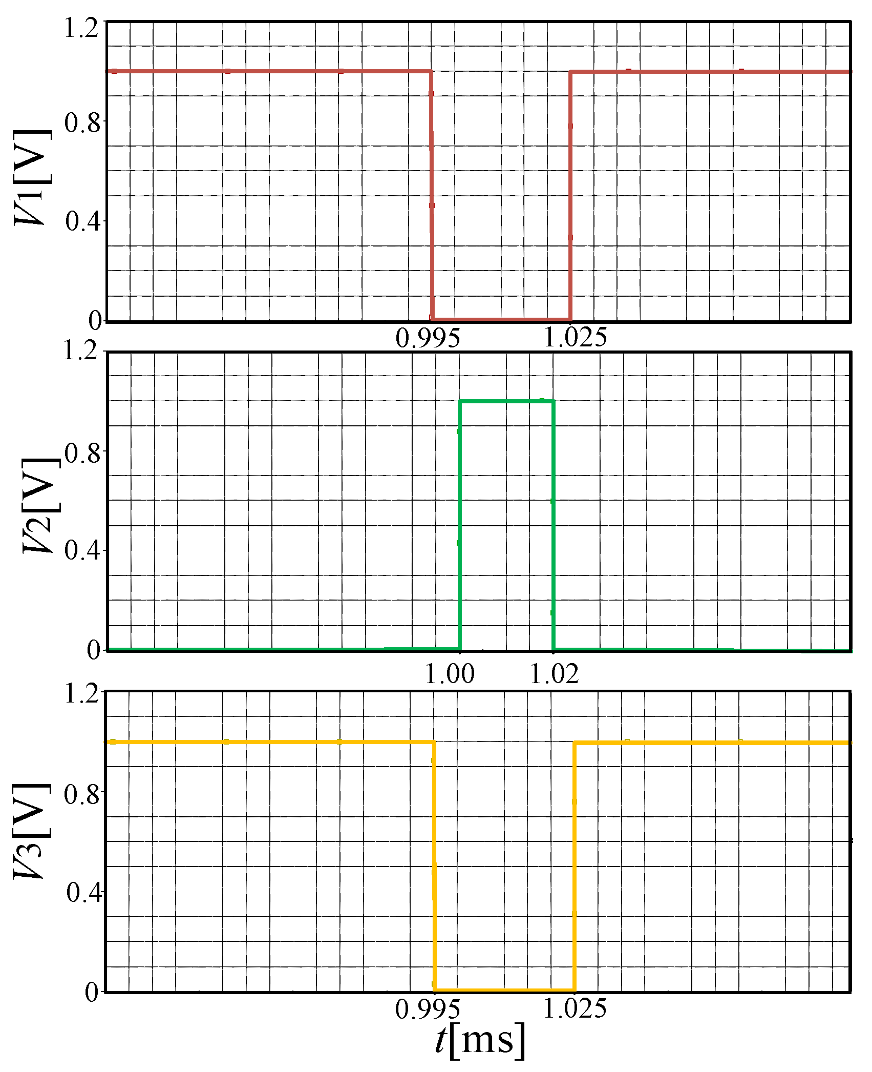
The control sequence of the switch is shown in Figure 5. The simulation is carried out under resistive, capacitive and inductive conditions to analyze the working process of the circuit under different loads.
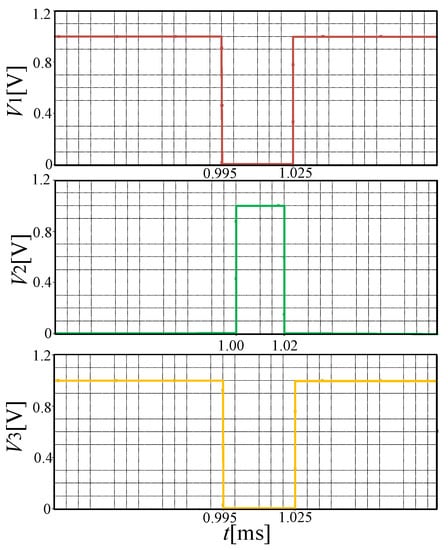
Figure 5.
Control sequence waveform diagram.
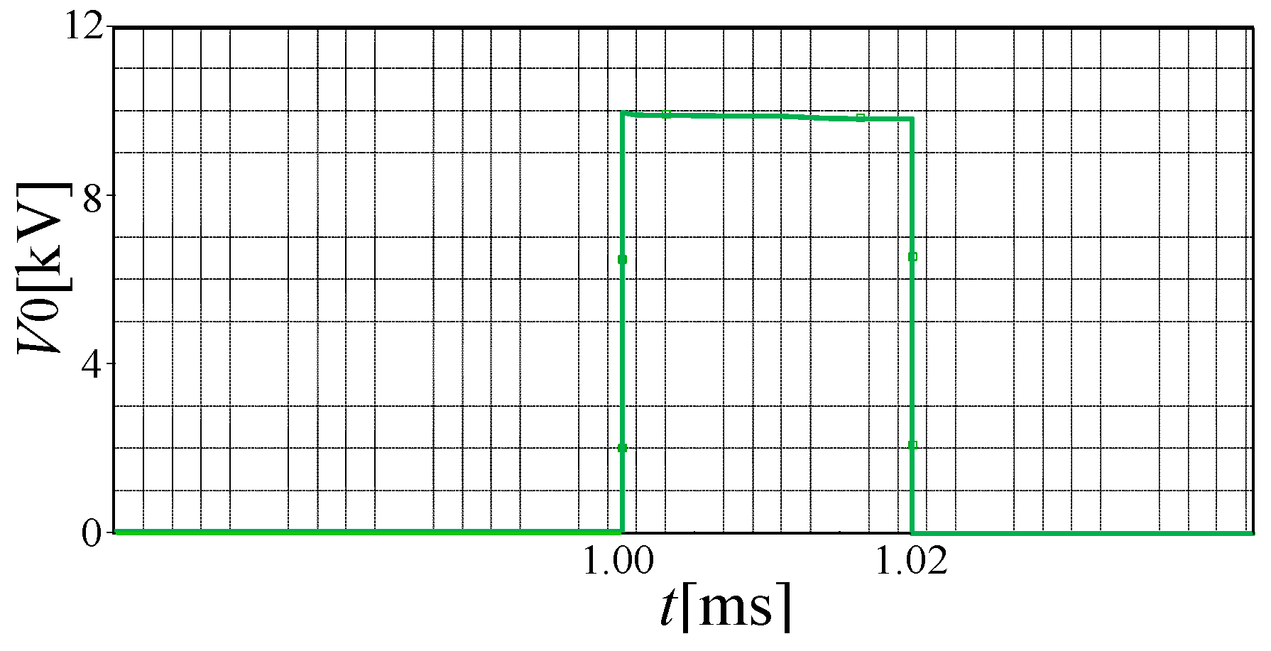
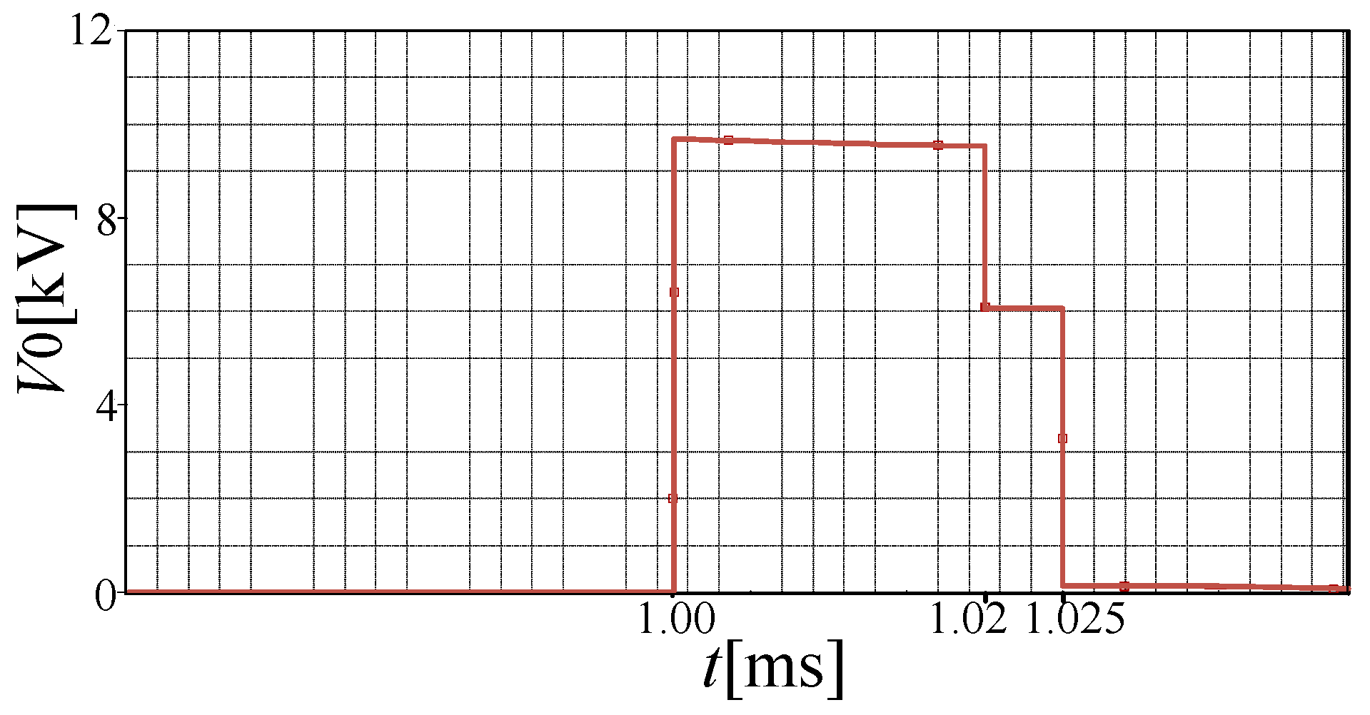
When R = 200 Ω, L = 0 and C = 0, the whole load can be regarded as a resistive load, and the pulse voltage waveform is shown in Figure 6. It will be analyzed below. At 0.9–0.995 ms, it is the charging time; switches Sc0 and Sc1–Sc5 are in the on state, Sd1–Sd5 are in the off state and the current output from VDC charges the energy storage capacitor through diodes and switches Sc0 and Sc1–Scn. At 0.995–1.0 ms, it is the dead-time waiting time. At this time, the circuit waits for Sc1–Sc5 to completely turn off and then turns on Sd1–Sd5 to prevent the same level of charging switch and discharge switch from turning on at the same time, resulting in a short circuit. At 1.0–1.02 ms, it is the discharging time; switch Sc0 is off to separate the DC charging power supply from the high-voltage pulse circuit, switches Sc1–Sc5 are off, switches Sd1–Sd5 are on and energy storage capacitors C1–C5 are connected in series and discharge to the load. From 1.02 to 1.025 ms is also the dead zone waiting time, the end of this cycle. It can be seen that the amplitude of the output pulse voltage is 10 kV, and there is a certain voltage top drop in the pulse waveform.
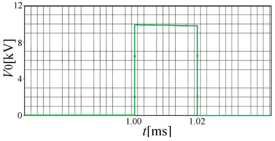
Figure 6.
Simulation waveform under resistive load.
When R = 200 Ω, L = 0 and C = 0.44 μF, the whole load can be regarded as a capacitive load. The pulse voltage waveform is shown in Figure 7, which is different from that under a resistive load. During 1.00–1.02 ms, its working process is the same as that under a resistive load, but the difference is that the top voltage drop under a capacitive load is small. At 1.02–1.025 ms, switches Sd1–Sd5 are in the off state, and switches Sc1–Sc5 are not turned on. Because of the capacitive load, the voltage will not drop to zero, but maintain a certain voltage, and if there is no discharge circuit, the voltage will remain. At 1.025 ms, switches Sc1–Sc5 turn off to turn on, the discharge circuit of the load capacitor starts to turn on and the voltage drops rapidly to 0.
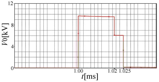
Figure 7.
Simulation waveform under capacitive load.
When R = 200 Ω, C = 0 and L = 20 mH, the load as a whole can be regarded as an inductive load. The pulse voltage waveform is shown in Figure 8, which is similar to that under a resistive load, but slightly different. In the discharge process of the Marx circuit, the load voltage changes rapidly, and the load current increases rapidly. Due to the existence of inductance, the pulse voltage has a certain degree of overshoot. At the end of the discharge, because the inductance current cannot change abruptly, the inductance forms a circuit by switching the anti-parallel diode of Sd1–Sd5, the current is rapidly reduced to 0 and the voltage on the load is also rapidly reduced to 0. Therefore, the time of the pulse drop edge under an inductive load is greater than that under a resistive load.

Figure 8.
Simulation waveform under inductive load.
By analyzing the working process under resistive, inductive and capacitive loads, it can be seen that the half-bridge Marx circuit can work normally under different loads, with a good output pulse voltage waveform and good load adaptability.
2.3. Voltage Clamp Analysis in Discharge Process
When IGBT does not conduct normally during discharge, the current flow path is shown in Figure 9.
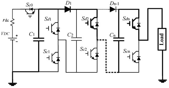
Figure 9.
Voltage−clamp process.
The first case: in the discharge process, except for Sd2, all Sd1–Sd5 changed from the off to the on state, and only Sd2 failed to on-state normally. The simulation results are shown in Figure 10. Compared with Sd1, it can be seen that there is no overvoltage on Sd2. The second case: in the discharge process, it is assumed that in Sd1–Sd5, except Sd2, all maintain the conduction state, and only Sd2 shuts down in advance. The voltage on Sd2 is shown in Figure 11 and Sd1 is selected for comparison; it can be seen that there is no overvoltage on Sd2.

Figure 10.
Voltage waveform when the switch is not normally on.
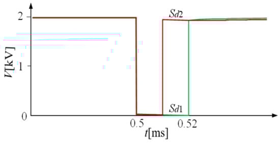
Figure 11.
Voltage waveform when the switch is turned off in advance.
Through the analysis of the abnormal working process of IGBT in the above two discharge processes, it can be seen that the half-bridge Marx circuit has a good voltage clamping effect.
3. Selection of Main Component Parameters of Pulse Power Supply
3.1. Selection of Capacitor
The selection of capacitor needs to consider the rated voltage and capacitance. When the capacitor is charged, the voltage of each capacitor is 2000 V. In practical application, the voltage margin should be kept; that is, the voltage value of the two ends of the capacitor is 60–70% of the voltage withstand value. In order to ensure the safety of the experiment, the voltage withstand value of the capacitor is 4 kV.
The selection of capacitance should consider the top voltage drop. When discharging at the maximum pulse width, the voltage value on the series capacitor cannot be reduced to the required minimum voltage value. In this paper, the minimum capacitance of a single capacitor is calculated by (1).
where n is the series of half-bridge Marx circuit, ΔUD is the maximum top voltage drop, tM is the maximum pulse width and Iroad is the average current flowing through the load. In summary, the main capacitor is composed of four nonpolar thin-film capacitors in parallel, whose voltage withstand value is 4 kV and capacitance is 2.5 μF.
3.2. Selection of Diode
The selection of diode needs to consider the maximum reverse operating voltage and the maximum forward average current. Since the charging voltage in the loop is 2 kV, the maximum reverse operating voltage should be greater than 2 kV. The maximum forward average current of the diode should be considered not only in the normal working state but also in the abnormal working state.
In the discharge process, when Sd1 is not normally on, due to the clamping effect of the circuit, the energy storage capacitor will be connected in series with the diode D1 to discharge to the load. At this time, the rated current of the diode must be considered. According to the parameters proposed for the power supply in this paper, the pulse voltage amplitude is 10 kV, and the impedance of the load is between tens of ohms and hundreds of ohms, so the diode has to withstand tens of amperes or even hundreds of amperes of current. The parameters of diode ZK800 are shown in Table 2, which can meet the requirements.
Table 2.
Parameters of ZK800.
3.3. Selection of IGBT
The selection of IGBT is similar to the selection of diode, which needs to consider the rated voltage and current, in addition to its switching speed and loss. The FZ800R33KF2C module produced by Infineon is selected for IGBT. Its maximum breakdown voltage is 3300 V, its current flow is 800 A at 80 °C, its conducting time is 280 ns and its ramp time is 1550 ns.
4. Controlling and Driving Circuits
4.1. Driving Circuit
The driving circuit uses driver board TX-DF102 of Luomuyuan. Its maximum output power is 4.5 W and output current is 40 A, and it can drive the IGBT module FZ800R33KF2C. Its input signal is connected by an optical fiber, so the isolation voltage is high. It has a three-stage perfect overcurrent protection function and an overcurrent alarm function. In addition, the driver board can be directly embedded in the selected IGBT module FZ800R33KF2C, which can make the power supply more compact.
The photoelectric conversion board TX-JKDF1A is used in conjunction with the drive board TX-DF102. The electrical signal generated by FPGA is converted into an optical signal through the photoelectric conversion board, and the TX-DF102 driving board controls the conduction and shutdown of IGBT through the input optical signal.
4.2. Controlling Circuit
For the controlling circuit, we selected the FPGA hardware development platform AX301 as the controller, which has 68 I/O ports for users, contains a 50 MHz crystal oscillator circuit and can produce a good-stability, high-pulse-frequency precision pulse. It obtains the required control signal by dividing the global input clock.
In order to prevent the IGBT in the upper and lower arms from short circuiting at the same time, which leads to the burning of the system, the over-current protection circuit is added to the system. When the overcurrent flows through IGBT, the driver board TX-DF102 will output an alarm signal, which is fed back to the controller FPGA through the photoelectric conversion board to protect the circuit in real time.
5. Construction and Performance Test of Prototype
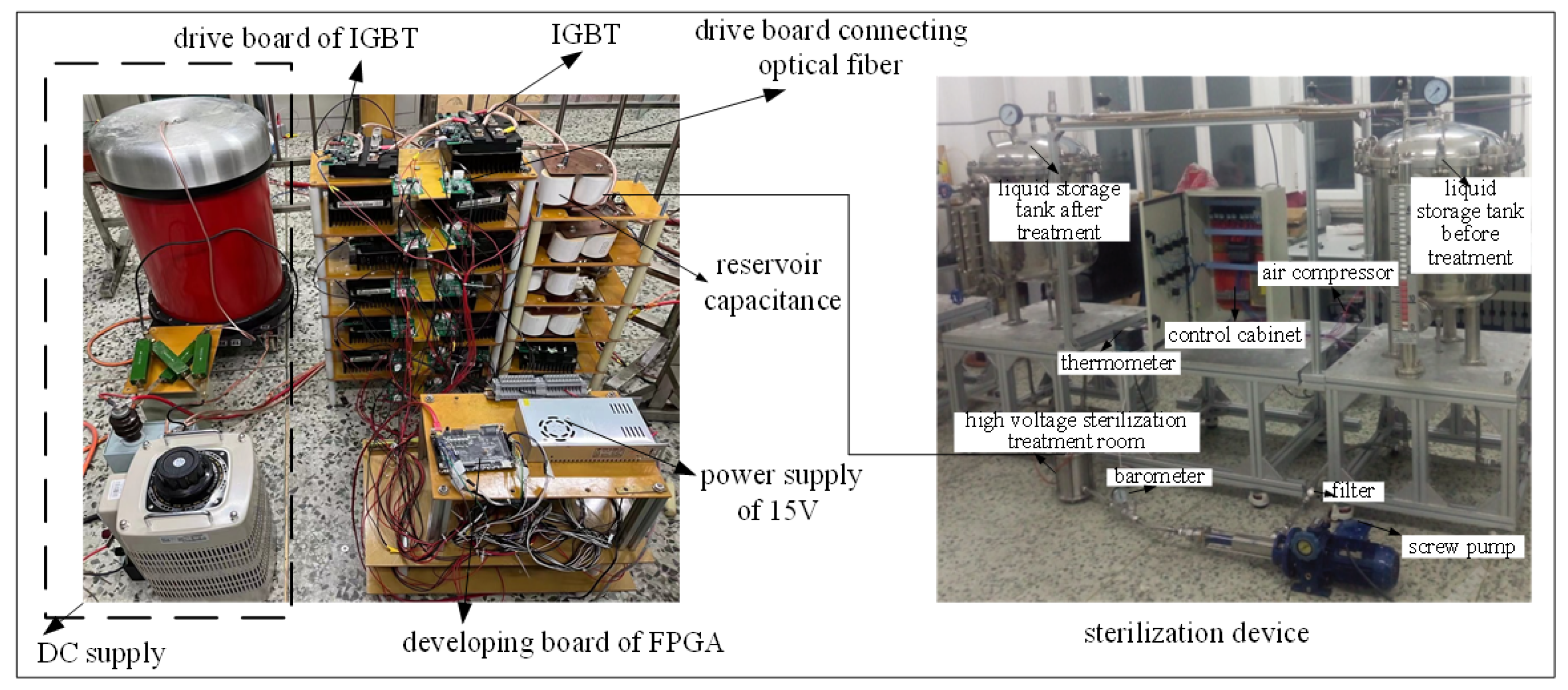
DC power is obtained through the regulator, transformer, high-voltage rectifier silicon stack and filter capacitor. According to the above design scheme and device selection, a high-voltage pulsed electric field sterilization power supply is built, as shown in Figure 12.
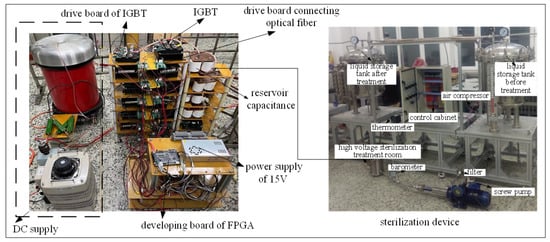
Figure 12.
Physical drawing of power supply.
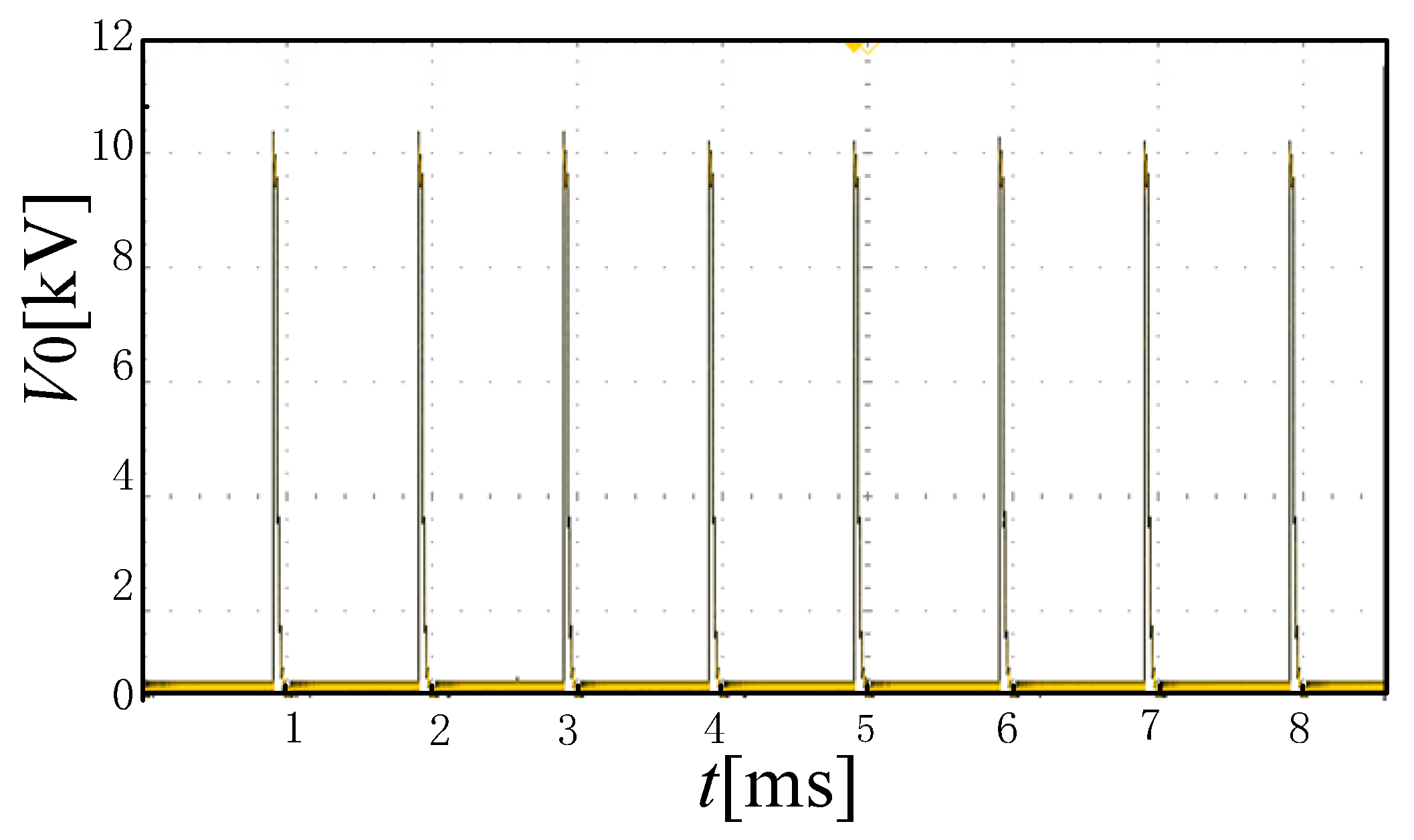
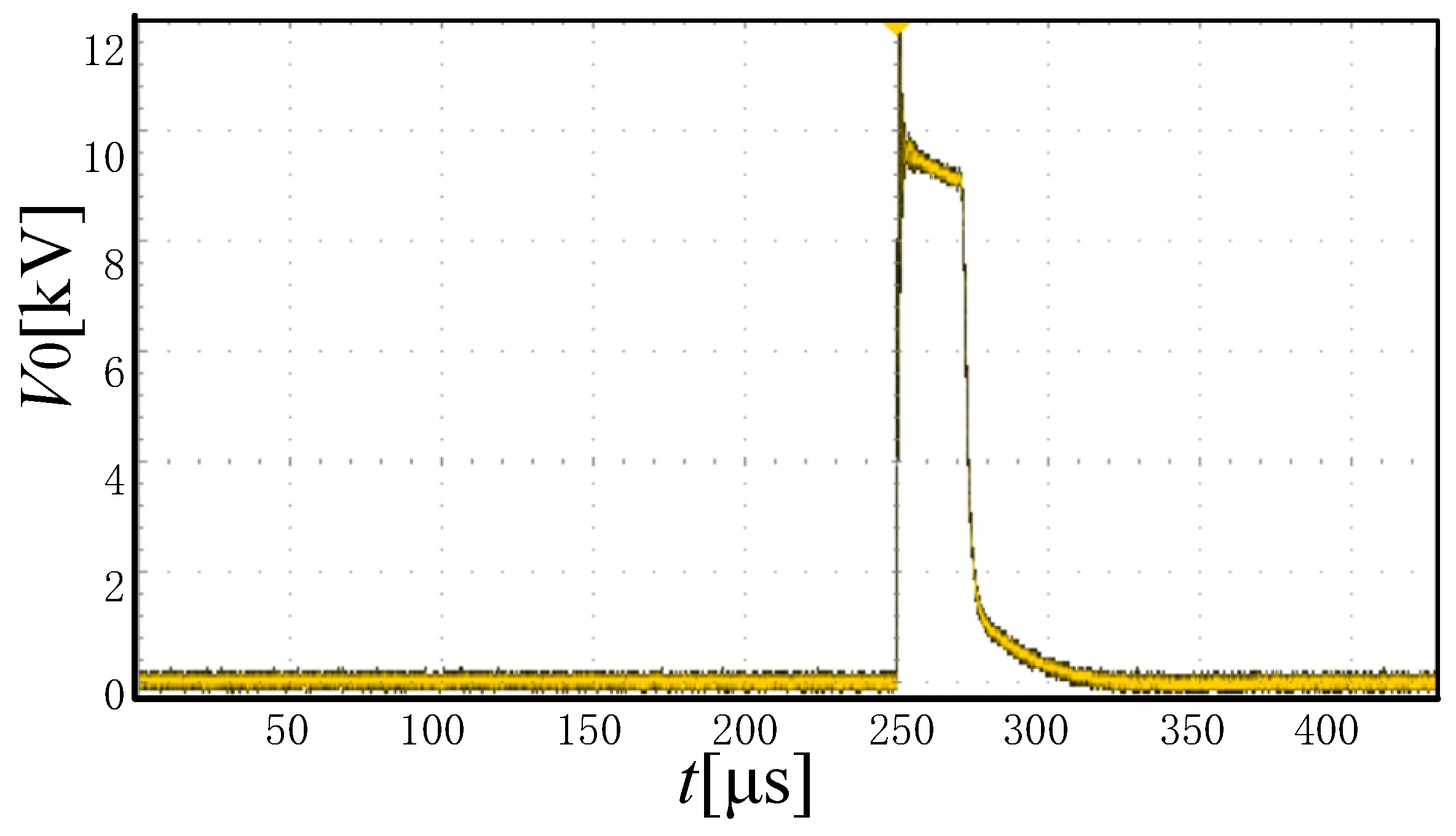
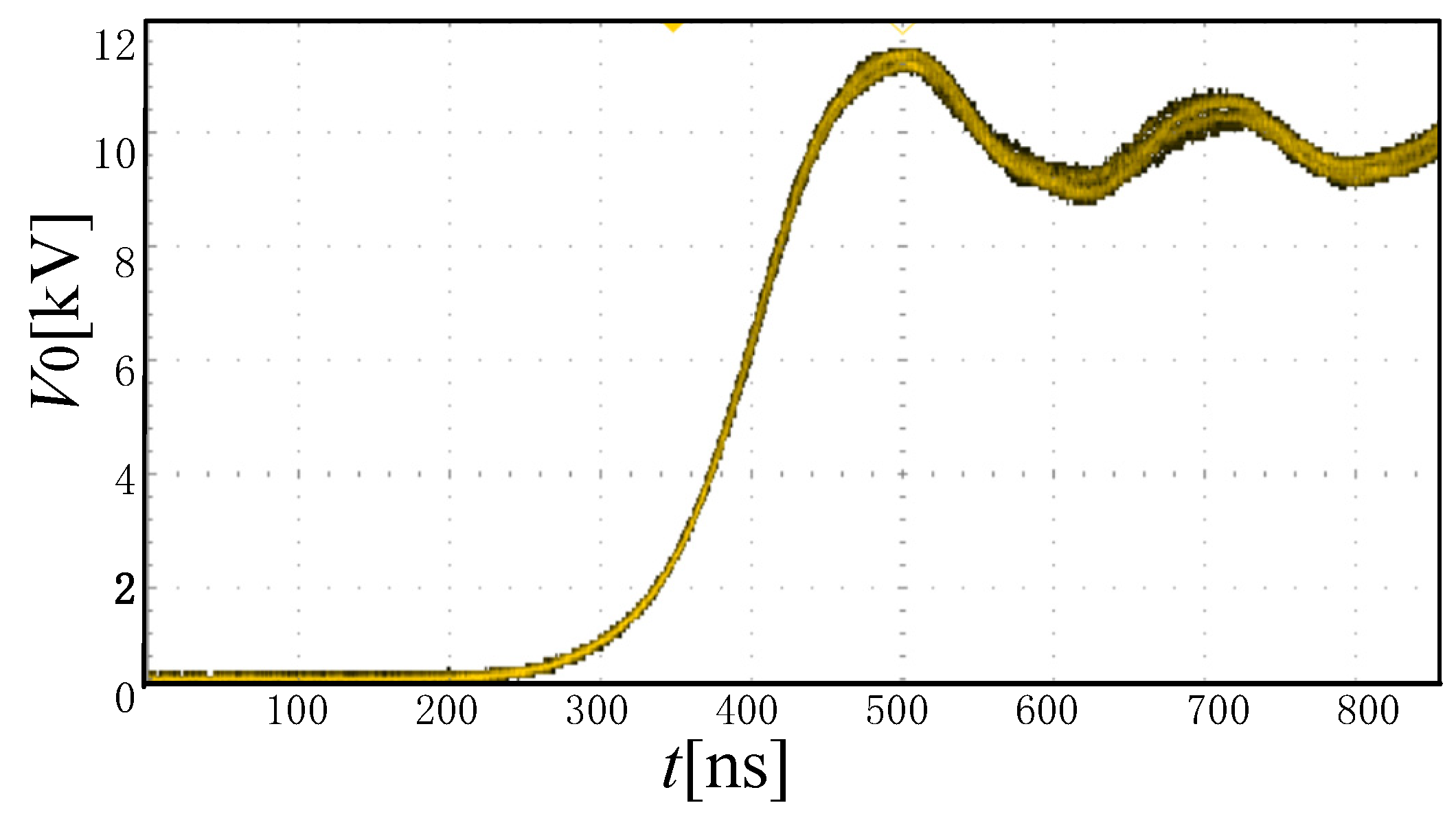
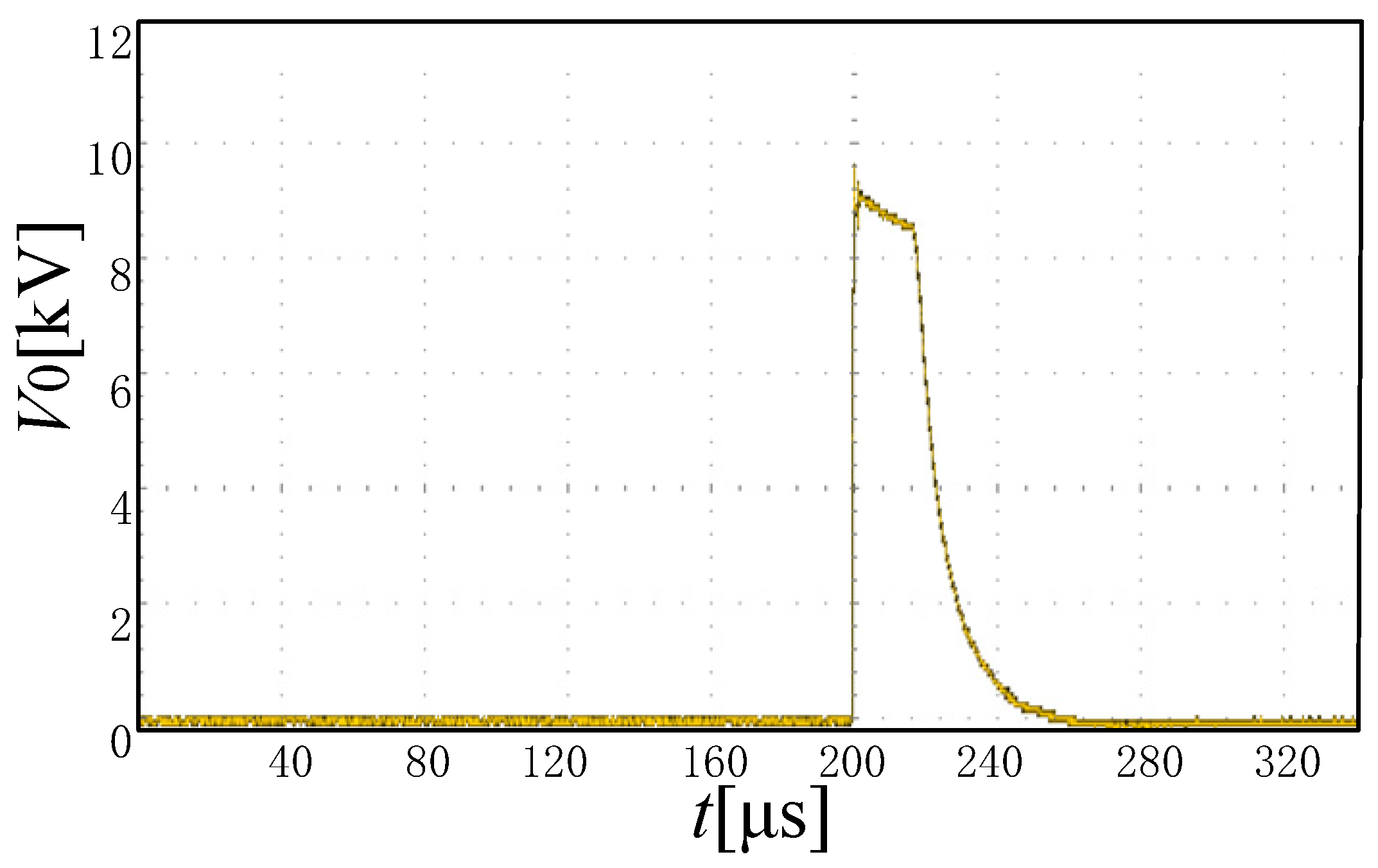
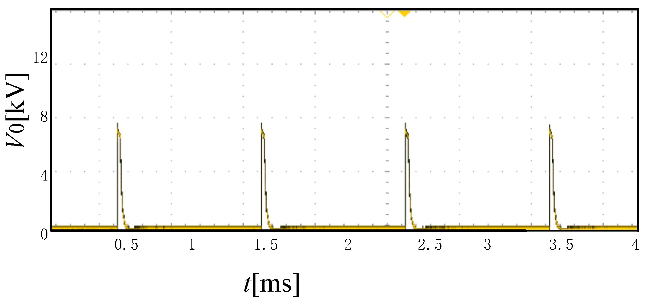
In the experiment, the voltage measurement uses the GWINSTEK GDS-3152 oscilloscope with a bandwidth of 150 MHz and a Tek P6015A high-voltage probe with a bandwidth of 75 MHz. The system output pulse number is 1000 pps, the pulse width is 20 μs and the DC power supply voltage is 2 kV. When the load is 200 Ω, the pulse waveform is as shown in Figure 13, the pulse voltage amplitude is 10 kV and the pulse frequency is 1000 pps. The pulse waveform is shown in Figure 14, and the output pulse width is 20 µs. The waveform of the pulse rising time is shown in Figure 15, indicating that the pulse rising time is less than 300 ns.
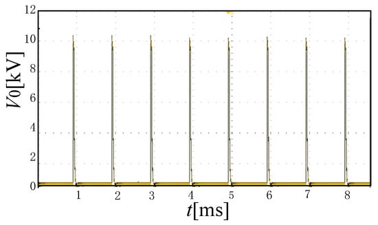
Figure 13.
Full view of pulse waveform under resistive load.

Figure 14.
Pulse pattern under resistive load.
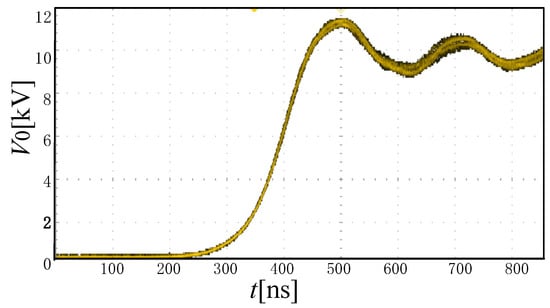
Figure 15.
Pulse rising edge waveform under resistive load.
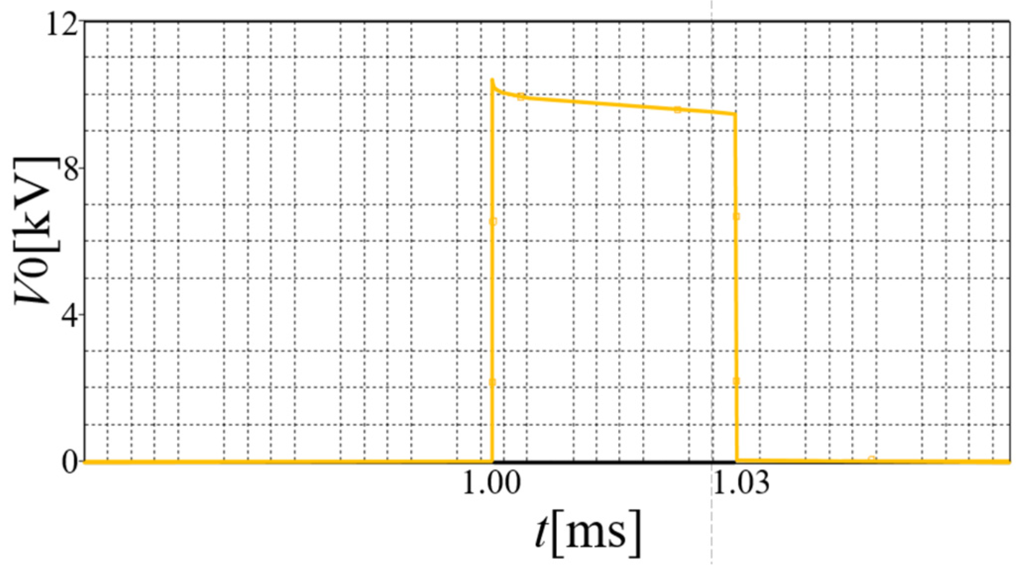
Comparing Figure 6 and Figure 14, the two are the output waveforms obtained using simulations and experiments, respectively, when the load is resistive. It can be seen that the pulse width in the simulation is 19 μs, and that measured in the experiment is about 20 μs, which leads us to consider that the experimental results are consistent with the simulation results within the allowable error range. Due to the influence of stray inductance in the experimental circuit, the measured waveform has some oscillation, rather than the same steady voltage as the simulation.
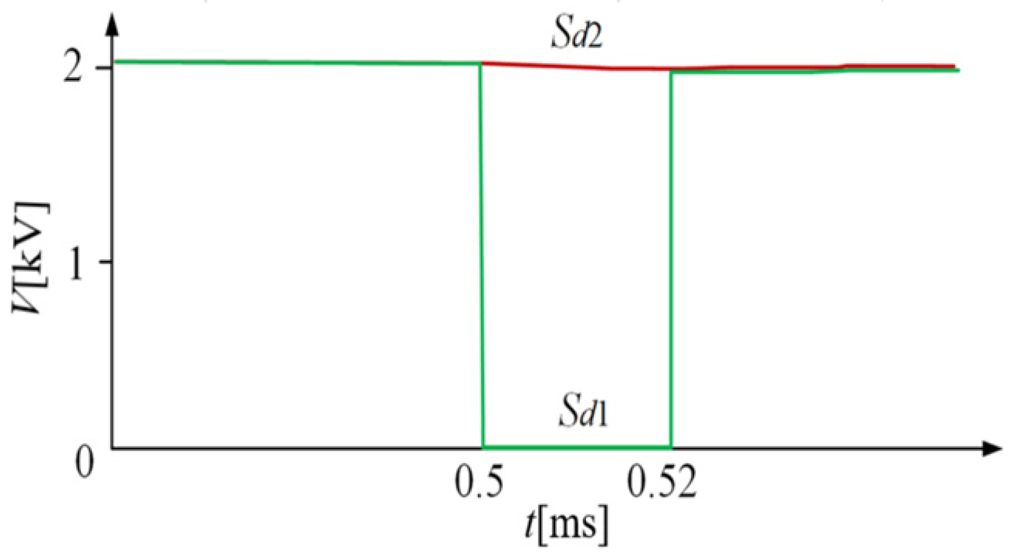
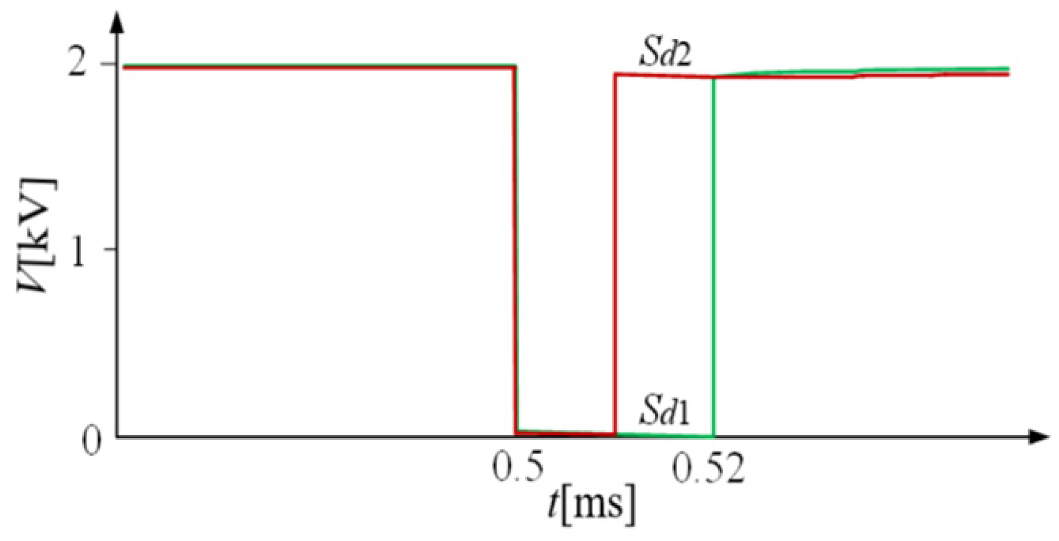
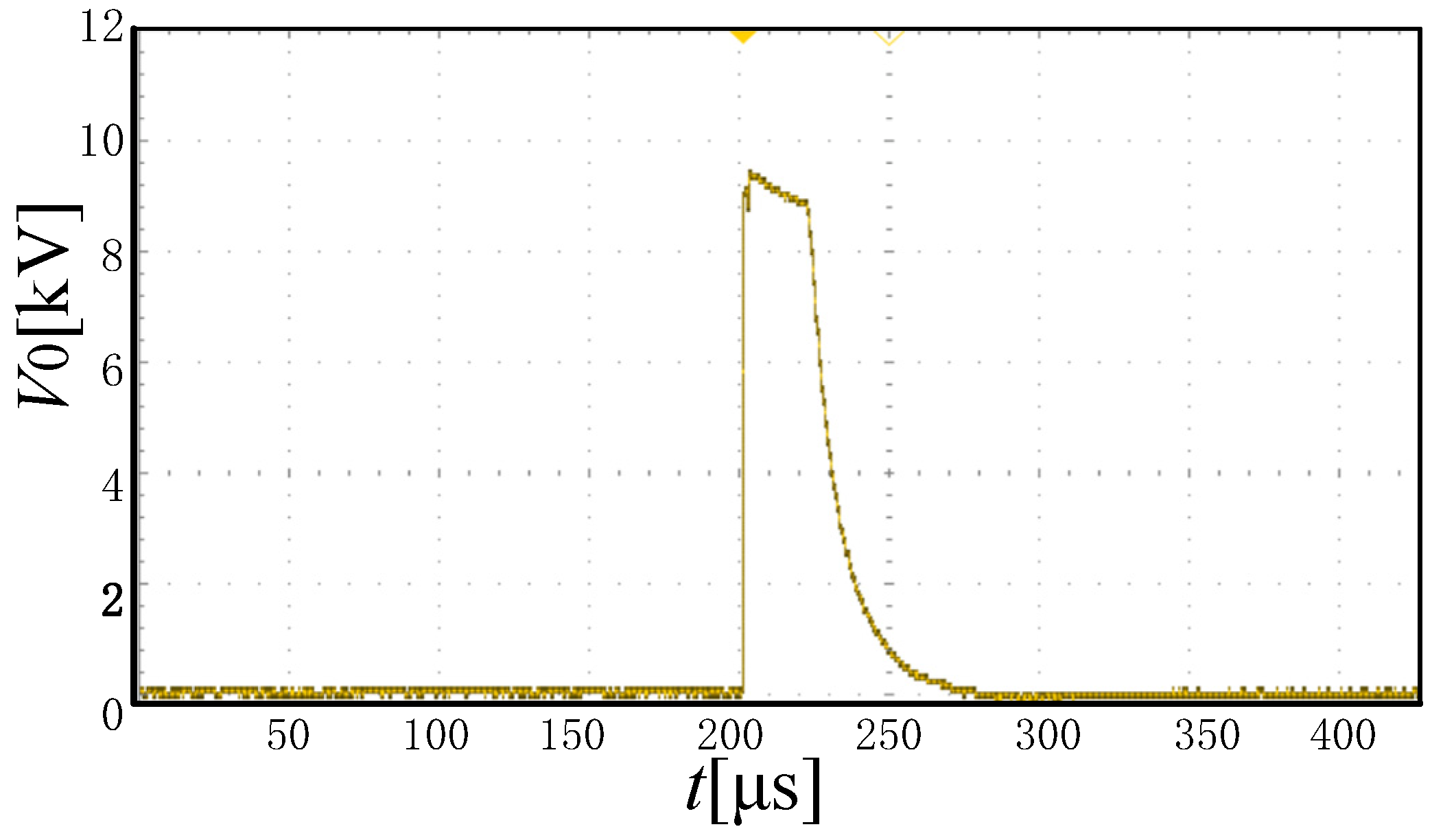
In order to verify the load adaptability of the power supply, the load is replaced by a capacitive load composed of a 200 Ω resistor and a 0.44 μF capacitor in series. The pulse waveform is shown in Figure 16, which has an obvious pulse trailing phenomenon compared with the pulse waveform under a resistive load. By changing the timing control schemes of IGBT, the load capacitor is discharged in time, and the output waveform is shown in Figure 17. It can be seen that the pulse decreases rapidly with obvious truncation.
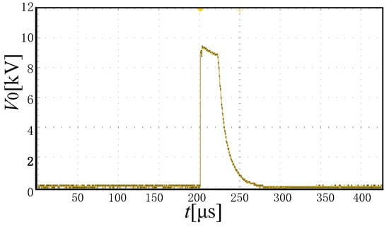
Figure 16.
Pulse pattern under capacitive load.

Figure 17.
Pulse truncated image.
Comparing Figure 7 with Figure 16, they are the simulated output waveform and the experimentally measured waveform, respectively, when the load is resistance and capacitance in series. It can be seen that the two waveforms are roughly the same within the allowable range of error. In the first 25 μs, due to the influence of the capacitor load, they are in the peak voltage state and discharge rapidly after the subsequent discharge circuit is connected, and the pulse falling edge is relatively small.
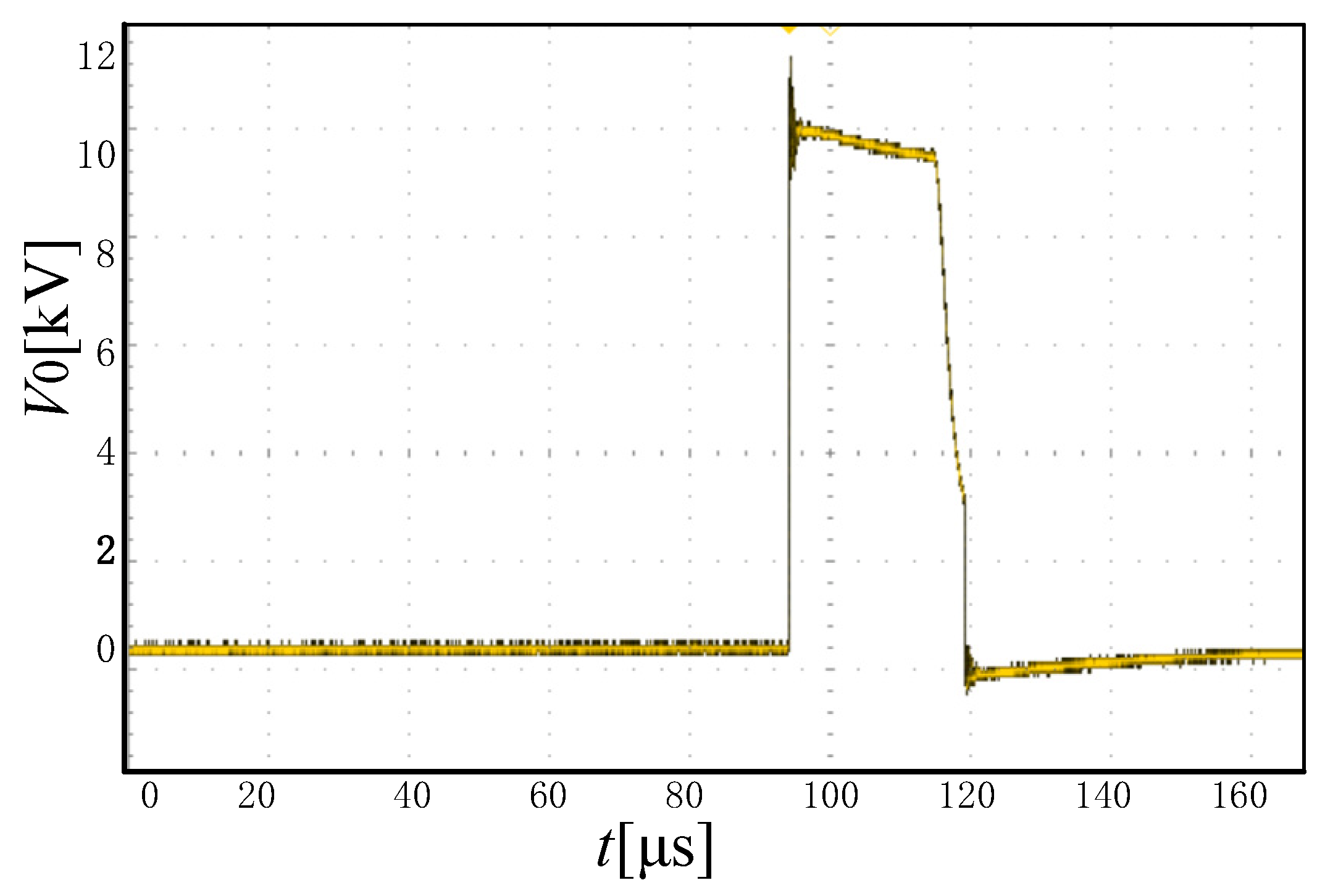
When the load is replaced by an inductive load consisting of 200 Ω resistance and 20 µH inductor in series, the output pulse waveform of the power supply is shown in Figure 18. It can be seen that the pulse decline time is longer than that under a resistive load.
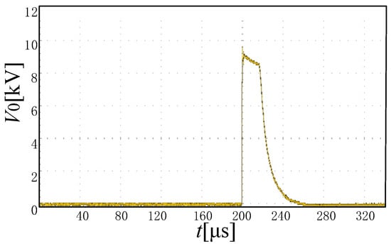
Figure 18.
Pulse waveform under inductive load.
Comparing Figure 8 with Figure 18, the two are the output waveforms obtained using simulations and experiments, respectively, when the load is resistance and inductance in series. Considering the actual situation, the voltage during the experiment does not fall vertically like the general voltage during the simulation. The simulation results show that the peak voltage time is extended to 30 μs, while the actual experimental results show that the pulse falling edge is extended. Both of them show the inhibition of inductance on current flow, but they are not exactly the same.
In the discharge process, one of the IGBTs is not turned on by changing the program, which simulates the process of IGBT not being turned on normally. As shown in Figure 19, the output voltage changes from 10 kV to 8 kV, and the voltage amplitude is the voltage of an energy storage capacitor, which verifies that the power supply has a good voltage clamping function.
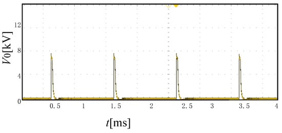
Figure 19.
Display of voltage clamping effect.
6. Conclusions
A pulse source for high-voltage pulsed electric field sterilization is designed. The pulse source uses IGBT as the main switch device. The power supply can output a high-voltage square wave pulse with a voltage amplitude of 10 kV, maximum pulse number of 1000 per second, pulse rise time of 300 ns and maximum pulse width of 20 μs, and the voltage amplitude, repetition frequency and pulse width are adjustable. The whole power supply uses FPGA as the controller to generate control signals, which are isolated by optical fiber, greatly improving the reliability of the system. The driving circuit has an IGBT overcurrent feedback function, which improves the safety of the system. The power supply has a good voltage clamping function and can drive resistive, point inductive and capacitive loads. The power supply does not need isolation resistance and isolation inductance, which shortens the charging time. Its shorter falling edge can reduce the generation of abnormal discharge of liquid food.
Author Contributions
Conceptualization, B.Z. and X.W.; Methodology, B.Z. and G.W.; Software, Z.F.; Validation, H.S., Z.F. and G.W.; Formal analysis, B.Z.; Investigation, H.S. and G.W.; Resources, B.Z. and X.W.; Writing – original draft, H.S. and Z.F.; Writing – review & editing, B.Z.; Supervision, B.Z. and X.W. All authors have read and agreed to the published version of the manuscript.
Funding
This research received no external funding.
Data Availability Statement
Not applicable.
Conflicts of Interest
The authors declare no conflict of interest.
References
- Takaki, K.; Hayashi, N.; Wang, D.; Ohshima, T. High-voltage technologies for agriculture and food processing. J. Phys. D Appl. Phys. 2019, 52, 3001. [Google Scholar] [CrossRef]
- Qin, B.; Zhang, Q.; Barbosa-Canovas, G.V.; Swanson, B.G.; Pedrow, P.D. Nonthermal pasteurization of liquid foods using high-intensity pulsed electric fields. Crit. Rev. Food Sci. Nutr. 1996, 36, 603–627. [Google Scholar] [CrossRef] [PubMed]
- Zhu, D.; Kebede, B.; Chen, G.; McComb, K.; Frew, R. Effects of the vat pasteurization process and refrigerated storage on the bovine milk metabolome. J. Dairy Sci. 2020, 103, 2077–2088. [Google Scholar] [CrossRef] [PubMed]
- Jayaram, S.H. Sterilization of liquid foods by pulsed electric fields. IEEE Electr. Insul. Mag. 2000, 16, 17–25. [Google Scholar] [CrossRef]
- Sevenich, R.; Kleinstueck, E.; Crews, C.; Anderson, W.; Pye, C.; Riddellova, K. High-pressure thermal sterilization: Food safety and food quality of baby food puree. J. Dairy Sci. 2014, 79, M230–M237. [Google Scholar] [CrossRef] [PubMed]
- Yao, C.; Zhang, X.; Guo, F.; Dong, S.; Mi, Y.; Sun, C. FPGA-Controlled All-Solid-State Nanosecond Pulse Generator for Biological Applications. IEEE Trans. Plasma Sci. 2012, 40, 2366–2372. [Google Scholar] [CrossRef]
- Sato, T.; Murakami, Y.; Muramoto, Y. Sterilization of escherichia coli by Marx circuit with switches using bipolar junction transistors. In Proceedings of the 2017 International Symposium on Electrical Insulating Materials (ISEIM), Toyohashi, Japan, 11–15 September 2017; pp. 199–202. [Google Scholar]
- Jin, Y.; Sun, W.; Yu, L.; He, D.; Dong, S.; Yao, C. A 10 kV Modular Solid Boost-Marx Pulse Generator with Inductive Isolation. In Proceedings of the 2022 IEEE International Conference on High Voltage Engineering and Applications (ICHVE), Chongqing, China, 25–29 September 2022; pp. 1–4. [Google Scholar]
- Abadi, M.Q.R.; Marzebali, M.H.; Abolghasemi, V.; Anisi, M.H. High-voltage pulse generators for electroporation applications: A systematic review. IEEE Access 2022, 10, 64933–64951. [Google Scholar] [CrossRef]
- Chen, X.; Yu, L.; Jiang, T.; Tian, H.; Huang, K.; Wang, J. A High-Voltage Solid-State Switch Based on Series Connection of IGBTs for PEF Applications. IEEE Trans. Plasma Sci. 2017, 45, 2328–2334. [Google Scholar] [CrossRef]
- Wei, X.; Wang, H.; Guo, Z. Development of industrial high voltage pulsed electric field sterilization power supply. Electr. Mach. Control 2019, 23, 65–72. [Google Scholar]
- Achour, Y.; Starzyński, J.; Jakubiuk, K. New Architecture of Solid-State High-Voltage Pulse Generators. Energies 2022, 15, 4823. [Google Scholar] [CrossRef]
- Chen, J.; Zhang, R.; Wang, L.; Mo, M. Effect of pulsed electric fields on proanthocyanidins in young red wine. In Proceedings of the 2009 IEEE 9th International Conference on the Properties and Applications of Dielectric Materials, Harbin, China, 19–23 July 2009; pp. 1124–1127. [Google Scholar]
- Zhang, R.; Cheng, L.; Wang, L.; Guan, Z. Inactivation Effects of PEF on Horseradish Peroxidase (HRP) and Pectinesterase (PE). IEEE Trans. Plasma Sci. 2006, 34, 2630–2636. [Google Scholar] [CrossRef]
- Chalise, P.R.; Perni, S.; Shama, G.; Novac, B.M.; Smith, I.R.; Kong, M.G. Interaction of Sub-Microsecond Pulsed Electric Field With Bacterial Cells. In Proceedings of the Conference Record of the 2006 Twenty-Seventh International Power Modulator Symposium, Arlington, VA, USA, 14–18 May 2006; pp. 562–565. [Google Scholar]
- Barsotti, L.; Merle, P.; Cheftel, J.C. Food processing by pulsed electric fields. I. Physical aspects. Food Rev. Int. 1999, 15, 163–180. [Google Scholar] [CrossRef]
- Qin, B.; Zhang, Q.; Barbosa-Canovas, G.V.; Swanson, B.G.; Pedrow, P.D. Inactivation of microorganisms by pulsed electric fields of different voltage waveforms. IEEE Trans. Dielectr. Electr. Insul. 1994, 1, 1047–1057. [Google Scholar]
- Chen, J.; Zhang, R.; Xiao, J.; Li, J.; Wang, L.; Guan, Z.; MacAlpine, M. Influence of Pulse Rise Time on the Inactivation of Staphylococcus Aureus by Pulsed Electric Fields. IEEE Trans. Plasma Sci. 2010, 38, 1935–1941. [Google Scholar] [CrossRef]
- Sun, B.; Aye, N.N.; Wang, X.; Zhu, X.; Sato, M. Eradication of Invasive Organisms From Ballast Water With Electrodeless Pulsed-Discharge Hybrid Reactor. IEEE Trans. Ind. Appl. 2011, 47, 1079–1085. [Google Scholar]
- Kholgh Khiz, A.; Banaei, M.R. Marx-based pulse generator with high-voltage gain. Int. J. Circuit Theory Appl. 2022, 50, 1101–1118. [Google Scholar] [CrossRef]


Disclaimer/Publisher’s Note: The statements, opinions and data contained in all publications are solely those of the individual author(s) and contributor(s) and not of MDPI and/or the editor(s). MDPI and/or the editor(s) disclaim responsibility for any injury to people or property resulting from any ideas, methods, instructions or products referred to in the content. |
© 2023 by the authors. Licensee MDPI, Basel, Switzerland. This article is an open access article distributed under the terms and conditions of the Creative Commons Attribution (CC BY) license (https://creativecommons.org/licenses/by/4.0/).