Abstract
There is always a need to analyze current signals generated by various DC–DC converters. For example, to determine the current stress experienced by semiconductor devices and to evaluate active and reactive power consumption in converters. The study demonstrates that the shape of a current signal dictates the analytical expressions required to determine the average and RMS values of a signal as well as the RMS value of the ripple of that signal. The study also shows that current signals can be treated as composite waveforms comprising various combinations of trapezoidal, rectangular, and triangular pulses. The current literature lacks a unified approach to analyze current stresses in DC–DC converters. This study will propose a unified and generalized analytical technique that is applicable to any type of DC waveform that can be treated as a composite waveform made up of a combination of triangular, rectangular, or trapezoidal sections or sub-intervals. Furthermore, the rectangular and triangular pulses are shown to be a special kind of trapezoidal pulse. This provides the basis for a very broad generalization of current signals’ analysis based on the analysis of a trapezoidal pulse. Additionally, a method for the direct evaluation of signals’ ripple RMS content is developed. This is unlike in the current literature where it is necessary to evaluate the signal’s average and RMS values before ripple content can be evaluated. The technique developed is applicable to continuous and discontinuous conduction modes of operation.
1. Introduction
The number and diversity of DC loads that include DC–AC converters, IT loads, electronic lighting, and electric vehicles continue to grow rapidly [1,2,3,4] in distribution networks. Similarly, the number of DC sources in the form of solar PV arrays, battery energy storage systems, fuel cells, and some of the wind energy conversion systems continues to increase [1,2,3,4]. These developments have led to the emergence of DC distribution systems as well as hybrid AC and DC distribution systems [1,2,3,4,5,6,7]. Moreover, DC distribution systems have lower power losses and voltage drops, no reactive power demand, high power quality, and simple system structures [1,2]. The importance of evaluating current stresses in DC systems is currently demonstrated by the numerous studies that have been carried out to evaluate current stresses in DC-link capacitors of three-phase inverters [8,9,10,11,12,13,14,15], peak–peak and RMS ripple in DC–DC converters [15,16,17,18,19,20,21], peak–peak ripple in H-bridge DC–DC converters [20], and ripple analysis in quasi-Z-source DC–DC converters [13]. In [8,9,10,14], the dependency of the electrolytic capacitor’s lifespan on the operating temperature and hence current stress was discussed. Studies have also shown that a capacitors’ lifespan is halved upon a 10 °C temperature rise above the rated operating temperature [8,9]. The converter lifespan is thus limited by the short lifespan of electrolytic capacitors [8,9,10,14]. Furthermore, the electrolytic capacitors, used in DC-link circuits and filter circuits as well as in capacitive reactive components, required to build converters are expensive and bulky [22,23,24,25] compared with metal film and polypropylene capacitors and semiconductor devices [26,27]. In general, capacitors and inductors account for more than 50% of the space requirements in converters. The low current handling capability of electrolytic capacitors [8,26,27] often requires capacitors to be in parallel to meet current handling capability, thus increasing space requirements [8]. Semiconductor devices’ current stress is normally expressed as the mean square current through the devices and is used to evaluate the ratings and conduction losses in these devices [11,13]. There is therefore a need to develop generalised techniques that will make it easy to evaluate current stresses in semiconductor devices, capacitors, and inductors used to build DC–DC converters needed in realising DC loads and the emerging DC distribution and transmission systems.
The techniques for analyzing current signals presently in use can be grouped into time–domain techniques [8,9,10,12,13,14,16,17,18,19,20,21] and frequency–domain techniques [11,15,17]. The frequency–domain techniques include Fourier series expansion [11,15,17] based techniques that are used to evaluate current signals’ frequency spectrum. In [11], total ripple content is evaluated using the harmonics magnitudes. The time-domain techniques include the following: Lagrange theorem [16] used to evaluate peak–peak ripple in buck, boost and buck–boost DC–DC converters, Cauchy-Schwarz inequality [13] to evaluate mean and mean square values of current signals, the first mean value theorem for integrals [28] used to evaluate a current signal’s mean, and mean squared values [8,9,10,11,12,13,16]. Additionally, in [8,10,11,12,14] the root mean square value (RMS) of ripple was evaluated using the mean and mean square values. In [8,9,10,11,14], the mean and mean square values of current waveforms were obtained by partitioning one period of a signal into sub-intervals by exploiting the additivity principle with respect to the interval of integration [28]. The Taylor series expansion is used to estimate ripple in DC–DC converters in [19] and in [19,21], state–space averaged techniques were employed to evaluate the peak–peak inductor current ripple in DC–DC converters.
In [29,30,31], the inductor voltage waveform volt-second area balance was used to evaluate the input–output voltage relationship. The capacitor current waveform amp-seconds area balance on the other hand is used to determine the average inductor current in converters. The technique also allows the peak–peak current and voltage ripple to be obtained. However, it is not suitable for evaluating signals’ RMS values.
In the present literature, the analysis of current signals generated by various DC–DC converters is treated in a disparate manner. Each converter is treated as unique [22,23,25,32,33,34] as there is no structured method that allows the analysis of the different current signals generated by the various DC–DC converters to be conducted in a unified fashion that exists. In particular, to evaluate the performance of these converters, it is always necessary to derive expressions for input- and output-side currents and/or voltage ripple, expressions for devices’, and components’ RMS currents and average values of input and output currents. In the case of magnetic components, energy storage capabilities and apparent power ratings need to be determined.
Studies that utilize converter cells to generate, classify, and analyze switch-mode DC–DC converters [35,36] were carried out. The study in [36] proposed three three-terminal basic building blocks (BBBs) and a three-terminal filter block. These were shown to be sufficient for realizing any non-isolated DC–DC converter excluding those with coupled inductors. It was also shown that current signals that a converter generates are dictated by the BBBs used to realize the converter. Consequently, different DC–DC converters generate similar or even identical current waveforms. This provides the basis for developing a structured approach for analyzing the current stresses in non-isolated DC–DC converters. The availability of such a structured and unified analysis technique would reduce the need to derive equations from scratch in order to analyze the performance of new converters. That will be the primary focus of this study.
This study will propose a unified and generalized analytical technique that is applicable to any type of DC waveform that can be treated as a composite waveform made up of a combination of triangular, rectangular, or trapezoidal sections or sub-intervals. The technique should also be applicable to AC waveforms but limited to evaluating total signal RMS values. It is thus not suitable for evaluating the fundamental component, individual harmonics, or total harmonic content of an AC signal. Moreover, the BBBs employed in this technique to predict current signals are only applicable to non-isolated DC–DC converters excluding those with coupled inductors.
The remainder of the paper is organized as follows: Section 2 first classifies the 14 converter cells reported in the literature [23,34] according to current signals generated at their 3 terminals. Section 2 then unifies the analysis of DC–DC converters derived from a given converter cell or BBB irrespective of their functionality. Section 3 shows that triangular and rectangular pulses are a special form of the trapezoidal pulse allowing all three to be described using a single general expression. In Section 3.1, current signals are treated as composite waveforms comprising various combinations of triangular, rectangular, and trapezoidal pulses. This makes it easier to derive analytical expressions for otherwise seemingly complex waveforms. Section 3.2 develops generalized expressions for analysing any type of non-isolated DC–DC converters. Furthermore, an expression that allows signal ripple content to be obtained without the need to first evaluate the signal’s average and RMS values is also derived. Section 4 provides examples to validate accuracy of the analytical techniques that were developed. Simulated results are also presented in this section to further validate the analysis. Concluding remarks are presented in Section 5.
2. Signal Analysis
This section will first classify DC–DC converter cells that have been reported in the literature according to the type of current signals generated at their terminals. The section will then introduce the concept of unified analysis of DC–DC converters’ current stresses by considering the current stresses of DC–DC converters based on converter cell 1-1 (type-1 BBB) and converter cell 1-4 (type-2 BBB).
2.1. Classifying Converter Cells Based on Terminals’ Current Signals and Key Signals Generated by Converter Cells
Figure 1, Figure 2 and Figure 3 present circuit diagrams of the three groups of converter cells proposed in [23,34]. The current signals generated by the various converter cells are also included in Figure 1, Figure 2 and Figure 3. These signals can be explained by identifying the BBBs that are used to realize them, as demonstrated in [35]. The type-1 BBB is shown in Figure 1a whilst type-2, type-3, and the filter block are shown in Figure 4. The convention adopted to categorize the converter cells is as follows: there are three groups of converter cells (u = 1, 2, 3). Each group has four or six members (v = 1, 2, …, 4 or 6) and each group member gives rise to a maximum of six unique DC–DC converters (w = 1, 2, 3, …, 6). Thus, converter cell 1-1 refers to the first member of converter cells in group 1 and DC–DC converter 1-1.1 refers to the first member of the family of converters derived using converter cell 1-1.
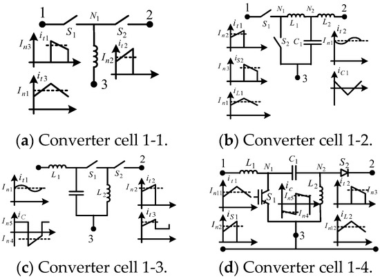
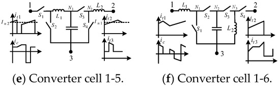
Figure 1.
Converter cells that generate a non-pulsed current signal at one terminal and pulsed current signals at two output terminals.
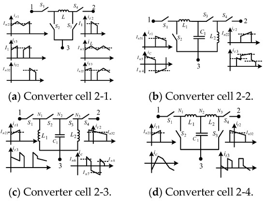
Figure 2.
Converter cells that generate pulsed current signals at all three terminals.
Figure 3.
Converter cells that generate non-pulsed current signals at all three terminals.
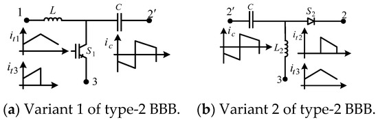
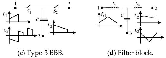
Figure 4.
The other basic building blocks and filter block.
2.2. Unified Analysis of DC–DC Converters Based on Cell 1-1
Figure 5 shows converter cell 1-1 and three of the six possible DC–DC converters derived from converter cell 1-1. Converter cell 1-1 comprises a single type-1 BBB [35]. The current signals generated at the terminals of converter cell 1-1 when operating in CCM are shown in Figure 5 and Figure 6.
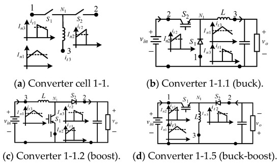
Figure 5.
Converter cell 1-1 and three DC–DC converters derived from it.
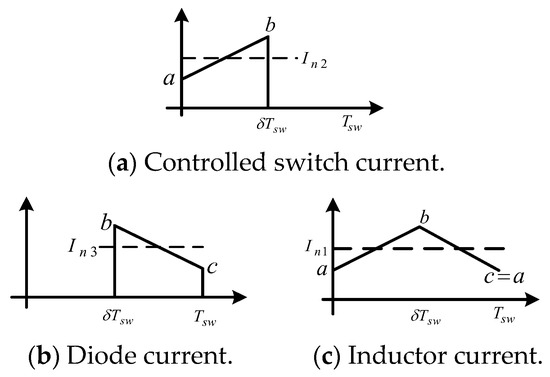
Figure 6.
Current waveforms generated by converter cell 1-1 during CCM.
The Average, RMS, and Ripple RMS Values for Current Signals from DC–DC Converters Based on Cell 1-1
A technique to analyze different converter cells needs to be developed. General expressions for the average, RMS, and RMS ripple values for the various current signals generated by converter cell 1-1 shown in Figure 6 are first derived. The average, RMS, and RMS ripple contents of a periodic current signal, i(t), are obtained using the first mean value theorem as [28,30,31]:
The function describing a signal over one switching period, Tsw, is defined and substituted into (1) to obtain the required values. The input current signals in DC–DC converters 1-1.1 and 1-1.5 comprise a single trapezoidal pulse as shown in Figure 6a. Over one switching period, it is defined as:
Using (1), (2a), and (2b) the average, RMS, and ripple RMS values for the signal in Figure 6a are obtained as
The output current signals in converters 1-1.2 and 1-1.5 comprise of a single trapezoidal pulse, as shown in Figure 6b. Over one switching period, it is defined as
Similarly, using (1), (4a), and (4b) the average, RMS, and ripple RMS values for the signal in Figure 6b are obtained as
The output current in converter 1-1.1 and input current in converter 1-1.2 comprise two trapezoidal pulses as shown in Figure 6c. It can be defined over one switching period as
2.3. Unified Analysis of DC–DC Converters Based on Cell 1-4
The analysis that was introduced in Section 2.2 will now be extended to converter cells realized using type-2 BBBs. This will help to demonstrate that the analysis of current signals can be unified across different converter cells. Specifically, it shows that the analysis is dictated by the type of signals involved and not the converter generating them.
The Average, RMS, and Signal Ripple Content
Figure 7 shows converter cell 1-4 and three of the six possible DC–DC converters derived from the cell. Converter cell 1-4 comprises the two variants of the type-2 BBB [35]. Figure 8 shows the current signals generated at the various terminals of the DC–DC converters derived from converter cell 1-4. These are identical to those for the two variants of type-2 BBB shown in Figure 4. It is seen in Figure 7 and Figure 8 that the functionality of a DC–DC converter does not influence the current signals that the converter generates. Converters 1-4.5 and 1-4.6 are commonly referred to as Sepic and Zeta in the literature.
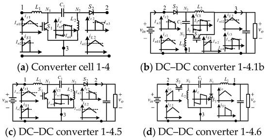
Figure 7.
Converter cell 1-4 and three DC–DC converters derived from it.
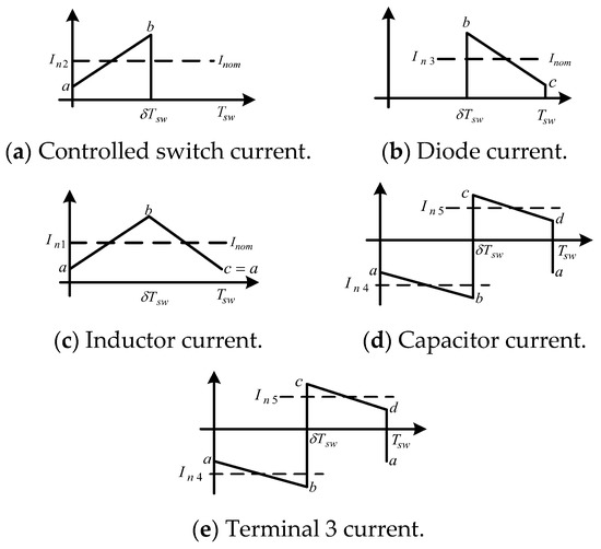
Figure 8.
Current signals generated at various terminals of DC–DC converters derived from cells 1-4.
In deriving (2)–(7), it was shown that signal analysis is a function of the waveform and independent of the type of converter cell generating it. The expressions in (2)–(7) will therefore also be applicable to Figure 8a–c.
The only difference will be in the determination of In = Inom. From Figure 8a,b, the nominal pulse amplitude and pulse amplitude variation are obtained as
For Figure 8c, the nominal pulse amplitude and pulse amplitude variation are obtained as
In order to derive the expressions needed to analyze the signals in Figure 8d,e, the first step is to define them over one switching period. The two signals are similar and hence are described using similar expressions. The current signals can be described using the expressions in (9).
From (1), (9a), and (9b) the average, RMS, and ripple RMS values for signals in Figure 8d,e are obtained as follows:
The expressions in (10a)–(10b) are applicable to terminal three current as well. The only exception is in the values shown in (9b) which should be substituted with those in (10c).
3. Generalized Signal Analysis
This section will show that it is possible to analyze signals from different converter cells and ultimately all non-isolated DC–DC converters in a unified fashion.
3.1. Generalized Analysis of Various Types of Pulses
In Section 2 it was shown that converters built using similar BBBs generate similar current signals. It was also demonstrated that signal analysis is a function of the type of waveforms under investigation. The analysis was thus demonstrated to be applicable to other converter cells.
Current signals generated by non-isolated DC–DC converters can be treated as composite waveforms comprising several unique pulses. In general, these pulses are triangular, rectangular, or trapezoidal. This section will demonstrate that the analysis of the three types of pulses can be treated in a unified fashion by recognizing that the trapezoidal pulse is the most general with the rectangular and triangular being special types of trapezoidal. Furthermore, the orientation of a trapezoidal pulse does not affect the analysis and a single expression is applicable to both positive and negative pulses and also to both positive and negative pulse gradients. Figure 9 shows generalized trapezoidal pulses. The signal duration is from t1 = x1 Tsw until t2 = x2 Tsw where x2 – x1 = δ1, average pulse amplitude I1 = ( + b)/2, and pulse amplitude variation Δi1,pk−pk = (b – ). If = b, they become rectangular; when = 0 and b ≠ 0 or ≠ 0 and b = 0 they become triangular. Furthermore, b > represents a positive gradient and vice-versa. Moreover, < 0 and b < 0 represent a negative pulse while < 0 and b > 0 or > 0 and b < 0 represent a bipolar triangular pulse.
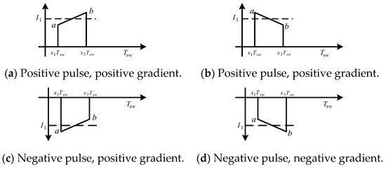
Figure 9.
Generic current pulses.
By recognizing that “” and “b” can assume positive or negative values, all the pulses shown in Figure 9 can be described using the following expression.
This provides the basis for generalizing current signal analysis as the pulses needed to describe a signal as a composite waveform share a common expression. Consequently, expressions for average, RMS, and ripple RMS of the pulses can also be generalized as shown in (12a), (12b), and (12c).
It is seen that (12a), (12b), and (12c) are identical to (3a), (3b), and (3c), respectively, as would be expected.
3.1.1. Analyzing Converters Employing a Type-3 BBB
As converter cells are built using a very small set of BBBs, most converters generate similar current waveforms. Hence, the analysis developed for one converter cell is applicable to other converter cells with similar waveforms. This section will utilize the expressions in (12a)–(12c) to validate this assertion by considering currents in capacitors that employ a type-3 BBB as one of the BBBs.
Current Stress in Converters 2-3.1 and 3-3.1
The DC–DC converters shown in Figure 10a,b have a decoupling capacitor that connects to a node which forms a type-3 BBB. The capacitors’ current signals for a type-3 BBB are shown in Figure 10a–d. Figure 10c,d shows how the shape of the capacitor current waveform changes with load.
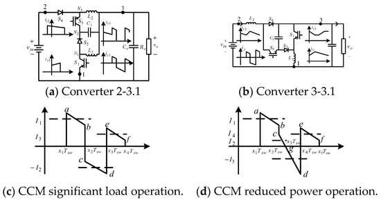
Figure 10.
Some of the group 1 converters and their capacitor current waveforms.
Figure 10c can be partitioned into three unique trapezoidal pulses. The nominal amplitude, amplitude variation, and durations of the pulses are:
Using (12a), (13a), and Figure 10c the signal’s average, RMS, and ripple RMS values are obtained as:
From (13b) and (13c), the signal’s RMS ripple content is
For a capacitor, the RMS and ripple RMS values should be identical as the average value is zero. The waveform in Figure 10d is applicable during CCM light load operation. From Figure 10d, four unique pulses are identifiable (two trapezoidal and two triangular) in each waveform. The nominal amplitude, amplitude variation, and pulses’ durations are:
From (15a) and (15b), the signal’s RMS ripple content is
3.1.2. Converter Cells with Type-2 BBBs
The DC–DC converters shown in Figure 11a,b are realized using at least one type-2 BBB. They generate capacitor currents as shown in Figure 11c,d. It is also seen that the capacitor current waveform changes with load.
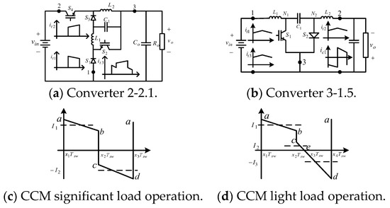
Figure 11.
Some of group 2 converters and their capacitor current waveforms.
The waveform in Figure 11c can be partitioned into two unique trapezoidal pulses. The nominal amplitude, amplitude variation, and durations of the pulses are:
Using (12), (16a), and Figure 11c, the average, RMS, and ripple RMS values are obtained as
From (16b) and (16c), the signal’s RMS ripple content is
The waveform shown in Figure 11d is applicable during a CCM light load operation. Three unique pulses (one trapezoidal and two triangular) are identifiable in Figure 11d. The nominal amplitude, amplitude variation, and durations of the pulses are:
Using (12), (17a), and Figure 11d the capacitor current average, RMS, and ripple RMS values are obtained as:
From (17b) and (17c), the signal’s RMS ripple content is
It is seen that (17d) and (13d) are similar, as expected.
3.2. Generalized Analysis to Cater for Different Types of Signals and Hence a Broad Range of Converters
Considering the generalized composite waveform shown in Figure 12, the expression for the current waveform over one switching cycle is obtained as
Figure 12.
Generalized composite waveform.
The signal’s average, RMS, and ripple RMS values are obtained as
Figure 12 comprises four unique trapezoidal pulses. The pulses’ nominal amplitude, amplitude variation, and durations are:
Substituting (19a) into (18d) yields an expression for RMS current as
Making use of (1), the ripple RMS value is obtained with reference to (18c) and (18b) as
It is seen that (19c) and (15c) are similar, as would be expected.
From (13)–(19), further generalization of expressions for determining the signal’s average, RMS, and ripple RMS values are obtained as
where δn is the normalized duration of the nth pulse.
Expressions in (20) are suitable for analyzing any type of signal generated not only by the various converter cells or any non-isolated DC–DC converter but also by any converter generating waveforms that can be treated as composite waveforms comprising trapezoidal, rectangular, and triangular pulses.
4. Analytical Validation
4.1. Analytical Validation of Derivations
Some examples are presented to analytically validate all the theoretical derivations in particular, to show that analysis is a function of signal shape and can be generalized to cater for any non-isolated DC–DC converter, for example. Figure 13 presents four examples of practical DC–DC converters. Those in Figure 13a,b are derived from converter cell 1-1.w in group 1, whilst that in Figure 13c is derived from converter cell 2-3.w in group 2, and finally the converter in Figure 13d is derived from converter cell 3-3.w in group 3.
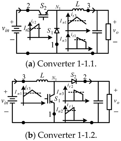
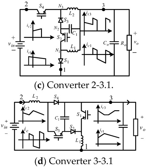
Figure 13.
Examples of DC–DC converters from various converter cells.
Converter Cell 1-1.w Family of Converters
This section will validate the unification of analysis across a family of converters derived from the same converter cell. Conventional buck (converter 1-1.1) and boost (converter 1-1.2) converters based on cell 1-1 are considered. The circuit diagrams are shown in Figure 13a,b while relevant terminals’ current waveforms are shown in Figure 1a, Figure 6a–c, and Figure 13a,b. Current signals generated at terminals 1, 2, and 3 of converter 1-1.1 during CCM operation are as shown in Figure 6a–c, respectively, and also in Figure 13a. The techniques developed in [35] will be employed to determine the converter gains, the nominal amplitudes, In, and variations of pulses’ amplitudes, Δin,pk−pk. Consider the following operating conditions for converter 1-1.1:
From Figure 6 and Figure 13a, the following data applicable to the analysis of signals from converter 1-1.1 are obtained:
Using (3), (20), (21), and Figure 6a and letting , terminal’s two’s current signal is analyzed as follows:
Using (3), (20), (21), and Figure 6c with , , terminal three’s current signal is analyzed as follows:
From (22)–(24), it is seen that (3) and (20) yield identical values for the signal average and RMS values as well as the signals’ ripple RMS values. This demonstrates that the generalized expressions in (20) yield identical results as those in (3) which were derived by considering signals generated by converter cell 1-1.w.
The current signals generated at terminals 1, 2, and 3 of converter 1-1.2 during the CCM operation are as shown in Figure 6a–c, respectively, and also in Figure 13b. Consider the following operating conditions:
From Figure 6 and Figure 13b, the following data applicable to the analysis of the signals from converter 1-1.2 are obtained:
Using (3), (20), (25), and Figure 6a and letting , terminal two’s current signal is analyzed as follows:
Figure 14a,b presents simulated current waveforms it1, it2, and it3 for converters 1-1.1 and 1-1.2, respectively. It is seen from Figure 14a,b that the waveforms are identical to the analytical waveforms shown in Figure 1a, Figure 5a–c, Figure 6a–c, and Figure 8a–c. On the other hand, Table 1 and Table 2 present analytical and simulated data for converters 1-1.1 and 1-1.2, respectively. In particular, the average and RMS values as well as the ripple RMS for the current signals it1, it2, and it3.
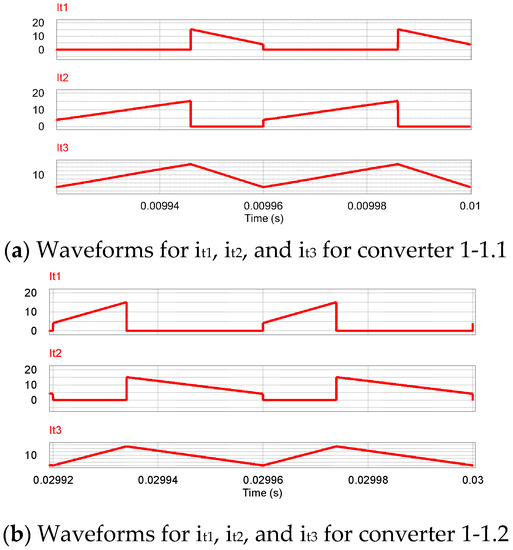
Figure 14.
Current waveforms for converters 1-1.1 and 1-1.2 during CCM.

Table 1.
Analytical and simulated data for converter 1-1.1 when in CCM.
Table 2.
Analytical and simulated data for converter 1-1.2 when in CCM.
From (26)–(28), it is seen that (3) and (20) yield identical signals’ average and RMS values as well as signals’ ripple RMS values. This, together with the analyses in (22)–(24), validates the unification of analysis across a family of DC–DC converters derived from a given converter cell and further validates the generalized analysis in (20). This analysis is valid for operation up to the boundary between continuous and discontinuous inductor current operations.
4.2. Analysis Applicable to Different Types of Converters
This section will demonstrate that the analysis is applicable to any type of non-isolated DC–DC converter. Circuit diagrams for converter cell 2-3.w and a DC–DC converter 2-3.1 with buck–boost functionality are shown in Figure 2c and Figure 13b, respectively. Terminals’ and capacitor current waveforms generated during CCM are shown in Figure 2c, Figure 6a,b, Figure 13c and Figure 15a,b.
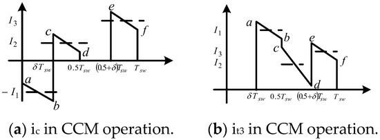
Figure 15.
Capacitor and terminal three current waveforms (ic and it3).
4.2.1. CCM Operation of Converter 2-3.1
Current signals generated at terminals 1, 2, and 3 of converter 2-3.1 as well as converter coupling capacitor current waveform during CCM operation are as shown in Figure 6a,b and Figure 15a,b, respectively. During CCM, operating conditions are as follows:
The capacitor current signal shown in Figure 15a can be divided into three unique trapezoidal pulses (i.e., k = 3). The following data are relevant to the capacitor current signal:
The nominal pulse amplitudes, durations, and amplitude variations are obtained using (33a) and Figure 15a as:
Figure 16a presents simulated current waveforms it1, it2, and it3. Figure 16b, on the other hand, presents current waveforms for the coupling capacitor, ic, inductor L1, iL1, and inductor L2, iL2, for converter 2-3.1. It is seen from Figure 16 that the simulated waveforms are similar to the analytical waveforms shown in Figure 2c, Figure 5a–c, Figure 6a–c, and Figure 8a–e and which were used to derive the analytical expressions. On the other hand, Table 3 presents analytical and simulated data relevant to converter 2-3.1. In particular, the average and RMS values as well as ripple RMS values for the current signals it1, it2, it3, and ic.
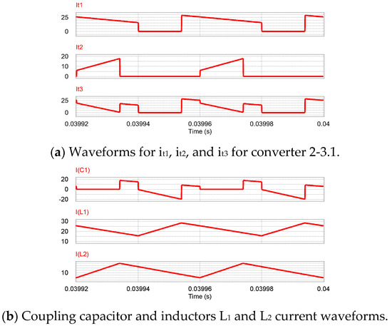
Figure 16.
Various current waveforms for converter 2-3.1.
Table 3.
Analytical and simulated date for converter 2-3.1 under CCM.
From (30)–(35) and Table 3, it is seen that expressions in (24) yield accurate signal averages and RMS values as well as signals’ ripple RMS values. The good agreement between analytical and simulated values validates the accuracy of the analytical techniques that were developed.
4.2.2. CCM Operation of Converter 3-3.1
Current signals generated at terminals one, two, and three of converter 3-3.1 and current through the decoupling capacitor during CCM operation are as shown in Figure 6c and Figure 17a,b, respectively.
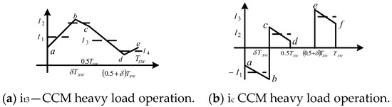
Figure 17.
Converter 3-3.1terminal 3 and capacitor current waveforms.
Consider a converter that is operating under the following conditions:
From (35a) and Figure 6c, the following data are relevant to it1 and it2:
From (20), (35a), (35b), and Figure 6c with , the average, RMS, and ripple RMS values for signal it1 are obtained as follows:
Figure 18a shows the current waveforms generated at the three output terminals of converter 3-3.1. Figure 18b, on the other hand, shows the current waveforms for the coupling capacitor and controlled switches S1 and S3. It is seen that these waveforms are in agreement with the analytical waveforms shown in Figure 4c, Figure 10b, and Figure 13d and which were used to derive the analytical expressions.
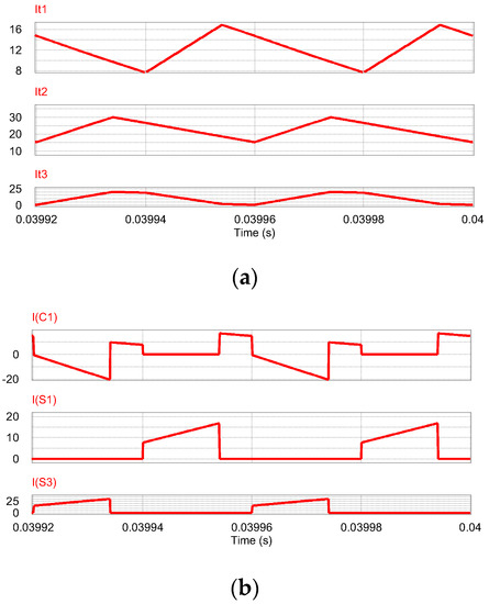
Figure 18.
Current waveforms at output terminals and through some of the components of converter 3-3.1. (a) Current waveforms for it1, it2, and it3; (b) Coupling capacitor and switches S1 and S3 current waveforms.
Table 4 presents analytical and simulated data relevant to the analysis of current signals generated by converter 3-3.1. In particular, the nominal amplitudes of various current pulses, variations of the pulses’ nominal amplitudes, signals it1, it2, it3, and ic average and RMS values, and the signals’ ripple content RMS values. The simulated data are used to validate those derived analytically and in turn validate the accuracy of the analytical techniques that were developed.
Table 4.
Analytical and simulated data for converter 3-3.1 under CCM.
From (35)–(39) and Table 4 it is seen that expressions in (20) yield accurate values for signal averages and RMS values as well as signals’ ripple RMS values. There is good agreement between analytical and simulated values. This validates the accuracy of the analytical technique that was developed.
5. Conclusions
The analysis of current stress in various components of any DC–DC converter is needed to evaluate losses and size components. At the moment, the analysis of current signals is treated as unique to a given DC–DC converter. However, recent studies have shown that there is a set of three three-terminal BBBs and a three-terminal filter block which between them, are sufficient for realizing all non-isolated DC–DC converters without coupled inductors. Additionally, these BBBs generate unique current signals at their terminals.
This paper has shown that the analysis of current signals is a function of the signals’ shape and is independent of the converter topology. The study also demonstrated that current signals generated by DC–DC converters can be treated as composite waveforms comprising triangular, rectangular, trapezoidal, or a combination of these pulses. The triangular and rectangular pulses were shown to be special cases of the trapezoidal pulse. Consequently, generalized analysis of any signal was possible based on the analysis of a generalized trapezoidal pulse. A generalized expression that allows the direct evaluation of current signal ripple content without the need to first evaluate signal average and RMS values (as is currently the case) was derived.
Author Contributions
Conceptualization, M.N.G., G.P.A. and L.M.; methodology, M.N.G. and L.M.; software, M.N.G., G.P.A. and L.M.; validation, L.M. and M.N.G.; formal analysis, M.N.G. and L.M.; investigation, M.N.G., G.P.A., L.M. and M.N.G.; data curation, M.N.G.; writing—original draft preparation, M.N.G.; writing—review and editing, G.P.A., L.M. and M.N.G.; visualization, L.M. and M.N.G.; project administration, G.P.A., L.M. and M.N.G. All authors have read and agreed to the published version of the manuscript.
Funding
This research received no external funding.
Data Availability Statement
All generated data are contained in the manuscript.
Conflicts of Interest
The authors declare no conflict of interest. The funders had no role in the design of the study; in the collection, analyses, or interpretation of data; in the writing of the manuscript; or in the decision to publish the results.
References
- Zheng, F.; Zhong, R.; Xie, W.; He, J.; Xia, Y.; Xue, F. Research on AC-DC hybrid power supply system in industrial park. In Proceedings of the 16th IET International Conference on AC and DC Power Transmission, Online, 2–3 July 2020. [Google Scholar]
- Ji, H.; Wang, D.; Xu, Q.; Yuan, S.; Cai, Y.; Lei, X. DC power distribution system and its protection configuration. In Proceedings of the 2021 6th international Conference on Power and Renewable Energy (ICPRRE), Shanghai, China, 17–20 September 2021; pp. 582–587. [Google Scholar]
- Zhao, X.; Yang, G.; Bai, X.; Yang, Z.; Yang, G. Construction of low voltage DC smart buildings with generation-storage-distribution-utilization. In Proceedings of the 2021 IEEE Sustainable Power and Energy Conference, Nanjing, China, 22–25 December 2021; pp. 2140–2143. [Google Scholar]
- Zhang, W.; Liu, Y.; Cui, Y.; Zhao, M.; Wei, T.; Chen, Q. Research on typical power supply mode of DC distribution and consumption system. In Proceedings of the 2020 IEEE Sustainable Power and Energy Conference, Chengdu, China, 23–25 November 2020; pp. 491–496. [Google Scholar]
- Cho, J.; Cho, Y.; Kim, H.; Kim, H.; Kim, J.; Kim, H. A new protection scheme using an AC-DC converter for a LVDC distribution system. In Proceedings of the IEEE 3rd International Conference on DC microgrids (ICDCM), Matsue, Japan, 20–23 May 2019. [Google Scholar]
- Xie, W.; Zhong, R.; Xia, Y.; Xue, F.; He, W. Study on grounding method of DC system in an AC and DC hybrid power system of industrial park. In Proceedings of the 2020 IEEE Asia Energy and Electrical Engineering Symposium, Chengdu, China, 29–31 May 2020; pp. 285–290. [Google Scholar]
- Li, J.; Ertao, L.; Kai, M.A.; Zhenpeng, L.; Hua, H.; Hao, Y. Comparative analysis of DC distribution schemes for low-voltage control at the end of the grid. In Proceedings of the 2021 IEEE Sustainable Power and Energy Conference, Nanjing, China, 22–25 December 2021; pp. 2840–2845. [Google Scholar]
- Kolar, J.W.; Wolbank, T.M.; Schrodl, M. Analytical calculation of RMS current stress on the DC-link capacitor of voltage DC link PWM converter system. In Proceedings of the 9th International Conference on Electrical Machines and Drives, Canterbury, UK, 1–3 September 1999; pp. 81–89. [Google Scholar]
- Gohil, G.; Bede, L.; Teodorescu, R.; Blaabjerg, F. Analytical method to calculate the DC link current stress in voltage source converters. In Proceedings of the 2014 IEEE PEDES Conference Proceedings, Mumbai, India, 16–19 December 2014. [Google Scholar]
- Ahmad, S.S.; Narayanan, G. Evaluation of DC-link capacitor RMS current in switched reluctance motor drives. IEEE Trans. Ind. Appl. 2021, 57, 1459–1471. [Google Scholar] [CrossRef]
- Ippisch, M.; Gerling, D. Calculation of active and passive components stress of multiphase inverters with single-frequency output. In Proceedings of the IEEE Transportation Electrification Conference and Expo, Chicago, IL, USA, 23–26 June 2020; pp. 420–426. [Google Scholar]
- Mazumder, S. Complete mathematical analysis of ripple current as a function of the modulation index for direct-indirect and bus clamped space vector modulation techniques. In Proceedings of the IEEE International Electric Machines and Drives Conference Record, Milwaukee, WI, USA, 18–21 May 1997. [Google Scholar]
- Chen, B.; Su, H. Current stress analysis of passive devices and switching devices of quasi-Z-source inverters. In Proceedings of the IEEE 2021 6th Asia Conference on Power and Electrical Engineering, Chongqing, China, 8–11 April 2021; pp. 1461–1465. [Google Scholar]
- Nishizawa, K.; Itoh, J.-I.; Odaka, A.; Toba, A.; Umida, H.; Fujita, S. Current stress reduction for DC-link capacitors of three-phase VSI with carrier based continuous PWM. IEEE Trans. Ind. Appl. 2019, 55, 6061–6072. [Google Scholar] [CrossRef]
- Grbovic, P.J. Closed-form analysis of N-cell interleaved two-level DC-DC converters: The DC-bus capacitor current stress. In Proceedings of the IEEE ECCE Asia Downunder, Melbourne, VIC, Australia, 3–6 June 2013; pp. 122–129. [Google Scholar]
- Rudenko, Y. Analysis of DC-DC converters by averaging method based on Lagrange theorems. In Proceedings of the 2021 IEEE 2nd KhPI Week on Advanced Technology, Kharkiv, Ukraine, 13–17 September 2021; pp. 367–370. [Google Scholar]
- Zhuo, S.; Gaillard, A.; Li, Q.; Ma, R.; Paire, D.; Gao, F. Current ripple optimisation for four-phase floating interleaved DC-DC boost converter under switching fault. IEEE Trans. Ind. Appl. 2020, 56, 4214–4224. [Google Scholar] [CrossRef]
- Chang, C. Current ripple bounds in interleaved DC-DC power converters. In Proceedings of the IEEE International Conference on Power Electronics and Drive Systems, Singapore, 21–24 February 1995; pp. 738–743. [Google Scholar]
- Tymerski, R.; Li, D. Extended ripple analysis of PWM DC-DC converters. IEEE Trans. Power Electron. 1993, 8, 588–595. [Google Scholar] [CrossRef]
- Carlos, J.; Floriani, A. Generalised analysis of current ripple in PWM H-bridge converter with unipolar-bipolar switching. IEEE Power Electron. Lett. 2004, 2, 83–86. [Google Scholar]
- Dahono, P.A.; Riyadi, S.; Mudawari, A.; Haroen, Y. Output ripple analysis of multiphase DC-DC converters. In Proceedings of the Intenaional Conference on Power Electronics and Drive Systems (PEDS), Hong Kong, China, 27–29 July 1999; pp. 626–630. [Google Scholar]
- El Khateb, H.; Rahim, N.A.; Selvaraj, J.; Williams, B.W. DC-DC converter with low input current ripple for maximum photovoltaic power extraction. IEEE Trans. Ind. Electron. 2015, 62, 2246–2256. [Google Scholar] [CrossRef]
- Williams, B.W. DC-DC converters with continuous input and output power. IEEE Trans. Power Electron. 2013, 28, 2307–2316. [Google Scholar] [CrossRef]
- Hu, Y.; Wu, J.; Cao, W.; Xiao, W.; Li, P.; Finney, S.J.; Li, Y. Ultrahigh step-up DC-DC converter for distributed generation by three degrees of freedom approach. IEEE Trans. Power Electron. 2016, 31, 4930–4941. [Google Scholar]
- Mouli, G.R.C.; Schijffelen, J.H.; Bauer, P.; Zeman, M. Design and comparison of a 10-kW interleaved boost converter for PV application using Si and SiC devices. IEEE J. Emerg. Sel. Top. Power Electron. 2017, 5, 610–623. [Google Scholar] [CrossRef]
- EPCOS Aluminium Electrolytic Capacitors with Screw Terminals Series B43742, B42762, December 2019. Available online: https://www.tdk-electronics.tdk.com/en/529316/products/products-catalog/aluminium-electrolytic-capacitors/capacitors-with-screw-terminal (accessed on 10 December 2022).
- CDM Cornell Dubilier DCMC Electrolytic Capacitors Datasheets. Available online: https://www.cde.com/capacitors/aluminium-electrolytic/screw-terminal (accessed on 10 December 2022).
- Jeffrey, A. Mathematics for Engineers and Scientists; English Language Book Society and Thomas Nelson and Sons Ltd.: London, UK, 1971. [Google Scholar]
- Shahir, F.M.; Babaei, E.; Aberoumandazar, M. New single-switch non-isolated boost DC-DC converter with free input current ripple. In Proceedings of the Power electronics, Drive Systems and Technologies (PEDSTC) Conference, Tabriz, Iran, 2–4 February 2021. [Google Scholar]
- Mohan, N.; Undland, T.M.; Robbins, W.P. Power Electronics: Converters, Applications and Design, 2nd ed.; Wiley: New York, NY, USA, 1995. [Google Scholar]
- Erickson, R.W. Fundamentals of Power Electronics; Chapman and Hall: New York, NY, USA, 1997. [Google Scholar]
- Gitau, M.N.; Hofsajer, I.W. Analysis of 4-phase tapped-inductor DC-DC boost converter for high boost ratio wide voltage range applications. In Proceedings of the IEEE IECON Conference Proceedings, Dallas, TX, USA, 29 October–1 November 2014; pp. 5468–5474. [Google Scholar]
- Muchina, E.G.; Masike, L.; Gitau, M.N. High boost-ratio bidirectional converter for interfacing low-voltage battery energy storage system to a DC bus. IET Power Electron. 2019, 12, 2372–2381. [Google Scholar] [CrossRef]
- Hashmzadeh, S.M.; Marzang, V.; Pourjafar, S.; Hosseini, S.H. An ultra high step-up dual-input single ouput DC-DC converter based on coupled inductor. IEEE Trans. Ind. Electron. 2022, 69, 11023–11034. [Google Scholar] [CrossRef]
- Tymerski, R.; Vorperian, V. Generation and classification of PWM DC-DC converters. IEEE Trans. Aerosp. Electron. Syst. 1988, 24, 743–754. [Google Scholar] [CrossRef]
- Gitau, M.N.; Adams, G.P.; Masike, L.; Mbukani, M.K. Unified approach to synthesis and analysis of non-isolated DC-DC converters. IEEE Access 2021, 9, 120088–120109. [Google Scholar] [CrossRef]


Disclaimer/Publisher’s Note: The statements, opinions and data contained in all publications are solely those of the individual author(s) and contributor(s) and not of MDPI and/or the editor(s). MDPI and/or the editor(s) disclaim responsibility for any injury to people or property resulting from any ideas, methods, instructions or products referred to in the content. |
© 2023 by the authors. Licensee MDPI, Basel, Switzerland. This article is an open access article distributed under the terms and conditions of the Creative Commons Attribution (CC BY) license (https://creativecommons.org/licenses/by/4.0/).