Abstract
Silicon carbide (SiC)-based metal–oxide–semiconductor field-effect transistors (MOSFETs) hold promising application prospects in future high-capacity high-power converters due to their excellent electrothermal characteristics. However, as nascent power electronic devices, their long-term operational reliability lacks sufficient field data. The power cycling test is an important experimental method to assess packaging-related reliability. In order to obtain data closest to actual working conditions, forward power cycling is utilized to carry out SiC MOSFET degradation experiments. Due to the wide bandgap characteristics of SiC MOSFETs, the short-term drift of the threshold voltage is much more serious than that of silicon (Si)-based devices. Therefore, an offline threshold voltage measurement circuit is implemented during power cycling tests to minimize errors arising from this short-term drift. Different characterizations are performed based on power cycling tests, focused on measuring the on-state resistance, thermal impedance, and threshold voltage of the devices. The findings reveal that the primary failure mode under forward power cycling tests, with a maximum junction temperature of 130 ∘C, is bond-wire degradation. Conversely, the solder layer and gate oxide exhibit minimal degradation tendencies under these conditions.
1. Introduction
In the pursuit of global efforts toward developing clean energy sources, the proportion of renewable energy sources, including wind and photovoltaic power, in the power grid is escalating, paralleled by a remarkable surge in the installed capacity of these units [1,2]. According to the latest data released by the International Energy Agency (IEA) in June 2023, global renewable energy capacity additions are anticipated to surge to 550 GW in 2024, necessitating the integration of an increasing amount of renewable energy into the grid via converters. This extensive and high-capacity integration of renewable energy imposes stringent performance criteria on converters [3], particularly in terms of their efficiency [4], reliability [5], and active support capabilities [6].
In the novel operational setting, the switching loss of the converter assumes a pivotal role as a critical quality factor, accounting for an increasing percentage of the overall loss due to high-frequency switching operations [7]. Silicon carbide (SiC) metal–oxide–semiconductor field-effect transistors (MOSFETs) offer a substantial edge over silicon (Si) insulated-gate bipolar transistors (IGBTs), exhibiting a remarkable 2.86-fold reduction in switching losses across the same frequency range [8]. Furthermore, SiC MOSFETs boast not only lower switching losses but also reduced conduction losses compared to Si MOSFETs [9]. Theoretically, under equivalent withstand voltage, the drift layer resistance per unit area of SiC can be significantly diminished up to 300 times lower than Si [10]. Additionally, Si-based devices have encountered their inherent physical constraints in terms of blocking voltage, making them insufficient for the upcoming era of high-voltage DC transmission lines, which typically boast rated voltages reaching up to 800 kV [11]. In contrast, SiC devices exhibit a significantly superior blocking capability, allowing systems that employ these devices to reduce the number of components required in series submodule units [12] and affiliated auxiliary electronic components [4,13]. This, in turn, leads to a further miniaturization of the converter. Furthermore, SiC material possesses the inherent advantage of being able to operate at elevated temperatures, unlike Si [14]. By capitalizing on these advantages, SiC MOSFETs demonstrate exceptional performance in high-temperature, high-frequency, and high-voltage applications [15]. However, despite the numerous benefits of SiC MOSFETs, their long-term reliability issues, as an emerging power electronic device, still necessitate in-depth research and solutions [16].
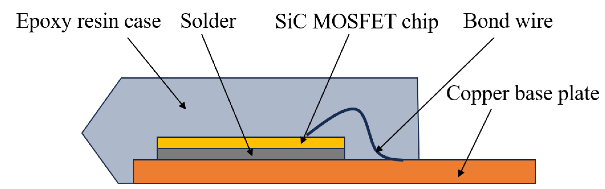
Power electronic devices consist of materials exhibiting diverse coefficients of thermal expansion (CTE), as depicted in Figure 1. Temperature fluctuations within high-temperature, high-frequency, and high-voltage operating environments give rise to internal thermal stresses, resulting in degradation phenomena such as cracks. These cracks ultimately limit the device’s lifespan [17]. In practical working conditions, device failure is a gradual process that occurs over an extended period. Consequently, in experimental research, the power cycling test (PCT) method is frequently utilized to expedite the failure process. The PCT is designed to simulate the thermo-mechanical stresses imposed on power electronic devices in their actual operating environments, enabling the investigation of component failures [18].
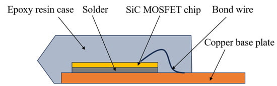
Figure 1.
Cross-sectional view of TO-247 packaged SiC MOSFET.
This paper aims to conduct a thorough investigation into the performance evolution of SiC MOSFETs under specific power cycling conditions, analyzing the underlying failure mechanisms through a systematic series of experimental studies. To establish a solid foundation, this paper begins with a concise overview of failure experiments conducted under power cycling conditions. This overview includes elucidating the fundamental failure principles of the device, discussing various experimental methodologies employed in power cycling, describing calibration procedures for temperature-sensitive parameters, and explaining the measurement techniques used to assess thermal impedance. Subsequently, a detailed description of the experimental methodology is presented. To accurately measure the variation in its threshold voltage, an offline threshold voltage measurement circuit is utilized, mitigating the short-term drift value arising from the wide bandgap characteristics of SiC [19]. Furthermore, to precisely monitor the junction-to-case thermal impedance and identify the aging state of the solder layer, a thermal characterization experiment is conducted based on JESD51-14 [20]. In the final section, the experimental results are comprehensively analyzed, delving into the exploration of potential failure mechanisms. Additionally, a brief discussion is presented regarding strategic measures to enhance the reliability of SiC MOSFETs.
2. Background
2.1. Main Failure Modes and Characterization Parameters
Device failures primarily include chip-level failures and package-level failures [21], as shown in Table 1. Chip-level failures manifest as gate oxide failures and body diode failures. Gate oxide failures are generally caused by interfacial charge or breakdown effects induced by electrical overstress and high temperatures [22,23], whereas body diode failures mainly stem from forward voltage bias stress [24].

Table 1.
Main failure modes of SiC MOSFETs and their characterization parameters.
Currently, widely employed indicators for gate oxide failure [25] include various parameters such as the miller plateau voltage amplitude () [26], miller plateau duration () [26], on-state resistance () [27], drain leakage current () [28], threshold voltage () [22,29], and gate leakage current () [30], among others. These indicators provide crucial insights into the health and degradation of the gate oxide layer. When it comes to characterizing body diode degradation, key parameters mainly include the on-state resistance of the body diode () [31], forward voltage () [32], and drain leakage current () [33].
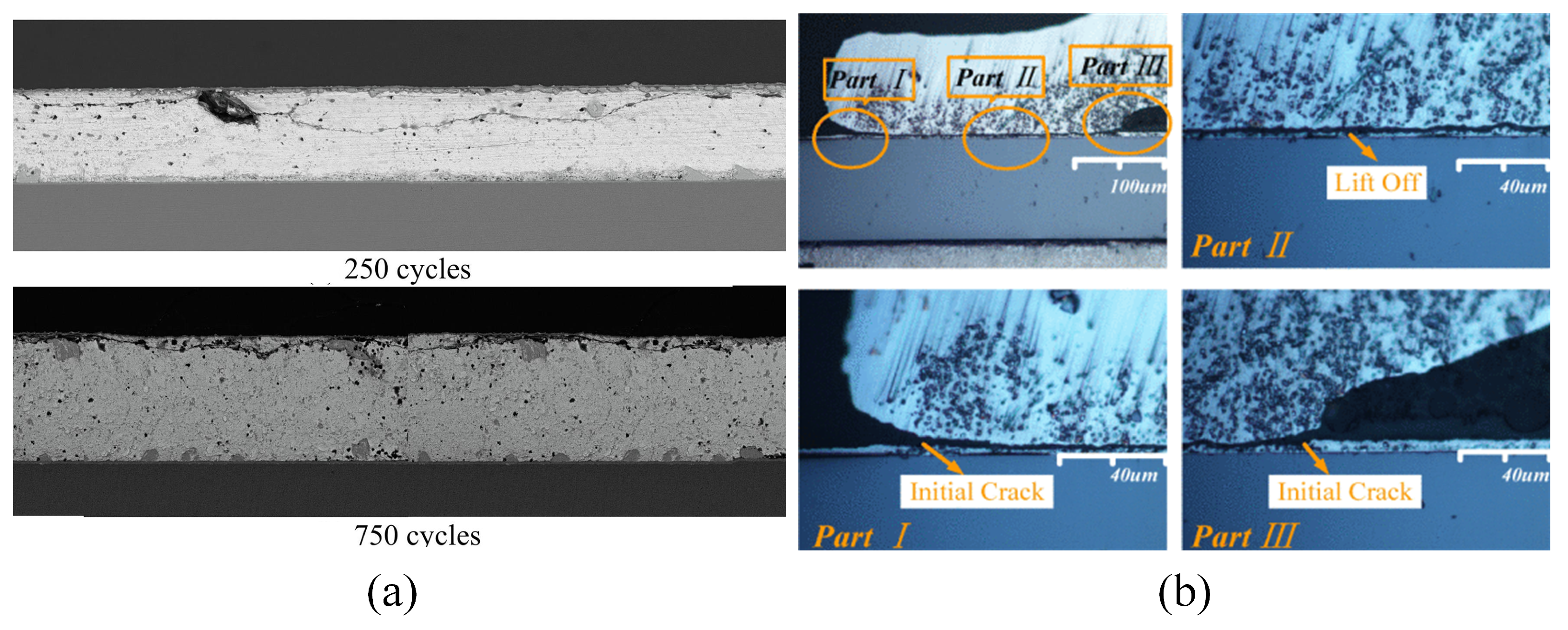
Common package-level failures for devices mainly comprise bond-wire failures and solder fatigue [34], as shown in Figure 2. This type of failure primarily stems from thermo-mechanical stresses [35], relative humidity stresses [36], and high current density stresses [37] during device operation, with thermo-mechanical stresses being dominating.

Figure 2.
Package level Failure. (a) Crack failure in the solder layer [38]. (b) Bond wire crack and lift-off failure [39].
There are two main failure mechanisms of bond wires [40]. One is caused by the difference in CTEs between the bond wire and the SiC chip, leading to crack formation and eventually bond-wire lift-off [41,42]. Heel cracking is the second failure mode, which comes from the thermo-mechanical stresses generated by heat transfer within the bond wire and the displacement between the two bond pads due to the overall CTE mismatch [43]. The failure modes of bond wires are related to their aspect ratios, and studies have indicated that bond wires with different aspect ratios have different failure modes [44]. They primarily affect the conduction current path; thus, the key characterization parameters are the on-state voltage () and on-state resistance (). In the literature [45], the on-state voltage is used as an indicator for bond-wire lift-off. Standard AQG324 [46] states that the device is considered to have reached a failure criterion when the on-state voltage increases by more than 5% of its initial value.
Solder fatigue is mainly due to differences in CTEs between the solder and the connected materials, as well as between different pads, resulting in solder delamination [47,48]. Solder fatigue primarily affects the thermal conduction path, where cracks and voids reduce the effective thermal conduction area between the chip and copper board, leading to changes in thermal impedance () between them [49]. In Ref. [50], thermal impedance was used as a characterization parameter for solder fatigue under narrow temperature fluctuations, and in [51] B. Ji et al. carried out fatigue state monitoring of solder layers in IGBT modules using thermal impedance as a parameter. Standard AQG324 [46] mentions that the failure criterion for thermal impedance is a growth to 20% of the initial value.
2.2. Power Cycling Test Modes
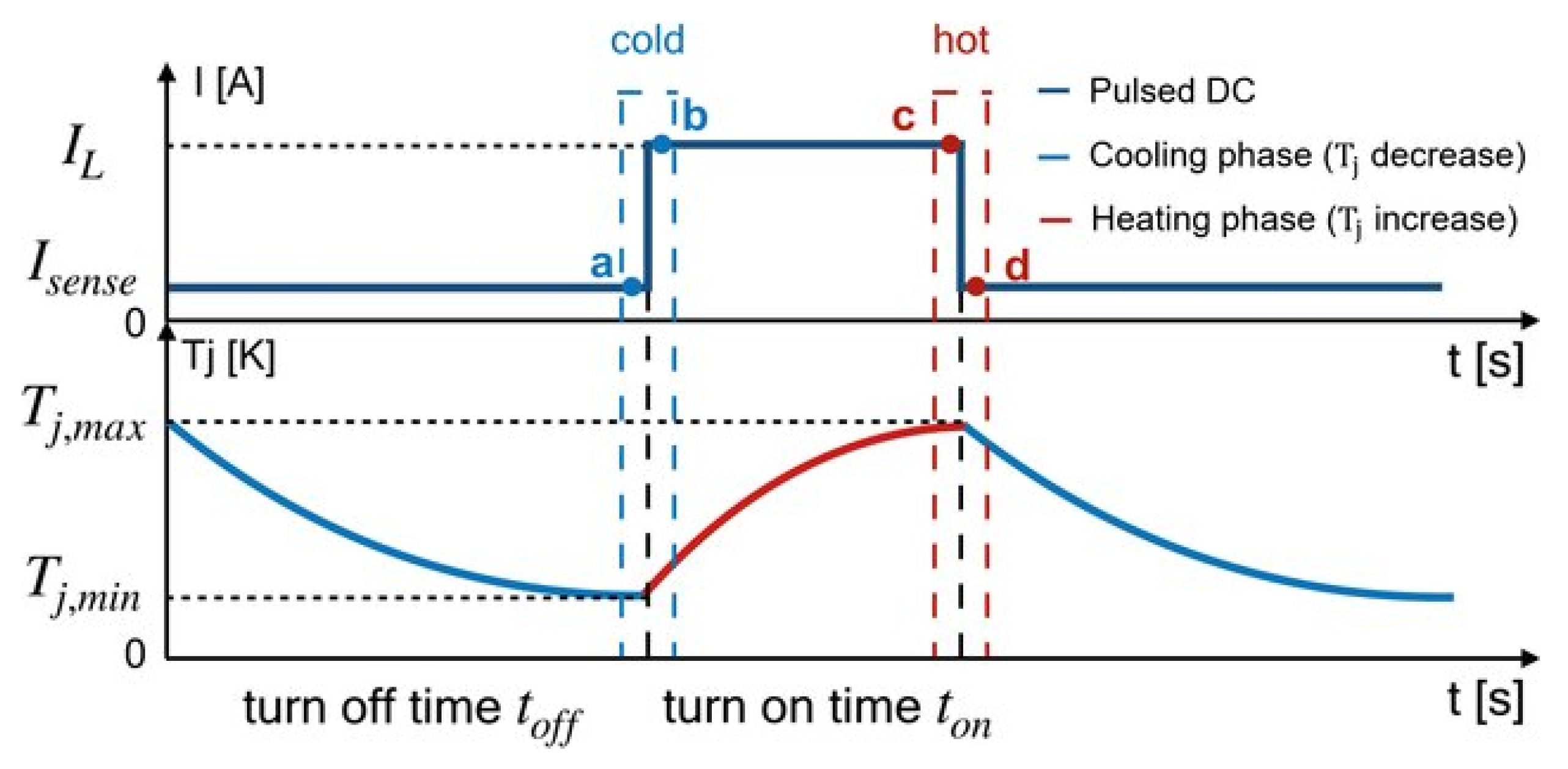
The PCT is a rapid experimental method used to induce failure in research devices. As shown in Figure 3, it heats and cools the device with cyclic load currents (), and during the cooling phase, a small sense current () is applied for parametric measurements. This repeated heating and cooling creates thermo-mechanical stresses within the device, causing cumulative fatigue and accelerated aging.
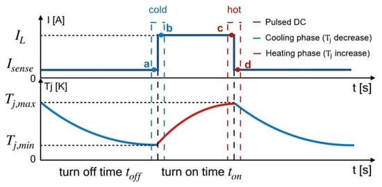
Figure 3.
Power cycling test procedure [52].
The PCT can be classified into DC and AC versions, distinguished primarily by the nature of the heating current. Despite their common failure modes [53], the DC method stands out due to its simplicity in control, making it the preferred option. Regarding heat generation mechanisms, three distinct modes of power cycling exist: forward mode, reverse mode, and body diode mode. In forward mode, heat is primarily generated by the forward on-state resistance during the device’s on state. Conversely, in reverse mode, heat generation arises from both the reverse on-state resistance and the body diode while the device is in its on state. Finally, the body diode mode specifically involves heat generation solely by the body diode when the device is in its off state. It is noteworthy that the latter two modes are influenced by the negative temperature coefficient of the body diode, resulting in deviations from the typical operational behavior of SiC MOSFETs in practical scenarios [54]. Consequently, the forward mode is generally preferred.
The control strategies for power cycling mainly encompass four types [55], as shown in Table 2.
Table 2.
Four power cycling test strategies.
In practical applications, compensating for attenuation by reducing output power is generally unacceptable [56]. Consequently, the PCT without attenuation compensation is the preferred approach, and this experiment employs the active mode along with a control strategy that maintains a constant switching time.
2.3. Junction Temperature Measurement
There are two primary categories of measurement methods for the device junction temperature: invasive and non-invasive methods. Invasive methods necessitate direct or indirect contact with the chip, necessitating the opening of the package during measurement. However, this process can potentially damage the chip, thereby compromising the experiment’s outcomes. Conversely, non-invasive methods eliminate the need for chip contact and indirectly measure the junction temperature through other parameters. These methods are outlined in Table 3.
Table 3.
Junction temperature measurement methods.
The temperature-sensitive electrical parameter (TSEP) method is the most commonly used method to characterize junction temperature changes at this stage. The choice of parameters should meet several criteria, including a linear relationship with the junction temperature, ease of measurement, and independence from device aging. Currently, the mainstream junction TSEPs include the forward voltage drop of the body diode under low current, on-state resistance, and threshold voltage.
The on-state resistance [60], while serving as a notable indicator of device aging, exhibits a significant drift in its relationship with the junction temperature curve following device failure. Regarding the threshold voltage [61], its value experiences considerable fluctuations during measurement due to the presence of traps within the device. Consequently, accurately determining whether these fluctuations are attributed to traps or temperature changes becomes challenging, as uncontrollable factors exert a significant influence. In contrast, the body diode exhibits excellent stability and high sensitivity during the aging process of the device, with its characteristics remaining unchanged over time [62]. Therefore, the voltage drop across the body diode under low current conditions was chosen as the TSEP.
2.4. Thermal Impedance Measurement
Thermal impedance measurements, crucial for characterizing solder layer failures in package-level failures, remain a pivotal research area.
Conventional methods for measuring thermal impedance adhere to the JESD 51-1 standard, which necessitates concurrent measurements of the junction temperature, case temperature, and power dissipation. However, this standard lacks clarity regarding whether the case temperature should be represented as an average or a maximum value [63]. Furthermore, when the device is mounted on a heatsink, accurately gauging the device’s external case temperature necessitates drilling a small hole in the heatsink for thermocouple placement, potentially perturbing the temperature field.
In [64], a method for evaluating heating curves was proposed, but it still does not determine the thermal interface resistance between the package case surface and the heatsink. Building on this, Szabo et al. [65,66] proposed to compare the structure functions obtained from two transient measurements at different interface layers between the case and the heatsink to identify the thermal impedance, known as the transient dual-interface measurement (TDIM), but the structure-function composition is not very accurate. Schweitzer [67] provided an alternative assessment method for the TDIM based on the derivative of the curve. This eventually led to the development of JESD51-14 [20], which defines the TDIM and its measurement method.
3. SiC MOSFET Degradation Experiment
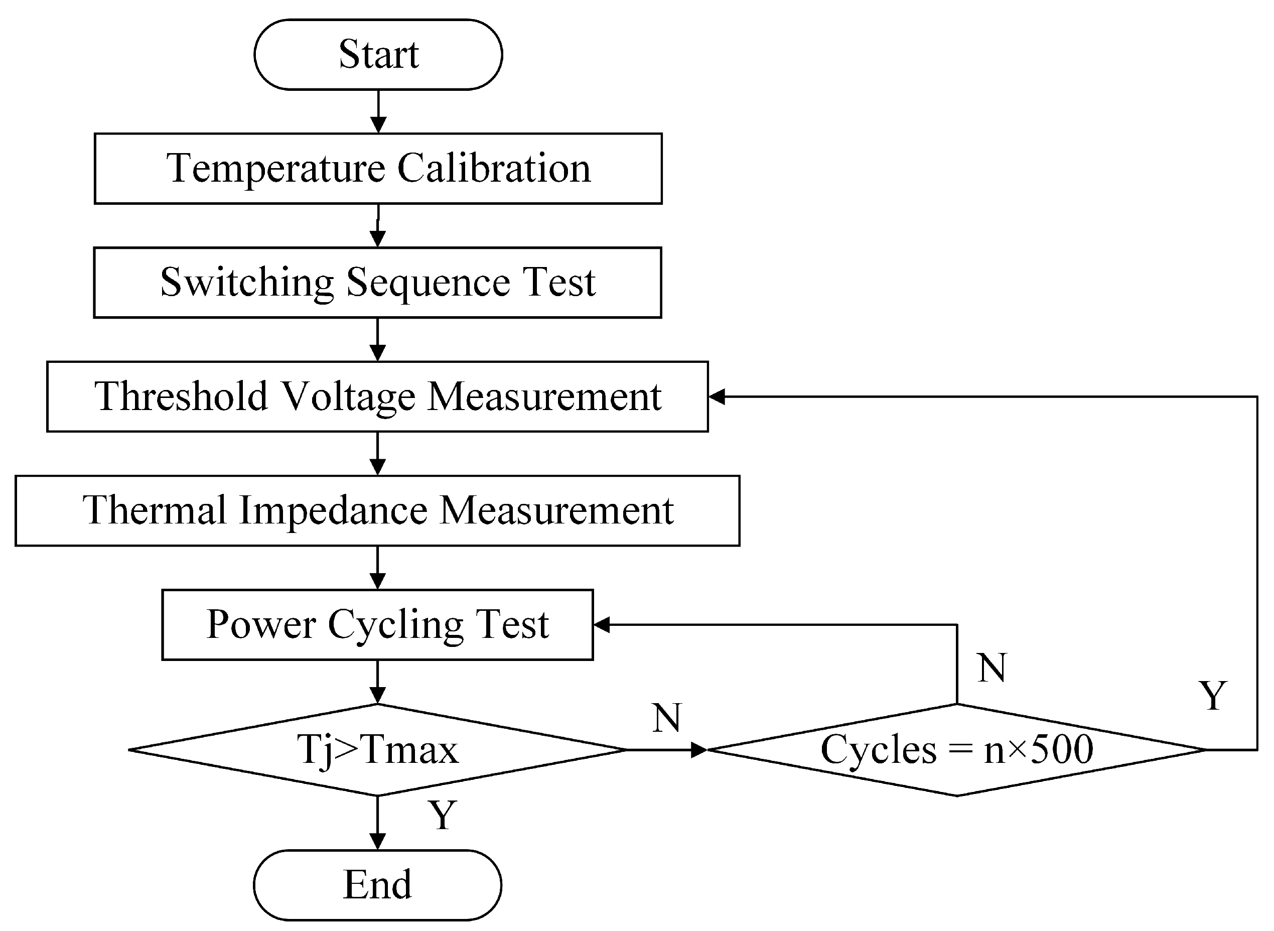
Two device types, C2M0080120D with multiple bond wires (Wolfspeed, Durham, NC, USA) and SCT30N120 with a single bond wire (STMicroelectronics, Geneva, Switzerland), were utilized for the power cycling test to compare the performance of devices with single bond-wire and multiple bond-wire configurations. Table 4 summarizes the key characteristics of the devices used. Given the significance of real-time temperature monitoring in the experiment, calibration tests were conducted on the TSEP prior to commencing the experiment. Furthermore, we optimized the control sequence to minimize noise and overvoltage generation during the PCT. Additionally, to ensure accurate threshold voltage measurements, a pre-study was conducted using an offline approach to mitigate the short-term drift of the threshold voltage. Lastly, emphasis was placed on accurate and reliable measurements of the thermal impedance. Offline measurements of the threshold voltage and thermal impedance were performed every 500 or 2000 cycles, and a detailed experimental flowchart is presented in Figure 4.
Table 4.
Main characteristics of DUTs.
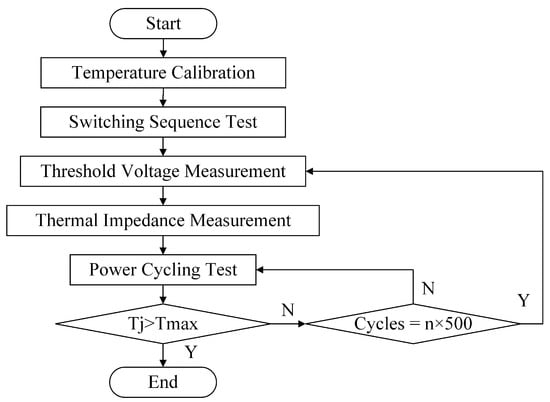
Figure 4.
Flowchart of SiC MOSFET degradation experiment.
3.1. Temperature Estimation Using the TSEP
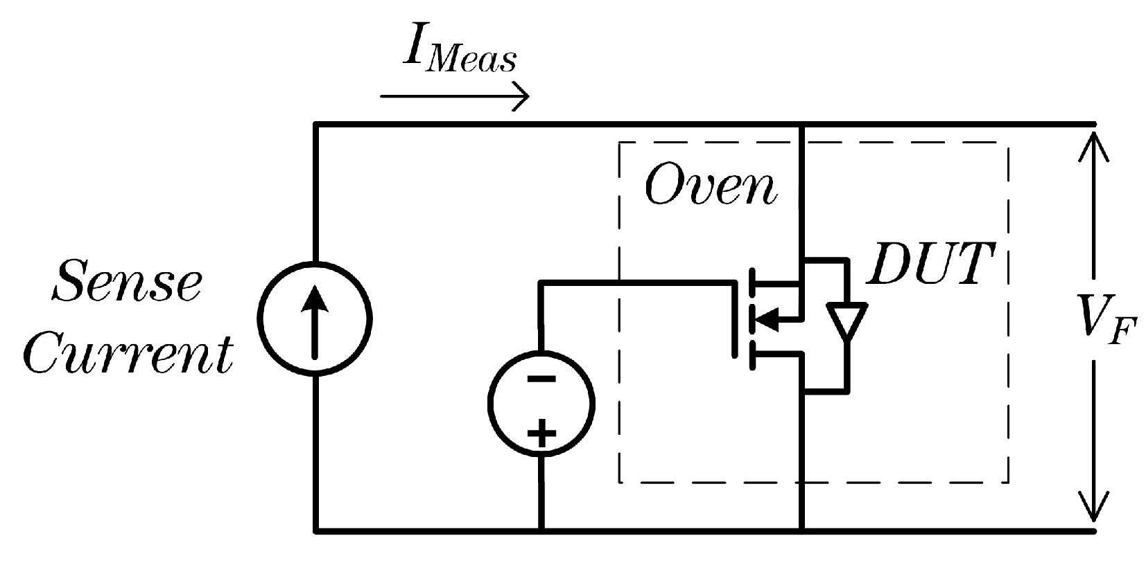
The junction temperature was measured using the body diode voltage drop as the TSEP, and the calibration circuit is shown in Figure 5. After the temperature in the oven reached a steady state, a sense current was applied to measure the voltage drop across the body diode. To minimize the self-heating effect caused by the sense current, the sense current was applied in the form of pulses. The device’s drain-to-source voltage was measured as the voltage drop across the body diode at this temperature.
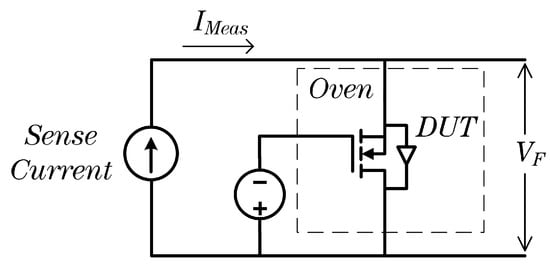
Figure 5.
Circuit diagram of junction temperature calibration experiment.
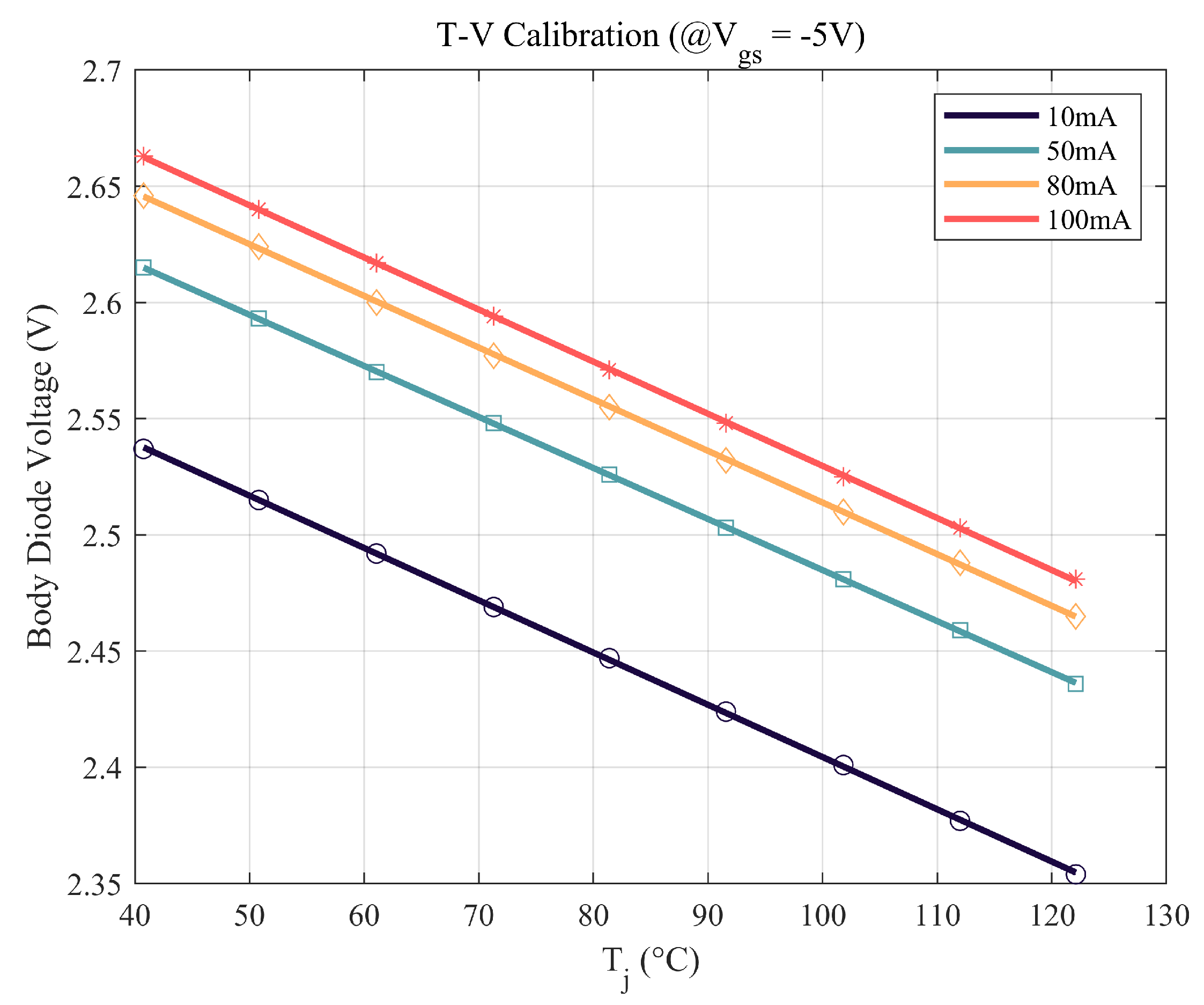
Tests were conducted using small currents of 10 mA, 50 mA, 80 mA, and 100 mA. Ensuring the MOSFET remained in a fully off state during measurements was paramount, necessitating the maintenance of a gate-source voltage of −5 V, as stipulated in the device’s datasheet. This voltage level ensured the complete shutdown of the MOSFET’s forward conduction channel, thereby eliminating any influence from the forward conduction resistance when measuring the voltage across the drain and source terminals. The outcomes are depicted in Figure 6, demonstrating excellent linearity across all four measured currents. Given the laboratory equipment conditions, 100 mA was selected as the sense current for this experiment.
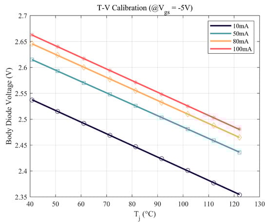
Figure 6.
Calibration curves at different sense currents.
3.2. Power Cycling Test
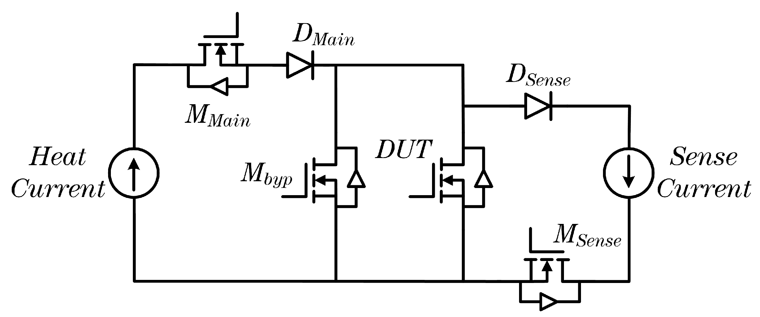
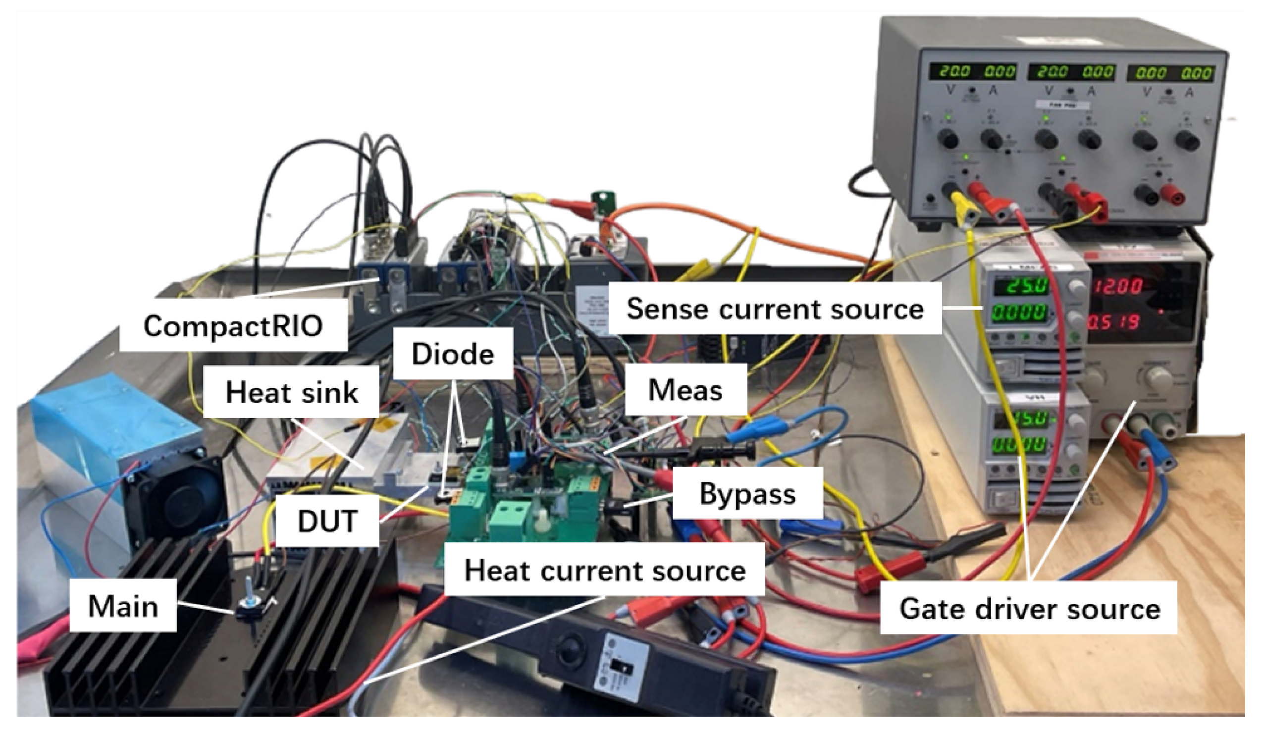
The PCT was conducted in the forward MOSFET mode, involving the passage of a constant current to generate heat within the device. The circuitry for the PCT is depicted in Figure 7, while the test bed is schematically illustrated in Figure 8. The cycling conditions are summarized in Table 5.
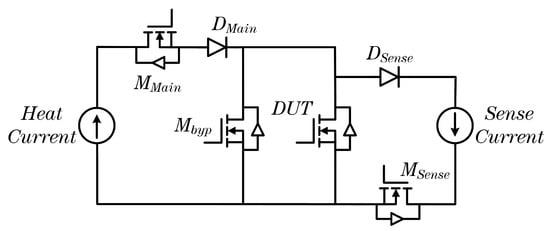
Figure 7.
Circuit diagram of forward-mode power cycling test.

Figure 8.
Illustration of the test bed.
Table 5.
Conditions of the power cycling test.
3.3. Switching Sequence Test
Reference [54] indicated that the device may encounter voltage spikes and extended transient effects during switching state transitions. When measuring the maximum junction temperature, it was observed that the junction temperature experienced a significant drop in a brief period at the commencement of device turn-off. Consequently, the accurate and prompt capture of the voltage value at the instant of device turn-off was paramount for accurate maximum junction temperature measurement. To tackle this challenge, we conducted an investigation into the circuit switching sequence during the device’s turn-off process.
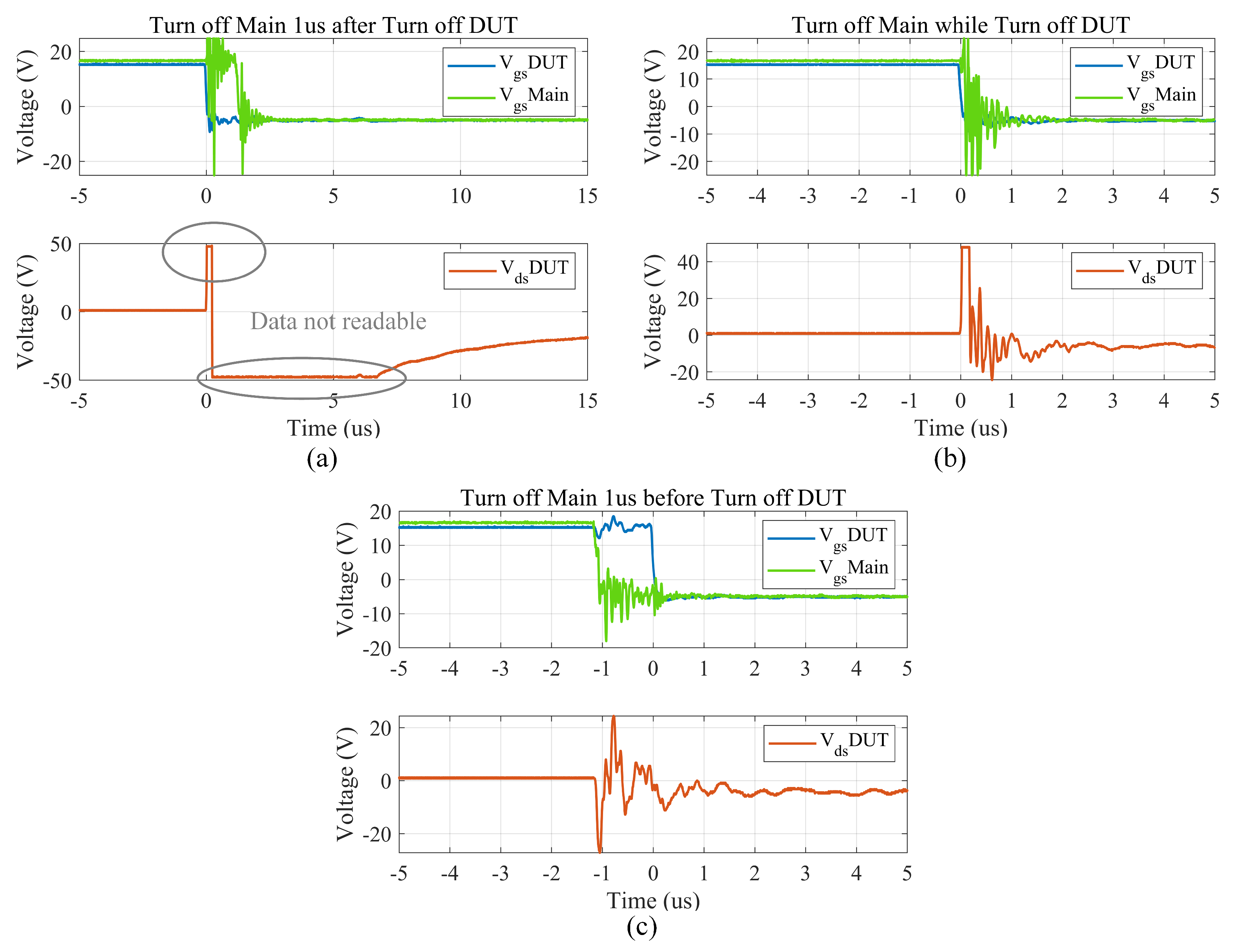
The deactivation sequence during turn-off encompassed the shutdown of both the device under test (DUT) and the Main power source. Figure 9 depicts the traced and measured voltage fluctuations across various sequences. Preceding the deactivation of the Main, turning off the DUT led to a notable voltage spike exceeding 50 V, accompanied by a transient response spanning over 15 s. Alternatively, if both were deactivated concurrently or the Main was deactivated initially, the transient duration was reduced to approximately 3 s. However, the former sequences still induced a voltage spike exceeding 40 V. Therefore, during the experimental setup, it was determined to deactivate the Main initially, followed by the DUT after a brief delay of 1 s.
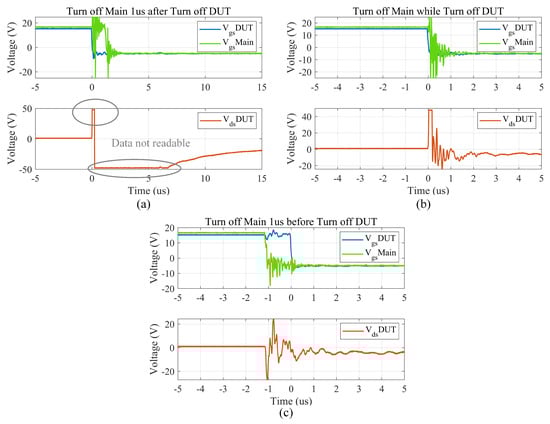
Figure 9.
Experimental comparison of different switching-off sequences to assess their impact on body diode voltage measurements for calculating the maximum junction temperature. (a) Turn off Main first, then turn off DUT. (b) Turn off Main and simultaneously turn off DUT. (c) Turn off DUT first, then turn off Main.
3.4. Threshold Voltage Measurement
According to the datasheet for the C2M0080120D [68] shown in Table 4, the threshold voltage is defined as the gate-source voltage when the gate and drain are short-circuited with a gate-source current of 5 mA flowing.
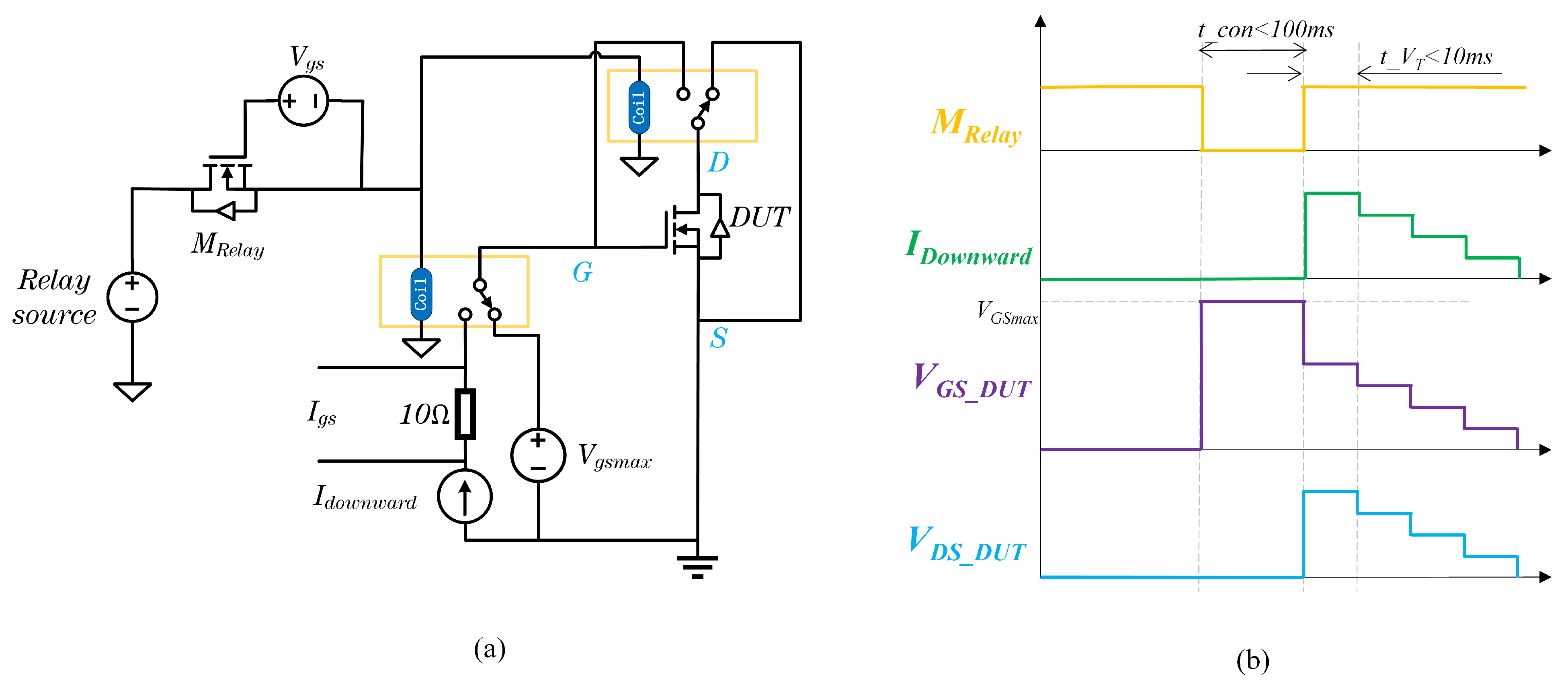
Guided by the threshold voltage measurement conditions outlined in the datasheet, a measurement circuit was devised, as depicted in Figure 10. During experimentation, it was noticed that, despite maintaining a constant measuring current, the threshold voltage gradually rose with increasing dwell time, exhibiting a fluctuation amplitude of up to 0.1 V, as shown in Figure 11. This voltage instability arises from transient effects caused by point defects at the semiconductor–electrode interface in SiC MOSFETs [19], thus posing challenges in accurately determining the threshold voltage during measurement.
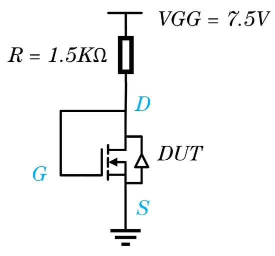
Figure 10.
Threshold voltage measurement circuit 1 based on the datasheet [68]. The gate and drain were shorted before measurement with a 7.5 V voltage applied. A 1.5 k resistor limits the current to 5 mA.
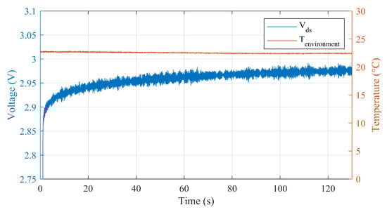
Figure 11.
The results of threshold voltage measurement circuit 1. With the VGG and temperature held relatively constant, the drain-to-source voltage decreased by approximately 0.1 V over time.
Moreover, owing to their wide bandgap characteristics, SiC materials cause notable shifts in the Fermi level’s position during upward voltage scans, necessitating a prolonged period to attain thermal equilibrium. Conversely, during downward voltage scans, the alterations in the Fermi level are minimal, resulting in a nearly instantaneous restoration of thermal equilibrium. This asymmetry introduces a drift in the measured threshold voltage values in both measurement techniques. Notably, the threshold voltage is more precisely determined during the downward scan voltage due to reduced drift, as reported in [19].
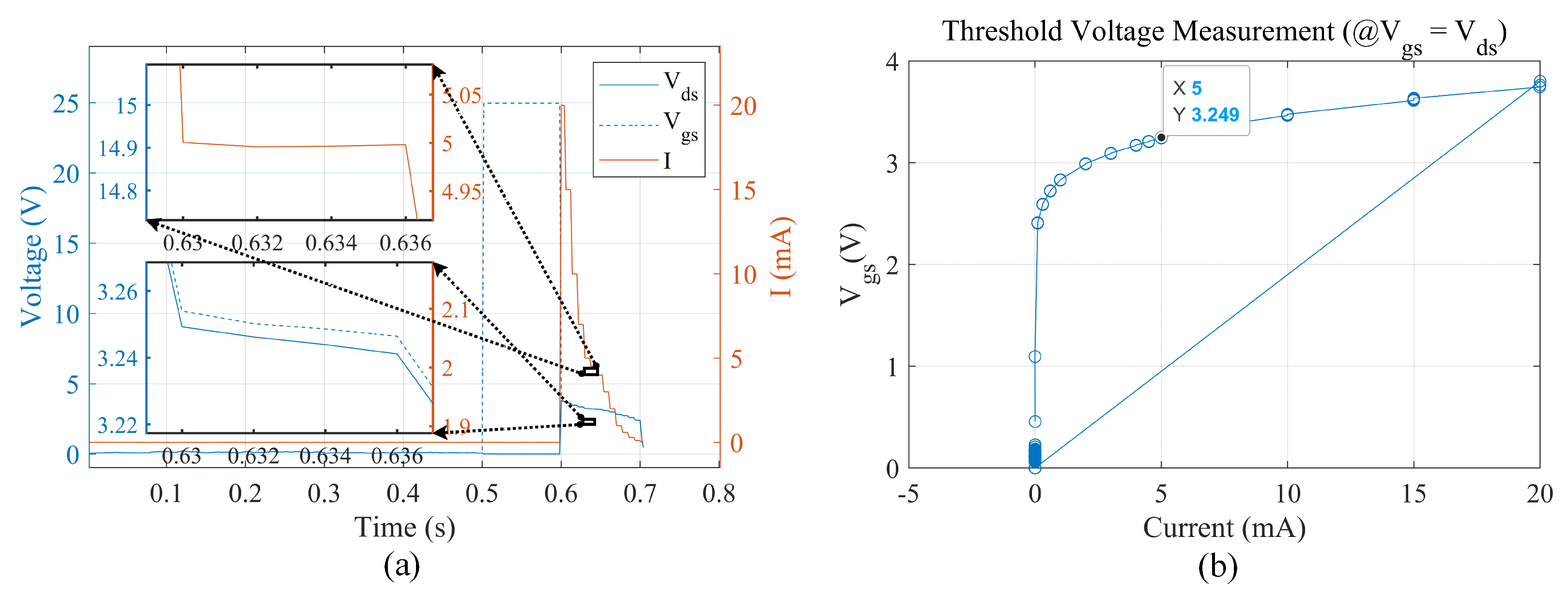
Accordingly, the threshold voltage measurement circuit was set based on standard JEP183A and JEP184 [69,70]. The circuit and timing diagrams are shown in Figure 12. The results are illustrated in Figure 13, where it can be observed that the device voltage decreased slightly at a constant current of around 10 mV, indicating that this approach can greatly improve the effects of the trap near the gate. However, with the second circuit, the duration was short and controllable, enabling the determination of the threshold voltage at a current of 5 mA.
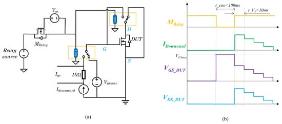
Figure 12.
Threshold voltage measurement circuit 2 set according to JEP183A specifications [69]. (a) Circuit diagram. (b) Timing diagram. Prior to measurement, the drain and source are shorted, and the maximum gate voltage (25 V for this device) is applied. During measurement, the gate and source are quickly disconnected and shorted with a drain while gradually reducing the current. The threshold voltage measurement is taken when the current reaches 5 mA. is used to control relay switching.
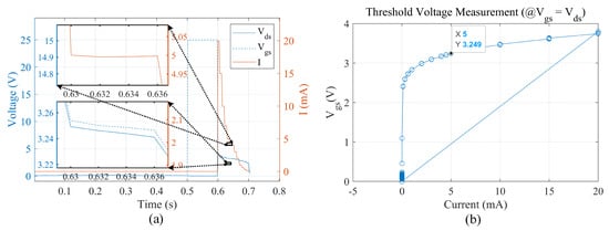
Figure 13.
Timing diagram of threshold voltage measurement circuit 2. (a) Results of voltage and current variation with time. DUT’s is initially set to the maximum value of 25 V, and during measurement, it quickly becomes equal to . The current starts decreasing gradually from 20 mA. In the zoomed-in area, it can be observed that the voltage variation remains around 0.01 V, while the circuit remains essentially unchanged. (b) Corresponding values for different currents.
In the device’s datasheet [68], the threshold voltage of the device at room temperature is approximately 3.25 V. The experimental results, depicted in Figure 13, indicate a threshold voltage of 3.249 V, which aligns well with this specified value.
3.5. Thermal Impedance Measurement
When utilizing the body diode voltage drop under low current as an indicator of the junction temperature, it is feasible to measure the junction temperature solely during the cooling phase. Consequently, we measured the thermal impedance curve of the device corresponding to its cooling curve.
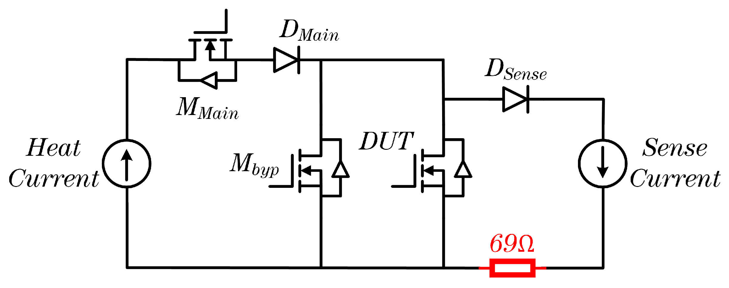
To mitigate the current delay resulting from the power supply mode switch, a 69 resistor was integrated in series with the measurement circuit. The circuit configuration is depicted in Figure 14.

Figure 14.
Thermal characterization measurement circuit. A 69 resistor is substituted for to mitigate current and voltage fluctuations induced by power switching.
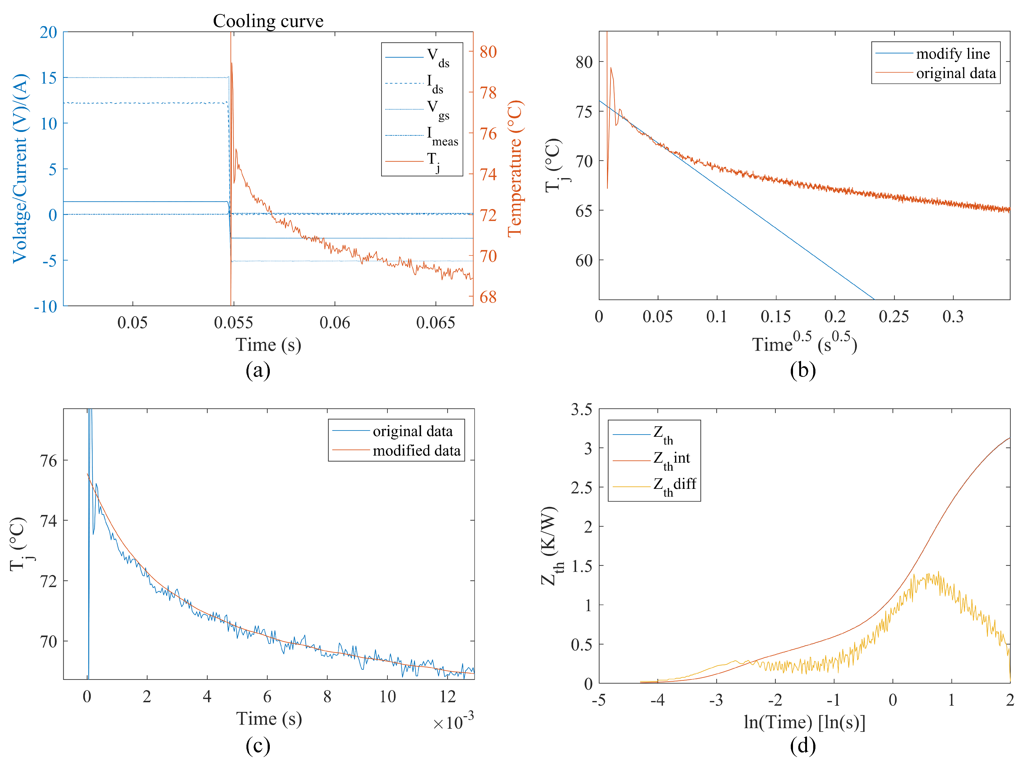
After reaching a thermal equilibrium state, data were recorded for 50 ms during the heating phase to compute the heating power. Subsequently, the cooling phase commenced, and data were recorded for 100 s throughout the cooling process. By this time, the device had cooled nearly to room temperature. Consequently, the cooling curve obtained from the measurements, following appropriate data processing, delineates the thermal impedance curve between the device junction and the surrounding environment. The results are illustrated in Figure 15 ( denotes the result after interpolation, and represents the result after differentiation).
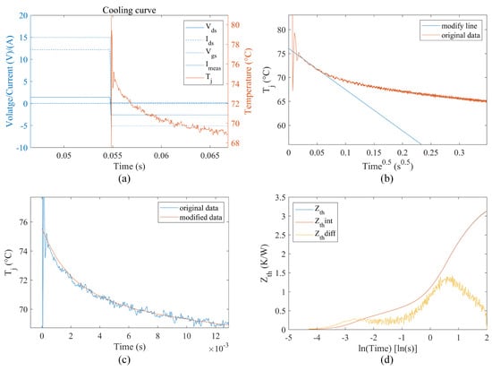
Figure 15.
Thermal impedance calculation process. (a) There is approximately a 40 s fluctuation in the initial switching off. (b) The initial temperature drops linearly with the square root of time. (c) The modified data follow a trend consistent with the original data. (d) Calculated thermal impedance according to Equations (1) and (2).
The initial step in calculating the thermal impedance curve involves converting the cooling curve into the heating curve using Equation (1). Subsequently, the thermal impedance curve is derived by applying Equation (2).
represents the maximum junction temperature of the device in thermal equilibrium under this heating power, while denotes the junction temperature of the device after 100 s of cooling, approaching room temperature. stands for the power passing through the DUT during heating, represents the on-state voltage across the DUT during heating, and denotes the on-state current flowing through the DUT during heating.
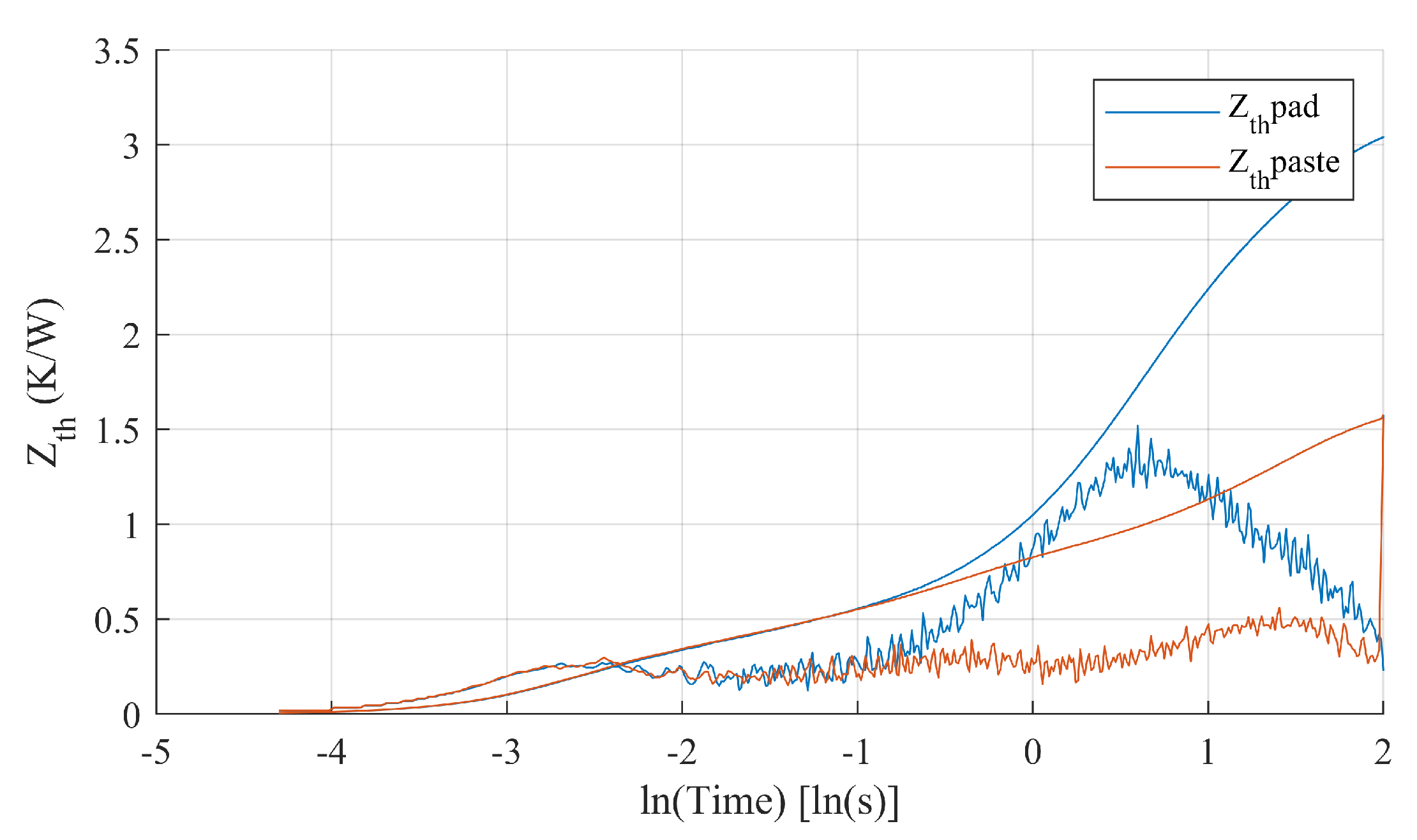
To precisely measure the thermal impedance curve between the device junction and the case, the TDIM method, as outlined in JESD51-14 [20], was utilized. In the initial measurement, a layer of thermal paste was applied between the device and the heatsink, while in the subsequent measurement, a thermal pad was inserted between them. The significant variance in thermal resistance between the thermal paste and the thermal pad caused the cooling curves to diverge at a specific point along the thermal path, indicating the location of the device case. The experimental findings, particularly the curves preceding 0.1 s, are depicted in Figure 16, offering insights into the thermal impedance curve from the device junction to the case.
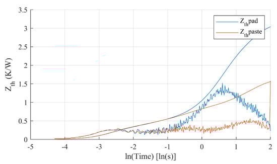
Figure 16.
Measurement of junction-to-case thermal impedance using the TDIM method. The red line represents the measurement result with a layer of paste added between the device and the heatsink, while the blue line represents the measurement result with a thermal pad added.
4. Results and Discussion
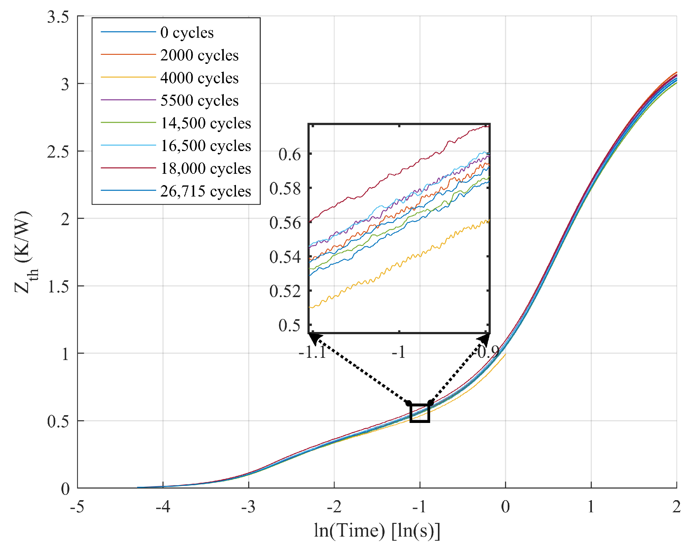
The thermal impedance curve of the device during the PCT is presented in Figure 17, where the measured data for the initial 0.1 s represent the junction-to-case thermal impedance curve. The experimental results indicate that the thermal impedance did not exhibit a distinct or consistent increasing or decreasing trend, exhibiting fluctuations ranging from +4.7% to −5.6%. These fluctuations in the data can be attributed to inherent measurement errors in the instrumentation and variations in ambient temperature. Consequently, it can be deduced that there was no significant degradation of the solder layer within the device.
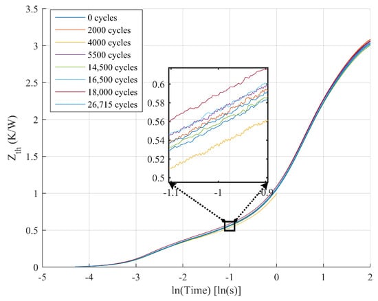
Figure 17.
Fluctuations in thermal impedance curve for DUT1 over the course of a power cycling test.
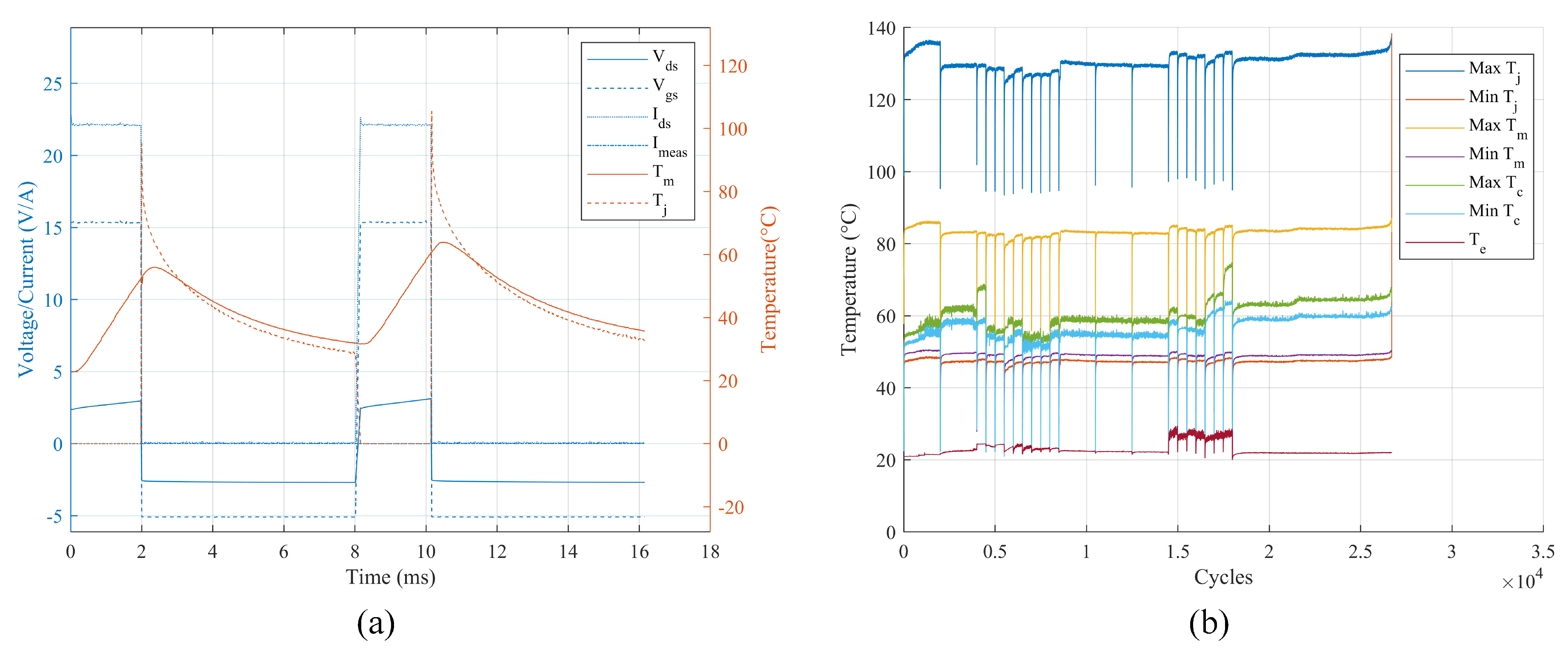
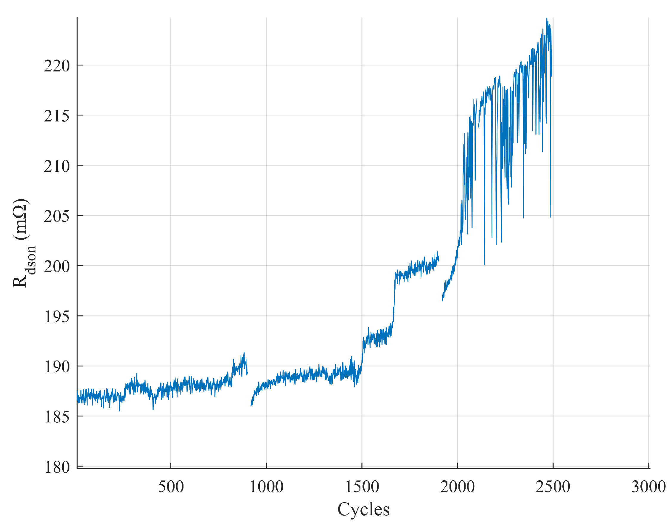
As depicted in Figure 18, after completing the initial 2000 cycles, the device was removed from the test bench, resulting in a change in the contact resistance between the device and the test bench, thereby causing a variation in the maximum . Subsequently, the maximum stayed at around 130 ∘C for the initial 21,000 cycles, exhibiting a slightly increasing trend, as shown in Table 6. Figure 18 indicates that the environmental temperature also influenced the maximum . At around 21,650 cycles, there was a significant rise in the maximum . A distinct and abrupt increase in the maximum was observed during power cycling at around 26,500 cycles. Utilizing the maximum temperature of the 3200th cycle as the baseline value, the percentage variation corresponding to the maximum for different cycles is detailed in Table 6. The results of , a parameter characterizing bond-wire failure, are illustrated in Figure 19, with the associated cycle numbers and percentage increases shown in Table 6. demonstrates a high degree of correlation with the trend of maximum .
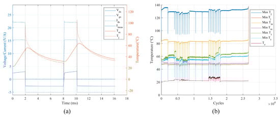
Figure 18.
(a) Temperature, current, and current of DUT1 over time for the first two cycles. (b) Temperature log over the course of a power cycling test. is the junction temperature, is the middle pin temperature, is the case temperature, and is the environmental temperature.
Table 6.
Maximum junction temperature and on-state voltage and resistance of DUT1 over the course of a power cycling test.
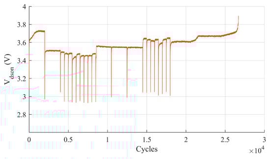
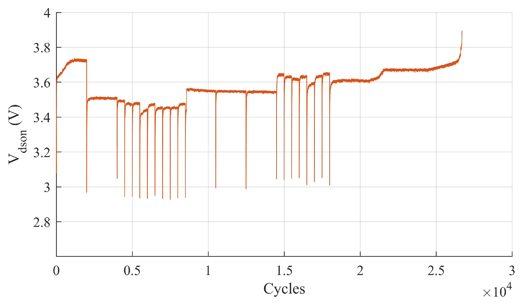
Figure 19.
Log of maximum on-state voltage of DUT1 over the course of a power cycling test.
To mitigate the influence of current fluctuations, the corresponding for different cycles was calculated. However, since exhibited a positive correlation with , it was necessary to consider the impact of fluctuations on . As the TSEP utilized was the body diode voltage drop at small currents, determining during the high-current heating phase, i.e., the on-state phase of the device, was impractical. However, could be reliably measured by affixing a thermocouple at the middle pin of the device, and during the PCT was notably more discernible compared to the case temperature, as depicted in Figure 18. Hence, was regarded as representative of during the heating phase. Given that the thermal impedance of the device remained relatively stable, the relationship between and theoretically remained consistent. The correlation between and during the cooling process was plotted for varying cycle numbers, and the outcomes are illustrated in Figure 20.
Figure 20.
The relationship between the middle pin temperature and junction temperature of DUT1 during the PCT process.
The relationship between and exhibits non-linearity as nears its peak value following cycle stabilization across various cycle counts. Nevertheless, within the temperature range of 50 ∘C to 75 ∘C, a distinct linear correlation is evident, with a maximum error margin of less than 1 ∘C. This correlation is expressed by Equation (3).
was plotted against at 70 °C for each cycle, as depicted in Figure 21. The corresponding measurements for each cycle, along with their percentage increases, are summarized in Table 6. A more consistent increasing trend can be observed from the data. The 5 m to 6 m drop in produced after the 2000 cycle can be attributed to changes in contact resistance within the circuit.
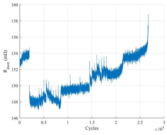
Figure 21.
Log of on-state resistance of DUT1 at a middle pin temperature of 70 °C and a current of 22 A over the course of a power cycling test.
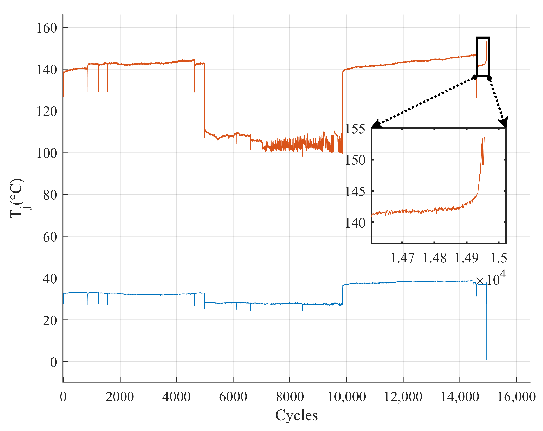
Since there was no significant degradation in the solder layer of the device, the change in primarily stemmed from the failure of the bond wires. The C2M0080120D device with multiple bond wires shown in Figure 18b was compared to the SCT30N120 device with a single bond wire, as shown in Figure 22 (the notch in the PCT from 5000 to 9800 cycles is the maximum change due to the current reduction caused by the misoperation of the current source). It was observed that the sudden change phenomenon occurred only once for the device with a single bond wire, and the device could no longer operate for switching after 20 cycles following the sudden change in . Therefore, it was concluded that one of the bond wires of the C2M0080120D device was lifted at 21,650 cycles, and the other bond wire exhibited visible cracking at 26,500 cycles, during which time the device could continue to operate.

Figure 22.
The variation in maximum and minimum junction temperatures of the single bond-wire device of DUT3 over the course of a power cycling test.
The subsequent operation of another device of the same type after generating a drop of more than 5% in is illustrated in Figure 23. Following the lifting of one bond wire, the of the device increased, resulting in higher power loss at the same current level. This increased power loss led to elevated currents passing through the remaining bond wires, intensifying the thermal stresses on the wires and accelerating the lifting of the other bond wire. The 5% failure criterion typically occurred between the lifting of the first bond wire and the lifting of the other bond wire. Remarkably, the device retained its operational capability during this process. In contrast to a single bond wire, which rapidly lost its functionality, multiple bond wires could still function for a certain period after reaching the failure criterion, thereby potentially enhancing the device’s reliability.
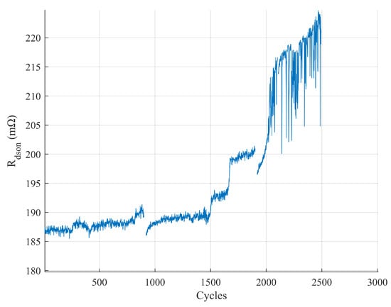
Figure 23.
Subsequent changes in on-state resistance of DUT2 after it increased by more than 5% at a middle pin temperature of 70 ∘C and a current of 25 A.
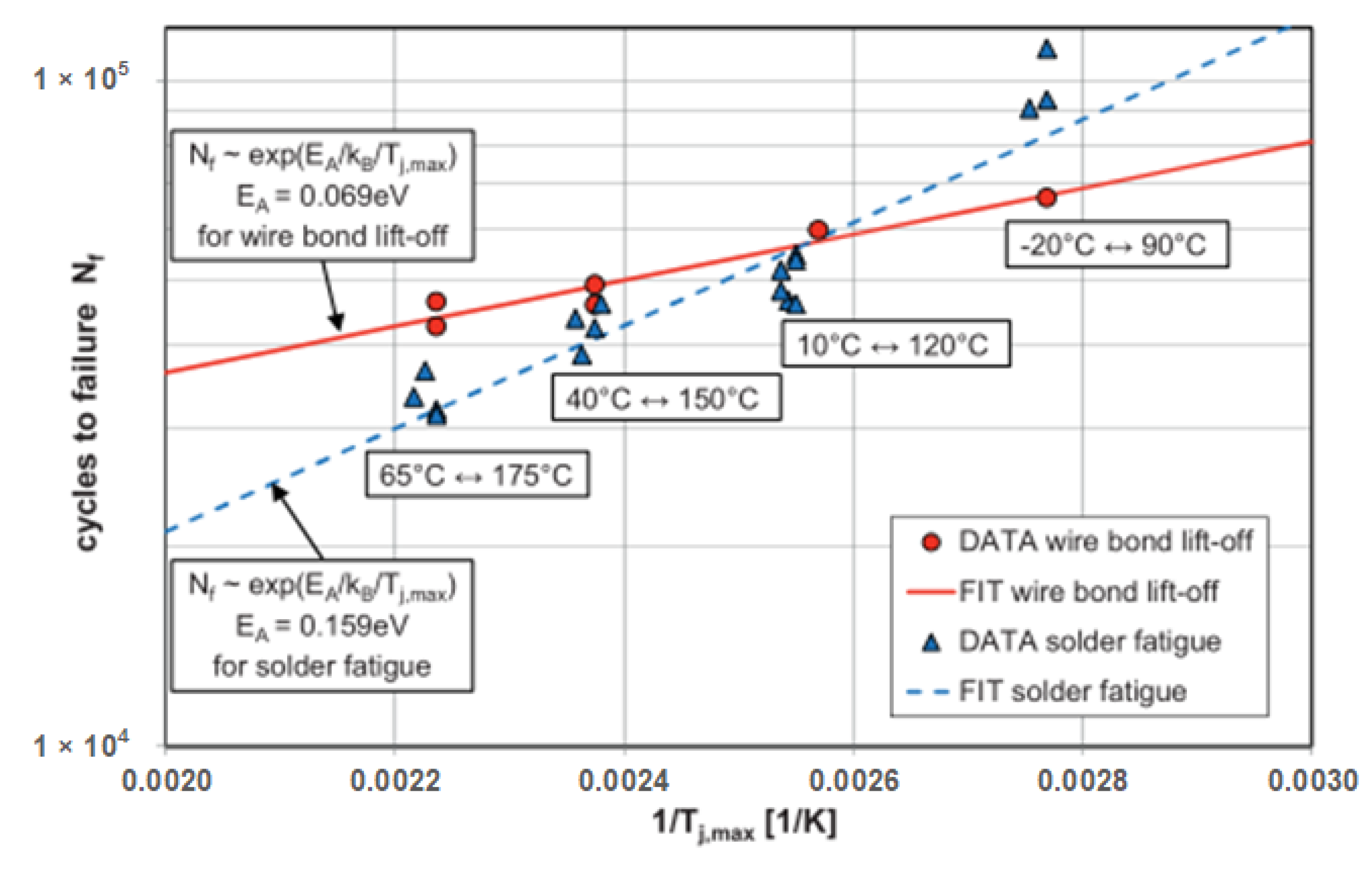
As shown in Figure 17 and Figure 21, the experimental results indicate that under second-level power cycling with fluctuations ranging from approximately 47 ∘C to 130 ∘C, the predominant failures in devices were bond-wire failures, while there was no notable failure observed in the solder layer. The relationship between the number of cycle failures () and the maximum can be expressed as follows: , where represents the activation energy and denotes the Boltzmann constant. Compared to bond wires, solder layer fatigue necessitates higher activation energy, approximately twice the activation energy required for bond wires [71], as illustrated in Figure 24. Under the experimental conditions, where the maximum was slightly lower, the number of cycles needed for solder layer failure exceeded that required for bond wires, thus rendering bond wires more susceptible to failure.
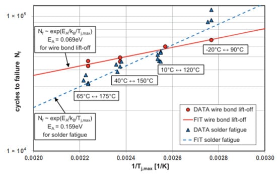
Figure 24.
Impact of maximum junction temperature on solder fatigue and Al bond-wire degradation [56].
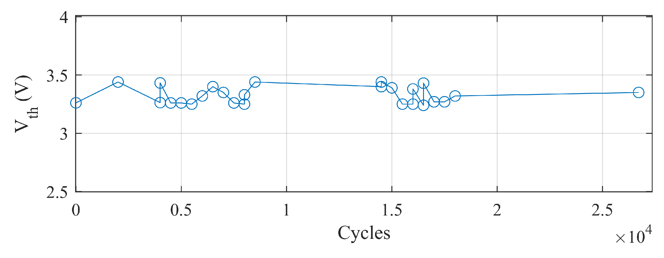
Figure 25 illustrates the fluctuation in the device’s threshold voltage throughout the entire power cycling process. Notably, during the experiment, the threshold voltage exhibited minimal changes, with a fluctuation range of 0.2 V. Given the power cycling test conditions, which involved a positively biased gate voltage of +15 V for 2 s during turn-on and a negatively biased gate voltage of −5 V for 6 s during turn-off, the products of the duration and value for both positively and negatively biased voltages were equivalent. This arrangement mitigates, to some extent, the threshold voltage drift caused by prolonged positive/negative biasing, as reported in [29]. Furthermore, the existing literature [72] indicates that the threshold voltage remains relatively stable when the gate voltage alternates between positive and negative values. This could explain the limited degradation observed in the threshold voltage. According to [19], an increase in the threshold voltage due to drift would typically lead to an increase in channel resistance. However, when comparing the fluctuations in the threshold voltage and resistance, no corresponding decrease in was observed despite an increase in the threshold voltage. Based on our experimental results, a clear correlation between these two parameters does not seem to exist.

Figure 25.
Fluctuation in threshold voltage of DUT1 over the course of a power cycling test.
5. Conclusions
This paper delved into a comprehensive analysis of the forward power cycling behavior of SiC MOSFETs, particularly focusing on temperature fluctuations ranging from 47 ∘C to 130 ∘C. During the experimental process, meticulous attention was paid to eliminating real-time monitoring errors that could arise from the switching sequence, while effectively minimizing errors attributed to short-term threshold voltage drift. Real-time tracking of temperature and resistance parameters was meticulously conducted throughout the experiment, with threshold voltage and thermal impedance measurements taken at specific intervals. The findings revealed a significant increase in both the temperature and on-state resistance with aging. Based on these rigorous experiments, the following conclusions are drawn:
- Bond wires in discrete devices are more susceptible to failure compared to solder layers and chips. For this type of operating environment, it is possible to consider optimizing the bonding wire-to-chip connection to improve the reliability of the device. One possible optimization strategy is to use multiple bond wires and increase the strength of the bond wire-to-chip connection. Such an improvement is expected to significantly enhance the performance and lifetime of the device.
- In this paper, we discussed that using an offline approach to threshold voltage measurement can largely attenuate the short-term drift of a single threshold voltage measurement. However, there was still a 0.2 V fluctuation in the threshold voltage during the PCT. At the same time, we found that there was an inconsistency between the drift of the threshold voltage and the change in the on-state resistance. In subsequent experiments, we intend to expand the number of research devices to further investigate the threshold voltage measurement and its relationship with on-state resistance in depth.
Author Contributions
Conceptualization, T.H., B.P.S. and S.N.; methodology, T.H. and B.P.S.; software, T.H. and B.P.S.; validation, T.H.; formal analysis, T.H.; investigation, T.H.; resources, B.P.S.; data curation and writing—original draft preparation, T.H.; writing—review and editing, B.P.S., S.N. and Y.L.; visualization, T.H.; supervision, S.N. and Y.L.; project administration, T.H.; funding acquisition, S.N. and Y.L. All authors have read and agreed to the published version of the manuscript.
Funding
This research was supported by the China Scholarship Council (CSC).
Data Availability Statement
Data are contained within the article.
Acknowledgments
This work was supported by the Swedish Electromobility Center (SEC) and KTH Royal Institute of Technology.
Conflicts of Interest
The funders had no role in the design of the study; in the collection, analyses, or interpretation of data; in the writing of the manuscript; or in the decision to publish the results.
Abbreviations
| CTE | coefficients of thermal expansion |
| DUT | device under test |
| IGBT | insulated-gate bipolar transistor |
| MOSFET | metal–oxide–semiconductor field-effect transistor |
| PCT | power cycling test |
| TDIM | transient dual-interface measurement |
| TSEP | temperature-sensitive electrical parameter |
| Si | silicon |
| SiC | silicon carbide |
References
- Alharbi, S.S.; Alharbi, S.S.; Matin, M. An Improved Interleaved DC-DC SEPIC Converter Based on SiC-Cascade Power Devices for Renewable Energy Applications. In Proceedings of the 2018 IEEE International Conference on Electro/Information Technology (EIT), Rochester, MI, USA, 3–5 May 2018; pp. 0487–0492. [Google Scholar] [CrossRef]
- Yan, J.; Zhang, H.; Liu, Y.; Han, S.; Li, L.; Lu, Z. Forecasting the High Penetration of Wind Power on Multiple Scales Using Multi-to-Multi Mapping. IEEE Trans. Power Syst. 2018, 33, 3276–3284. [Google Scholar] [CrossRef]
- Chaudhary, O.S.; Denaï, M.; Refaat, S.S.; Pissanidis, G. Technology and Applications of Wide Bandgap Semiconductor Materials: Current State and Future Trends. Energies 2023, 16, 6689. [Google Scholar] [CrossRef]
- Johannesson, D.; Nawaz, M.; Norrga, S.; Nee, H.P. Evaluation of Ultrahigh-Voltage 4H-SiC Gate Turn-OFF Thyristors and Insulated-Gate Bipolar Transistors for High-Power Applications. IEEE Trans. Power Electron. 2022, 37, 4133–4147. [Google Scholar] [CrossRef]
- Peyghami, S.; Palensky, P.; Blaabjerg, F. An Overview on the Reliability of Modern Power Electronic Based Power Systems. IEEE Open J. Power Electron. 2020, 1, 34–50. [Google Scholar] [CrossRef]
- Xu, S.; Xue, Y.; Chang, L. Review of Power System Support Functions for Inverter-Based Distributed Energy Resources- Standards, Control Algorithms, and Trends. IEEE Open J. Power Electron. 2021, 2, 88–105. [Google Scholar] [CrossRef]
- Elasser, A.; Chow, T. Silicon Carbide Benefits and Advantages for Power Electronics Circuits and Systems. Proc. IEEE 2002, 90, 969–986. [Google Scholar] [CrossRef]
- Bhakare, O.; Ghosh, K.; Chakraborty, S.S.; Hatua, K. Experimental Study and Comparison of Switching Loss Behavior of Si IGBT and SiC MOSFET in Dual Active Bridge Series Resonant Converter. In Proceedings of the2023 IEEE International Conference on Environment and Electrical Engineering and 2023 IEEE Industrial and Commercial Power Systems Europe (EEEIC/I&CPS Europe), Madrid, Spain, 6–9 June 2023; pp. 1–6. [Google Scholar] [CrossRef]
- Matocha, K.; Losee, P.; Glaser, J.; Nasadoski, J.; Arthur, S.; Stevanovic, L. Getting the Most from SiC MOSFETs: Optimizing Conduction and Switching Losses for High Performance Power Electronics Applications. In Proceedings of the 2009 International Semiconductor Device Research Symposium ISDRS, College Park, MD, USA, 9–11 December 2009; pp. 1–2. [Google Scholar] [CrossRef]
- What Are SiC Semiconductors? SiC | Electronics Basics | ROHM. Available online: https://www.rohm.com/electronics-basics/sic/what-are-sic-semiconductors (accessed on 23 March 2024).
- Wang, J.; Shuai, Z.; Shen, J. Feasibility of High Voltage SiC Thyristor in HVDC Transmission. In Proceedings of the 2014 IEEE PES Asia-Pacific Power and Energy Engineering Conference (APPEEC), Hong Kong, China, 7–10 December 2014; pp. 1–4. [Google Scholar] [CrossRef]
- Yuan, X.; Wang, J.; Laird, I.; Zhou, W. Wide-Bandgap Device Enabled Multilevel Converters with Simplified Structures and Capacitor Voltage Balancing Capability. IEEE Open J. Power Electron. 2021, 2, 414–423. [Google Scholar] [CrossRef]
- Heinig, S.; Jacobs, K.; Ilves, K.; Norrga, S.; Nee, H.P. Auxiliary Power Supplies for High-Power Converter Submodules: State of the Art and Future Prospects. IEEE Trans. Power Electron. 2022, 37, 6807–6820. [Google Scholar] [CrossRef]
- Wang, Z.; Shi, X.; Tolbert, L.M.; Wang, F.; Liang, Z.; Costinett, D.; Blalock, B.J. A high temperature silicon carbide mosfet power module with integrated silicon-on-insulator-based gate drive. IEEE Trans. Power Electron. 2015, 30, 1432–1445. [Google Scholar] [CrossRef]
- Rabkowski, J.; Peftitsis, D.; Nee, H.P. Silicon Carbide Power Transistors: A New Era in Power Electronics Is Initiated. IEEE Ind. Electron. Mag. 2012, 6, 17–26. [Google Scholar] [CrossRef]
- Ugur, E.; Yang, F.; Pu, S.; Zhao, S.; Akin, B. Degradation Assessment and Precursor Identification for SiC MOSFETs under High Temp Cycling. IEEE Trans. Ind. Appl. 2019, 55, 2858–2867. [Google Scholar] [CrossRef]
- Vellukunnel, M.T.; Khanal, M.; Fan, X. Thermal Stresses in a Bi-Layer Assembly in Electronics Packaging. In Proceedings of the 2023 24th International Conference on Thermal, Mechanical and Multi-Physics Simulation and Experiments in Microelectronics and Microsystems (EuroSimE), Graz, Austria, 16–19 April 2023; pp. 1–7. [Google Scholar] [CrossRef]
- Choi, U.M.; Blaabjerg, F.; Jørgensen, S. Power Cycling Test Methods for Reliability Assessment of Power Device Modules in Respect to Temperature Stress. IEEE Trans. Power Electron. 2018, 33, 2531–2551. [Google Scholar] [CrossRef]
- Aichinger, T.; Rescher, G.; Pobegen, G. Threshold Voltage Peculiarities and Bias Temperature Instabilities of SiC MOSFETs. Microelectron. Reliab. 2018, 80, 68–78. [Google Scholar] [CrossRef]
- JESD51-14; Transient Dual Interface Test Method for the Measurement of the Thermal Resistance Junction to Case of Semiconductor Devices with Heat Flow Trough a Single Path. JEDEC: Arlington County, VA, USA, 2010.
- Wang, Y.; Ding, Y.; Yin, Y. Reliability of Wide Band Gap Power Electronic Semiconductor and Packaging: A Review. Energies 2022, 15, 6670. [Google Scholar] [CrossRef]
- Lelis, A.J.; Green, R.; Habersat, D.B.; El, M. Basic Mechanisms of Threshold-Voltage Instability and Implications for Reliability Testing of SiC MOSFETs. IEEE Trans. Electron Devices 2015, 62, 316–323. [Google Scholar] [CrossRef]
- Gonzalez, J.O.; Wu, R.; Jahdi, S.; Alatise, O. Performance and Reliability Review of 650 V and 900 V Silicon and SiC Devices: MOSFETs, Cascode JFETs and IGBTs. IEEE Trans. Ind. Electron. 2020, 67, 7375–7385. [Google Scholar] [CrossRef]
- Green, R.; Lelis, A.J.; Nouketcha, F.L. Comparison of SiC MOSFET Characteristics Following Body-Diode Forward-Current Stress. Mater. Sci. Forum 2019, 963, 583–587. [Google Scholar] [CrossRef]
- Karki, U.; Peng, F.Z. Effect of Gate-Oxide Degradation on Electrical Parameters of Power MOSFETs. IEEE Trans. Power Electron. 2018, 33, 10764–10773. [Google Scholar] [CrossRef]
- Ye, X.; Chen, C.; Wang, Y.; Zhai, G.; Vachtsevanos, G.J. Online Condition Monitoring of Power MOSFET Gate Oxide Degradation Based on Miller Platform Voltage. IEEE Trans. Power Electron. 2017, 32, 4776–4784. [Google Scholar] [CrossRef]
- Pavlovic, Z.; Manic, I.; Prijic, Z.; Davidovic, V.; Stojadinovic, N. Influence of Gate Oxide Charge Density on VDMOS Transistor ON-resistance. In Proceedings of the 2000 22nd International Conference on Microelectronics. Proceedings (Cat. No.00TH8400), Nis, Serbia, 14–17 May 2000; Volume 2, pp. 663–666. [Google Scholar] [CrossRef]
- Losee, P.; Bolotnikov, A.; Yu, L.; Beaupre, R.; Stum, Z.; Kennerly, S.; Dunne, G.; Sui, Y.; Kretchmer, J.; Johnson, A.; et al. 1.2 kV Class SiC MOSFETs with Improved Performance over Wide Operating Temperature. In Proceedings of the 2014 IEEE 26th International Symposium on Power Semiconductor Devices & IC’s (ISPSD), Waikoloa, HI, USA, 15–19 June 2014; pp. 297–300. [Google Scholar] [CrossRef]
- Chen, J.; Deng, E.; Zhao, Z.; Wu, Y.; Huang, Y. Power Cycling Capability Comparison of Si and SiC MOSFETs under Different Conduction Modes. In Proceedings of the 2020 32nd International Symposium on Power Semiconductor Devices and ICs (ISPSD), Vienna, Austria, 13–18 September 2020; pp. 541–544. [Google Scholar] [CrossRef]
- Nguyen, T.T.; Ahmed, A.; Thang, T.V.; Park, J.H. Gate Oxide Reliability Issues of SiC MOSFETs Under Short-Circuit Operation. IEEE Trans. Power Electron. 2015, 30, 2445–2455. [Google Scholar] [CrossRef]
- Funaki, T. A Study on Performance Degradation of SiC MOSFET for Burn-in Test of Body Diode. In Proceedings of the 2013 4th IEEE International Symposium on Power Electronics for Distributed Generation Systems (PEDG), Rogers, AR, USA, 8–11 July 2013; pp. 1–5. [Google Scholar] [CrossRef]
- Bonyadi, R.; Alatise, O.; Jahdi, S.; Hu, J.; Evans, L.; Mawby, P.A. Investigating the Reliability of SiC MOSFET Body Diodes Using Fourier Series Modelling. In Proceedings of the 2014 IEEE Energy Conversion Congress and Exposition (ECCE), Pittsburgh, PA, USA, 14–18 September 2014; pp. 443–448. [Google Scholar] [CrossRef]
- Agarwal, A.; Fatima, H.; Haney, S.; Ryu, S.H. A New Degradation Mechanism in High-Voltage SiC Power MOSFETs. IEEE Electron. Device Lett. 2007, 28, 587–589. [Google Scholar] [CrossRef]
- Yang, X.; Zhang, Y.; Wu, X.; Liu, G. Failure Mode Classification of IGBT Modules Under Power Cycling Tests Based on Data-Driven Machine Learning Framework. IEEE Trans. Power Electron. 2023, 38, 16130–16141. [Google Scholar] [CrossRef]
- Wang, Y.; Dai, X.; Liu, G.; Wu, Y.; Li, D.; Jones, S. Status and Trend of SiC Power Semiconductor Packaging. In Proceedings of the 2015 16th International Conference on Electronic Packaging Technology (ICEPT), Changsha, China, 11–14 August 2015; pp. 396–402. [Google Scholar] [CrossRef]
- Nguyen, Q.; Roberts, J.C.; Suhling, J.C.; Jaeger, R.C.; Lall, P. A Study on Die Stresses in Flip Chip Package Subjected to Various Hygrothermal Exposures. In Proceedings of the 2018 17th IEEE Intersociety Conference on Thermal and Thermomechanical Phenomena in Electronic Systems (ITherm), San Diego, CA, USA, 29 May–1 June 2018; pp. 1339–1350. [Google Scholar] [CrossRef]
- Luo, H.; Iannuzzo, F.; Baker, N.; Blaabjerg, F.; Li, W.; He, X. Study of Current Density Influence on Bond Wire Degradation Rate in SiC MOSFET Modules. IEEE J. Emerg. Sel. Top. Power Electron. 2020, 8, 1622–1632. [Google Scholar] [CrossRef]
- Yang, K.; Zhou, L.; Wu, F.; Yang, G.; Ding, L.; Li, K.; Li, X. Simulation of crack propagation in solder layer of IGBT device under temperature shock by viscoplastic phase field method. Eng. Fract. Mech. 2023, 284, 109260. [Google Scholar] [CrossRef]
- Chen, J.; Jiang, X.; Li, Z.; Yu, H.; Wang, J.; Shen, Z.J. Investigation on Effects of Thermal Stress on SiC MOSFET Degradation through Power Cycling Tests. In Proceedings of the 2020 IEEE Applied Power Electronics Conference and Exposition (APEC), New Orleans, LA, USA, 15–19 March 2020; pp. 1106–1110. [Google Scholar] [CrossRef]
- Yang, X.; Ye, J.; Wu, X.; Heng, K.; He, Y.; Liu, G. Lifetime Prediction for Lift-off of Bond Wires in IGBTs Using Paris Law with Analytical Calculation of Crack Length. IEEE Trans. Power Electron. 2023, 38, 13099–13110. [Google Scholar] [CrossRef]
- Fu, S.; Mei, Y.; Li, X.; Ma, C.; Lu, G.Q. A Multichip Phase-Leg IGBT Module Bonded by Pressureless Sintering of Nanosilver Paste. IEEE Trans. Device Mater. Reliab. 2017, 17, 146–156. [Google Scholar] [CrossRef]
- Medjahed, H.; Vidal, P.E.; Nogarede, B. Thermo-Mechanical Stress of Bonded Wires Used in High Power Modules with Alternating and Direct Current Modes. Microelectron. Reliab. 2012, 52, 1099–1104. [Google Scholar] [CrossRef]
- Krüger, M.; Trampert, S.; Middendorf, A.; Schmitz, S.; Lang, K.D. Early-State Crack Detection Method for Heel-Cracks in Wire Bond Interconnects. In Proceedings of the 2014 IEEE 64th Electronic Components and Technology Conference (ECTC), Orlando, FL, USA, 27–30 May 2014; pp. 114–118. [Google Scholar] [CrossRef]
- Xie, L.; Deng, E.; Yang, S.; Zhang, Y.; Zhong, Y.; Wang, Y.; Huang, Y. State-of-the-Art of the Bond Wire Failure Mechanism and Power Cycling Lifetime in Power Electronics. Microelectron. Reliab. 2023, 147, 115060. [Google Scholar] [CrossRef]
- Du, M.; Xin, J.; Wang, H.; Ouyang, Z. Aging Diagnosis of Bond Wire Using On-State Drain-Source Voltage Separation for SiC MOSFET. IEEE Trans. Device Mater. Reliab. 2021, 21, 41–47. [Google Scholar] [CrossRef]
- AQG 324; Qualification of Power Modules for Use in Power Electronics Converter Units in Motor Vehicles. ECPE European Center for Power Electronics e.V.: Nuremberg, Germany, 2021.
- Xie, X.; Bi, X.; Li, G. Thermal-Mechanical Fatigue Reliability of Pbsnag Solder Layer of Die Attachment for Power Electronic Devices. In Proceedings of the 2009 International Conference on Electronic Packaging Technology & High Density Packaging, ICEPT-HDP, Beijing, China, 10–13 August 2009; pp. 1181–1185. [Google Scholar] [CrossRef]
- R, E.; Kavithaa, G.; Samavatian, V.; Alhaifi, K.; Kokabi, A.; Moayedi, H. Reliability Enhancement of a Power Semiconductor with Optimized Solder Layer Thickness. IEEE Trans. Power Electron. 2020, 35, 6397–6404. [Google Scholar] [CrossRef]
- Ciappa, M. Selected Failure Mechanisms of Modern Power Modules. Microelectron. Reliab. 2002, 42, 653–667. [Google Scholar] [CrossRef]
- Lai, W.; Chen, M.; Ran, L.; Xu, S.; Jiang, N.; Wang, X.; Alatise, O.; Mawby, P. Experimental Investigation on the Effects of Narrow Junction Temperature Cycles on Die-Attach Solder Layer in an IGBT Module. IEEE Trans. Power Electron. 2017, 32, 1431–1441. [Google Scholar] [CrossRef]
- Ji, B.; Pickert, V.; Cao, W.P.; Xing, L. Onboard Condition Monitoring of Solder Fatigue in IGBT Power Modules. In Proceedings of the 2013 9th IEEE International Symposium on Diagnostics for Electric Machines, Power Electronics and Drives (SDEMPED), Valencia, Spain, 27–30 August 2013; pp. 9–15. [Google Scholar] [CrossRef]
- Di Nuzzo, G.; Tuellmann, M.; Methfessel, T.; Rzepka, S. Condition Monitoring Indicators for Si and SiC Power Modules. Microelectron. Reliab. 2022, 138, 114614. [Google Scholar] [CrossRef]
- Xie, L.; Wu, L.; Deng, E.; Zhang, Y.; Zhao, Y.; Huang, Y. Difference Between the PWM and Standard DC Power Cycling Tests Based on the Finite-Element Simulation. IEEE Trans. Power Electron. 2023, 38, 8880–8893. [Google Scholar] [CrossRef]
- Yang, F.; Ugur, E.; Akin, B. Design Methodology of DC Power Cycling Test Setup for SiC MOSFETs. IEEE J. Emerg. Sel. Top. Power Electron. 2020, 8, 4144–4159. [Google Scholar] [CrossRef]
- Scheuermann, U.; Schuler, S. Power Cycling Results for Different Control Strategies. Microelectron. Reliab. 2010, 50, 1203–1209. [Google Scholar] [CrossRef]
- Scheuermann, U.; Junghaenel, M. Limitation of Power Module Lifetime Derived from Active Power Cycling Tests. In Proceedings of the 10th International Conference on Integrated Power Electronics Systems, Stuttgart, Germany, 20–22 March 2018; pp. 1–10. [Google Scholar]
- Liu, P.; Zhang, X.; Yin, S.; Tu, C.; Huang, S. Simplified Junction Temperature Estimation Using Integrated NTC Sensor for SiC Modules. In Proceedings of the 2018 IEEE International Power Electronics and Application Conference and Exposition (PEAC), Shenzhen, China, 4–7 November 2018; pp. 1–4. [Google Scholar] [CrossRef]
- Morozumi, A.; Yamada, K.; Miyasaka, T.; Sumi, S.; Seki, Y. Reliability of Power Cycling for IGBT Power Semiconductor Modules. IEEE Trans. Ind. Appl. 2003, 39, 665–671. [Google Scholar] [CrossRef]
- Ceccarelli, L.; Kotecha, R.M.; Bahman, A.S.; Iannuzzo, F.; Mantooth, H.A. Mission-Profile-Based Lifetime Prediction for a SiC Mosfet Power Module Using a Multi-Step Condition-Mapping Simulation Strategy. IEEE Trans. Power Electron. 2019, 34, 9698–9708. [Google Scholar] [CrossRef]
- Stella, F.; Pellegrino, G.; Armando, E.; Daprà, D. Online Junction Temperature Estimation of SiC Power MOSFETs through On-State Voltage Mapping. IEEE Trans. Ind. Appl. 2018, 54, 3453–3462. [Google Scholar] [CrossRef]
- Griffo, A.; Wang, J.; Colombage, K.; Kamel, T. Real-Time Measurement of Temperature Sensitive Electrical Parameters in SiC Power MOSFETs. IEEE Trans. Ind. Electron. 2018, 65, 2663–2671. [Google Scholar] [CrossRef]
- Herold, C.; Sun, J.; Seidel, P.; Tinschert, L.; Lutz, J. Power Cycling Methods for SiC MOSFETs. In Proceedings of the 2017 29th International Symposium on Power Semiconductor Devices and IC’s (ISPSD), Sapporo, Japan, 28 May–1 June 2017; pp. 367–370. [Google Scholar] [CrossRef]
- Yang, X.; Xu, S.; Heng, K.; Wu, X. Distributed Thermal Modeling for Power Devices and Modules with Equivalent Heat Flow Path Extraction. IEEE J. Emerg. Sel. Top. Power Electron. 2023, 11, 5863–5876. [Google Scholar] [CrossRef]
- Siegal, B. An Alternative Approach to Junction-to-Case Thermal Resistance Measurements. Electron. Cool. Mag. 2001, 7, 52–57. Available online: https://api.semanticscholar.org/CorpusID:137928863 (accessed on 23 March 2024).
- Szabo, P.; Steffens, O.; Lenz, M.; Farkas, G. Transient Junction-to-Case Thermal Resistance Measurement Methodology of High Accuracy and High Repeatability. IEEE Trans. Compon. Packag. Technol. 2005, 28, 630–636. [Google Scholar] [CrossRef]
- Steffens, O.; Szabo, P.; Lenz, M.; Farkas, G. Thermal Transient Characterization Methodology for Single-Chip and Stacked Structures. In Proceedings of the Semiconductor Thermal Measurement and Management IEEE Twenty First Annual IEEE Symposium, San Jose, CA, USA, 15–17 March 2005; pp. 313–321. [Google Scholar] [CrossRef]
- Schweitzer, D.; Pape, H.; Chen, L. Transient Measurement of the Junction-To-Case Thermal Resistance Using Structure Functions: Chances and Limits. In Proceedings of the 2008 Twenty-fourth Annual IEEE Semiconductor Thermal Measurement and Management Symposium, San Jose, CA, USA, 16–20 March 2008; pp. 191–197. [Google Scholar] [CrossRef]
- C2M0080120D. Wolfspeed: Durham, NC, USA, 2023.
- JEP183A; Guidelines for Measuring the Threshold Voltage (VT) of SiC MOSFETs. JEDEC: Arlington County, VA, USA, 2023.
- JEP184; Guideline for evaluating Bias Temperature Instability of Silicon Carbide Metal-Oxide-Semiconductor Devices for Power Electronic Conversion. JEDEC: Arlington County, VA, USA, 2021.
- Schmidt, R.; Zeyss, F.; Scheuermann, U. Impact of Absolute Junction Temperature on Power Cycling Lifetime. In Proceedings of the 2013 15th European Conference on Power Electronics and Applications (EPE), Lille, France, 2–6 September 2013; pp. 1–10. [Google Scholar] [CrossRef]
- Ouaida, R.; Berthou, M.; León, J.; Perpiñà, X.; Oge, S.; Brosselard, P.; Joubert, C. Gate Oxide Degradation of SiC MOSFET in Switching Conditions. IEEE Electron. Device Lett. 2014, 35, 1284–1286. [Google Scholar] [CrossRef]


Disclaimer/Publisher’s Note: The statements, opinions and data contained in all publications are solely those of the individual author(s) and contributor(s) and not of MDPI and/or the editor(s). MDPI and/or the editor(s) disclaim responsibility for any injury to people or property resulting from any ideas, methods, instructions or products referred to in the content. |
© 2024 by the authors. Licensee MDPI, Basel, Switzerland. This article is an open access article distributed under the terms and conditions of the Creative Commons Attribution (CC BY) license (https://creativecommons.org/licenses/by/4.0/).