Article

Dual-Module Ultrawide Dynamic-Range High-Power Rectifier for WPT Systems

by
Xiaochen Yu
1,2,
Jinyao Zhang
1,
Minzhang Liu
1,
Xiantao Yang
1,
Yi Huang
1,
Ta-Jen Yen
3 and
Jiafeng Zhou
1,*
1
Department of Electrical Engineering and Electronics, University of Liverpool, Liverpool L69 3GJ, UK
2
International Intercollegiate Ph.D. Program, National Tsing Hua University, Hsinchu 300044, Taiwan
3
Department of Materials Science and Engineering, National Tsing Hua University, Hsinchu 300044, Taiwan
*
Author to whom correspondence should be addressed.
Energies 2024, 17(11), 2707; https://doi.org/10.3390/en17112707
Submission received: 5 May 2024 / Revised: 17 May 2024 / Accepted: 30 May 2024 / Published: 3 June 2024

Abstract

:
Rectifier plays a pivotal role in wireless power transfer systems. While numerous studies have concentrated on enhancing efficiency and bandwidth at specific high-power levels, practical scenarios often involve unpredictable power inputs. Consequently, a distinct need arises for a rectifier that demonstrates superior efficiency across a broad range of input power levels. This paper introduces a high-power RF-to-DC rectifier designed for WPT applications, featuring an ultrawide dynamic range of input power. The rectification process leverages a GaN (gallium nitride) high electron mobility transistor (HEMT) to efficiently handle high power levels up to 12.6 W. The matching circuit was designed to ensure that the rectifier will operate in class-F mode. A Schottky diode is incorporated into the design for relatively lower-power rectification. Seamless switching between the rectification modes of the two circuits is accomplished through the integration of a circulator. The proposed rectifier exhibits a 27.5 dB dynamic range, achieving an efficiency exceeding 55% at 2.4 GHz. Substantial improvement in power handling and dynamic range over traditional rectifiers is demonstrated.

1. Introduction

Wireless power transfer (WPT) represents a non-contact method of delivering energy through the air, eliminating the need for traditional current-carrying cords. The prominence of WPT has surged due to its flexibility; safety features; and diverse applications across various fields, including electric vehicles [1,2,3], implantable medical devices [4,5,6,7], and the charging of portable electronic devices [8,9,10].
A typical radio frequency (RF) WPT system structure (Figure 1) comprises a transmitting antenna and a rectenna system with the following three essential components: a receiving antenna, a impedance-matching network circuit, and a rectifier circuit. At the receiving end of a microwave WPT system, the antenna captures radiated RF signals from a transmission station, converting them into alternating current (AC) voltage. The matching circuit, consisting of inductor–capacitor (LC) components or microstrip transmission lines, is designed to ensure that the maximum power is transferred to the associated rectifier. The rectifying circuit then converts the microwave power, which is difficult to use directly, into direct current (DC) voltage output, supplying electric power to the connected load. The performance of the rectifier determines the capabilities of the entire power transfer system in numerous applications.
Conventional RF rectifiers are implemented with Schottky diodes because of their features of low turn-on voltage, low junction capacitance, low potential barrier, and high switching capacity. Such features permit Schottky diodes to convert the current at high frequencies by achieving a rapid transition from the blocking state to the conducting state. The advantages of Schottky diode-based rectifiers are low cost, easy fabrication, and high-efficiency operation. However, the maximum power-handling capacity of Schottky diode-based microwave rectifier circuits is usually within 30 dBm (1 W) [11], which means they cannot withstand much higher voltage without breaking down. This falls short of the requirements for high-powered RF WPT applications, such as those seen in solar energy systems [12] and the charging of long-distance drones [13]. Theoretically, power can be augmented by connecting multiple diodes. Nonetheless, it is noteworthy that this approach may inherently lead to a reduction in power conversion efficiency [14].
David C. Hamill introduced the concept of time-reversal duality in the 1990s, wherein the current in a transistor flows inversely in the third quadrant [15]. Rectifiers can then be developed from power amplifiers by substituting the load with the RF input power at the drain, and the gate-matching network is terminated in an open position [16,17]. Numerous scholars have engaged in research centred on the design of transistor-based rectifiers [18,19], where the attainment of high power (10 W) in radio frequency is achievable through the careful selection of diverse transistor types. Nevertheless, a fundamental limitation of transistor-based rectifier circuits is the narrow input power range with effective operation. This implies that high RF-to-DC conversion efficiency can only be acquired in a limited range of input power levels. Operating at other input power values leads to a substantial deterioration in power transfer efficiency.
According to the Friis transmission formula, power diminishes with an increase in transmission distance, which can be described as follows:
P r P t = G r G t λ 4 π R 2
where R is the distance between the transmitter and receiver; P r and P t are the receiving and transmitting power, respectively; G r and G t are the gains of the receiving and transmitting antennas, respectively; and λ is the wavelength of the transmitting medium. In a real scenario, the input power level at each receiver varies significantly across different applications, depending on the distance from the transmitter. Consequently, it becomes imperative for future microwave WPT applications to possess technology capable of autonomously sustaining RF-to-DC conversion efficiency at an optimal value across a broad range of input power levels. The development of a wide-input-power-range RF-to-DC conversion system capable of handling high power poses a considerable challenge.
In light of these considerations, we present a novel dual-module 12.6 W RF rectifier with an ultrawide dynamic power range of 2.4 GHz. The RF-to-DC power conversion efficiency (PCE) exceeds 55% with an input power range of 13.5 to 41 dBm (22.4 mW to 12.6 W). This design incorporates one rectifier based on a low-power Schottky diode and another based on a high-power GaN HEMT seamlessly integrated through a circulator. The circulator automatically selects the appropriate rectifier based on the input power range. Both types of rectifier are designed on printed circuit boards (PCBs), featuring tailored circuits and matching networks. The comprehensive system design procedures and simulation and measurement results will be detailed in the following sections, affirming that the proposed development is well-suited for WPT applications.

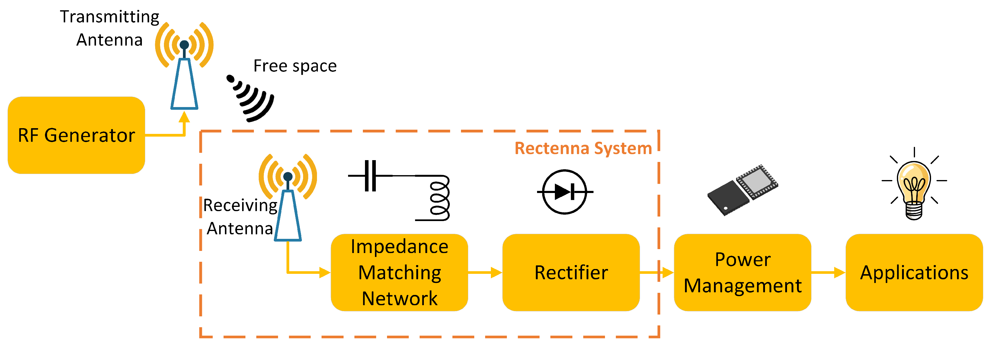
2. Microwave Rectifiers for Ultrawide Power Range Operation

Figure 2 shows a schematic diagram of the proposed dual-module, high-power RF rectifier with an ultrawide dynamic range of input power. The system primarily constitutes the following three key components: a three-port circulator, a Schottky diode-based low-power rectifier (highlighted in green), and an HEMT-based high-power rectifier (highlighted in yellow). The incoming RF power is directed into the three-port circulator (labelled as P1). The diode-based low-power rectifier is connected to the second port of the circulator (P2), while the HEMT-based high-power rectifier is connected to the last port (P3).
An ideal circulator is lossless, with all ports matched but non-reciprocal. In the ideal scenario, the signal enters from one port of the circulator and is completely transmitted to the next port indicated by the arrow (Figure 2). Incident power at any port can be delivered to the adjacent one in rotation without loss, assuming all ports are matched. The signal can only be transmitted in the direction of P1→P2→P3. The following scattering matrix characterizes an ideal three-port circulator:
S = S 21 S 22 S 23 S 31 S 32 S 33 S 11 S 12 S 13 = 1 0 0 0 1 0 0 0 1
Therefore, the incident RF signal can be transferred from P1 to P2 to the diode-based rectifier so that S21 is 1 and all other S-parameter values are 0, which means they are fully isolated. The diode-based rectifier sustains its function of DC generation at a low input power level. When deliberately exposed to excess power, the circulator redirects the reflected power to another appropriately matched high-power HEMT-based rectifier, where S32 is 1. Therefore, high efficiency can be achieved at different input power levels for WPT applications.

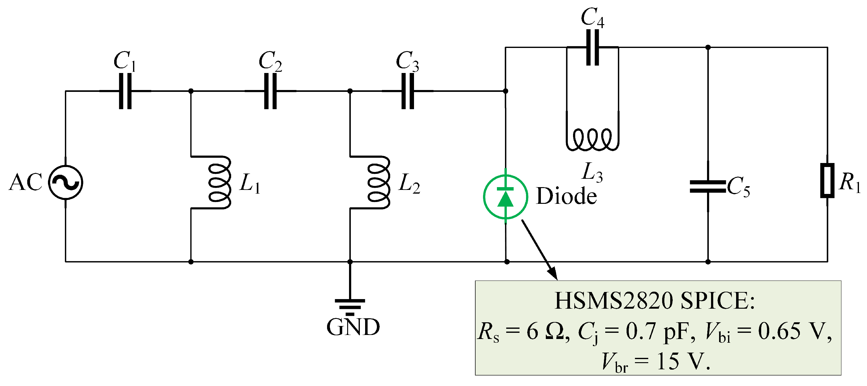
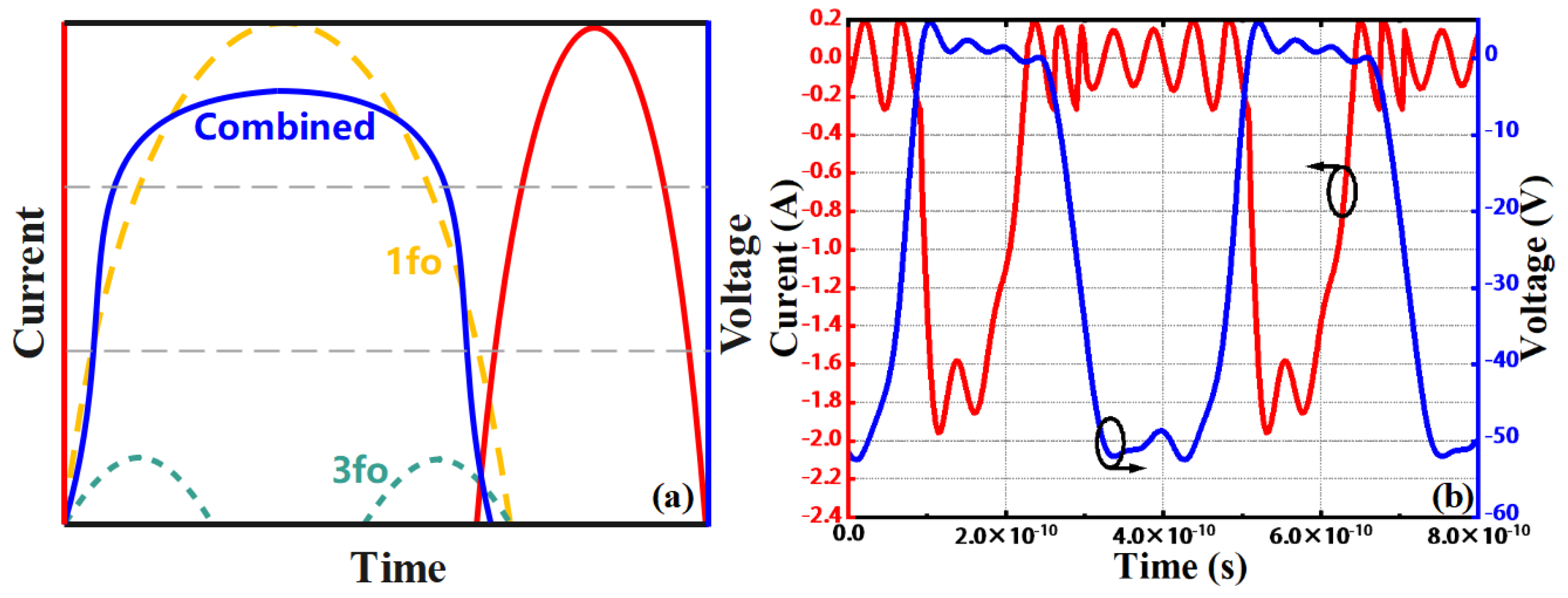
2.1. Low-Power, Diode-Based Rectifier Design

To facilitate the integration of dedicated microwave power transfer in the proposed dual-module rectifier, two aspects of the impedance matching of the low-power diode-based rectifier (Figure 2 green box) should be taken into consideration. Optimizing the RF-to-DC PCE is the primary objective, followed by the secondary goal of maximizing the impedance mismatch for dedicated high-power incidence reflection. The power rectification efficiency at low input power and high-power handling capability of a diode can be improved through crucial considerations, including low built-involtage ( V b i ) and high breakdown voltage ( V b r ) [20,21]. Typically, there exists a contradiction between V b i and V b r due to a primary theoretical challenge, namely that a lower V b i implies a low Schottky barrier height, which leads to a declined V b r . Compared with other commercial diodes, an Avago HSMS2820 Schottky diode with a V b i of less than 0.65 V and a relatively high 15 V breakdown voltage is preferable.
Figure 3 depicts the circuit diagram of a shunt Schottky diode-based rectifier using the SPICE parameters of the diode. C 1 only allows AC power to pass through, whereas DC power will be isolated. L 1 , L 2 , C 2 , and C 3 perform as the impedance-matching network to enhance PCE, while L 3 , C 4 , C 5 , and R 1 function as a low-pass filter to flatten the DC output voltage. The circuit component values are listed in Table 1.
The simulation involves the assessment of the large-signal S parameter to evaluate the impedance-matching characteristics. Optimization with the aim of an S11 value better than −20 dB when the input power is 25 dBm is performed in the Keysight Advanced Design System (ADS). An RF-to-DC PCE exceeding 55% is achieved consistently across an input power range spanning from 12.5 to 29 dBm, as shown in Figure 4. A peak efficiency of 75.9% is attained at a 25.5 dBm RF input level. The PCE starts to decline when the input power increases further. The voltage of the signal exceeds the breakdown voltage of the diode, and consequently, impedance mismatch arises due to the nonlinear diode junction resistance becoming a substantially lower value. Particularly, when the input power is greater than 30 dBm, the PCE falls severely due to the gross mismatch and a huge portion of reflected input power (Figure 5). The reflection can then be recovered by the HEMT-based rectifier, as described in Figure 2, aligning with the high-power optimal-efficiency operating range.

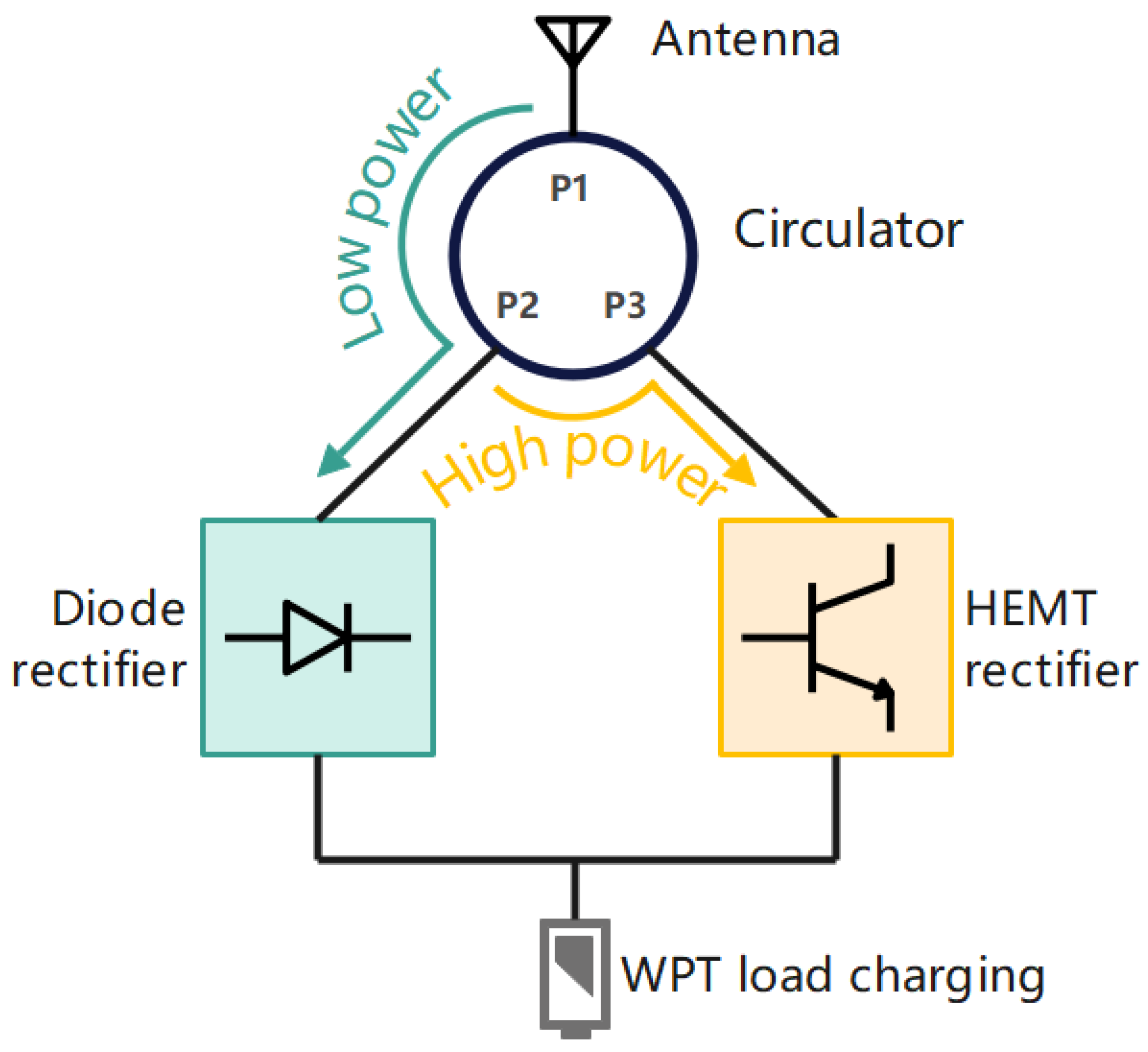
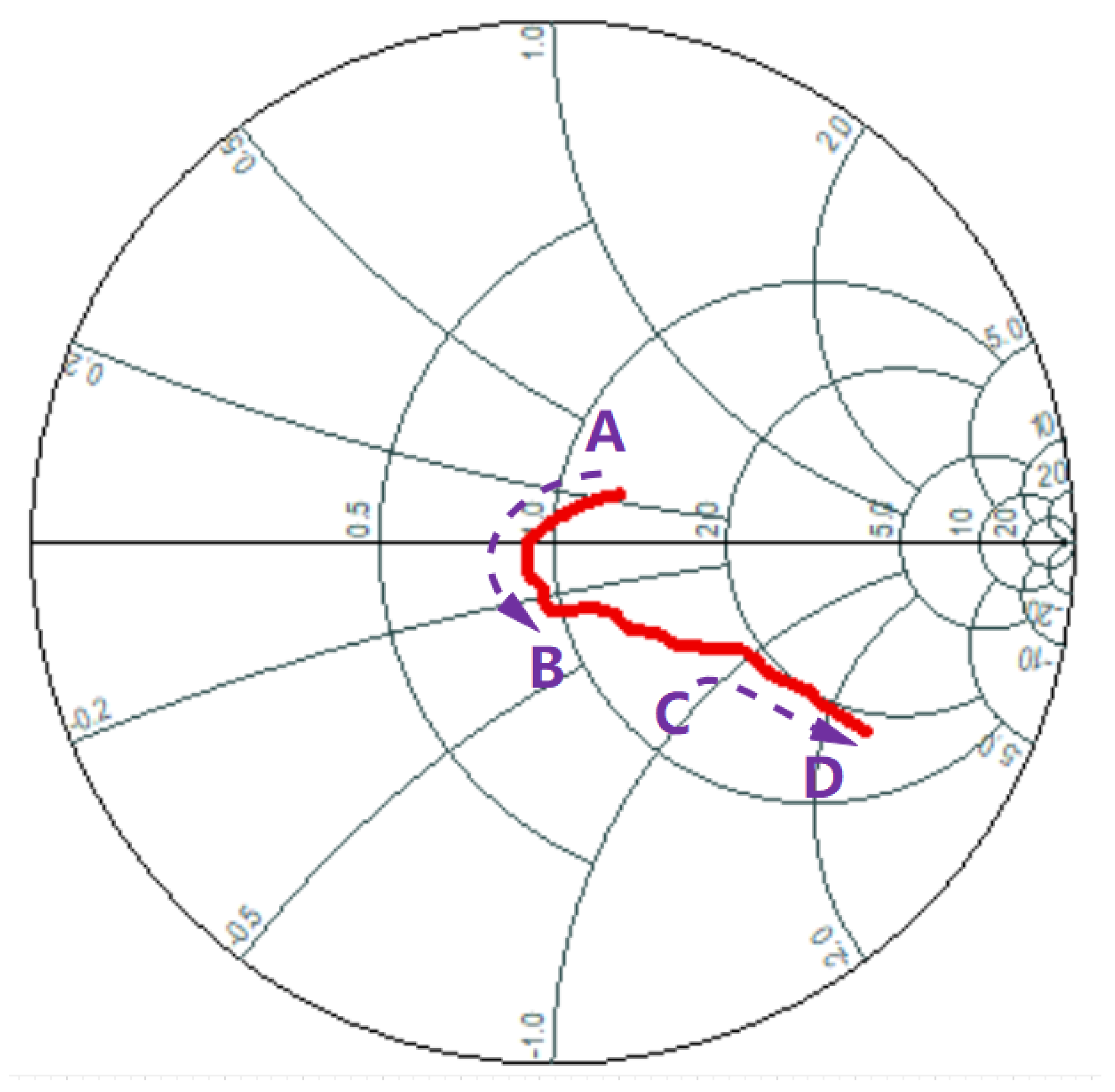
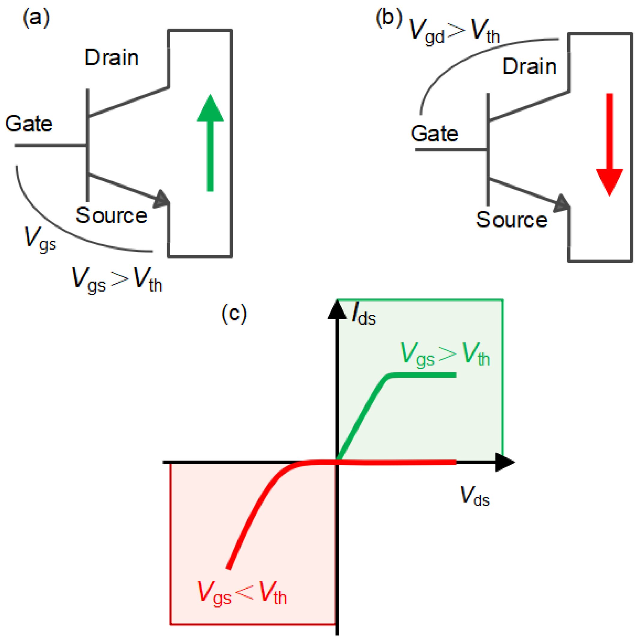
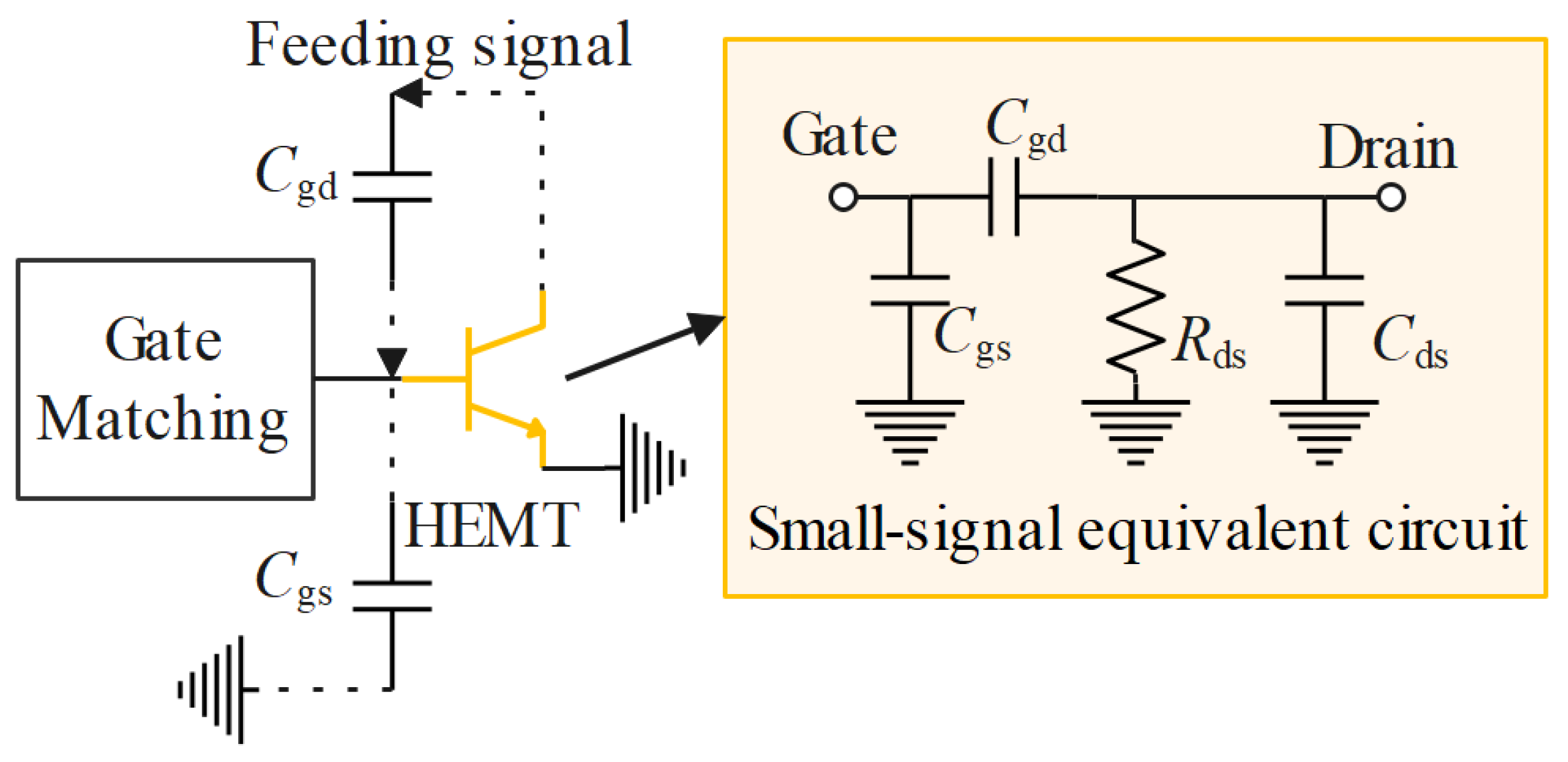
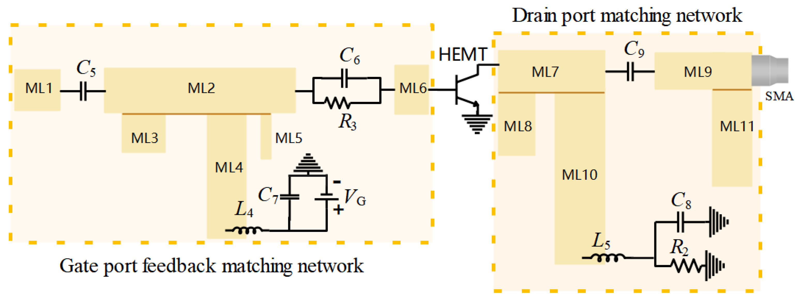
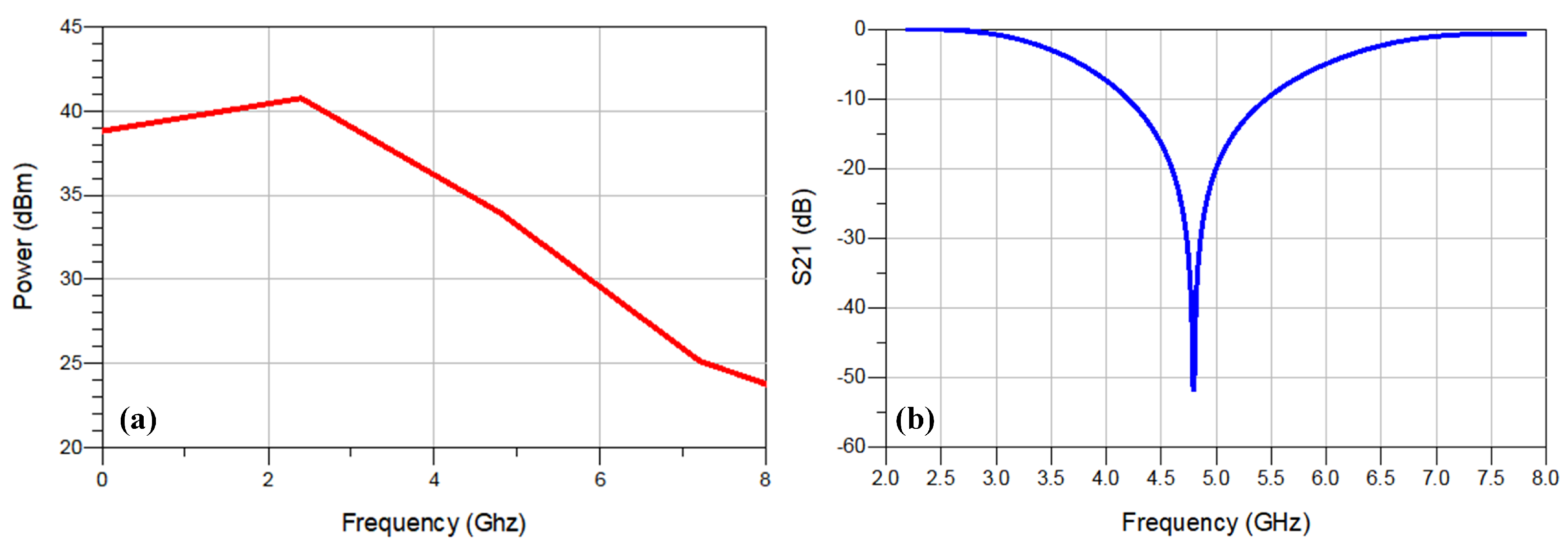
2.2. High-Power Class-F HEMT-Based Rectifier Design

A transistor can be transformed into a rectifier by utilizing its third-quadrant switching characteristic. As depicted in Figure 6a, the criterion for activating the channel in forward conduction (from drain to source, operating in the first quadrant) is that the gate-to-source voltage ( V g s ) must surpass the threshold voltage ( V t h ). When V g s falls below V t h , current cannot conduct in the first quadrant (the power amplifier operation region). The drain and source can be considered interchangeable when the current conducts in the inverted direction. The condition required to open reverse conduction is the gate-to-drain voltage ( V g d ) exceeding V t h (Figure 6b). The transistor operates based on the characteristics exhibited in the third quadrant, as illustrated in Figure 6c and represented by the red curve.
A gate-drive signal is necessary for the self-synchronization of the transistor to achieve autonomous operation as a rectifier without external control and power supply. In previous works, a commonly employed method involved incorporating a sampler with a phase-shifting circuit to generate the required gate signal for the rectifier [22]. However, this approach introduces high complexity in circuit design and increases the overall circuit size. Another method relies on the drain-gate feedback capacitance ( C g d ) inherent in the HEMT, allowing for direct feeding of the RF signal into the gate [23]. This innovative design enables the rectifier to achieve self-synchronization without the need for an external feedback loop. The operating principle of an HEMT-based rectifier is described in Figure 7. When the transistor is considered a switch and RF input power is applied to the drain node, a gate-switching signal is generated through C g d . Consequently, the RF input undergoes rectification by the gate-switching signal.
For high-power operation, a GaN HEMT CGH40010 with high electron mobility and high power is chosen as the rectifying circuit (Figure 2, yellow box). The HEMT-based rectifier design includes a gate feedback-matching network and a drain-matching network. A schematic diagram of the high-power HEMT-based rectifier using a harmonically tuned class-F matching network is shown in Figure 8. Dimensions of the microstrip transmissions, including line widths and lengths, are provided in Table 2. The gate feedback-matching network uses an impedance transformer to maximize power transfer, while the drain-matching network has two stubs (ML8 and ML10) to control the impedance at 2 f o and 3 f o . Harmonic termination networks, particularly the third-harmonic components, are widely used in class-F power amplifier designs to enhance efficiency. The high-efficiency class-F rectifier uses the same principle as the class-F power amplifier, where the RF-to-DC PCE of the rectifier can also be boosted by managing the harmonic components across the HEMT. Figure 9a exhibits that the voltage approximates a square wave, while the current closely resembles a half-rectified sine. The drain network voltage and current waveforms present minimal overlap to minimise power dissipation [24]. The following are the essential requirements for the input impedance at the drain:
Z drain = R optimal fundamental   frequency 0 even   harmonics odd   harmonics
The simulated time-domain current and voltage waveforms at the drain port of the rectifier are represented in Figure 9b, with the RF input power at 41 dBm. This specific value is selected in consideration of the fact that the HEMT in power amplifier operation yields an output power of up to 41 dBm (Figure 10). The presence of C g d enables the rectifier to function in a self-synchronous mode, eliminating the requirement for an extra control signal. Gate feedback matching is terminated with a pure reactance ( X g ) [25] and is designed to optimize the conversion efficiency. The relationship between V g s and V d s can be described as follows:
V g s = 1 C g s C g d 1 X g C g d ω + 1 V d s
The design process employs the ADS harmonic balance circuit simulator, utilizing the non-linear model of the GaN HEMT in the harmonic-balanced circuit analysis. Evaluation metrics include RF-to-DC PCE, output DC power, and large- and small-signal S parameters. The DC load resistance is systematically varied to identify the optimum operational conditions.
The simulation results depicting rectification efficiency and output power are illustrated in Figure 11. The analysis is conducted at an input power ranging from 25 to 41 dBm with a 50 Ω load ( R 2 ). V G is set to −3.8 V, placing the HEMT in the third-quadrant operation region. C 5 (1 pF) and C 9 (4 pF) serve as the matching capacitors, L 4 and L 5 function as choke inductors to prevent shorting of the RF power to the DC, C 7 acts as the DC filter capacitor, and R 3 (3.9 Ω) and C 6 (5 pF) are utilised to improve device stability. In this 2.4 GHz HMET-based rectifier, the matching network is designed based on the large-signal operation conditions. The maximum PCE reaches 77.3% at an RF input power of 36.5 dBm. while a PCE value exceeding 55% is accomplished from 27.5 to 41 dBm (0.56 W to 12.6 W).

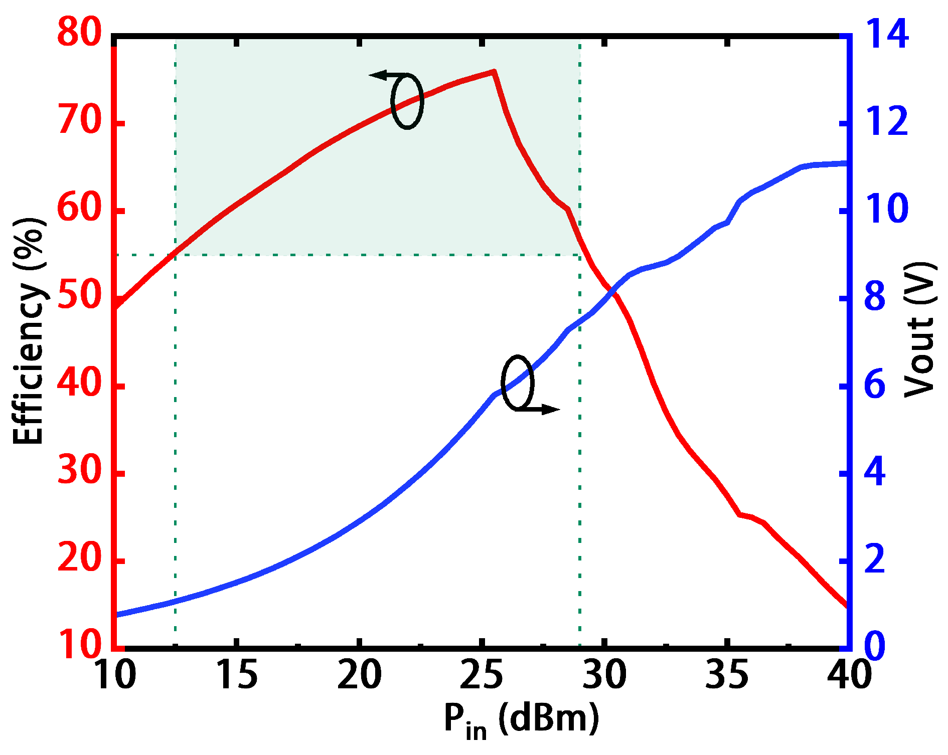
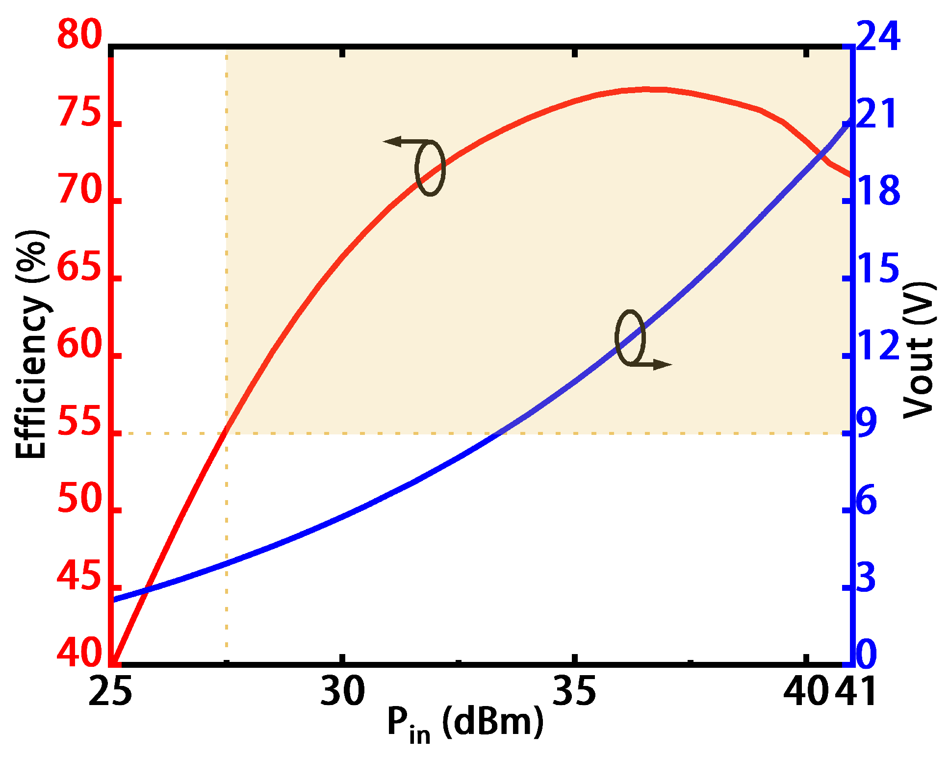
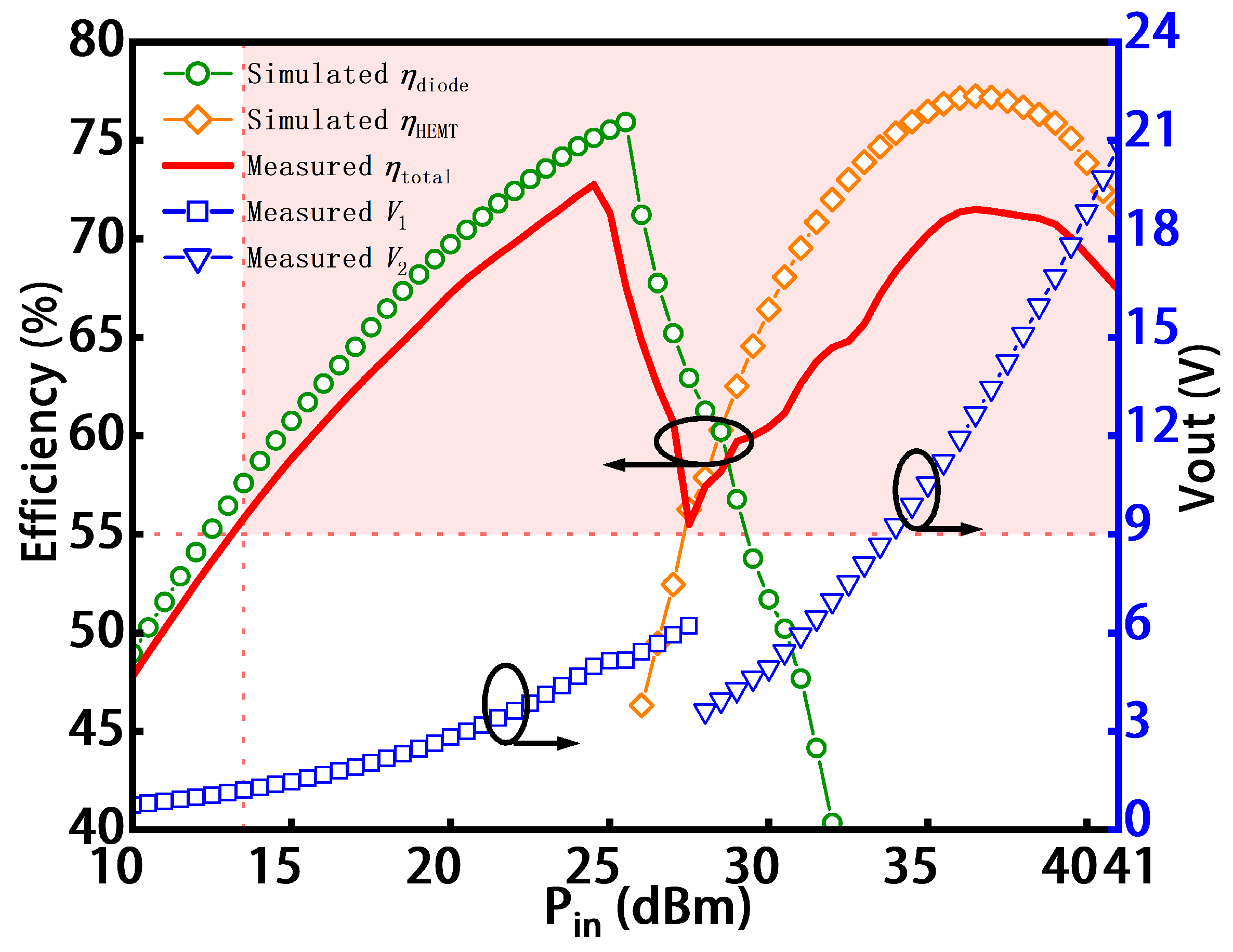
3. Experimental Validation

The rectifier is fabricated as demonstrated in Figure 12. The dual-module rectifier circuit is implemented using microstrip lines on PCBs. To maintain a balance between cost-effectiveness, ease of manufacturing, and the ability to withstand power levels, a 1.6 mm thick FR4 ( ε r = 4.4, tan ( δ ) = 0.03) is selected for the low-power diode-based rectifier, and a 1.52 mm thick Rogers 4350B ( ε r = 3.66, tan ( δ ) = 0.0031) is chosen for the high-power HEMT-based rectifier. The components shown in Figure 3 and Figure 8 are provided by Murata Company, and the microstrip line dimensions presented in Table 2 are slightly adjusted to achieve a compact size. The circulator in shown Figure 12 is provided by UIY company, and the insertion loss and isolation are 0.3 dB and 23 dBm respectively [26].
The measurement setup is shown in Figure 13. The 2.4 GHz RF input power is generated by a Rohde & Schwarz SMB100A. Due to the limited power of the signal output from the generator, the signal is amplified through a driver, then fed into the device under test (DUT). A Keithley 2220G-30-1 supplies the V G to enable HEMT-based rectifier operation. The resulting DC output voltages across two load resistances, namely R 1 and R 2 , are measured using an Agilent Keysight 34411A digital multimeter. The efficiency of the RF-to-DC conversion is determined by the following expression:
η = V 1 2 / R 1 + V 2 2 / R 2 P i n
where V 1 and V 2 are the output DC voltages along R 1 and R 2 , respectively, and P i n is the input power.
The measured rectification efficiency and output DC voltage versus input power are shown in Figure 14. When the input power is 41 dBm (12.6 W) and the gate DC bias is −3.8 V, the measured output DC voltage is 20.87 V, and the rectification efficiency is 68%. The maximum efficiency of 72.8% (diode-based) is recorded for a 24.5 dBm (0.28 W) power input, with an efficiency of 71.5% (HEMT-based) for a 36.5 dBm (4.46 W) power input. Consequently, the rectifier’s operating mode is determined by the input power level, enabling a 27.5 dB (from 13.5 to 41 dBm) ultrawide dynamic range with over 55% conversion efficiency.
In comparison to other state-of-the-art microwave WPT rectifiers, the proposed design demonstrates superior performance, as outlined in Table 3. Notably, the design proposed in [27,28] excels in terms of high input power but exhibits relatively narrow dynamic ranges. On the other hand, the designs proposed in [29,30,31,32] achieve wider dynamic ranges; however, they are solely based on Schottky diode designs and are limited to relatively low power levels for rectification. In contrast, the proposed topology attains high efficiency across a broad input power range, as well as high power-handling capacity, showcasing its usefulness and superior performance.

4. Conclusions

A high-power, high-efficiency RF rectifier suitable for microwave WPT systems is introduced in this paper. A low-loss circulator is used to convey radio frequency energy depending on the input power level. The proposed dual automatic-switching rectifier topology demonstrates superior performance across an ultrawide input power range. Achieving an RF-to-DC power conversion efficiency over 55% within the input power range of 13.5 to 41 dBm (22 mW to 12.6 W), this rectification system holds significant promise in advancing the development of WPT applications.

Author Contributions

Conceptualization, X.Y. (Xiaochen Yu); Methodology, J.Z. (Jinyao Zhang); Software, X.Y. (Xiaochen Yu); Validation, X.Y. (Xiaochen Yu); Formal analysis, J.Z. (Jinyao Zhang); Resources, X.Y. (Xiantao Yang); Writing—original draft, X.Y. (Xiaochen Yu); Writing—review & editing, M.L. and J.Z. (Jiafeng Zhou); Supervision, T.-J.Y. and J.Z. (Jiafeng Zhou); Project administration, Y.H. and J.Z. (Jiafeng Zhou). All authors have read and agreed to the published version of the manuscript.

Funding

This project is funded by National Tsing Hua University and the University of Liverpool Dual PhD programme and EPSRC IAA (Ref: EP/X525741/1).

Data Availability Statement

The original contributions presented in the study are included in the article, further inquiries can be directed to the corresponding author.

Conflicts of Interest

The authors declare no conflicts of interest.

References

  1. Mohamed, A.A.S.; Lashway, C.R.; Mohammed, O. Modeling and Feasibility Analysis of Quasi-Dynamic WPT System for EV Applications. IEEE Trans. Transp. Electrif. 2017, 3, 343–353. [Google Scholar] [CrossRef]
  2. Chen, H.; Qian, Z.; Zhang, R.; Zhang, Z.; Wu, J.; Ma, H.; He, X. Modular Four-Channel 50 kW WPT System with Decoupled Coil Design for Fast EV Charging. IEEE Access 2021, 9, 136083–136093. [Google Scholar] [CrossRef]
  3. Jiang, Y.; Wang, L.; Wang, Y.; Liu, J.; Wu, M.; Ning, G. Analysis, Design, and Implementation of WPT System for EV’s Battery Charging Based on Optimal Operation Frequency Range. IEEE Trans. Power Electron. 2019, 34, 6890–6905. [Google Scholar] [CrossRef]
  4. Zeng, Y.; Qiu, D.; Meng, X.; Zhang, B.; Tang, S.C. Optimized Design of Coils for Wireless Power Transfer in Implanted Medical Devices. IEEE J. Electromagn. Microw. Med. Biol. 2018, 2, 277–285. [Google Scholar] [CrossRef]
  5. Yang, X.T.; Wong, H.; Xiang, J. Polarization Reconfigurable Planar Inverted-F Antenna for Implantable Telemetry Applications. IEEE Access 2019, 7, 141900–141909. [Google Scholar] [CrossRef]
  6. Pahlavan, S.; Shooshtari, M.; Jafarabadi Ashtiani, S. Star-Shaped Coils in the Transmitter Array for Receiver Rotation Tolerance in Free-Moving Wireless Power Transfer Applications. Energies 2022, 15, 8643. [Google Scholar] [CrossRef]
  7. Pahlavan, S.; Jafarabadi-Ashtiani, S.; Mirbozorgi, S.A. Maze-Based Scalable Wireless Power Transmission Experimental Arena for Freely Moving Small Animals Applications. IEEE Trans. Biomed. Circuits Syst. 2024, 1–10. [Google Scholar] [CrossRef] [PubMed]
  8. Wang, X.; Li, L.; Cui, T.J.; Lu, M. On Differentiation Among Pilot Signals of Multiple Mobile Targets in Retro-Reflective Beamforming for Wireless Power Transmission. Engineering 2023, 30, 55–62. [Google Scholar] [CrossRef]
  9. Li, X.; Duan, B.; Zhang, Y.; Guo, Y. Optimal Design of Aperture Illuminations for Microwave Power Transmission with Annular Collection Areas. Engineering 2023, 30, 63–74. [Google Scholar] [CrossRef]
  10. Liu, Z.; Hu, H.; Su, Y.G.; Sun, Y.; Chen, F.; Deng, P. A Double-Receiver Compact SCC-WPT System with CV/CC Output for Mobile Devices Charging/Supply. IEEE Trans. Power Electron. 2023, 38, 9230–9245. [Google Scholar] [CrossRef]
  11. Peng, C.; Ye, Z.; Wu, J.; Chen, C.; Wang, Z. Design of a Wide-Dynamic RF-DC Rectifier Circuit Based on an Unequal Wilkinson Power Divider. Electronics 2021, 10, 2815. [Google Scholar] [CrossRef]
  12. Gao, S.P.; Ou, J.H.; Zhang, X.; Guo, Y. Scavenging Microwave Wireless Power: A Unified Model, Rectenna Design Automation, and Cutting-Edge Techniques. Engineering 2023, 30, 32–48. [Google Scholar] [CrossRef]
  13. Takabayashi, N.; Kawai, K.; Mase, M.; Shinohara, N.; Mitani, T. Large-Scale Sequentially-Fed Array Antenna Radiating Flat-Top Beam for Microwave Power Transmission to Drones. IEEE J. Microw. 2022, 2, 297–306. [Google Scholar] [CrossRef]
  14. Barnett, R.E.; Liu, J.; Lazar, S. A RF to DC Voltage Conversion Model for Multi-Stage Rectifiers in UHF RFID Transponders. IEEE J. Solid-State Circuits 2009, 44, 354–370. [Google Scholar] [CrossRef]
  15. Hamill, D. Time reversal duality and the synthesis of a double class E DC-DC converter. In Proceedings of the 21st Annual IEEE Conference on Power Electronics Specialists, San Antonio, TX, USA, 11–14 June 1990; pp. 512–521. [Google Scholar] [CrossRef]
  16. Abbasian, S.; Johnson, T. Power-Efficiency Characteristics of Class-F and Inverse Class-F Synchronous Rectifiers. IEEE Trans. Microw. Theory Tech. 2016, 64, 4740–4751. [Google Scholar] [CrossRef]
  17. You, F.; Dong, S.; Wang, Y.; Yu, X.; Li, C. Design Method of Self-Driving RF-DC Rectifier Based on Waveform-Guided Solutions to Passive Matching Network. IEEE Trans. Power Electron. 2019, 34, 6498–6509. [Google Scholar] [CrossRef]
  18. Abbasian, S.; Johnson, T. High efficiency and high power GaN HEMT inverse class-F synchronous rectifier for wireless power applications. In Proceedings of the 2015 European Microwave Conference (EuMC), Paris, France, 7–10 September 2015; pp. 299–302. [Google Scholar] [CrossRef]
  19. Roberg, M.; Reveyrand, T.; Ramos, I.; Falkenstein, E.A.; Popovic, Z. High-Efficiency Harmonically Terminated Diode and Transistor Rectifiers. IEEE Trans. Microw. Theory Tech. 2012, 60, 4043–4052. [Google Scholar] [CrossRef]
  20. Liu, K.; Wang, C.; Zheng, X.; Ma, X.; He, Y.; Li, A.; Zhao, Y.; Mao, W.; Hao, Y. Effect of post anode annealing on W/Au and Ni/Au multi-channel AlGaN/GaN Schottky diode. Superlattices Microstruct. 2021, 160, 107089. [Google Scholar] [CrossRef]
  21. Takahashi, K.; Ao, J.P.; Ikawa, Y.; Hu, C.Y.; Kawai, H.; Shinohara, N.; Niwa, N.; Ohno, Y. GaN Schottky Diodes for Microwave Power Rectification. Jpn. J. Appl. Phys. 2009, 48, 04C095. [Google Scholar] [CrossRef]
  22. Zhang, Z.; Cheng, Z.; Fusco, V.; Buchanan, N.; Gu, C. Dual-Band GaN Transistor-Based RF-DC Rectifier. In Proceedings of the 2021 Cross Strait Radio Science and Wireless Technology Conference (CSRSWTC), Shenzhen, China, 11–13 October 2021; pp. 202–204. [Google Scholar] [CrossRef]
  23. Zhang, J.; Huang, Y.; Zhou, J. A Wide Dynamic Range Rectifier Based on HEMT With a Variable Self-Bias Voltage. IEEE Trans. Circuits Syst. II Express Briefs 2024, 71, 547–551. [Google Scholar] [CrossRef]
  24. Raab, F. Maximum efficiency and output of class-F power amplifiers. IEEE Trans. Microw. Theory Tech. 2001, 49, 1162–1166. [Google Scholar] [CrossRef]
  25. Yamazaki, J.; Ishikawa, R.; Honjo, K. Input-Power-Synchronous Adaptively Biased Wide-Dynamic-Range High-Efficiency Rectifier with Zero-Threshold GaAs HEMTs. In Proceedings of the 2020 50th European Microwave Conference (EuMC), Utrecht, The Netherlands, 12–14 January 2021; pp. 436–439. [Google Scholar] [CrossRef]
  26. UIY. 700 to 5000 MHz—Coaxial Circulator. Available online: https://www.uiy.com/Datasheet/UIYCC2528A.pdf (accessed on 29 May 2024).
  27. Zhang, Z.; Gu, C.; Cheng, Z.; Xuan, X. Design a GaN HEMT-Based Broadband High-Efficiency Rectifier Using a Wideband Phase Shift Structure. IEEE Microw. Wirel. Technol. Lett. 2023, 33, 751–754. [Google Scholar] [CrossRef]
  28. Zhang, Z.; Fusco, V.; Cheng, Z.; Buchanan, N.; Gu, C. A Transistor-Based Dual-Band High-Efficiency Rectifier with Dual-Polarity Modes. IEEE Microw. Wirel. Compon. Lett. 2022, 32, 169–172. [Google Scholar] [CrossRef]
  29. Xiao, Y.Y.; Du, Z.X.; Zhang, X.Y. High-Efficiency Rectifier With Wide Input Power Range Based on Power Recycling. IEEE Trans. Circuits Syst. II Express Briefs 2018, 65, 744–748. [Google Scholar] [CrossRef]
  30. Zheng, S.Y.; Wang, S.H.; Leung, K.W.; Chan, W.S.; Xia, M.H. A High-Efficiency Rectifier With Ultra-Wide Input Power Range Based on Cooperative Structure. IEEE Trans. Microw. Theory Tech. 2019, 67, 4524–4533. [Google Scholar] [CrossRef]
  31. Wu, P.; Chen, Y.d.; Zhou, W.; Ren, Z.H.; Huang, S.Y. A Wide Dynamic Range Rectifier Array Based on Automatic Input Power Distribution Technique. IEEE Microw. Wirel. Compon. Lett. 2020, 30, 437–440. [Google Scholar] [CrossRef]
  32. Kim, J.; Oh, J. Compact Rectifier Array with Wide Input Power and Frequency Ranges Based on Adaptive Power Distribution. IEEE Microw. Wirel. Compon. Lett. 2021, 31, 513–516. [Google Scholar] [CrossRef]
Figure 1. Block diagram of an RF WPT system.
Energies 17 02707 g001
Figure 2. Diagram of the proposed dual-module rectifier with an ultrawide dynamic power range.
Energies 17 02707 g002
Figure 3. Diagram of the low-power, diode-based rectifier circuit with SPICE parameters. The SPICE parameters of the diode consist of the series resistance ( R s ), the junction capacitance ( C j ), the built-involtage ( V b i ), and the breakdown voltage ( V b r ).
Energies 17 02707 g003
Figure 4. Simulated RF-to-DC rectification efficiency and DC output voltage along R 1 versus input RF power for the low-power, diode-based rectifier. The region of efficiency over 55% is highlighted in the green box. The signal is transferred from P1 to P2 of the circulator.
Energies 17 02707 g004
Figure 5. Simulated S11 at P1 of the circulator in a Smith chart (The input power at A is 20 dBm, at B is 30 dBm, at C is 35 dBm, and at D is 40 dBm). A 64.5% power reflection occurs at C, corresponding to S11 = −1.9 dB.
Energies 17 02707 g005
Figure 6. Requirements for activation of the channel of an HEMT: (a) forward conduction; (b) reverse conduction; (c) behavior of a transistor in the 1st quadrant (green curve, power amplifier operation model) and the 3rd quadrant (red curve, rectifier operation model).
Energies 17 02707 g006
Figure 7. Principle of HEMT-based rectifier operation with C g d direct feeding of the RF signal from the drain to the gate.
Energies 17 02707 g007
Figure 8. Circuit topology of the realized matching network of the HEMT-based rectifier.
Energies 17 02707 g008
Figure 9. Class-F time-domain current and voltage waveforms: (a) ideal half-rectified sine wave and square voltage waveform obtained by managing the odd harmonic; (b) simulated waveforms at 2.4 GHz (the RF input power at the drain is 41 dBm).
Energies 17 02707 g009
Figure 10. Simulated HEMT power amplifier operation characteristics: (a) output power of 41 dBm at 2.4 GHz; (b) drain output matching network S21 versus frequency.
Energies 17 02707 g010
Figure 11. Simulated output DC power and rectification efficiency versus input RF power for the high-power HEMT-based rectifier, emphasising the efficiency greater than 55% in the yellow box. The signal is transferred from P1 to P3 of the circulator.
Energies 17 02707 g011
Figure 12. Photo of the proposed ultrawide-dynamic-range power rectifier.
Energies 17 02707 g012
Figure 13. Measurement setup of the rectifier. DUT represents the fabricated circuit shown in Figure 12.
Energies 17 02707 g013
Figure 14. Simulated and measured efficiencies and DC output voltages of the proposed rectifier. The PCE region greater than 55% from 13.5 to 41 dBm is highlighted by the red box.
Energies 17 02707 g014
Table 1. Circuit component values of the realized matching network for a diode-based rectifier.
Circuit ComponentValue
C 1 100 pF
C 2 0.7 pF
C 3 0.4 pF
C 4 2.7 pF
C 5 1.0 uF
L 1 3.4 nH
L 2 3.3 nH
L 3 1.4 nH
R 1 200 Ω
Table 2. Microstrip line dimensions for HMET-based rectifier matching networks.
Microstrip LineDimensions: mm × mm
ML13.9 × 3.29
ML214.4 × 3.29
ML33.6 × 3.29
ML414.5 × 3.29
ML55.4 × 1.00
ML62.0 × 3.29
ML710.3 × 4.50
ML86.6 × 3.29
ML910.5 × 3.29
ML1017.6 × 4.90
ML119.6 × 3.29
Table 3. Comparison with the previous RF rectifiers.
Reference/Year Frequency
(GHz)
DeviceTopology Peak Pin
(W)
 Peak PCE
(%)
Pin Range (dB)
for Efficiency
over 55%
[27]/20232.6GaN HEMTClass- F 1
phase shift
108617
[28]/20221.9/2.4GaN HEMTClass-F
phase shift
1075/7615/13
[29]/20182.453 Schottky DiodesBranch-line
coupler
16224
(PCE > 50%)
[30]/20192.42 Schottky DiodesCooperative
structure
0.3572.823
[31]/20202.42 Schottky DiodesDoherty
concept
181.222.5
[32]/20212.454 Schottky DiodesDoherty
concept
1.267.520.3
This work2.41 HEMT &
1 Diode
Dual-model
cooperation
12.672.727.5
Disclaimer/Publisher’s Note: The statements, opinions and data contained in all publications are solely those of the individual author(s) and contributor(s) and not of MDPI and/or the editor(s). MDPI and/or the editor(s) disclaim responsibility for any injury to people or property resulting from any ideas, methods, instructions or products referred to in the content.

