Article

Multiphase LLC DC-Link Converter with Current Equalization Based on CM Voltage-Controlled Capacitor

1
Delta Electronics Inc., No. 186, Ruiguang Rd., Neihu Dist., Taipei City 114501, Taiwan
2
Department of Electrical Engineering, National Taipei University of Technology, No. 1, Sec. 3, Zhongxiao E. Rd., Taipei 10608, Taiwan
*
Author to whom correspondence should be addressed.
Energies 2024, 17(11), 2793; https://doi.org/10.3390/en17112793
Submission received: 3 May 2024 / Revised: 26 May 2024 / Accepted: 3 June 2024 / Published: 6 June 2024
(This article belongs to the Special Issue Energy, Electrical and Power Engineering 2024)

Abstract

:
In this study, a current-equalization technology utilizing a variable-capacitance technique for a multiphase inductor–inductor–capacitor (LLC) converter is studied. Accordingly, the proposed method involves adjusting the resonant capacitance of the LLC resonant converter to balance the currents between phases. This is achieved primarily by biasing ferroelectric multilayer ceramic capacitors (MLCCs) through a step-down circuit and a common-mode bias structure. These ferroelectric MLCCs serve as the resonant elements, allowing for variable capacitance by leveraging capacitance sensitivity to their trans voltages. This approach provides additional control flexibility to the resonant circuit. Furthermore, since each phase operates independently, the circuit can be scaled to accommodate any number of phases. Moreover, all switches in the circuit have zero-voltage switching (ZVS) turn-on, minimizing switching losses. This study initially analyzes and evaluates the proposed common-mode bias variable capacitance technique and the corresponding operational principles. Subsequently, a two-phase LLC experimental circuit based on a field-programmable gate array (FPGA) digital controller is utilized to assess current equalization and efficiency. That is to say, this experimentation aims to validate the effectiveness of the current-equalization variable-capacitance technique in an LLC resonant converter.

1. Introduction

With the increase in energy awareness and the requirements of related regulations, high-efficiency energy processing has become an important issue nowadays. In particular, since electricity is the most commonly used energy source in daily life due to its ease of transmission and use, its energy efficiency is particularly important. In order to improve the efficiency of home electricity and reduce energy consumption, appliances such as air conditioners, refrigerators, DC fans, etc., can adjust their power consumption according to the load conditions. In addition, the popularity of solid-state lighting systems has led to the adoption of DC constant-current power supplies for light source drivers. All of these applications require the rectification of utility power to DC power and further DC conversion through power electronics. With the popularity of power electronics in the home, the cost and power loss of bridge rectifiers have increased, and the harmonic pollution of AC power supplies has become a major concern.
If the power can be supplied by 100 V~240 V DC voltage, the above problem can be improved without changing the existing residential power wiring. In this paper, a multiphase DC-link voltage converter based on variable-capacitor active current equalization is implemented to reduce the medium-voltage DC power output from the front-end PFC circuit to a DC power source that can be applied to an indoor power distribution line, as shown in Figure 1.
An isolated fixed ratio DC-link voltage converter is a type of an isolated converter with voltage gain close to some constant value, and this type is usually combined with a pre- or post-stage voltage regulator. This voltage regulator can be found in data centers, telecommunication base stations, battery storage systems, DC microgrids, etc., where it serves as a DC step-up or step-down converter. Since this converter is a component of a multi-stage system, it requires a high-efficiency conversion; therefore, a resonant power converter is used to realize soft switching to improve efficiency.
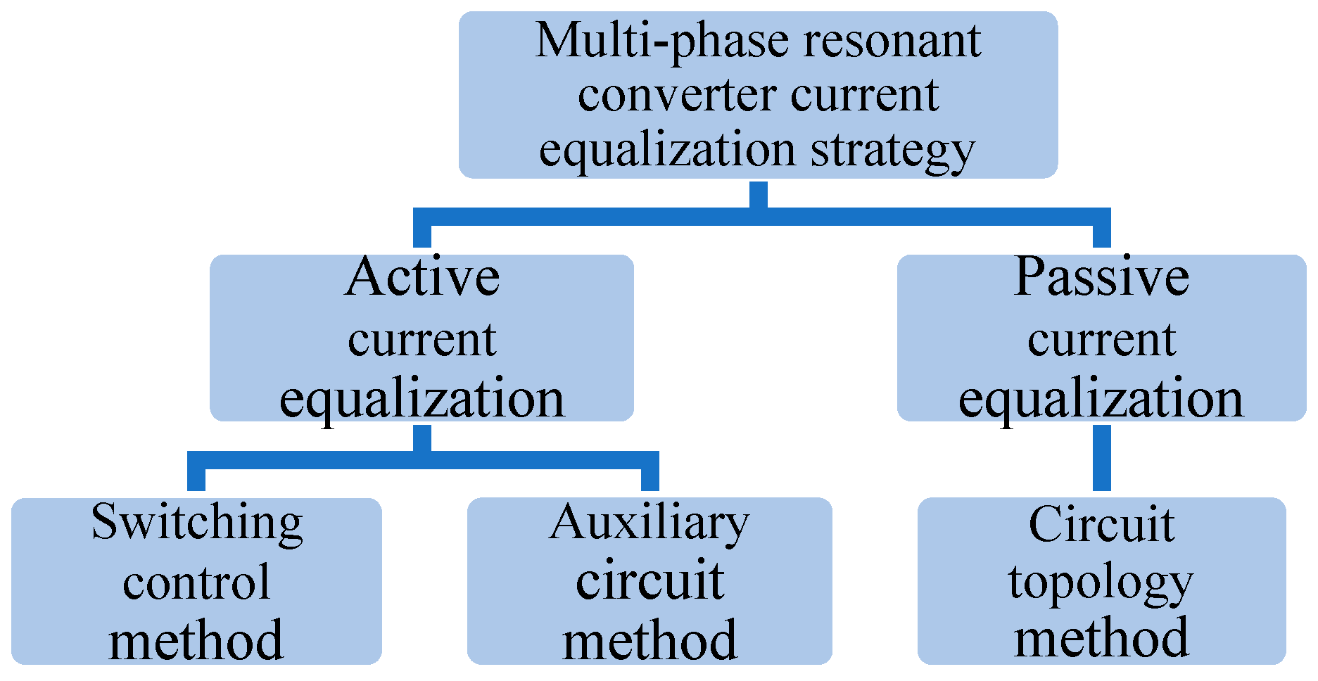
On the other hand, the low-amplitude, high-frequency nature of the output current ripple of a typical multiphase power converter allows the use of smaller filter elements in high-power applications [1]. However, the tolerance of the components will cause the impedance of the resonant tanks of the multiphase resonant power converter to differ from one phase to another, and this deviation will result in a phase current imbalance. Overloading of local circuits may cause problems such as saturation of magnetic components, overheating of semiconductor components, or degradation of conversion efficiency. Therefore, the issue of current equalization should be considered in practical applications, and many corresponding strategies have been presented as shown in Figure 2.
Currently, the current-equalization strategies shown in Figure 2 for multiphase resonant power converters can be classified into three main categories based on their technologies, which are circuit topology, switching regulation, and auxiliary circuits. Among them, the circuit topology method achieves the purpose of current equalization based on the resonant circuit topology, and most of these techniques do not introduce additional control degrees of freedom; thus, they are classified as passive current-equalization strategies. One study in the literature [2] proposes a current-equalization strategy for connecting resonant capacitor nodes, whereas another study [3] proposes a current-equalization strategy for connecting resonant inductor nodes. The literature [4,5,6] suggests a transformer coupling or staggered connection of windings to achieve current equalization. In addition, current equalization can be achieved by applying an external capacitor to obtain ampere-second balance [7]. All of the above techniques achieve phase current balancing through the circuit topology method, thereby eliminating the need for additional control of the main switches. However, the output ripple of the multiphase circuit is still comparable to that of a single-phase circuit due to the need for additional circuit connections or the existence of flux coupling, and this makes it necessary to synchronize the switching of each phase; therefore, an output filter-based current-equalization method is proposed in [8]. In [9,10], a common-mode choke is used to equalize the current in a three-phase converter. The literature [2,3,4,5,6,7,8,9,10] reports the use of additional components or circuits to achieve phase current equalization.
Compared to the above topologies, the switching control method [11,12,13,14] and the auxiliary circuit method [15,16,17,18,19] are classified as active current-equalization strategies, where the switching frequency or duty cycle of the switch is varied as an additional control degree of freedom. In particular, the technique of equalizing the current flow by regulating the switch has the advantage of a relatively low cost because it does not require the use of additional auxiliary circuits. In this method, the switching frequency [11] and the voltage phase difference [12,13,14] are used as the control degrees of active equalization. However, the method of balancing the output current by the switching frequency of each phase does not allow the switching phase angle to be constant and thus has relatively large output voltage ripple; regardless, this method is based on typical frequency modulation and is relatively easy to implement [11]. The current-equalization method using the phase difference between the input voltages of the resonant tanks requires the synchronization of the resonant current phases in order to avoid loss of zero-voltage switching (ZVS) turn-on of the switch, and this leads to an increase in switching loss. However, since this method requires the same switching frequency in each phase, it has relatively low output voltage ripple [12,13,14].
In contrast to the switching control method, the auxiliary circuit method utilizes an additional circuit for phase current balancing. This additional circuit can be a pre- or post-converter [15], a low-power circuit designed for partial power handling [16,17], or a resonant tank regulation circuit [18,19]. Since the phase current balancing is achieved by the auxiliary circuit, the current-equalization controller and the main-loop controller can usually be operated independently, which is a less complex control method than the switching control method. However, the additional cost and losses of the auxiliary circuits must be considered in practical applications. The variable-capacitor current-equalization technique proposed in this paper is a branch of this technique because the auxiliary circuit is used to build up the capacitor bias. However, the bias circuit is quite low in power, and all the switches are capable of ZVS turn-on; thus, the conversion efficiency can be maintained at a high level.
On the other hand, in the case of a resonant converter, it can be regarded as a circuit in which the impedance is adjusted by the operating frequency. Since the impedance of the resonant tank is easily affected by the switching frequency, the tolerance of the passive components will cause the resonant frequency to shift, resulting in the actual impedance deviating from the desired value. However, if the parameters of the resonant passive components can be adjusted, it is possible to bring about a controllable impedance feature. Therefore, the idea of applying variable inductor and capacitor technologies to resonant power converters has been investigated.
In the case of variable inductors, the principle is mainly based on controllable magnetoresistance. In this case, the reluctance can be varied by changes in the cross-sectional area of the magnetic circuit, the length of the magnetic circuit, and the magnetic permeability of the material. One report in the literature [20] shows a variable inductor with an adjustable air-gap width, while another study [21] proposes a variable inductor based on ferromagnetic fluid of microelectromechanical systems (MEMS). In addition, the literature [22,23,24,25,26] applies the phenomenon that the relative permeability of ferromagnetic materials decreases with increasing magnetic field strength to realize variable inductors. In this type of device, there exist a set of auxiliary windings and a controlled current source, and the inductance is adjusted by regulating the current of the auxiliary windings to build up the corresponding bias field strength. Since the auxiliary windings are independent of the main winding, the auxiliary circuit operation is not affected by the floating potential of the main winding. However, an additional auxiliary winding will increase the size of the components, and the losses due to the bias current need to be fully considered to minimize the impact on the conversion efficiency. The literature [27] presents current sharing based on detecting thermal runaway and controlling current ramping-down time.
In terms of variable capacitance, it is mainly controlled by adjusting the electrode area, electrode spacing, and material permittivity to change the capacitance value. Among these options, a varactor diode based on the semiconductor process changes the capacitance by adjusting the width of the empty area, and the adjustment of capacitance with the help of microelectromechanical technology can achieve the same purpose through the change of the microstructure [28,29,30,31]. As for the nonlinear dielectric, the capacitance of a liquid crystal as the dielectric is changed by an applied electric field and increases with the increase in the control voltage [32]. However, such a technique is usually applied to the frequency tuning and line impedance matching of the radio frequency (RF) filter; thus, the capacitor used have a lower withstand voltage and lower capacitance, making it difficult to apply to the resonant power converter.
Since the resonant capacitance requirement of a resonant power converter is usually higher than that of an RF circuit, the use of nonlinear ferroelectric ceramics with high permittivity as dielectrics in this application can maintain the advantage of high capacitance density based on the adjustable capacitance. The literature [33] proposes a variable capacitor at the component level, in which the capacitance of the ferroelectric dielectric is varied by controlling the electric field between the electrodes to achieve capacitance tuning. Class II multilayer ceramic capacitors (MLCCs) under the EIA RS-198 specification also commonly use nonlinear ferroelectric material as the dielectric [34], and if the biasing characteristics of this type of capacitor can be utilized, capacitance adjustment can be achieved by conventional MLCCs. This approach offers higher design flexibility than the component-level variable capacitor, and the idea has been validated in wireless power transmission systems [35,36,37]. A typical structure, shown in Figure 3, realizes the variable capacitor by biasing the ferroelectric MLCC, i.e., the DC bias is constructed by an auxiliary current source on the nonlinear capacitors Cr1 and Cr2 to realize the capacitance control, and the equivalent capacitance is equivalent to the capacitance of two capacitors connected in series.
The variable capacitors described above for radio energy transmission are also suitable for use in multiphase resonant power converters, where the variable capacitance technology is used to balance the impedance of the resonant tanks of the various phases in order to achieve equalization of the converter currents. In addition, the high AC voltage swing of the resonant capacitor to ground makes typical biasing structures require the use of high-impedance current sources or isolated control circuits, thereby increasing the difficulty of realizing this technology.
Accordingly, this paper proposes a common-mode bias structure for isolated converters, which can effectively reduce the AC amplitude of the bias node by extracting the common-mode voltage component of the resonant capacitor through a center-tap transformer. As a result, a non-isolated switching power supply structure can be selected for the bias circuit to significantly increase the bias operating range, and the capacitive impedance of the bias node eliminates the need for an additional filter capacitor. In this paper, a synchronous rectifier buck circuit is used to build up the bias node, and the proposed common-mode bias variable capacitance technique is verified by a two-phase inductor–inductor–capacitor (LLC) DC-link voltage converter to be practically applicable to the current equalization of multiphase resonant circuits.

2. Principle of Current Equalization Based on a Variable Capacitor

Resonant converters are mostly operated near the resonant frequency, and the voltage gain is regulated by the fact that the impedance of the resonant tank is sensitive to the frequency of the excitation signal. Since the frequencies of the switching voltage harmonic waveforms are far from the resonant frequency, the fundamental component of this excitation signal will dominate the characteristics of voltage gain and impedance of the converter. The fundamental elements, together with load equivalent resistance, are used to approximate the converter characteristics, and this is called the first harmonic approximation (FHA).
Since the output rectifier exhibits nonlinearity, it is common to extract the load impedance to the front of this rectifier, and this impedance can be expressed in terms of the AC equivalent resistance, Rac, as described below:
R a c = 8 R L n π 2
The FHA model of the LLC resonant converter is shown in Figure 4, where the impedances of the resonant components Cr, Lr, and Lm at the switching frequency fs can be described by (2) to (5), respectively. The voltage gain M can be expressed based on the AC equivalent resistance Rac and the voltage division.
Z C r = 1 j × 2 π f s × C r
Z L r = j × 2 π f s × L r
Z L m = j × 2 π f s × L m
M = R a c × Z L m R a c + Z L m × Z C r + Z L r + R a c × Z L m R a c + Z L m 1
Figure 5a shows the relationship among voltage gain, resonant capacitance, and resonant inductance for a light load of RL = 25 Ω. Figure 5b shows the relationship among the resonant tank voltage gain, resonant capacitance, and resonant inductance for a rated load of RL = 250 Ω. The voltage gain trends of the two loads are similar. The greater the resonant inductance deviation is, the lesser the voltage gain, whereas the greater the resonant capacitance is, the lesser the voltage gain, implying that the lesser the DC bias is, the greater the voltage gain.
The basic reason for phase current imbalance is the difference in the voltage gain of each phase converter, as shown by the dotted lines in Figure 5a,b, where 100% Lr is the nominal resonant inductance. If a combination of resonant parameters can be found so that the voltage gain of each phase circuit is the same, then current equalization can be achieved. From these figures, the greater the resonant inductance is, the lower the voltage gain, and therefore the lesser the resonant capacitance required to increase the voltage gain. The capacitance adjustment range of the proposed technique depends on the characteristics of ferroelectric MLCCs and the bias range. From the above analysis, it can be ascertained that the widest capacitance adjustment range is required when the resonant inductance of each phase resonant inductance locates between 100% Lr and 150% Lr, and therefore, the experimental circuits are designed under this worst-case condition in order to make sure that the proposed circuits can compensate for any resonant inductance deviation within the design range and realize not only voltage gain balance but also current equalization.
To speak more lucidly, Figure 5 shows the effect of resonant parameters on voltage gain when the switching frequency is fixed. From this figure, it can be seen that the deviation of the resonant inductance Lr will cause the voltage gain to be changed, which is the main reason for load current imbalance of a multi-phase converter. The change in voltage gain can be compensated by adjusting the resonant capacitance Cr. This is the reason why the proposed circuit uses variable capacitors to achieve load current equalization.

3. Common-Mode Bias Variable Capacitance Structure

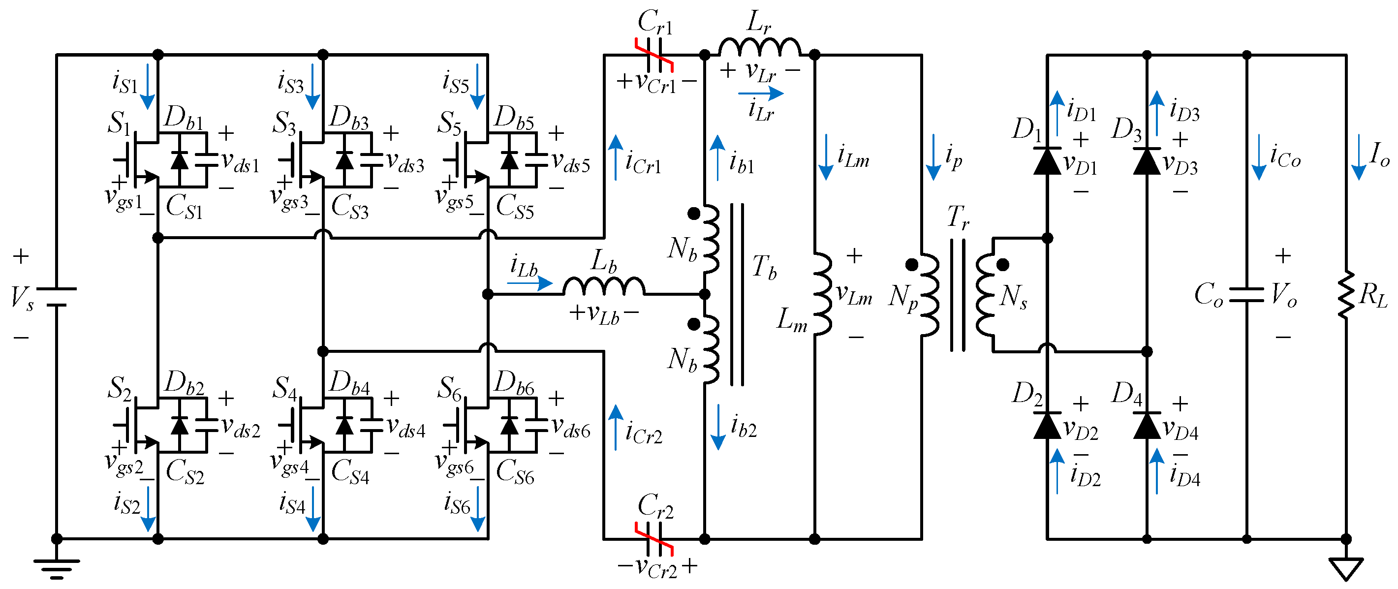
In this paper, an LLC DC-link converter based on common-mode bias variable capacitance structure is proposed, and Figure 6 shows the single-phase circuit diagram of the proposed circuit. The resonant capacitors Cr1 and Cr2 are nonlinear passive components. This paper takes the current academic literature and technical data as a starting point and further explores the nonlinear characteristics of ferroelectric dielectric ceramic capacitors for the application of an LLC resonant converter and its corresponding solutions. After that, the concept of node modularization is used for circuit layout and converter construction; the corresponding instrumentation is used for parameter and waveform measurements; and the experimental measurement data are analyzed and graphically plotted.

3.1. Operating Principle

The proposed variable-capacitance technique is based on a full-bridge LLC series resonant circuit supplemented by S5, S6, Lb, Tb, and ferroelectric resonant capacitors Cr1 and Cr2 to form a common-mode bias capacitance adjustment circuit. Figure 7 shows the corresponding equivalent circuit schematic diagram and is used to explain the operating principle of this circuit. Prior to this subsection, there are some assumptions and definitions to be given as follows:
(1)
The full-bridge output voltage is regarded as ideal and is expressed in terms of two square wave voltage sources vx and vy with a duty cycle of 50%, and vx′ and vy′ follow tightly after Cr1 and Cr2;
(2)
The center-tapped transformer Tb is viewed as ideal, and the effect of magnetizing inductance is not considered;
(3)
The center terminal of this transformer Tb is referred to as the bias node, and its potential is indicated by vb;
(4)
The values of two ferroelectric resonance capacitors Cr1 and Cr2 can be expressed as functions of their trans-voltages, namely Cr (vCr1) and Cr (vCr2), respectively;
(5)
The equivalent resistance of the output load on the primary side of the transformer is expressed as Req.
Regarding Figure 8, the common-mode voltage vcm is expressed in (6), whereas the differential-mode voltage vdm is expressed in (7):
v c m = 0.5 v x + v y
v d m = v x v y
By solving (6) and (7), the full-bridge output voltages vx and vy can be obtained:
v x = v c m + 0.5 v d m
v y = v c m 0.5 v d m
Additionally, vx, and vy with a period of Ts can be expressed as
n T s t < n + 0.5 T s                         v x = V s , v y = 0 n + 0.5 T s t < n + 1 T s v x = 0 , v y = V s
Bringing (10) into (6) and (7) yields
n T s t < n + 0.5 T s                                 v c m = 0.5 V s               ,               v d m = V s n + 0.5 T s t < n + 1 T s             v c m = 0.5 V s               ,               v d m = V s
From Figure 7, the common-mode voltage vcm′ is expressed in (12), whereas the differential-mode voltage vdm′ is expressed in (13):
v c m = 0.5 v x + v y
v d m = v x v y
Solving (14) and (15) yields
v x = v c m + 0.5 v d m
v y = v c m 0.5 v d m
Since the numbers of turns at the upper and lower terminals of the transformer Tb are Nb, the following equations can be obtained:
v x v b = v b v y
By rearranging (16), the following equation can be obtained:
v b = 0.5 v x + v y = v c m
The voltages across the ferroelectric resonant capacitors Cr1 and Cr2, called vCr1 and vCr2, respectively, are as follows:
v C r 1 = v x v x
v C r 2 = v y v y
Substituting (8) and (9) into (18) and (19) yields
v C r 1 = v c m + 0.5 v d m v c m + 0.5 v d m
v C r 2 = v c m 0.5 v d m v c m 0.5 v d m
Substituting (11) and (19) into (20) and (21) yields
v C r 1 = 0.5 v d m v d m v c m v c m = 0.5 v d m v d m v b 0.5 V s
v C r 2 = 0.5 v d m v d m + v c m v c m = 0.5 v d m v d m + v b 0.5 V s
If the amplitude of the differential-mode voltage is sufficiently small that its effect on the resonant capacitance can be neglected, the ferroelectric resonant capacitors Cr1 and Cr2 can be regarded as having the voltages of equal amplitude but opposite polarity across them. In addition, since ceramic capacitors do not have different polarities, there is no difference in capacitance regulation even if the common-mode bias is established with opposite polarities. In this case, the capacitance of resonant capacitors Cr1 and Cr2 can be expressed as a function of voltage:
v C r = v b 0.5 V s
C r 1 = C r v C r 1 C r v C r
C r 2 = C r v C r 2 C r v C r
It can be seen that the resonant capacitance can be adjusted by biasing the node potential vb, which, in turn, affects the resonant frequency and impedance. This is the core concept of common-mode bias variable-capacitance technique.
If the initial voltages of the resonant capacitors Cr1 and Cr2 are zero, (22) and (23) can be described by the corresponding currents:
v C r 1 = 0.5 v d m v d m v b 0.5 V s = i L r C r 1 d t 0.5 i L b C r 1 d t
v C r 2 = 0.5 v d m v d m + v b 0.5 V s = i L r C r 2 d t + 0.5 i L b C r 2 d t
Sequentially, the node potentials vx′ and vy′ are described by the full-bridge output voltages vx and vy and the resonant capacitor voltages vCr1 and vCr2, as shown below:
v x = v x i L r 0.5 i L b C r 1 d t
v y = v y + i L r + 0.5 i L b C r 2 d t
Bringing the voltages of the above nodes vx′ and vy′ into (17), the following equation can be obtained:
v b = 0.5 v x + v y i L r 0.5 i L b C r 1 d t + i L r + 0.5 i L b C r 2 d t
By substituting (10), (25), and (26) into (31), the voltage vb can be obtained as follows:
v b 0.5 v x + v y + i L b C r v C r d t = 0.5 V s + i L b C r v C r d t
From (32), it can be seen that the bias node potential vb is almost independent of the amplitude, frequency, and phase of the resonant tank current iLr, and its value is mainly dependent on the bias current iLb, so that the bias circuit can be analyzed independently of the resonant tank. In addition, the bias node displays a capacitive input impedance, whose reactance comes from the sum of the two resonance capacitors Cr1 and Cr2, and there is a DC voltage lift corresponding to vcm. Based on the above, the equivalent input simplified model of the bias node is shown on the right side of Figure 8.

3.2. Bias Operation Region

Considering the required bias range and the number of components, a synchronously rectified (SR) buck circuit is used to establish the bias. The equivalent circuit is shown in Figure 9, which is constructed by S5, S6, and Lb along with the simplified equivalent model of the bias node shown in Figure 8.
When the blanking time is sufficiently small, the bias node potential vb can be described by (33), where D is the duty cycle of the switch S5:
v b = V s × D
In addition, the capacitance presented by the ferroelectric MLCC is related to the magnitude of the applied bias, which can be rewritten as (34):
v C r = v b 0.5 V s = V s D 0.5
After this, Figure 10 displays the curve of bias value versus duty cycle.
As can be seen in Figure 10, the effective bias region for the synchronous-rectifier buck circuit locates between zero and 0.5Vs, and the duty cycle of 0.5 is the center of the left–right symmetry. The electric fields established between the two regions are in opposite directions but with the same field strength. Therefore, the right half of the bias region is used for capacitance control, so the minimum duty cycle of the bias circuit is 0.5 and increases with the bias value.

3.3. Ferroelectric Dielectric MLCCs

According to EIA RS-198 [38], Class-II laminated ceramic capacitors, represented by the temperature characteristics of X7R and Y5V, have a higher capacity volume density than Class-I capacitors, which is mainly due to the use of high-permittivity ferroelectric dielectrics.
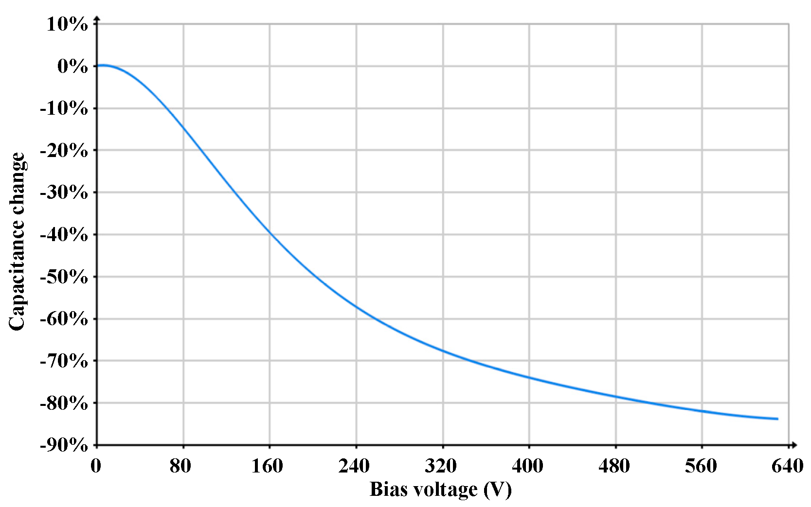
The saturation phenomenon of the ferroelectric dielectrics is similar to that of ferromagnetic materials. That is to say, such dielectrics in high field strength cause the ferroelectric polarization direction to tend mostly toward the direction of the electric field and cannot contribute to the electric flux, which is macroscopically manifested as a decrease in the relative capacitance under high field strength, as shown in Figure 11.
Thanks to the DC bias characteristics of ferro-dielectric MLCCs, they can be regarded as having variable capacitance regulated by DC bias, and their standard voltage and capacitance range are much higher than those of a typical varactor diode or a variable capacitor based on microelectromechanical technology. The common-mode bias variable capacitance mentioned herein is realized by this type of MLCC.
It is also worth noting that class II ceramic capacitors have common specifications such as X7R, X5R, and Y5V, depending on temperature characteristics. Since the proposed application is sensitive to changes in resonant capacitance and MLCCs are subject to self-driven temperature rises under circuit operation, it is preferable to select a component with a more stable capacitance over a wide temperature range. The component model GCJ31BR72J103KXJ1L is selected herein based on the capacitance bias curve provided by Murata’s design-aid website [39].

3.4. Proposed Common-Mode Bias Variable Capacitance Technique

The traditional current-equalization approach is to balance the load of each phase converter through the duty cycle control or frequency modulation of the primary side switch. This may make it difficult to achieve the ZVS condition, or each converter may be unable to maintain a fixed switching phase angle to minimize the voltage ripple. Using variable capacitors to achieve current sharing does not have the above issues. In addition, the proposed variable capacitor structure can also be applied to other types of resonant converters, such as matching the primary and secondary side resonant tank frequencies in wireless power transmission applications.
Although the proposed circuit uses an additional bias power supply, this power supply only needs to establish the voltage required to control the capacitance, and its steady-state power consumption is quite low. In addition, the common-mode bias voltage has a low correlation with the resonant tank current, making it easy to establish the control voltage. In this article, a synchronous buck circuit is used, but it depends on the voltage and power of the converter. In low-voltage systems, non-isolated power supplies such as low-voltage regulator (LDO) can also be used to establish the bias voltage.
To sum up, the proposed common-mode bias variable capacitance technique utilizes the saturation phenomenon of ferroelectric MLCC dielectrics to achieve capacitance control. Accordingly, an appropriate design to reduce the impact of common-mode node voltage ripple is necessary. This technique has some advantages, summarized below:
(1)
The bias-controlled variable capacitor technique utilizes a high-permittivity MLCC, resulting in a small size for the resonant capacitor;
(2)
The bias circuit only supplies the resonant capacitor current in the steady state, such that the power required is quite low;
(3)
The common-mode bias structure can be constructed by a non-isolated auxiliary circuit;
(4)
The voltage ripple of the bias node is small, and this is favorable for the application of the switching bias circuit;
(5)
The application of the switching technology to bias circuits can significantly extend the bias operating range;
(6)
The common-mode bias structure with the switching circuit removes the need for additional filter capacitors;
(7)
The low dependency between the bias circuit and the main circuit allows each to be regulated independently;
(8)
All the switching elements, including the bias circuit, can achieve ZVS turn-on.

4. Current-Equalization Control

4.1. Main Power Stage

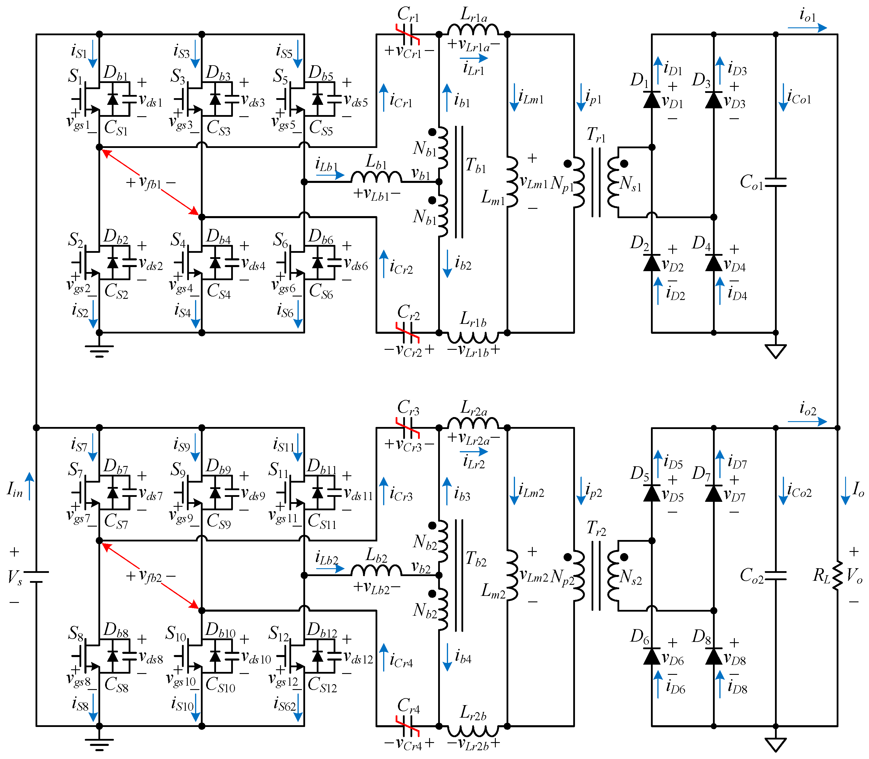
Figure 12 displays the main power stage of the experimental circuit. As for the control kernel, since the field programmable gate array (FPGA) has both sequential processing and parallel processing, while the digital signal processor (DSP) only has sequential processing; therefore, the former has better execution speed. In addition, most of the FPGA pins can also be flexibly configured, which is beneficial to applications with high input-output (IO) resource requirements, such as multi-phase, multi-sensor or multi-stage systems. Therefore, the FPGA with part number of EP3C5E144C8N is used to implement the proposed controller.

4.2. Switching Signals for Current Equalization Operation and Full-Bridge Operation

Since the output current of each phase converter cannot be known in advance of the operation of the circuit, the current-equalization controller must be able to automatically determine the operation status of the circuit and establish the required bias voltages for the resonant capacitors of each phase. The controller proposed in this paper uses the automatic master–slave current-sharing method. This controller realizes current following by locking the bias of the high-current resonant tank and boosting the bias of the low-current resonant tank to achieve phase current balancing, and the corresponding current-equalization operation is shown in Figure 13. Notably, phase shifting is realized by applying a delay time on the second phase switching signal. The delay time has been set to one-fourth of the LLC switching period (Ts) to minimize the output voltage ripple.
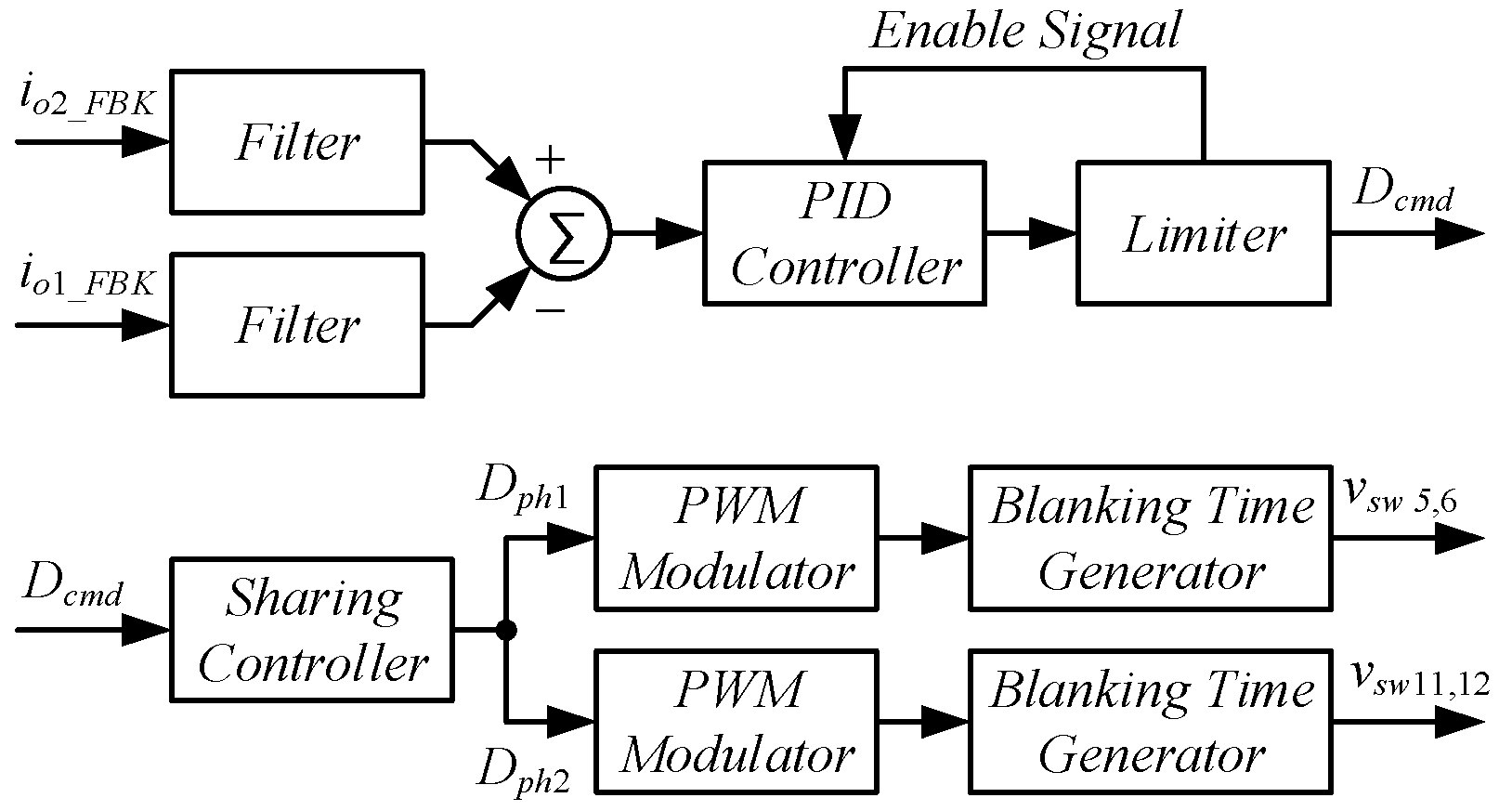
Since the LLC switching signals and regulate the output current of each phase of the converter is indispensable, Figure 14 displays how to generate the switching signals of the multi-phase LLC converter.
Figure 15 shows the flowchart of the automatic master–slave current-equalization method, whose input is the control force from the output of the PID controller and processes the duty cycle of the bias circuit. If the output of the PID module is greater than zero, the bias circuit of phase 2 is locked; hence, the duty cycle of phase 1 is increased so that the output current of phase 1 follows that of phase 2, and vice versa, where the bias circuit of phase 1 is locked and the duty cycle of phase 2 is increased so that the output current of phase 2 follows that of phase 1.
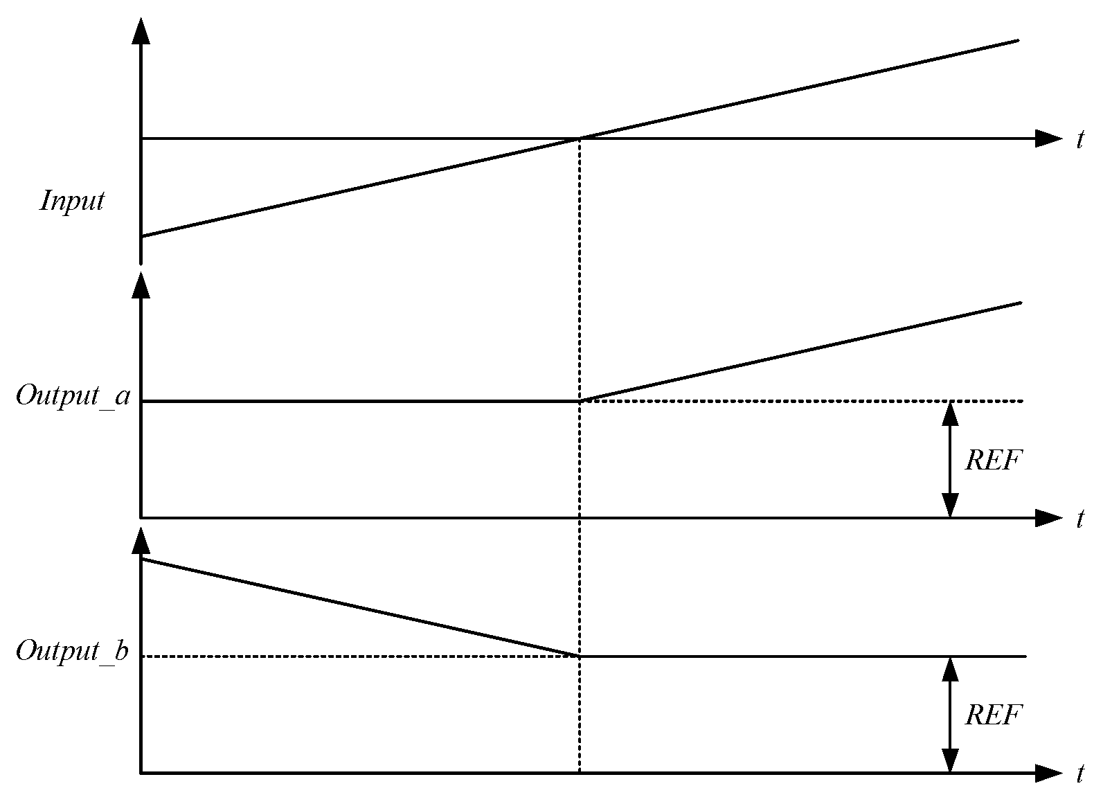
Figure 16 shows the operation flow diagram of the current-equalization control, where REF is the reference value at zero bias. When the duty cycle of the output of the bias circuit is 0.5, the amplitude of the bias voltage across Cr is zero.

5. Experimental Results and Analyses

The circuit is used to validate the proposed current-equalization technique with common-mode bias variable capacitance.

5.1. Circuit Specifications and Circuit

The experimental circuit is a two-phase LLC DC-link voltage converter with a rated power of 3.2 kW, and the corresponding circuit specifications are shown in Table 1. Figure 17 shows the prototype of the experimental circuit.

5.2. Measured Waveforms

For LLC resonant converters, if the load is too heavy, the resonance tank may enter the capacitive impedance region and lose ZVS; thus, it is necessary to verify the rated-load waveforms. For circuits such as series resonance and phase-shifted full bridge, the current under a light load may not be enough to meet the ZVS condition. Therefore, in the following, waveforms are used to confirm that the designed circuit can achieve ZVS at rated and light loads.
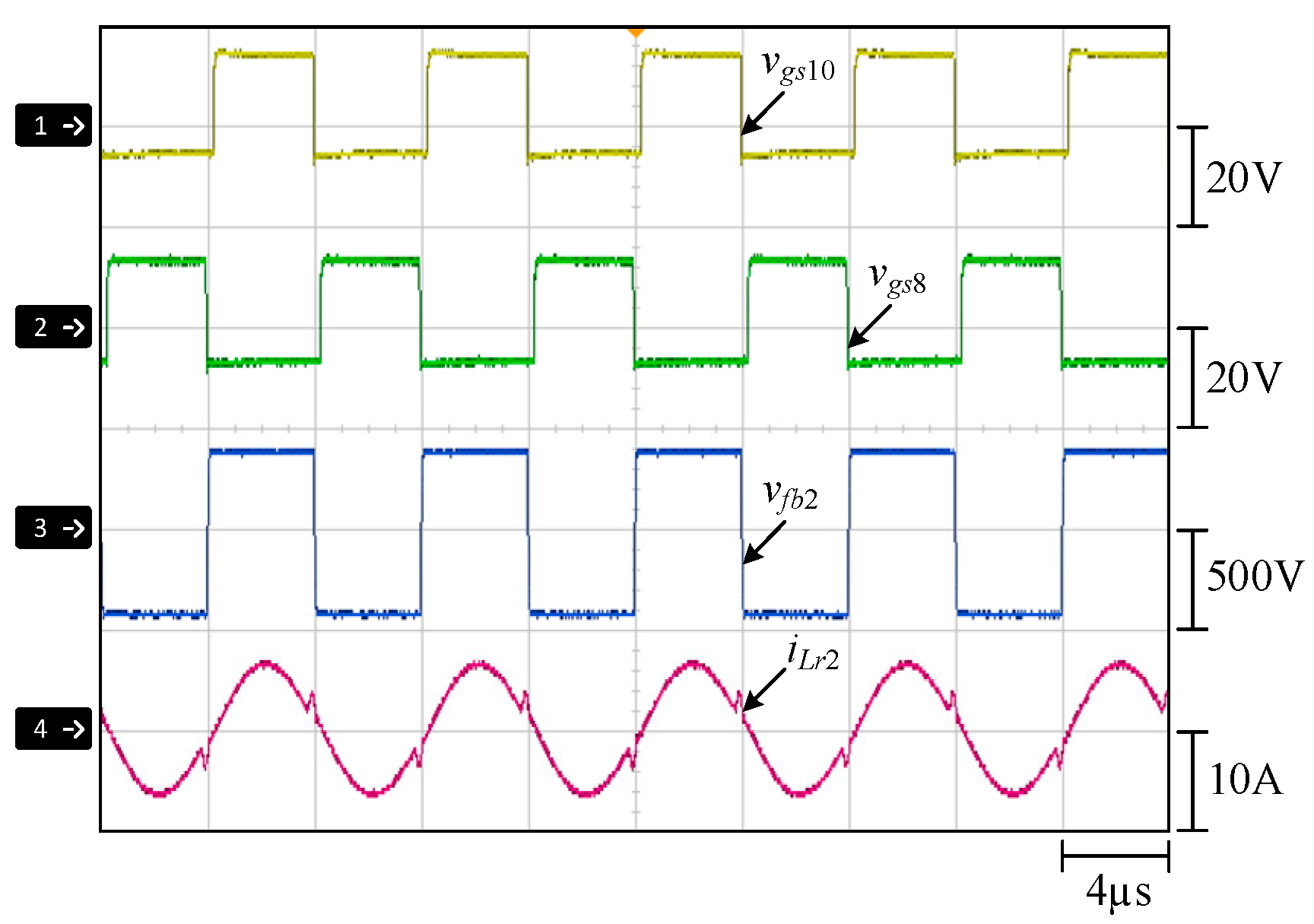
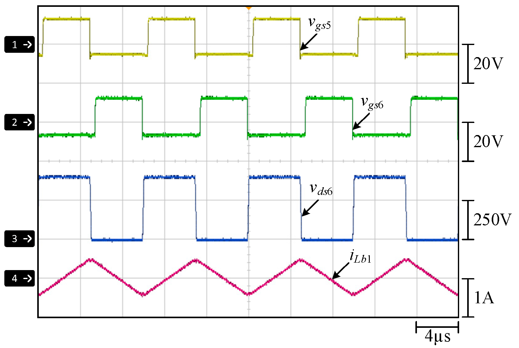
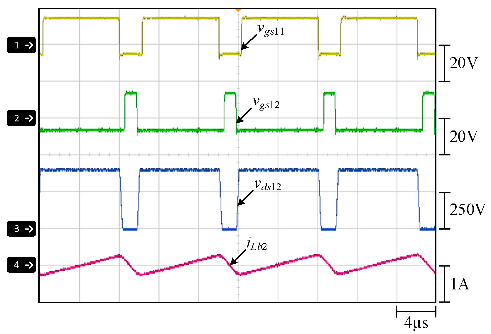
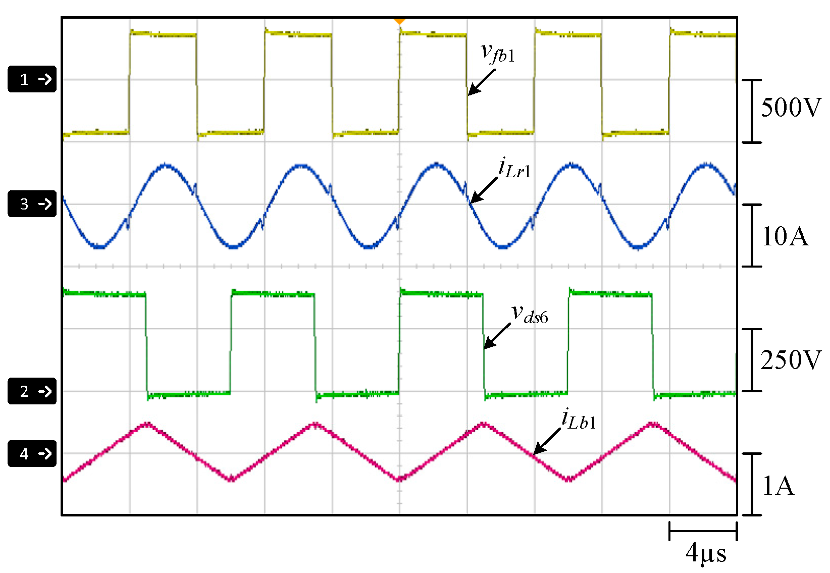
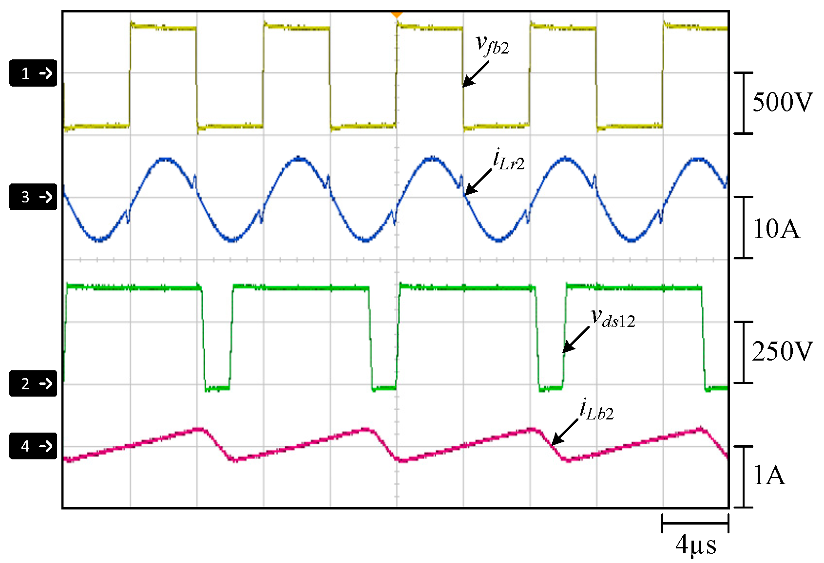
At the rated load, Figure 18 shows the measured waveforms of vgs4, vgs2, vfb1, and iLr1; Figure 19 shows the measured waveforms of vgs10, vgs8, vfb2, and iLr2; Figure 20 shows the measured waveforms of vgs5, vgs6, vds6, and iLb1; Figure 21 shows the measured waveforms of vgs11, vgs12, vds12, and iLb2. Figure 22 shows the measured waveforms of vfb1, iLr1, vds6, and iLb1; Figure 23 shows the measured waveforms of vfb2, iLr2, vds12, and iLb2.
From Figure 18, Figure 19, Figure 20, Figure 21, Figure 22 and Figure 23, it can be seen that the switching frequency of the LLC converter is 125 kHz, whereas the switching frequency of the bias circuit is 100 kHz. From the above waveforms, it can be seen that the operation of the two circuits can be maintained independently under the common use of ferroelectric MLCCs and the different switching frequencies. The main reason for this is that the common-mode bias structure only extracts the common-mode potential of the resonant capacitor, which is less correlated with the LLC resonant current, such that the volt-second balance of the bias inductance does not tend to be affected by the LLC switching frequency and the load variation. It is also worth noting that since Lr of phase 2 has a deviation of +50%, the duty cycle of this phase bias circuit is higher in order to establish the corresponding compensation bias. At the same time, the duty cycle of the phase 1 bias circuit is locked at the resonant capacitor bias, which is close to zero.
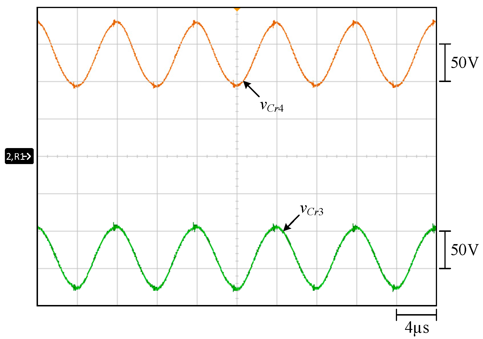
Figure 24 shows the measured waveforms vCr1 and vCr2 at rated load. Since the phase-1 resonant capacitor is not biased, the waveforms vCr1 and vCr2 are nearly coincident. For comparison convenience, Figure 25 shows the measured waveforms vCr3 and vCr4 at rated load. In order to compensate for the load current deviation, the phase-2 bias circuit establishes a resonant capacitor bias voltage of 128.3 V. The bias voltage is negative for Cr3 and positive for Cr4; thus, the voltage waveforms of the two capacitors do not coincide.
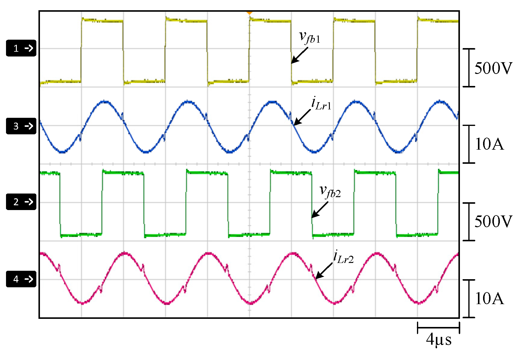
Figure 26 shows the measured waveforms vfb1, iLr1, vfb2, and iLr2 at rated load. The phase difference between phase 1 and phase 2 is maintained at 90° in order to maintain the advantage of lower ripple of the output voltage of the multiphase LLC converter.
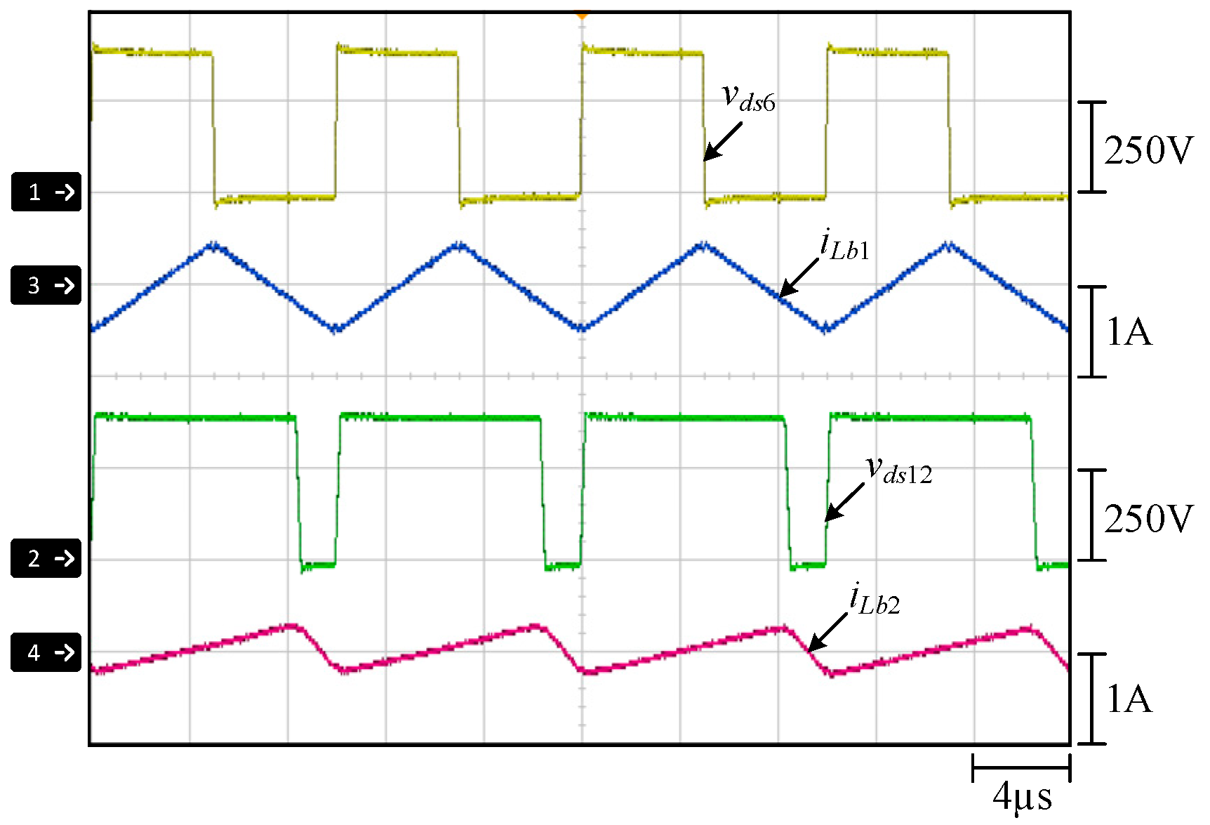
Figure 27 shows the measured waveforms vds6, iLb1, vds12, and iLb2 at rated load. In this case, the duty cycle of phase-2 bias circuit is 0.81, whereas the duty cycle of phase 1 bias circuit is locked at 0.5.
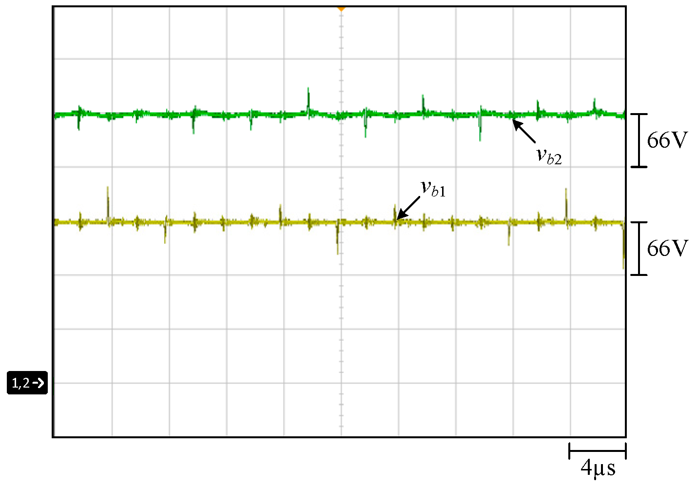
Figure 28 shows the measured waveforms vb1 and vb2 at rated load. In this case, the phase-2 bias node potential vb2 is 328.9 V, whereas the phase 1 bias node potential vb1 is locked at 200 V.
Figure 29 shows the measured waveforms io1 and io2 at rated load. There is a ripple in the output current of each phase that is twice the switching frequency of the LLC circuit, and the phase difference between the two rectifier output currents is 180°.
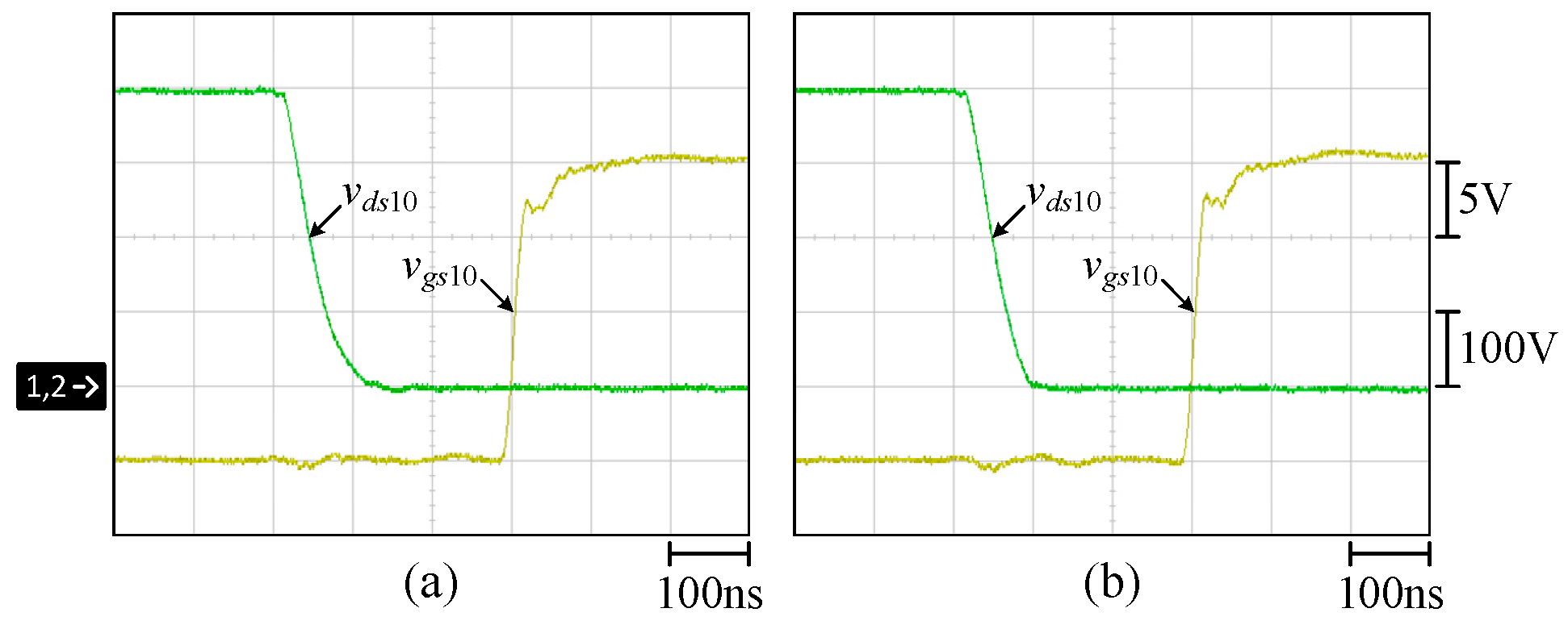
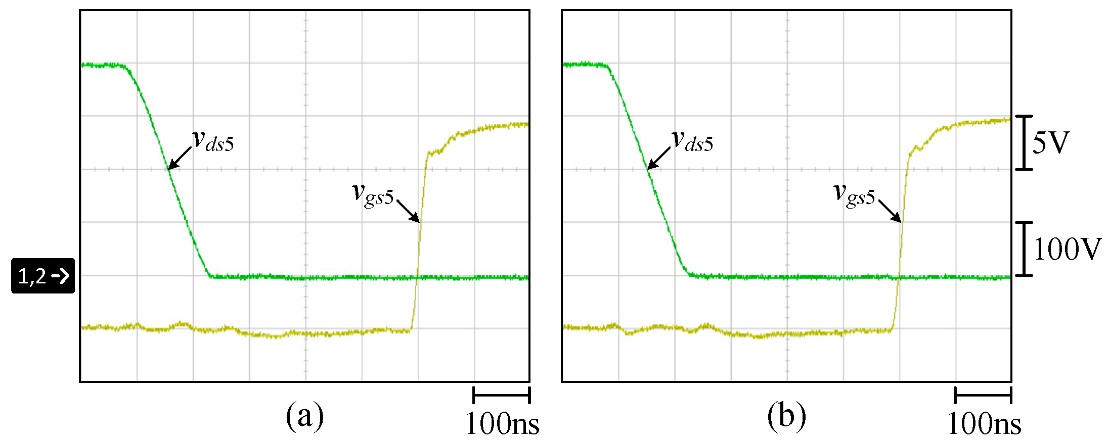
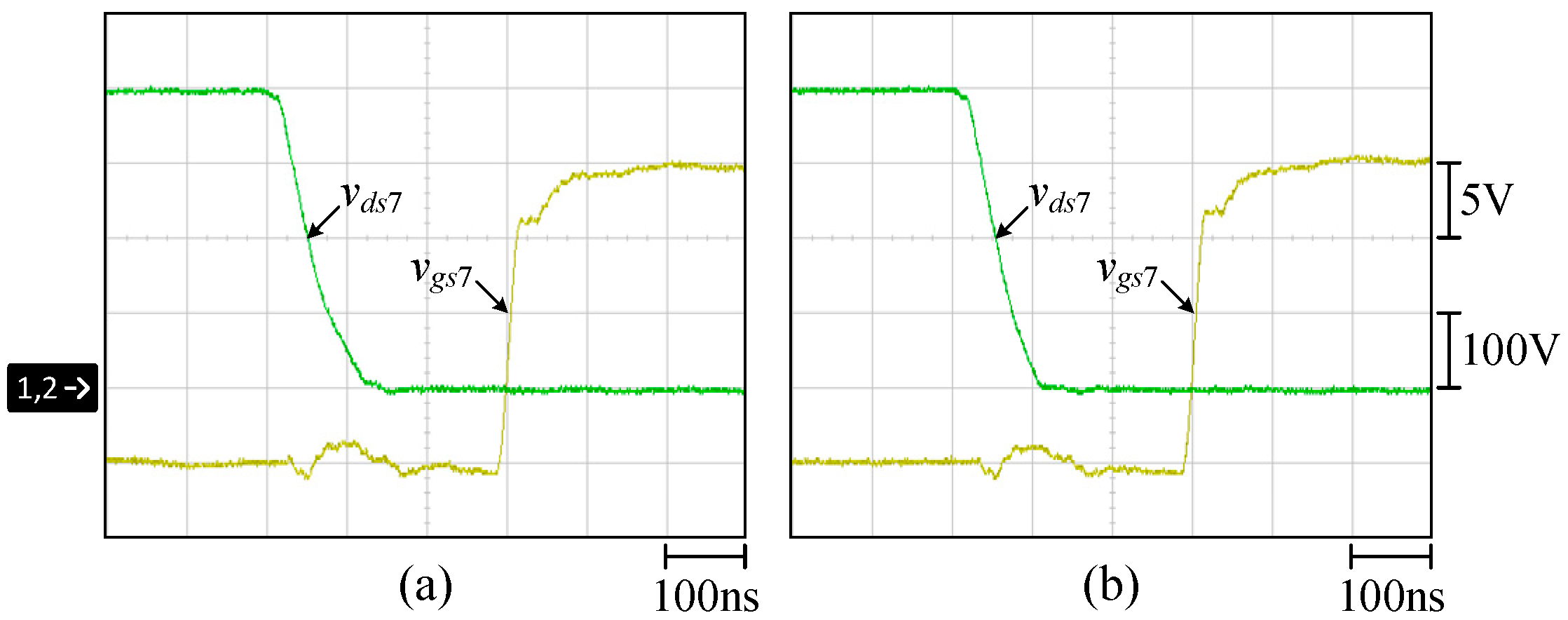
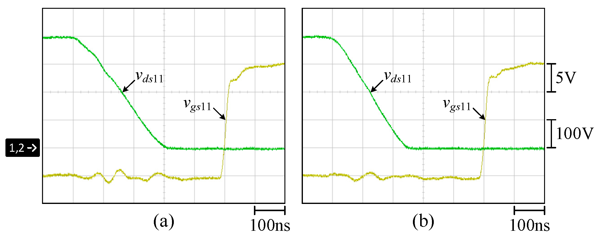
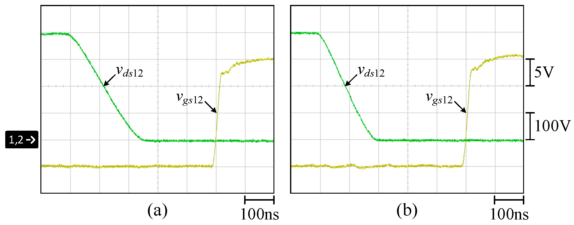
Figure 30, Figure 31, Figure 32, Figure 33, Figure 34, Figure 35, Figure 36, Figure 37, Figure 38, Figure 39, Figure 40 and Figure 41 show the waveforms relevant to the switches S1 to S12. All the switches of the proposed circuit can realize ZVS turn-on at 100% load and 10% load.

5.3. Current Error Measurement

The main purpose of this experiment is to measure the phase current difference between disabling current-equalization control and enabling current-equalization control when there is an inductance deviation in the resonance tank, and is to verify the feasibility of the proposed technique for current equalization.
The experimental setup is a two-phase LLC resonant converter, and the current error ratio is shown below:
e r r o r = i 1 0.5 i 1 + i 2 0.5 i 1 + i 2 × 100 % = i 2 0.5 i 1 + i 2 0.5 i 1 + i 2 × 100 % = i 1 i 2 i 1 + i 2 × 100 %
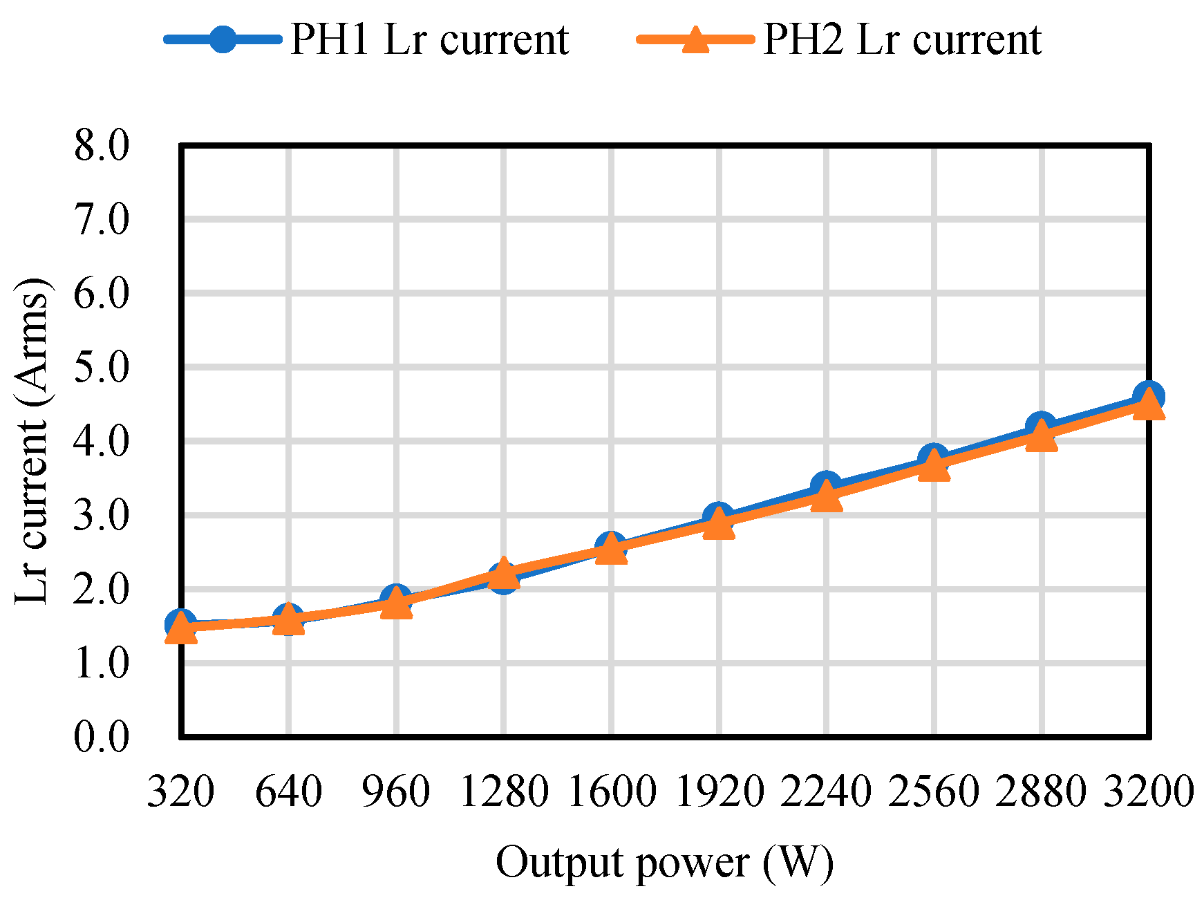
Figure 42 shows the resonant current curves of each phase circuit at different loads without the current-equalization control enabled, and the resonant capacitor bias of each phase circuit is locked at 0 V. The magnetizing current is the main component of the resonant current at 10% load, such that there is no significant difference between phases, but as the load increases, the resonant current of phase 1 will be higher than that of phase 2, which is the most important component of the resonant current.
Figure 43 shows the resonant current curves of each phase circuit at different loads when current-equalization control is enabled; the resonant capacitor bias voltage of each phase circuit is regulated by the current-equalization controller.
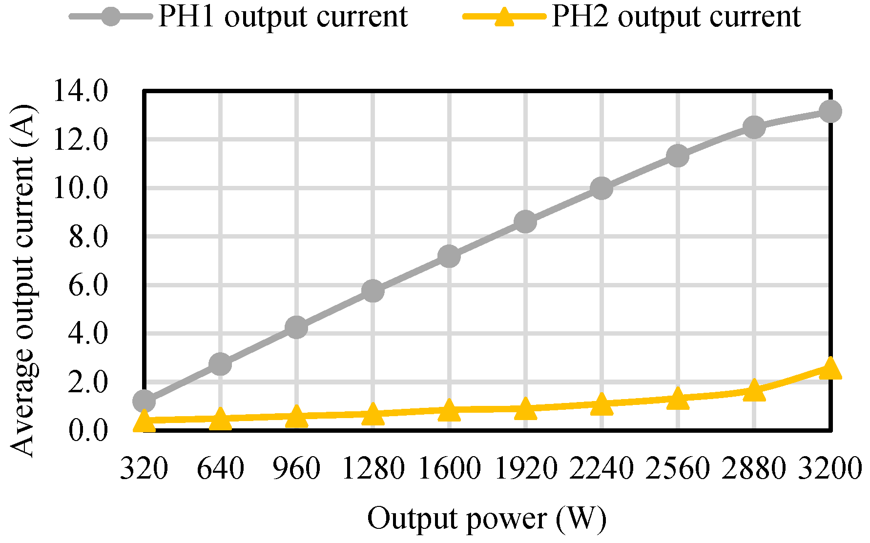
Figure 44 shows the average output current curves of each phase circuit at different loads without current-equalization control enabled, such that the resonant capacitor bias voltage of each phase circuit is locked at 0 V. From this figure, it can be seen that the average output current of phase 1 is significantly higher than that of phase 2 under each load.
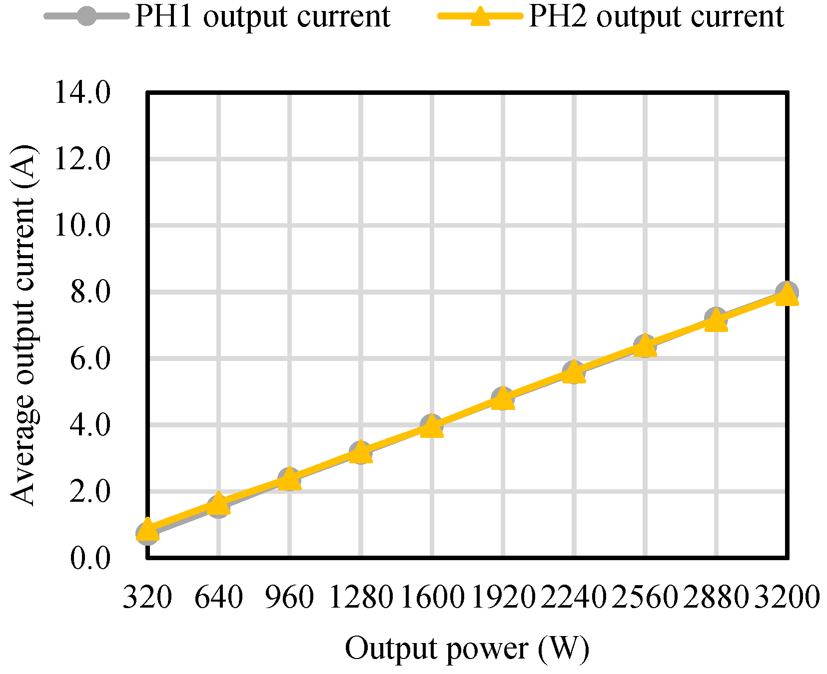
Figure 45 shows the output current curves of each phase circuit at different loads when current-equalization control is enabled, and the resonant capacitor bias voltage of each phase circuit is regulated by the current-equalization controller such that the average output current is almost the same.
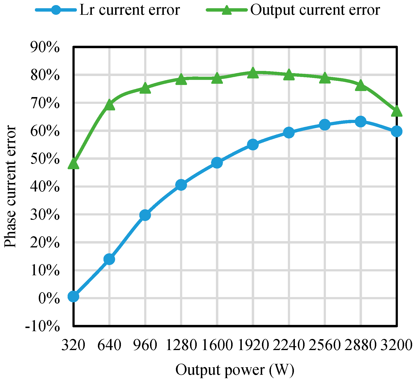
Figure 46 shows the curves of the current error rate of each phase circuit at different loads without current-equalization control, and the resonant capacitor bias voltage of each phase circuit is locked at 0 V during this time. From this figure, it can be found that there is a very high current error rate for the output current.
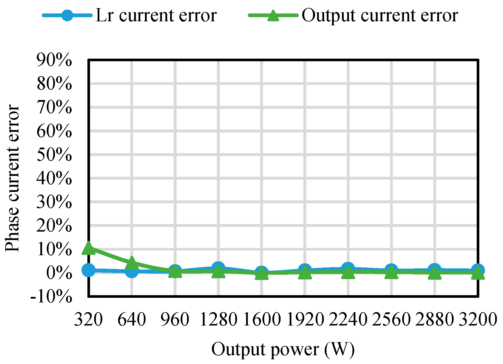
Figure 47 shows the current error rate curve of each phase circuit under different loads when the current-equalization control is enabled, and the resonant capacitor bias voltage of each phase circuit is regulated by the current-equalization controller during this time. From this figure, it can be found that there is a high error rate for the output current at light load, which is mainly caused by the linearity deviation of the ADC and the current meter, but the error will be reduced rapidly with an increase in the load.

5.4. Measurement of Efficiency and DC Gain

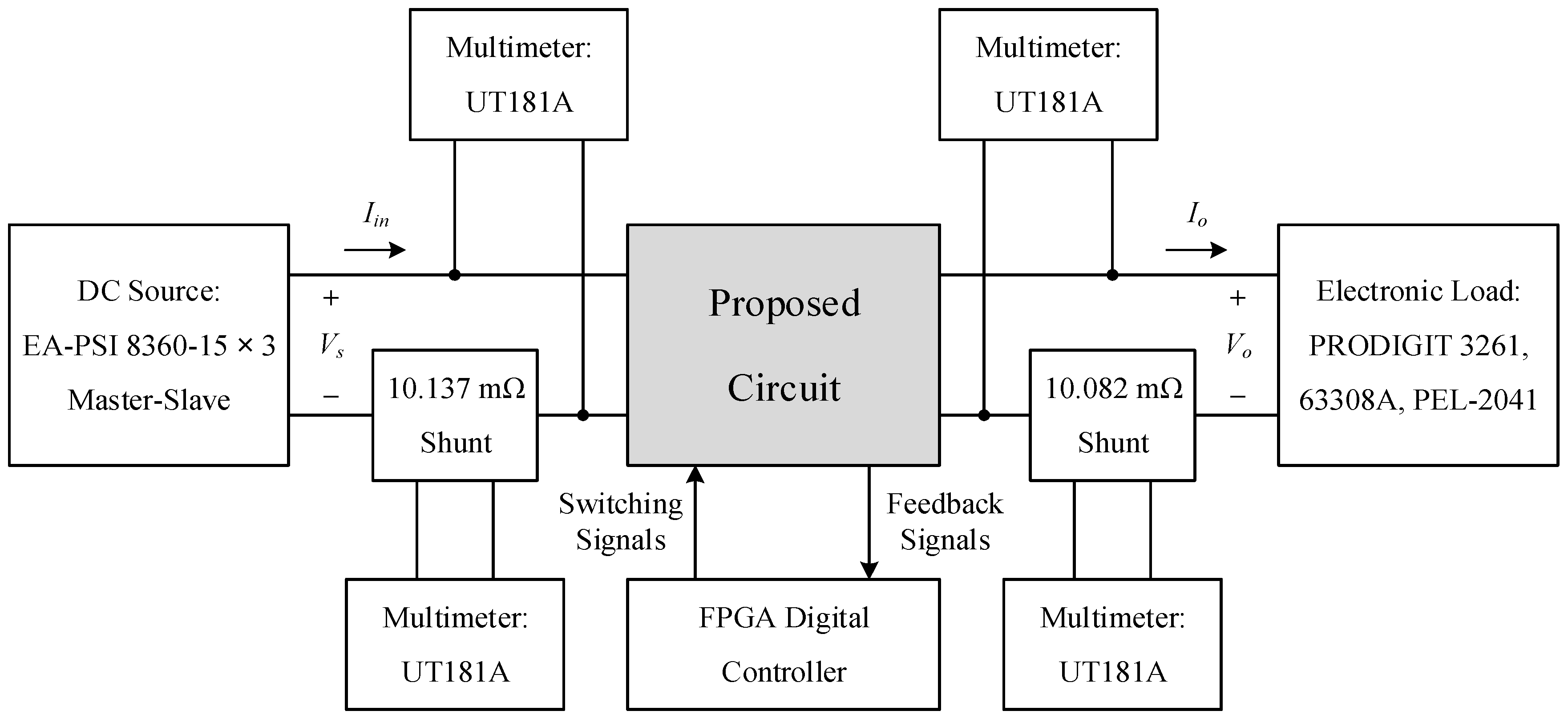
How to measure the efficiency and DC gain of the proposed circuit is shown schematically in Figure 48, where a temperature-stable Constantan alloy current sampling resistor (Shunt) is used, and the actual resistance is confirmed by a micro-ohmmeter—specifically, a GOM-805—for the measurements. Due to the small percentage of power loss in the proposed circuit, a small measurement error is enough to affect the efficiency curve. Therefore, this experiment requires the converter to be properly warmed up before the experiment, and more than 10 min should be allowed between measurement points to achieve thermal balance of the components. In addition, in order to further minimize the random error, 10 samples are averaged for each measurement point. By the way, in Figure 48, three DC sources, named EA-PSI 8360-15, which are manufactured by EA ELEKTRO-AUTOMATIK, Viersen, Germany, and an electronic load, named PRODIGIT 3261, which is manufactured by PRODIGIT ELECTRONICS, New Taipei City, Taiwan.
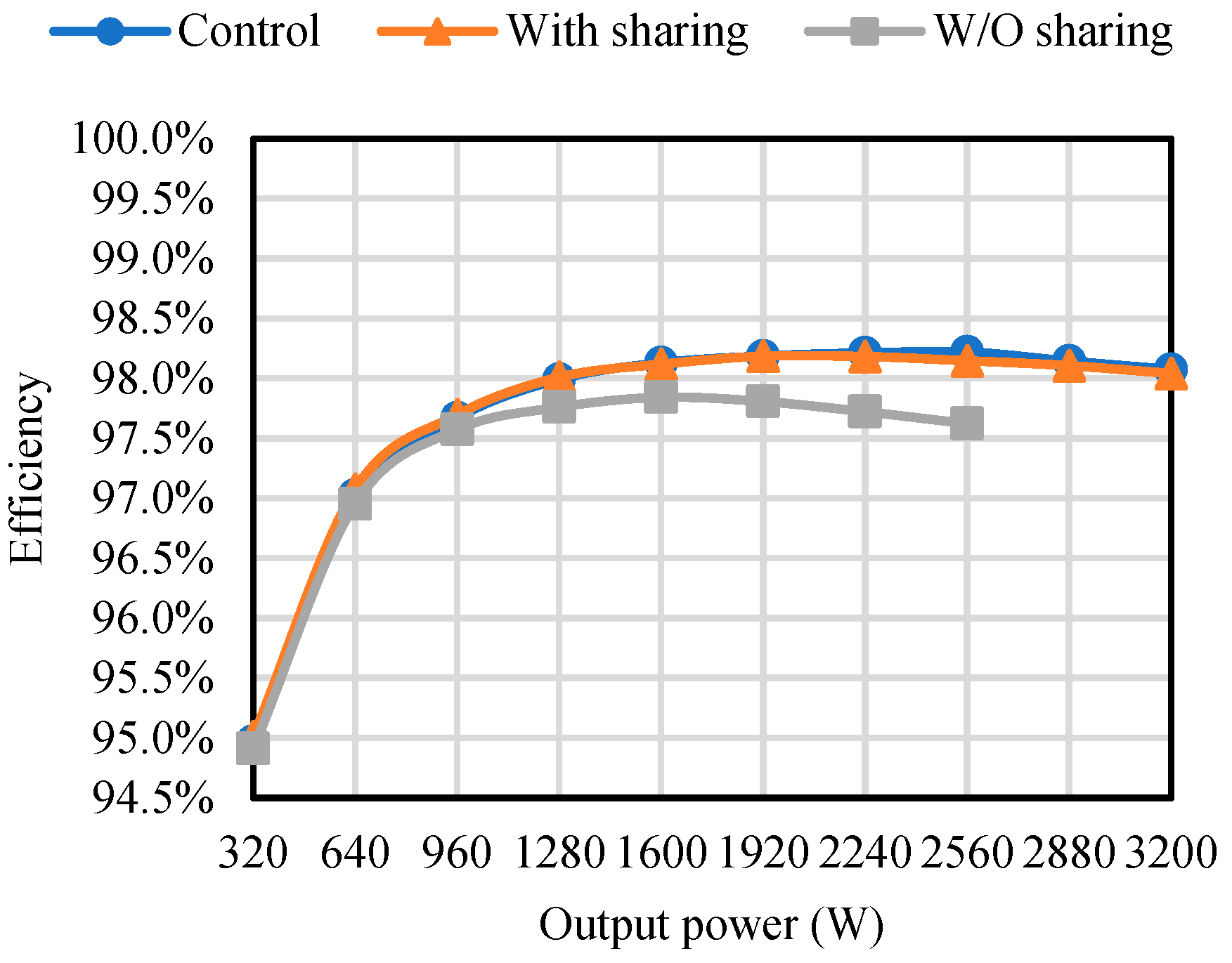
The purpose of this measurement is to record the DC gain and efficiency of the proposed circuit under each experimental condition. In order to evaluate the effect of resonant inductance deviation on the proposed circuit, the measurement items include a control group with 0% Lr deviation (labeled in the figure: Control), and a current-equalization experimental group with +50% Lr deviation (labeled in the figure: With sharing). In addition, the load imbalance will have a negative effect on the efficiency, which is verified by an experimental group with +50% Lr deviation and without current-equalization control (labeled in the figure: W/O sharing).
Figure 49 shows the curves of efficiency versus output power in three groups, comprising “Control”, “With sharing”, and “W/O sharing”. The first and second groups have very close efficiency curves, and both of them have a power conversion efficiency higher than 98% at half load. In addition, the measured data show that the difference in efficiency between these two groups is within 0.07% for all output powers, and this confirms that the proposed equalization technique can compensate for the phase current imbalance caused by the 0~50% Lr deviation without significantly affecting the efficiency.
In addition, the efficiency of the third group is significantly lower than the other two groups. The main reason is that phase 1 carries most of the load current, which leads to a drastic increase in the equivalent series resistance (ESR) losses of the capacitors in this phase, and at the same time, there is still iron loss in the transformer of phase 2, which leads to an increase in the total loss of the circuit. However, most of the losses occur in the phase 1 circuit under this operating condition. Consequently, the efficiency is measured up to 80% of the rated output power in order to avoid overheating of the circuit components.
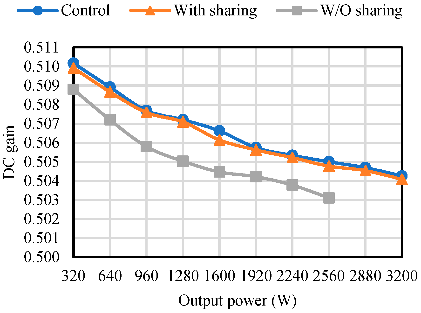
Figure 50 shows the curves of DC gain versus output power in the three groups. The DC gain at each output power is larger than 0.5 because the switching frequency f s = 125   kHz is lower than the resonant frequency f r = 130   kHz . The DC gain of the experimental circuit meets the design specification of 0.5 ± 3 % under all operating conditions.
Moreover, the DC gain increase as the output power decreases. This is mainly because under different values of the output power, the different values of the quality factor Q of the resonant tank and the different values of the voltage drop of the equivalent impedance of the resonant tank. At the same time, a lower Q value means a higher voltage gain. Compared to the first group, the gain of the second group is slightly lower, which is also due to the fact that phase 2 is subjected to an additional resonant inductance, resulting in an increase in the values of Q and equivalent impedance of the resonant tank. Therefore, the same phenomenon also exists in the unbalanced experimental set with +50% Lr deviation (labeled in the figure: W/O sharing). Since most of the load current is supplied by phase 1 without current equalization enabled, the value of Q of this phase rises further and the equivalent impedance loss increases dramatically, and so its DC gain is lower than those of the control group and current-equalization experimental group.

6. Comparison of Related Literature

Table 2 shows a comparison between the existing circuits and the proposed circuit, classified into four methods with seven items to be compared, comprising extendibility, phase shift switching, phase shielding ability, active current control, auxiliary circuit power level, auxiliary circuit power losses, current error ratio, and peak efficiency.

7. Conclusions

In this paper, a variable-capacitance current-equalization technique based on ferroelectric dielectric MLCCs is presented to balance the load current of each phase of an LLC converter by adjusting the resonant capacitance through the proposed common-mode bias structure and switching auxiliary circuit. The capacitance of ferroelectric materials is related to the strength of the electric field. Since an MLCC’s capacitance using such dielectrics decreases with an increase in the voltage across it, the proposed circuit utilizes this phenomenon to achieve resonant capacitance regulation. Therefore, a new bias structure in terms of common-mode potential is presented, where the resonant capacitor bias is equivalent to the common-mode potential difference between the full-bridge node and the primary side of the transformer. Since the common-mode potential difference of the proposed circuit is mainly a DC value, it is suitable for use with a non-isolated switching bias circuit, and the output capacitor of the bias circuit can be shared with the LLC resonant capacitor without the need for additional capacitors. Since the switching bias circuit only needs to build up the MLCC bias and the switching elements are capable of ZVS turn-on, the losses are very low. The efficiency is over 98% above half-load, while the current error rate of each phase with current-equalization control enabled is quite low within 1% except under a light load. In the future, the component loss and temperature rise of the MLCC will be investigated.

Author Contributions

Conceptualization, Y.-L.L. and K.-I.H.; methodology, Y.-L.L. and K.-I.H.; software, Y.-L.L.; validation, Y.-L.L. and K.-I.H.; formal analysis, Y.-L.L. and K.-I.H.; investigation, Y.-L.L.; resources, Y.-L.L.; data curation, Y.-L.L.; writing—original draft preparation, Y.-L.L. and K.-I.H.; writing—review and editing, K.-I.H.; visualization, Y.-L.L.; supervision, K.-I.H.; project administration, K.-I.H.; funding acquisition, K.-I.H. All authors have read and agreed to the published version of the manuscript.

Funding

This research was funded by the Ministry of Science and Technology, Taiwan, under Grant Number NSTC 112-2221-E-027-015-MY2.

Data Availability Statement

No new data were created or analyzed in this study. Data sharing is not applicable to this article.

Conflicts of Interest

Author Yue-Lin Lee was employed by the company Delta Electronics Inc. The remaining authors declare that the research was conducted in the absence of any commercial or financial relationships that could be construed as a potential conflict of interest.

References

  1. Baba, D. Benefits of a Multiphase Buck Converter. Texas Instruments. 2012. Available online: https://www.ti.com/lit/an/slyt449/slyt449.pdf?ts=1652769828584&ref_url=https%253A%252F%252Fwww.google.com%252F (accessed on 5 February 2023).
  2. Wang, H.; Chen, Y.; Qiu, Y.; Fang, P.; Zhang, Y.; Wang, L.; Liu, Y.-F.; Afsharian, J.; Yang, Z. Common capacitor multiphase LLC converter with passive current sharing ability. IEEE Trans. Power Electron. 2018, 33, 370–387. [Google Scholar] [CrossRef]
  3. Wang, H.; Chen, Y.; Liu, Y.-F.; Afsharian, J.; Yang, Z. A passive current sharing method with common inductor multiphase LLC resonant converter. IEEE Trans. Power Electron. 2017, 32, 6994–7010. [Google Scholar] [CrossRef]
  4. Li, Y.; Shao, S.; Chen, H.; Zhang, J.; Sheng, K. High-gain high-efficiency IPOS LLC converter with coupled transformer and current sharing capability. IEEE CPSS Trans. Power Electron. Appl. 2020, 5, 63–73. [Google Scholar] [CrossRef]
  5. Yang, Y.; Yao, J.; Li, H.; Zhao, J. A novel current sharing method by grouping transformer’s secondary windings for a multiphase LLC resonant converter. IEEE Trans. Power Electron. 2020, 35, 4877–4890. [Google Scholar] [CrossRef]
  6. Ahmad, U.; Cha, H.; Naseem, N. Integrated current balancing transformer based input-parallel output-parallel LLC resonant converter modules. IEEE Trans. Power Electron. 2021, 36, 5278–5289. [Google Scholar]
  7. Kirshenboim, O.; Peretz, M. Combined multilevel and two-phase interleaved LLC converter with enhanced power processing characteristics and natural current sharing. IEEE Trans. Power Electron. 2018, 33, 5613–5620. [Google Scholar] [CrossRef]
  8. Shimada, T. Current sharing method using secondary voltage ripple for an interleaved LLC resonant converter. In Proceedings of the 2019 IEEE Conference on Power Electronics and Applications, Elazig, Turkey, 25–27 September 2019; pp. 1–7. [Google Scholar]
  9. Noah, M.; Endo, S.; Ishibashi, H.; Nanamori, K.; Imaoka, J.; Umetani, K.; Yamamoto, M. A current sharing method utilizing single balancing transformer for a multiphase LLC resonant converter with integrated magnetic. IEEE J. Emerg. Sel. Top. Power Electron. 2018, 6, 977–992. [Google Scholar] [CrossRef]
  10. Nakakohara, Y.; Otake, H.; Evans, T.; Tomohiko, M.; Tsuruya, M.; Nakahara, K. Three-phase LLC series resonant dc/dc converter using sic mosfets to realize high-voltage and high-frequency operation. IEEE Trans. Ind. Electron. 2016, 63, 2103–2110. [Google Scholar] [CrossRef]
  11. “3kW Dual-Phase LLC Evaluation Board.” Infineon. Available online: https://www.infineon.com/cms/en/product/evaluation-boards/eval_3kw_2llc_c7_20/ (accessed on 24 February 2023).
  12. Murata, K.; Kurokawa, F. An interleaved PFM LLC resonant converter with phase-shift compensation. IEEE Trans. Power Electron. 2016, 31, 2264–2272. [Google Scholar] [CrossRef]
  13. Arshadi, S.A.; Ordonez, M.; Eberle, W.; Saket, M.A.; Craciun, M.; Botting, C. Unbalanced three-phase LLC resonant converters: Analysis and trigonometric current balancing. IEEE Trans. Power Electron. 2019, 34, 2025–2038. [Google Scholar] [CrossRef]
  14. Two-Phase Interleaved LLC Resonant Converter Design with C2000TM Microcontrollers; Texas Instruments: Dallas, TX, USA, 2020; Available online: https://www.ti.com/lit/ug/tiduct9a/tiduct9a.pdf?ts=1652705048373&ref_url=https%253A%252F%252Fwww.ti.com%252Ftool%252FTIDM-1001 (accessed on 1 March 2023).
  15. Liu, F.; Zhou, R.G.X.; Ji, S.; Zhao, Q.; Zhang, X. An input-series-output-parallel converter system exhibiting natural input-voltage sharing and output-current sharing. IEEE Trans. Ind. Electron. 2021, 68, 1166–1177. [Google Scholar] [CrossRef]
  16. Chen, H.; Wu, X.; Shao, S. A current-sharing method for interleaved high-frequency LLC converter with partial energy processing. IEEE Trans. Ind. Electron. 2020, 67, 1498–1507. [Google Scholar] [CrossRef]
  17. Wang, M.; Zha, X.; Pan, S.; Gong, J.; Lin, W. A current-sharing method for interleaved high-frequency LLC converter with partial energy phase shift regulation. IEEE J. Emerg. Sel. Top. Power Electron. 2022, 10, 760–772. [Google Scholar] [CrossRef]
  18. Orietti, E.; Mattavelli, P.; Spiazzi, G.; Adragna, C.; Gattavari, G. Two-phase interleaved LLC resonant converter with current-controlled inductor. In Proceedings of the 2009 IEEE Brazilian Power Electronics Conference (BPEC), Bonito-Mato Grosso do Sul, Brazil, 27 September–1 October 2009; pp. 298–304. [Google Scholar]
  19. Hu, Z.; Qiu, Y.; Liu, Y.-F.; Sen, P.C. A control strategy and design method for interleaved LLC converters operating at variable switching frequency. IEEE Trans. Power Electron. 2014, 29, 4426–4437. [Google Scholar] [CrossRef]
  20. Thenathayalan, D.; Park, J. Highly flexible high-efficiency multiple-resonant wireless power transfer system using a controllable inductor. IEEE J. Emerg. Sel. Top. Power Electron. 2019, 7, 1914–1930. [Google Scholar] [CrossRef]
  21. Assadsangabi, B.; Mohamed Al, M.S.; Takahata, K. Planar variable inductor controlled by ferrofluid actuation. IEEE Trans. Magn. 2013, 49, 1402–1406. [Google Scholar] [CrossRef]
  22. Hu, Y.; Huber, L.; Jovanovic, M.M. Single-stage, universal-input ac/dc LED driver with current-controlled variable PFC boost inductor. IEEE Trans. Power Electron. 2012, 27, 1579–1588. [Google Scholar]
  23. Martins, M.; Perdigao, M.S.; Mendes, A.M.S.; Pinto, R.A.; Alonso, J.M. Analysis, design, and experimentation of a dimmable resonant-switched-capacitor LED driver with variable inductor control. IEEE Trans. Power Electron. 2017, 32, 3051–3062. [Google Scholar] [CrossRef]
  24. Alonso, J.M.M.; Perdigao, S.; Vaquero, D.G.; Calleja, A.J.; Saraiva, E.S. Analysis, design, and experimentation on constant-frequency dc-dc resonant converters with magnetic control. IEEE Trans. Power Electron. 2012, 27, 1369–1382. [Google Scholar] [CrossRef]
  25. Wei, Y.; Luo, Q.X.; Du, A.N.; Alonso, J.M.; Mantooth, H.A. Analysis and design of the LLC resonant converter with variable inductor control based on time-domain analysis. IEEE Trans. Ind. Electron. 2020, 67, 5432–5443. [Google Scholar] [CrossRef]
  26. Wei, Y.; Woldegiorgis, D.; Mantooth, A. Variable resonant and magnetizing inductor control for LLC resonant converter. In Proceedings of the 2020 IEEE International Symposium on Power Electronics for Distributed Generation Systems (PEDG), Dubrovnik, Croatia, 28 September–1 October 2020; pp. 149–153. [Google Scholar]
  27. Xu, G.; Koyama, Y.; Sogabe, Y.; Amemiya, N. Current sharing in spiral copper-plated multifilament coated conductors. IEEE Trans. Appl. Supercond. 2024, 34, 1–5. [Google Scholar] [CrossRef]
  28. Baek, D.-H.; Eun, Y.; Kwon, D.-S.; Kim, M.-O.; Chung, T.; Kim, J. Widely tunable variable capacitor with switching and latching mechanisms. IEEE Electron Device Lett. 2015, 36, 186–188. [Google Scholar] [CrossRef]
  29. Yang, H.-H.; Han, C.-H.; Choi, S.-J.; Choi, D.-H.; Yoon, J.-B. Signal power-insensitive analog mems tunable capacitor by immobilizing the movable plates. IEEE J. Microelectromech. Syst. 2015, 24, 1545–1556. [Google Scholar] [CrossRef]
  30. Patel, C.D.; Rebeiz, G.M. High-Q 3 b/4 b RF MEMS digitally tunable capacitors for 0.8–3 GHz applications. IEEE Microw. Wirel. Compon. Lett. 2012, 22, 394–396. [Google Scholar] [CrossRef]
  31. Gu, L.; Li, X. Rotational driven RF variable capacitors with post-CMOS processes. IEEE Electron Device Lett. 2008, 29, 195–197. [Google Scholar] [CrossRef]
  32. Yeh, J.A.; Chang, C.A.; Cheng, C.-C.; Huang, J.-Y.; Hsu, S.S.H. Microwave characteristics of liquid-crystal tunable capacitors. IEEE Electron Device Lett. 2005, 26, 451–453. [Google Scholar] [CrossRef]
  33. Harada, K.; Katsuki, A.M.; Fujiwara, N.H.; Matsushita, H. Resonant converter controlled by variable capacitance devices. IEEE Trans. Power Electron. 1993, 8, 404–410. [Google Scholar] [CrossRef]
  34. Ben-Yaakov, S. Characterization of ferroelectric ceramic capacitors. In Proceedings of the 2018 IEEE European Conference on Power Electronics and Applications (EPE ECCE Europe), Riga, Latvia, 17–21 September 2018; pp. 1–8. [Google Scholar]
  35. Tian, J.; Hu, A.P. A dc-voltage-controlled variable capacitor for stabilizing the ZVS frequency of a resonant converter for wireless power transfer. IEEE Trans. Power Electron. 2017, 32, 2312–2318. [Google Scholar] [CrossRef]
  36. Tishechkin, S.; Ben-Yaakov, S. Adaptive capacitance impedance matching (ACIM) of WPT systems by voltage controlled capacitors. In Proceedings of the 2019 IEEE PELS Workshop on Emerging Technologies: Wireless Power Transfer (WoW), London, UK, 18–21 June 2019; pp. 396–400. [Google Scholar]
  37. Zeng, H.; Peng, F.Z. Non-linear capacitor based variable capacitor for self-tuning resonant converter in wireless power transfer. In Proceedings of the 2018 IEEE Applied Power Electronics Conference and Exposition (APEC), San Antonio, TX, USA, 4–8 March 2018; pp. 1375–1379. [Google Scholar]
  38. EIA STANDARD, RS-198-B; Ceramic Dielectric Capacitors 1, 2 and 3. Engineering Department, Electronics Inmstitutes Association: Washington, DC, USA, 1971.
  39. “Design Support Software Simsurfing”. muRata: Kyoto, Japan, 2019. Available online: https://www.murata.com/en-us/tool/simsurfing (accessed on 3 March 2023).
Figure 1. Domestic low-voltage DC power supply system structure.
Energies 17 02793 g001
Figure 2. Current equalization strategy of a multiphase resonant converter.
Energies 17 02793 g002
Figure 3. Typical common-mode bias variable capacitance structure.
Energies 17 02793 g003
Figure 4. FHA model of the LLC resonant converter.
Energies 17 02793 g004
Figure 5. Relationship among voltage gain, resonant capacitance, and resonant inductance at (a) RL = 25 Ω; (b) RL = 250 Ω.
Energies 17 02793 g005
Figure 6. Circuit diagram of single-phase LLC converter with variable capacitance technique.
Energies 17 02793 g006
Figure 7. Equivalent model of the proposed common-mode bias circuit.
Energies 17 02793 g007
Figure 8. Simplified equivalent model of the bias node.
Energies 17 02793 g008
Figure 9. Equivalent bias circuit.
Energies 17 02793 g009
Figure 10. Curve of bias value versus duty cycle.
Energies 17 02793 g010
Figure 11. Curve of capacitance change versus bias voltage.
Energies 17 02793 g011
Figure 12. Circuit diagram having four capacitors with common-mode bias variable capacitance used.
Energies 17 02793 g012
Figure 13. Switching signals for current-equalization operation.
Energies 17 02793 g013
Figure 14. Switching signals for full-bridge operation.
Energies 17 02793 g014
Figure 15. Flowchart of the current-equalization control.
Energies 17 02793 g015
Figure 16. Input and output schematic of current-equalization control.
Energies 17 02793 g016
Figure 17. Experimental setup.
Energies 17 02793 g017
Figure 18. Measured waveforms at rated load: (1) vgs4; (2) vgs2; (3) vfb1; (4) iLr1.
Energies 17 02793 g018
Figure 19. Measured waveforms at rated load: (1) vgs10; (2) vgs8; (3) vfb2; (4) iLr2.
Energies 17 02793 g019
Figure 20. Measured waveforms at rated load: (1) vgs5; (2) vgs6; (3) vds6; (4) iLb1.
Energies 17 02793 g020
Figure 21. Measured waveforms at rated load: (1) vgs11; (2) vgs12; (3) vds12; (4) iLb2.
Energies 17 02793 g021
Figure 22. Measured waveforms at rated load: (1) vfb1; (2) vds6; (3) iLr1; (4) iLb1.
Energies 17 02793 g022
Figure 23. Measured waveforms at rated load: (1) vfb2; (2) vds12; (3) iLr2; (4) iLb2.
Energies 17 02793 g023
Figure 24. Measured waveforms at rated load: (1) vCr1; (2) vCr2.
Energies 17 02793 g024
Figure 25. Measured waveforms at rated load: (1) vCr3; (2) vCr4.
Energies 17 02793 g025
Figure 26. Measured waveforms at rated load: (1) vfb1; (2) vfb2; (3) iLr1; (4) iLr2.
Energies 17 02793 g026
Figure 27. Measured waveforms at rated load: (1) vds6; (2) vds12; (3) iLb1; (4) iLb2.
Energies 17 02793 g027
Figure 28. Measured waveforms at rated load: (1) vb1; (2) vb2.
Energies 17 02793 g028
Figure 29. Measured waveforms at rated load: (3) io1; (4) io2.
Energies 17 02793 g029
Figure 30. ZVS turn-on waveforms of S1 at (a) 100% load; (b) 10% load.
Energies 17 02793 g030
Figure 31. ZVS turn-on waveforms of S2 at (a) 100% load; (b) 10% load.
Energies 17 02793 g031
Figure 32. ZVS turn-on waveforms of S3 at (a) 100% load; (b) 10% load.
Energies 17 02793 g032
Figure 33. ZVS turn-on waveforms of S4 at (a) 100% load; (b) 10% load.
Energies 17 02793 g033
Figure 34. ZVS turn-on waveforms of S5 at (a) 100% load; (b) 10% load.
Energies 17 02793 g034
Figure 35. ZVS turn-on waveforms of S6 at (a) 100% load; (b) 10% load.
Energies 17 02793 g035
Figure 36. ZVS turn-on waveforms of S7 at (a) 100% load; (b) 10% load.
Energies 17 02793 g036
Figure 37. ZVS turn-on waveforms of S8 at (a) 100% load; (b) 10% load.
Energies 17 02793 g037
Figure 38. ZVS turn-on waveforms of S9 at (a) 100% load; (b) 10% load.
Energies 17 02793 g038
Figure 39. ZVS turn-on waveforms of S10 at (a) 100% load; (b) 10% load.
Energies 17 02793 g039
Figure 40. ZVS turn-on waveforms of S11 at (a) 100% load; (b) 10% load.
Energies 17 02793 g040
Figure 41. ZVS turn-on waveforms of S12 at (a) 100% load; (b) 10% load.
Energies 17 02793 g041
Figure 42. Resonant current of each phase without current-equalization control enabled.
Energies 17 02793 g042
Figure 43. Resonant current of each phase converter with current-equalization control enabled.
Energies 17 02793 g043
Figure 44. Average output current of each phase without current-equalization control enabled.
Energies 17 02793 g044
Figure 45. Average output current of each phase with current-equalization control enabled.
Energies 17 02793 g045
Figure 46. Current error ratio of each phase without current-equalization control enabled.
Energies 17 02793 g046
Figure 47. Current error rate of each phase with current-equalization control enabled.
Energies 17 02793 g047
Figure 48. Schematic diagram for efficiency and voltage gain measurements.
Energies 17 02793 g048
Figure 49. Curves of efficiency versus output power in the three groups.
Energies 17 02793 g049
Figure 50. Curves of DC gain versus output power in the three groups.
Energies 17 02793 g050
Table 1. Specifications of the two-phase LLC converter.
SpecificationValue
Number of Converter Phases (Nphase)2
Switching Phase Difference (θshift)90° (=0.5 π)
Rated Input Voltage (Vs)400 V
DC Voltage Gain (Gv)0.5%
Output Power Range (Po)0.32~3.2 kW
Normal Resonance Frequency (fr)130 kHz
Full-Bridge Switching Frequency (fs)125 kHz
Bias Circuit Cut Frequency (fsb)100 kHz
Output Voltage Ripple (Vripple)≤2 Vpp
Resonant Inductance Deviation (ΔLr)~50% Lr
Table 2. Comparison of the proposed circuit with related literature.
[5][7][16][17][18]Proposed
MethodTopology
Improvement
Partial Energy
Processing
Variable InductorVariable
Capacitor
ExtendibilityNoNoYesYesYesYes
Phase Shift SwitchingNoNoYesYesYesYes
Phase Shielding AbilityNoNoYesYesYesNo
Active Current ControlNoNoYesYesYesYes
Auxiliary Circuit Power LevelN/AN/AMediumMediumLowLow
Auxiliary Circuit Power LossN/AN/ALowLowLowLowest
Current Error Ratio0.5%0.8%0.5%1.6%1.2%0.4%
Peak Efficiency97.5%97.3%96.8%97.1%94.5%98.2%
Disclaimer/Publisher’s Note: The statements, opinions and data contained in all publications are solely those of the individual author(s) and contributor(s) and not of MDPI and/or the editor(s). MDPI and/or the editor(s) disclaim responsibility for any injury to people or property resulting from any ideas, methods, instructions or products referred to in the content.