
Power Semiconductor Junction Temperature and Lifetime Estimations: A Review


Abstract
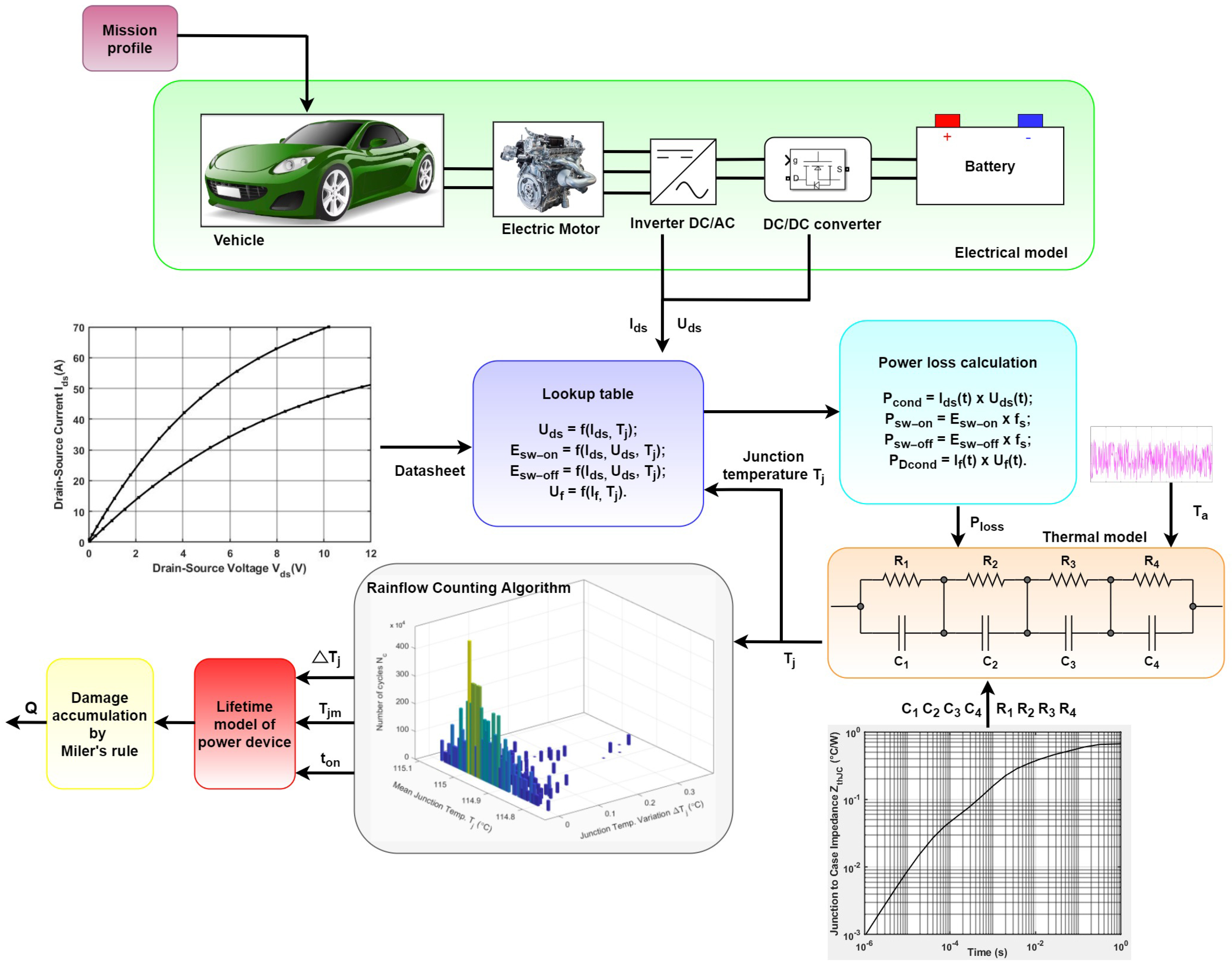
:1. Introduction
2. Electrical Model
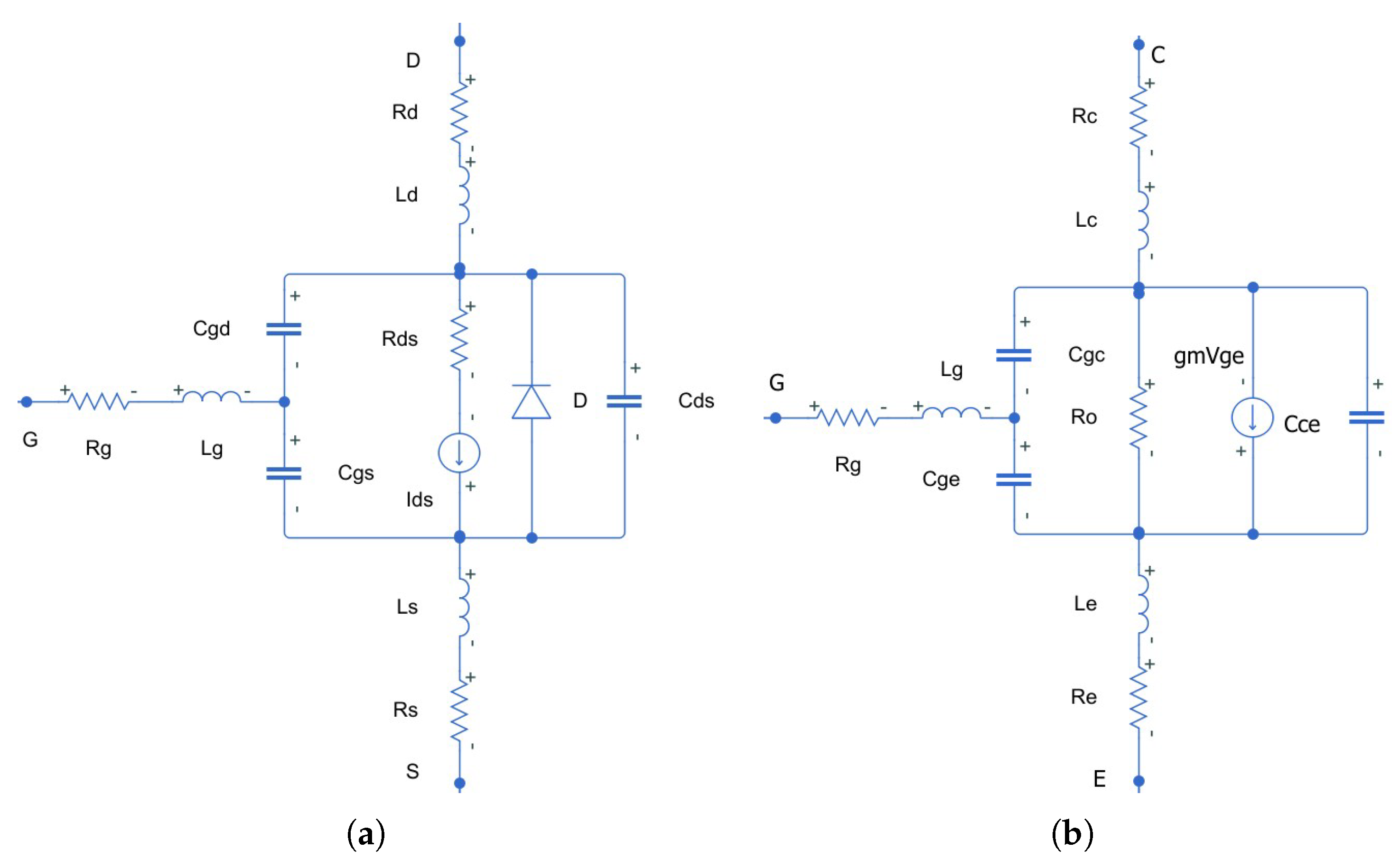
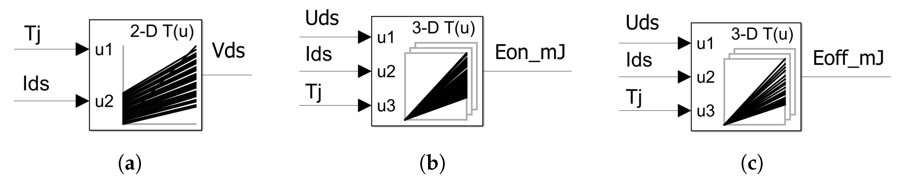
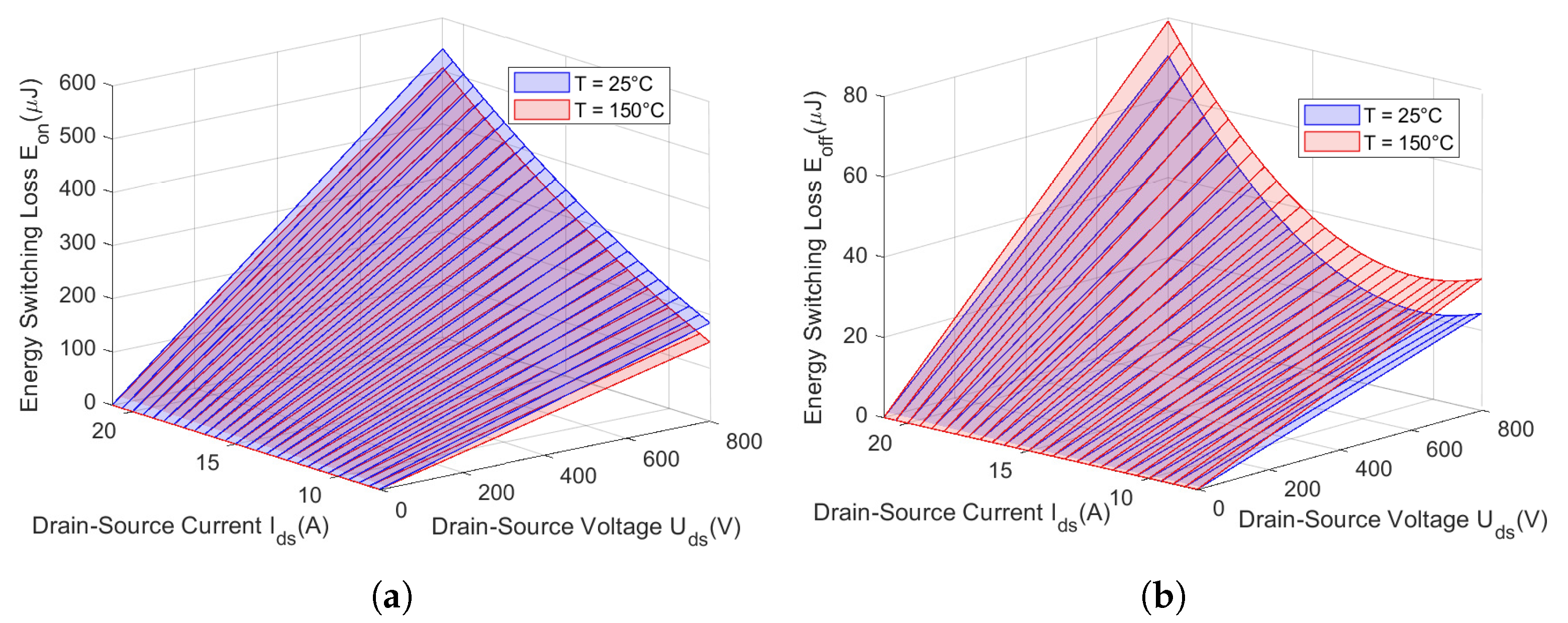
2.1. Mosfet Characteristic
2.2. IGBT Characteristic
2.3. Diode Characteristic
3. Power Losses Computation
3.1. Mosfet Power Losses
3.2. IGBT Power Loss
3.3. Diode Power Loss
4. Thermal Model
5. Temperature Measurement and Management
6. Lifetime Modeling
7. Mission Profiles
8. Rainflow Algorithms
9. Damage Accumulation
10. Conclusions
Author Contributions
Funding
Data Availability Statement
Conflicts of Interest
References
- Hu, Z.; Zhang, W.; Wu, J. An Improved Electro-Thermal Model to Estimate the Junction Temperature of IGBT Module. Electronics 2019, 8, 1066. [Google Scholar] [CrossRef]
- Rasool, H.; El Baghdadi, M.; Rauf, A.M.; Zhaksylyk, A.; D’hondt, T.; Sarrazin, M.; Hegazy, O. Accurate Electro-Thermal Computational Model Design and Validation for Inverters of Automotive Electric Drivetrain Applications. Appl. Sci. 2022, 12, 5593. [Google Scholar] [CrossRef]
- Xu, Y.; Ho, C.; Ghosh, A.; Muthumuni, D. A behavioral transient model of IGBT for switching cell power loss estimation in electromagnetic transient simulation. In Proceedings of the IEEE Applied Power Electronics Conference and Exposition (APEC) 2018, San Antonio, TX, USA, 4–8 March 2018; pp. 270–275. [Google Scholar]
- Nayak, D.P.; Pramanick, S.K. Implementation of an Electro-Thermal Model for Junction Temperature Estimation in a SiC MOSFET Based DC/DC Converter. CPSS Trans. Power Electron. Appl. 2023, 8, 42–53. [Google Scholar] [CrossRef]
- Morel, C.; Morel, J.-Y. Impact of Chaos on MOSFET Thermal Stress and Lifetime. Electronics 2024, 13, 1649. [Google Scholar] [CrossRef]
- Broeck, C.H.V.D.; Gospodinov, A.; Doncker, R.W.D. IGBT junction temperature estimation via gate voltage plateau sensing. IEEE Trans. Ind. Appl. 2018, 56, 4752–4763. [Google Scholar] [CrossRef]
- Cheng, T.; Lu, D.D.-C.; Siwakoti, P. A MOSFET SPICE Model With Integrated Electro-Thermal Averaged Modeling, Aging, and Lifetime Estimation. IEEE Access 2021, 9, 5545–5554. [Google Scholar] [CrossRef]
- Dusmez, S.; Akin, B. An accelerated thermal aging platform to monitor fault precursor on-state resistance. In Proceedings of the 2015 IEEE International Electric Machines & Drives Conference (IEMDC), Coeur d’Alene, ID, USA,, 10–13 May 2015; Volume 54, pp. 1352–1358. [Google Scholar]
- Baraniuk, R.; Todorenko, V.; Ushakov, D. Calculation of electrothermal processes in pulse converters to provide thermal protection. East. Eur. J. Enterp. Technol. 2016, 82, 19–25. [Google Scholar] [CrossRef]
- Shen, M.; Joseph, A.; Wang, J.; Peng, F.Z.; Adams, D.J. Comparison of traditional inverters and Z-source inverter for fuel cell vehicles. IEEE Trans. Power Electr. 2007, 22, 1453–1463. [Google Scholar] [CrossRef]
- Abdelhakim, A.; Davari, P.; Blaabjerg, F.; Mattavelli, P. Switching loss reduction in three-phase quasi-Z-source inverters utilizing modified space vector modulation strategies. IEEE Trans. Power Electr. 2017, 33, 4045–4060. [Google Scholar] [CrossRef]
- Iijima, R.; Isobe, T.; Tadano, H. Loss analysis of Z-source inverter using SiC-MOSFET from the perspective of current path in shoot-through mode. In Proceedings of the 2016 18th European Conference on Power Electronics and Applications (EPE’16 ECCE Europe), Karlsruhe, Germany, 5–9 September 2016; Volume 82, pp. 19–25. [Google Scholar]
- Bazzi, A.M.; Krein, P.T.; Kimball, J.W.; Kepley, K. IGBT and diode loss estimation under hysteresis switching. IEEE Trans. Power Electr. 2012, 27, 1044–1048. [Google Scholar] [CrossRef]
- Blaabjerg, F.; Pedersen, J.; Sigurjonsson, S.; Elkjaer, A. An extended model of power losses in hard-switched IGBT-inverters. IEEE Ind. Appl. Conf. 1996, 3, 1454–1463. [Google Scholar]
- Grgic, I.; Vukadinovic, D.; Basic, M.; Bubalo, M. Calculation of Semiconductor Power Losses of a Three-Phase Quasi-Z-Source Inverter. Electronics 2020, 9, 1642. [Google Scholar] [CrossRef]
- Franke, W.T.; Mohr, M.; Fuchs, F.W. Comparison of a Z-Source inverter and a voltage-source inverter linked with a DC/DC-boost-converter for wind turbines concerning their efficiency and installed semiconductor power. In Proceedings of the 2008 IEEE Power Electronics Specialists Conference, Rhodes, Greece, 15–19 June 2008. [Google Scholar]
- Lei, Q.; Peng, F.Z.; He, L.; Yang, S. Power loss analysis of current-fed quasi-Z-source inverter. In Proceedings of the IEEE Energy Conversion Congress and Exposition (ECCE 2010), Atlanta, GA, USA, 12–16 September 2010. [Google Scholar]
- Jahdi, S.; Alatise, O.; Ran, L.; Mawby, P. Accurate analytical modeling for switching energy of PiN diodes reverse recovery. IET Elect. Power Appl. 2015, 62, 1461–1470. [Google Scholar] [CrossRef]
- Gao, B.; Yanga, F.; Chen, M.; Chen, Y.; Laia, W.; Liuc, C. Thermal lifetime estimation method of IGBT module considering solder fatigue damage feedback loop. Microelectron. Reliab. 2018, 82, 51–61. [Google Scholar] [CrossRef]
- Li, Q.; Bai, H.; Breaz, E.; Roche, R.; Gao, F. Lookup Table-based Electro-Thermal Real-Time Simulation of Output Series Interleaved Boost Converter for Fuel Cell Applications. In Proceedings of the IECON 2021—47th Annual Conference of the IEEE Industrial Electronics Society, Toronto, ON, Canada, 13–16 October 2021; Volume 82, pp. 51–61. [Google Scholar]
- Ceccarelli, L.; Bahman, A.S.; Iannuzzo, F. Impact of device aging in the compact electro-thermal modeling of SiC power MOSFETs. Microelectron. Reliab. 2019, 100–101, 113336. [Google Scholar] [CrossRef]
- Liu, Y.; Tolbert, L.M.; Kritprajun, P.; Dong, J.; Zhu, L.; Ollis, T.B.; Schneider, K.P.; Prabakar, K. Fast Quasi-Static Time-Series Simulation for Accurate PV Inverter Semiconductor Fatigue Analysis with a Long-Term Solar Profile. Energies 2022, 15, 9104. [Google Scholar] [CrossRef]
- Choudhury, K.R.; Rogers, D.J. Steady-state thermal modeling of a power module: An n-layer fourier approach. IEEE Trans. Power Electron. 2018, 34, 1500–1508. [Google Scholar] [CrossRef]
- Janicki, M.; De Mey, G.; Napieralski, A. Application of Green’s functions for analysis of transient thermal states in electronic circuits. Microelectron. J. 2002, 33, 733–738. [Google Scholar] [CrossRef]
- Smail, T.; Dibi, Z.; Bendib, D. PSpice Implementation and Simulation of a New Electro-Thermal Modeling for Estimating the Junction Temperature of Low Voltage Power MOSFET. J. Nano Electron. Phys. 2018, 10, 06004. [Google Scholar] [CrossRef]
- Bahman, A.S.; Ma, K.; Ghimire, P.; Iannuzzo, F.; Blaabjerg, F. A 3-D-lumped thermal network model for long-term load profiles analysis in high-power IGBT modules. IEEE J. Emerg. Sel. Top. Power Electron. 2016, 3, 1050–1063. [Google Scholar] [CrossRef]
- Ziabari, A.; Park, J.H.; Ardestani, E.K.; Renau, J.; Kang, S.M.; Shakouri, A. Power blurring: Fast static and transient thermal analysis method for packaged integrated circuits and power devices. IEEE Trans. Very Large Scale Integr. Syst. 2014, 22, 2366–2379. [Google Scholar] [CrossRef]
- Nakamura, Y.; Evans, T.M.; Kuroda, N.; Sakairi, H.; Nakakohara, Y.; Otake, H.; Nakahara, H. Electrothermal Cosimulation for Predicting the Power Loss and Temperature of SiC MOSFET Dies Assembled in a Power Module. IEEE Trans. Power Electron. 2020, 35, 2950–2958. [Google Scholar] [CrossRef]
- Barbagallo, C.; Rizzo, S.A.; Scelba, G.; Scarcella, G.; Cacciato, M. On the Lifetime Estimation of SiC Power MOSFETs for Motor Drive Applications. Electronics 2021, 10, 324. [Google Scholar] [CrossRef]
- D’Alessandro, V.L.; CodecasaCatalano, A.P.; Scognamillo, C. Circuit based electrothermal simulation of multicellular SiC power MOSFETs using FANTASTIC. Energies 2020, 13, 4563. [Google Scholar] [CrossRef]
- Balachandran, R.; VijayaKumari, A. Thermal analysis for optimized selection of cooling techniques for SiC devices in high frequency switching applications. IOP Conf. Ser. Mater. Sci. Eng. 2019, 577, 012143. [Google Scholar] [CrossRef]
- Race, S.; Philipp, A.; Nagel, M.; Ziemann, T.; Kovacevic-Badstuebner, I.; Grossner, U. Circuit-Based Electrothermal Modeling of SiC Power Modules With Nonlinear Thermal Models. Proc. IEEE Trans. Power Electron. 2022, 37, 7965–7976. [Google Scholar] [CrossRef]
- Reichl, J.; Ortiz-Rodriguez, J.M.; Hefner, A.; Lai, J. 3-D thermal component model for electrothermal analysis of multichip power modules with experimental validation. IEEE Trans. Power Electron. 2015, 30, 3300–3308. [Google Scholar] [CrossRef]
- Shahjalal, M.; Shams, T.; Hossain, S.B.; Ahmed, M.R.; Ahsan, M.; Haider, J.; Goswami, R.; Alam, S.B.; Iqbal, A. Thermal analysis of Si-IGBT based power electronic modules in 50kW traction inverter application. E-Prime Adv. Electr. Eng. Electron. Energy 2023, 3, 100112. [Google Scholar] [CrossRef]
- Raciti, A.; Cristaldi, D.; Greco, D.; Vinci, G.; Bazzano, G. Electrothermal PSpice Modeling and Simulation of Power Modules. IEEE Trans. Ind. Electron. 2015, 62, 6260–6271. [Google Scholar] [CrossRef]
- Yang, X.; Xu, S.; Heng, K.; Wu, X. Distributed Thermal Modeling for Power Devices and Modules With Equivalent Heat Flow Path Extraction. IEEE J. Emerg. Sel. Top. Power Electron. 2023, 11, 5863–5876. [Google Scholar] [CrossRef]
- Ibrahim, A.; Khatir, Z.; Ousten, J.-P.; Lallemand, R.; Degrenne, N.; Mollov, S.; Ingrosso, D. Using of Bond-Wire Resistance as Ageing Indicator of Semiconductor Power Modules. Microelectron. Reliab. 2020, 114, 113757. [Google Scholar] [CrossRef]
- Held, M.; Jacob, P.; Nicoletti, G.; Scacco, P.; Poech, M.H. Fast power cycling test for IGBT modules in traction application. In Proceedings of the International Conference on Power Electronics and Drive Systems, Singapore, 26–29 May 1997; pp. 425–430. [Google Scholar] [CrossRef]
- Otto, A.; Rzepka, S. Lifetime modelling of discrete power electronic devices for automotive applications. In Proceedings of the AmE 2019—Automotive Meets Electronics; 10th GMM-Symposium, Dortmund, Germany, 12–13 March 2019; pp. 105–110. [Google Scholar]
- GopiReddy, L.R.; Tolbert, L.M.; Ozpineci, B. Power cycle testing of power switches: A literature survey. IEEE Trans. Power Electron. 2015, 30, 2465–2473. [Google Scholar]
- Dusmez, S.; Ali, S.H.; Heydarzadeh, M.; Kamath, A.S.; Duran, H.; Akin, B. Aging precursor identification and lifetime estimation for thermally aged discrete package silicon power switches. IEEE Trans. Ind. Appl. 2017, 53, 251–260. [Google Scholar] [CrossRef]
- Otto, A.; Rzepka, S.; Wunderle, B. Investigation of Active Power Cycling Combined with Passive Thermal Cycles on Discrete Power Electronic Devices. J. Electron. Packag. Trans. ASME 2019, 141, 031012. [Google Scholar] [CrossRef]
- Dupont, L.; Avenas, Y.; Jeannin, P.O. Comparison of Junction Temperature Evaluations in a Power IGBT Module Using an IR Camera and Three Thermosensitive Electrical Parameters. IEEE Trans. Ind. Appl. 2013, 49, 1599–1608. [Google Scholar] [CrossRef]
- Freire, S.D.; Deep, G.S. A p-n junction temperature sensor with switched current excitation. In Proceedings of the 1993 IEEE Instrumentation and Measurement Technology Conference, Irvine, CA, USA, 18–20 May 1993; Volume 49, pp. 310–315. [Google Scholar]
- Baker, N.; Munk-Nielsen, S.; Liserre, M.; Iannuzzo, F. Online junction temperature measurement via internal gate resistance during turn-on. In Proceedings of the 16th European Conference on Power Electronics and Applications (EPE’14—ECCE Europe), Lappeenranta, Finland, 26–28 August 2014; pp. 1–10. [Google Scholar]
- Stella, F.; Pellegrino, G.; Member, S.; Armando, E.; Dapr, D. Online junction temperature estimation of SiC power MOSFETS through onstate voltage mapping. IEEE Trans. Ind. Appl. 2018, 54, 3453–3462. [Google Scholar] [CrossRef]
- Baker, N.; Munk-Nielsen, S.; Iannuzzo, F.; Liserre, M. IGBT junction temperature measurement via peak gate current. IEEE Trans. Power Electron. 2016, 31, 3784–3793. [Google Scholar] [CrossRef]
- Barlini, D.; Ciappa, M.; Castellazzi, A.; Mermet-Guyennet, M.; Fichtner, W. New technique for the measurement of the static and of the transient junction temperature in IGBT devices under operating conditions. Microelectron. Reliab. 2006, 46, 1772–1777. [Google Scholar] [CrossRef]
- Bryant, A.; Yang, S.; Mawby, P.; Xiang, D.; Ran, L.; Tavner, P.; Palmer, P.R. Investigation into IGBT dv/dt during turn-off and its temperature dependence. IEEE Trans. Power Electron. 2011, 26, 3019–3031. [Google Scholar] [CrossRef]
- Luo, H.; Li, W.; Iannuzzo, F.; He, X.; Blaabjerg, F. Enabling junction temperature estimation via collector-side thermo-sensitive electrical parameters through emitter stray inductance in high-power igbt modules. IEEE Trans. Ind. Electron. 2018, 65, 4724–4738. [Google Scholar] [CrossRef]
- Yang, F.; Pu, S.; Xu, C.; Akin, B. Turn-on delay based real-time junction temperature measurement for SiC MOSFETs with aging compensation. IEEE Trans. Power Electron. 2021, 36, 1280–1294. [Google Scholar] [CrossRef]
- Zhang, Z.; Dyer, J.; Wu, X.; Wang, F.; Costinett, D.; Tolbert, L.M.; Blalock, B.J. Online junction temperature monitoring using intelligent gate drive for SiC power devices. IEEE Trans. Power Electron. 2019, 34, 7922–7932. [Google Scholar] [CrossRef]
- Chen, Z.; Gao, F.; Yang, C.; Peng, T.; Zhou, L.; Yang, C. Converter Lifetime Modeling Based on Online Rainflow Counting Algorithm. In Proceedings of the 2019 IEEE 28th International Symposium on Industrial Electronics (ISIE), Vancouver, BC, Canada, 12–14 June 2019; Volume 29, pp. 1743–1748. [Google Scholar]
- Andresen, M.; Ma, K.; Buticchi, G.; Falck, J.; Blaabjerg, F.; Liserre, M. Junction temperature control for more reliable power electronics. IEEE Trans. Power Electrononics 2017, 33, 765–776. [Google Scholar] [CrossRef]
- Wang, C.; Hua, L.; Yan, H.; Li, B.; Tu, Y.; Wang, R. A thermal management strategy for electronic devices based on moisture sorption-desorption processes. Joule 2020, 4, 435–447. [Google Scholar] [CrossRef]
- Emam, M.; Ookawara, S.; Ahmed, M. Thermal management of electronic devices and concentrator photovoltaic systems using phase change material heat sinks: Experimental investigations. Renew. Energy 2019, 141, 322–339. [Google Scholar] [CrossRef]
- Shamberger, P.J.; Bruno, N.M. Review of metallic phase change materials for high heat flux transient thermal management applications. Appl. Energy 2020, 258, 113955. [Google Scholar] [CrossRef]
- Li, W.; Wang, F.; Cheng, W.; Chen, X.; Zhao, Q. Study of using enhanced heat-transfer flexible phase change material film in thermal management of compact electronic device. Energy Convers. Manag. 2020, 210, 112680. [Google Scholar] [CrossRef]
- Talesara, V.; Garman, P.D.; Lee, J.L.; Lu, W. Thermal management of high-power switching transistors using thick cvd-grown graphene nanomaterial. IEEE Trans. Power Electron. 2020, 35, 578–590. [Google Scholar] [CrossRef]
- Wang, X.; Castellazzi, A.; Zanchetta, P. Regulated cooling for reduced thermal cycling of power devices. In Proceedings of the 7th International Power Electronics and Motion Control Conference, Harbin, China, 2–5 June 2012; pp. 238–244. [Google Scholar]
- Lin, X.; Mo, S.; Jia, L.; Yang, Z.; Chen, Y.; Cheng, Z. Experimental study and Taguchi analysis on LED cooling by thermoelectric cooler integrated with microchannel heat sink. Appl. Energy 2019, 242, 232–238. [Google Scholar] [CrossRef]
- Alhmoud, L. Reliability improvement for a high-power IGBT in wind energy applications. IEEE Trans. Ind. Elec. 2018, 65, 7129–7137. [Google Scholar] [CrossRef]
- Murdock, D.A.; Torres, J.E.R.; Connors, J.J.; Lorenz, R.D. Active thermal control of power electronic modules. IEEE Trans. Ind. Appl. 2006, 42, 552–558. [Google Scholar] [CrossRef]
- Wang, B.; Zhou, L.; Zhang, Y.; Wang, K.; Du, X.; Sun, P. Active junction temperature control of IGBT based on adjusting the turn-off trajectory. IEEE Trans. Power Electron. 2018, 33, 5811–5823. [Google Scholar] [CrossRef]
- Qin, Z.; Wang, H.; Blaabjerg, F.; Chiang, P. The Feasibility Study on Thermal Loading Control of Wind Power Converters with a Flexible Switching Frequency. IEEE Energy Convers. Congr. Expo. (ECCE). 2015, pp. 485–491. Available online: https://www.researchgate.net/publication/308807537_The_feasibility_study_on_thermal_loading_control_of_wind_power_converters_with_a_flexible_switching_frequency (accessed on 11 September 2023).
- Andresen, M.; Buticchi, G.; Liserre, M. Study of reliability-efficiency tradeoff of active thermal control for power electronic systems. Microelectron. Reliab. 2016, 58, 119–125. [Google Scholar] [CrossRef]
- Dong, Y.; Yang, H.; Li, W.; He, X. Neutral-point-shift-based active thermal control for a modular multilevel converter under a single-phase-to-ground fault. IEEE Trans. Ind. Elec. 2019, 66, 2474–2484. [Google Scholar] [CrossRef]
- Stella, F.; Pellegrino, G.; Armando, E. Three-phase SiC inverter with active limitation of all MOSFETs junction temperature. Microelectron. Reliab. 2020, 110, 113659. [Google Scholar] [CrossRef]
- Granados-Alejo, V.; Rubio-González, C.; Vázquez-Jiménez, C.A.; Banderas, J.A.; Gómez-Rosas, G.; Dibi, Z.; Bendib, D. Influence of specimen thickness on the fatigue behavior of notched steel plates subjected to laser shock peening. Opt. Laser Technol. 2018, 101, 531–544. [Google Scholar] [CrossRef]
- Chemisky, Y.; Hartl Darren, J.; Meraghni, F. Three-dimensional constitutive model for structural and functional fatigue of shape memory alloy actuators. Int. J. Fatigue 2018, 112, 263–278. [Google Scholar] [CrossRef]
- Kovačević, I.F.; Drofenik, U.; Kolar, J.W. New physical model for lifetime estimation of power modules. In Proceedings of the 2010 International Power Electronics Conference—ECCE ASIA, Sapporo, Japan, 9 August 2010. [Google Scholar]
- Rahimpour, S.; Tarzamni, H.; Kurdkandi, N.V.; Husev, O.; Tahami, F. An Overview of Lifetime Management of Power Electronic Converters. IEEE Access 2022, 10, 109688. [Google Scholar] [CrossRef]
- Scheuermann, U.; Schmidt, R. A new lifetime model for advanced power modules with sintered chips and optimized Al wire bonds. In Proceedings of the PCIM Europe, Nuremberg, Germany, 14–16 May 2013; pp. 810–817. [Google Scholar]
- Yang, L.; Agyakwa, P.A.; Johnson, C.M. Physics-of-failure lifetime prediction models for wire bond interconnects in power electronic modules. IEEE Trans. Device Mater. Rel. 2013, 13, 9–17. [Google Scholar] [CrossRef]
- Bielen, J.; Gommans, J.-J.; Theunis, F. Prediction of high cycle fatigue in aluminum bond wires: A physics of failure approach combining experiments and multi-physics simulation. In Proceedings of the EuroSime 2006—7th International Conference on Thermal, Mechanical and Multiphysics Simulation and Experiments in Micro-Electronics and Micro-Systems, Como, Italy, 24–26 April 2006; pp. 1–7. [Google Scholar]
- Kostandyan, E.E.; Sørensen, J.D. Physics of failure as a basis for solder elements reliability assessment in wind turbine. Rel. Eng. Syst. Saf. 2012, 108, 100–107. [Google Scholar] [CrossRef]
- Sarihan, V. Energy based methodology for damage and life prediction of solder joints under thermal cycling. IEEE Trans. Compon. Packag. Manuf. Technol. 1994, 17, 626–631. [Google Scholar] [CrossRef]
- Martin, H.A.; Smits, E.C.P.; Poelma, R.H.; van Driel, W.D.; Zhang, G.Q. Online Condition Monitoring Methodology for Power Electronics Package Reliability Assessment. IEEE Trans. Power Electron. 2024, 39, 4725–4734. [Google Scholar] [CrossRef]
- Yang, X.; Zhang, Y.; Wu, X.; Liu, G. Failure Mode Classification of IGBT Modules Under Power Cycling Tests Based on Data-Driven Machine Learning Framework. IEEE Trans. Power Electron. 2023, 38, 16130–16141. [Google Scholar] [CrossRef]
- Ziemann, T.; Neuenschwander, J. Power Cycling of Commercial SiC MOSFETs. In Proceedings of the IEEE 6th Workshop on Wide Bandgap Power Devices and Applications (WiPDA), Atlanta, GA, USA, 31 October–2 November 2018. [Google Scholar] [CrossRef]
- Zeng, G.; Borucki, L.; Wenzel, O.; Schilling, O.; Lutz, J. First results of development of a lifetime model for a transfer molded discrete power devices. In Proceedings of the PCIM Europe, Nuremberg, Germany, 5–7 June 2018; pp. 706–713. [Google Scholar]
- Silva, R.P.; de Barros, R.C.; Brito, E.M.S.; Boaventura, W.C.; Cupertino, A.F.; Pereira, H.A. Pursuing computationally efficient wear-out prediction of PV inverters: The role of the mission profile resolution. Microelectron. Reliab. 2020, 110, 113679. [Google Scholar] [CrossRef]
- Ferreira, V.N. Reliability-Oriented Strategies for Multichip Module Based Mission Critical Industry Applications. These 2021, 577, 012143. [Google Scholar]
- Sangwongwanich, A.; Zhou, D.; Liivik, E.; Blaabjerg, F. Mission profile resolution impacts on the thermal stress and reliability of power devices in PV inverters. Microelectron. Reliab. 2018, 88–90, 1003–1007. [Google Scholar] [CrossRef]
- Zhang, J.; Du, X.; Qian, C. Lifetime improvement for wind power generation system based on optimal effectiveness of thermal management. Appl. Energy 2021, 286, 116476. [Google Scholar] [CrossRef]
- Chen, Y.; Xie, F.; Zhang, H.; Qiu, D.; Chen, X.; Li, Z.; Zhang, G. Improvement of Stability in a PCM-Controlled Boost Converter with the Target Period Orbit-Tracking Method. Electronics 2019, 8, 1432. [Google Scholar] [CrossRef]
- Mainka, K.; Thoben, M.; Schilling, O. Counting Methods for Lifetime Calculation of Power Modules. In Proceedings of the 2011—14th European Conference on Power Electronics and Applications (EPE), Birmingham, UK, 30 August–1 September 2011; pp. 35–39. [Google Scholar]
- Mainka, K.; Thoben, M.; Schilling, O. Lifetime calculation for power modules application and theory of models and counting methods. In Proceedings of the 2011—14th European Conference on Power Electronics and Applications (EPE), Birmingham, UK, 30 August–1 September 2011; pp. 1–8. [Google Scholar]
- Ali, S.H.; Heydarzadeh, M.; Dusmez, S.; Li, X.; Kamath, A.S.; Akin, B. Lifetime Estimation of Discrete IGBT Devices Based on Gaussian Process. IEEE Trans. Ind. Appl. 2018, 54, 395–403. [Google Scholar] [CrossRef]
- Sonsino, C.M. Fatigue testing under variable amplitude loading. Int. J. Fatigue 2007, 29, 1080–1089. [Google Scholar] [CrossRef]
- Azamfar, M.; Moshrefifar, M. Moshrefifar and Azamfar method, a new cycle counting method for evaluating fatigue life. Int. J. Fatigue 2014, 69, 2–15. [Google Scholar] [CrossRef]
- Downing, S.D.; Socie, D.F. Simple rainflow counting algorithms. Int. J. Fatigue 1982, 4, 31–40. [Google Scholar] [CrossRef]
- E1049–85; Standard Practice for Cycle Counting in Fatigue Practices. ASTM: West Conshohocken, PA, USA, 2011.
- McInnes, C.H.; Meehan, P.A. Equivalence of four-point and three-point rainflow cycle counting algorithms. Int. J. Fatigue 2008, 30, 547–559. [Google Scholar] [CrossRef]
- Antonopoulos, A.; D’Arco, S.; Hernes, M.; Peftitsis, D. Challenges and strategies for a real-time implementation of a Rainflow-counting algorithm for fatigue assessment of power modules. In Proceedings of the 2019 IEEE Applied Power Electronics Conference and Exposition (APEC), Anaheim, CA, USA, 17–21 March 2019; Volume 29, pp. 2708–2713. [Google Scholar]
- Cluff, K.D.; Robbins, D.; Edwards, T.; Barker, B. Characterizing the commercial avionics thermal environment for field reliability assessment. J. Inst. Environ. Sci. 1997, 40, 22–28. [Google Scholar] [CrossRef]
- Denk, M.; Bakran, M. Comparison of counting algorithms and empirical lifetime models to analyze the load-profiles of IGBT power module in a hybrid car. In Proceedings of the 2013 3rd International Electric Drives Production Conference (EDPC), Nuremberg, Germany, 29–30 October 2013; pp. 1–6. [Google Scholar]
- Twomey, J.M.; Chen, D.Y.; Osterman, M.D.; Pecht, M.G. Development of a cycle counting algorithm with temporal parameters. Microelectron. Reliab. 2020, 109, 113652. [Google Scholar] [CrossRef]
- Vichare, N. Prognostics and Health Management of Electronics by Utilizing Environmental and Usage Loads. Ph.D. Thesis, Department of Mechanical Engineering, University of Maryland, College Park, MD, USA, 2006. [Google Scholar]
- Cheng, T.; Lu, D.D.-C.; Siwakoti, Y.P. Circuit-Based Rainflow Counting Algorithm in Application of Power Device Lifetime Estimation. Energies 2022, 15, 5159. [Google Scholar] [CrossRef]
- Matlab. Rainflow Counts for Fatigue Analysis. Available online: https://au.mathworks.com/help/signal/ref/rainflow.html (accessed on 14 June 2022).
- Kardan, F.; Shekhar, A.; Bauer, P. Quantitative Comparison of the Empirical Lifetime Models for Power Electronic Devices in EV Fast Charging Application. In Proceedings of the 11th International Conference on Power Electronics—ECCE Asia, Jeju, Korea, 22–25 May 2023; pp. 3239–3244. [Google Scholar]
- Gatla, R.K.; Chen, W.; Zhu, G.; Zeng, D.; Nirudi, R. Lifetime estimation of modular cascaded H-bridge MLPVI for grid-connected PV systems considering mission profile. Microelectron. Reliab. 2018, 88–90, 1051–1056. [Google Scholar] [CrossRef]
- Ikonen, M. Power Cycling Lifetime Estimation of IGBT Power Modules Based on Chip Temperature Modeling. Ph.D. Thesis, Lappeenranta University of Technology, Lappeenranta, Finland, 11 December 2012. [Google Scholar]
- El-rafii, H.; Galadi, A. Improved Temperature-Scalable DC model for SiC power MOSFET including Quasi-Saturation effect. Solid-State Electron. 2024, 220, 108993. [Google Scholar] [CrossRef]
- Yang, J.; Wei, S.; Xu, D.; Liu, X. A variable-temperature parameter model for SiC MOSFETs considering parasitic parameters. Int. J. Front. Eng. Technol. 2024, 6, 6–12. [Google Scholar]
- Yang, J. Accurate Characterisation and Modelling of SiC MOSFETs for Transient Simulation. Ph.D. Thesis, Cardiff University, Cardiff, UK, 2022. [Google Scholar]
- Mohamed, B.; Elmostafa, E.; Imane, A.A. A Behavior Electrical Model of the MOSFET Using Matlab/Simulink. In Proceedings of the 2022 4th Global Power, Energy and Communication Conference (GPECOM), Nevsehir, Turkey, 14–17 June 2022. [Google Scholar]
- Stark, R.; Tsibizov, A.; Nain, N.; Grossner, U.; Kovacevic-Badstuebner, I. Accuracy of Three Interterminal Capacitance Models for SiC Power MOSFETs Under Fast Switching. IEEE Tran. Power Electron. 2021, 36, 9398–9410. [Google Scholar] [CrossRef]
- Nguyen, Q.C.; Tounsi, P.; Fradin, J.-P.; Reynes, J.-M. Development of SiC MOSFET Electrical Model and Experimental Validation: Improvement and Reduction of Parameter Number. In Proceedings of the 2019 MIXDES—26th International Conference—Mixed Design of Integrated Circuits and Systems, Rzeszow, Poland, 27–29 June 2019. [Google Scholar]
- Guan, L.; Zeng, P.; Zhang, X.; Li, Q.; Chen, Y.; Zhai, J.; Zhang, F.; Yang, B.; Cui, X.; Ye, J.; et al. The collector current model of the IGBT based on the gate charge. Microelectron. Reliab. 2024, 159, 115432. [Google Scholar] [CrossRef]
- Wolfspeed. C2M0080120D Silicon Carbide Power MOSFET C2M MOSFET Technology. Product Datasheet; Wolfspeed, 2023, Rev. 5, 11. Available online: https://assets.wolfspeed.com/uploads/2024/01/Wolfspeed_C2M0080120D_data_sheet.pdf (accessed on 11 September 2023).
- Górecki, P. A new electrothermal average model of the diode–transistor switch. Microelectron. Reliab. 2008, 48, 51–58. [Google Scholar] [CrossRef]
- Brincker, M.; Pedersen, K.B.; Kristensen, P.K.; Popok, V.N. Effects of thermal cycling on aluminum metallization of power diodes. Microelectron. Reliab. 2015, 55, 1988–1991. [Google Scholar] [CrossRef]
- Race, S.; Ziemann, T.; Tiwari, S.; Kovacevic-Badstuebner, I.; Grossner, U. Accuracy of thermal analysis for SiC power devices. Proc. IEEE Int. Rel. Phys. Symp 2021, 1–5. [Google Scholar] [CrossRef]
- Montaine, M.; Hanke, M.; Scheuermann, U. Direct 2-way coupled electro-thermal simulation of temperature and current distribution in power devices. In Proceedings of the PCIM Europe 2018; International Exhibition and Conference for Power Electronics, Intelligent Motion, Renewable Energy and Energy Management, Nuremberg, Germany, 5–7 June 2018; pp. 1–8. [Google Scholar]
- Codecasa, L.; d’Alessandro, V.; Magnani, A.; Irace, A. Circuit-based electrothermal simulation of power devices by an ultrafast nonlinear MOR approach. IEEE Trans. Power Electron. 2016, 31, 5906–5916. [Google Scholar] [CrossRef]
- Hyunseok, O.; Bongtae, H.; McCluskey, P.; Changwoon, H.; Youn, B.D. Physics-of-failure, condition monitoring, and prognostics of insulated gate bipolar transistor modules: A review. IEEE Trans. Power Electron. 2015, 30, 2413–2426. [Google Scholar]
- Rasool, H.; Verbrugge, B.; Zhaksylyk, A.; Tran, T.M.; El Baghdadi, M.; Geury, T.; Hegazy, O. Design Optimization and Electro-Thermal Modeling of an Off-Board Charging System for Electric Bus Applications. IEEE Access 2021, 8, 84501–84519. [Google Scholar] [CrossRef]
- Corten, H.; Dolan, T. Cumulative Fatigue Damage. In Proceedings of the International Conference on Fatigue of Metals, New York, NY, USA, 28–30 September 1956; pp. 235–242. [Google Scholar]
- Zhu, S.-P.; Huang, H.-Z.; Liu, Y.; He, L.-P.; Liao, Q. A Practical Method for Determining the Corten-Dolan Exponent and Its Application to Fatigue Life Prediction. Int. J. Turbo Jet-Engines 2012, 29, 79–87. [Google Scholar] [CrossRef]
- Hamasha, S.; Jaradat, Y.; Qasaimeh, A.; Obaidat, M.; Borgesen, P. Assessment of Solder Joint Fatigue Life Under Realistic Service Conditions. J. Electron. Mater. 2014, 43, 4472–4486. [Google Scholar] [CrossRef]
- Su, S.; Akkara, F.J.; Thaper, R.; Alkhazali, A.; Hamasha, M.; Hamasha, S. A State-of-the-Art Review of Fatigue Life Prediction Models for Solder Joint. J. Electron. Packag. 2019, 141, 040802. [Google Scholar] [CrossRef]
- Chen, Y.; Men, W.; Yuan, Z.; Kang, R.; Mosleh, A. Nonlinear Damage Accumulation Rule for Solder Life Prediction Under Combined Temperature Profile With Varying Amplitude. IEEE Trans. Components Packag. Manuf. Technol. 2018, 9, 39–50. [Google Scholar] [CrossRef]
- Amirpour, S.; Thiringer, T.; Hagstedt, D. Mission-Profile-Based Lifetime Study for SiC/IGBT Modules in a Propulsion Inverter. In Proceedings of the IEEE 19th International Power Electronics and Motion Control Conference (PEMC), Gliwice, Poland, 25–29 April 2021. [Google Scholar]
- Spejo, L.B.; Akor, I.; Rahimo, M.; Minamisawa, R.A. Life-cycle energy demand comparison of medium voltage Silicon IGBT and Silicon Carbide MOSFET power semiconductor modules in railway traction applications. Power Electron. Devices Components 2023, 6, 100050. [Google Scholar] [CrossRef]
- Dbeiss, M. Vieillissement Accéléré de Modules de Puissance de Type MOSFET SiC et IGBT Si Basé sur l’Analyse de Profils de Mission d’Onduleurs Photovoltaïques. 2018, pp. 1–201. Available online: https://theses.hal.science/tel-01869018 (accessed on 11 September 2023).


| Application | Mission Profile 1 | Mission Profile 2 |
|---|---|---|
| (a) Automotive application: inverter’s frequency mission profile. |  | |
| (b) Electrical motor: the new European driving cycle speed and city profiles. |  | 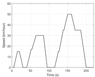 |
| (c) Wound Rotor Synchronous Machine: speed and torque profiles. |  |  |
| (d) Photovoltaic application: solar irradiance mission profiles with two minutes resolution during clear and cloudy days. |  | 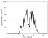 |
| (e) Wind power system: wind speed and ambiant temperature profiles. |  | 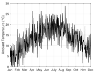 |
| (f) Power boost converter: periodic and chaotic Mosfet current profiles with a constant load. |  |  |
Disclaimer/Publisher’s Note: The statements, opinions and data contained in all publications are solely those of the individual author(s) and contributor(s) and not of MDPI and/or the editor(s). MDPI and/or the editor(s) disclaim responsibility for any injury to people or property resulting from any ideas, methods, instructions or products referred to in the content. |
© 2024 by the authors. Licensee MDPI, Basel, Switzerland. This article is an open access article distributed under the terms and conditions of the Creative Commons Attribution (CC BY) license (https://creativecommons.org/licenses/by/4.0/).
Share and Cite
Morel, C.; Morel, J.-Y. Power Semiconductor Junction Temperature and Lifetime Estimations: A Review. Energies 2024, 17, 4589. https://doi.org/10.3390/en17184589
Morel C, Morel J-Y. Power Semiconductor Junction Temperature and Lifetime Estimations: A Review. Energies. 2024; 17(18):4589. https://doi.org/10.3390/en17184589
Chicago/Turabian StyleMorel, Cristina, and Jean-Yves Morel. 2024. "Power Semiconductor Junction Temperature and Lifetime Estimations: A Review" Energies 17, no. 18: 4589. https://doi.org/10.3390/en17184589
APA StyleMorel, C., & Morel, J.-Y. (2024). Power Semiconductor Junction Temperature and Lifetime Estimations: A Review. Energies, 17(18), 4589. https://doi.org/10.3390/en17184589