Abstract
To enhance the power density of LLC resonant converters, multilayer planar inductors are required. However, multilayer planar inductors have high parasitic capacitance, which may cause inductor current ringing in LLC resonant converters, leading to EMI problems. In this paper, it is found that by using interleaved winding inductors, compared with traditional winding inductors, the parasitic capacitance of multilayer planar inductors is reduced, which can reduce current ringing, without sacrificing power density and increasing manufacturing complexity. The method used to analyze current ringing is to establish an impedance model, and the parasitic capacitance of the interleaved winding inductors is verified by FEM simulations. The analysis is validated in an LLC resonant converter prototype.
1. Introduction
High power density converters are key devices for achieving efficient energy conversion and management, and are widely used in renewable energy, smart grids, electric vehicles, and other applications. To enhance the high power density of converters, planar transformers and inductors with printed circuit board windings are used, which reduce the converter volume and facilitate production and assembly. However, the design of planar magnetic components needs to be optimized, as the inevitable parasitic capacitance of planar magnetic components alters the impedance characteristics of the circuit and causes common-mode noise and current ringing in the converter, which affects its performance and electromagnetic compatibility. Common-mode noise and current ringing can be reduced by using an optimized design for planar transformers, as verified by experiments.
In the application of resonant converters, the common-mode noise caused by the parasitic capacitance between the primary windings of the planar transformer is described in [1], where a verification experiment was conducted with an LLC resonant converter. Regarding the influence of the parasitic capacitance of the planar transformer on impedance, Refs. [2,3,4,5] conducted an impedance analysis, calculated the influence of the low-impedance transmission path of the common-mode noise, and described the current expression of the common-mode noise. To address this issue, Ref. [6] proposed the Y-capacitor method, which controls the common-mode noise conduction path and reduces EMI noise effectively, but this method cannot be applied to resonant converters. Therefore, Ref. [7] proposed a design scheme to eliminate common-mode noise in LLC resonant converters by using common-mode inductors. The implementation method is to design the resonant inductor as two series common-mode inductors, thereby eliminating common-mode noise. However, the resonant inductor needs to occupy more PCB area, which is not conducive to improving the converter power density.
For the analysis of the parasitic capacitance of the inductor, Refs. [8,9,10] give an accurate calculation model of inductor parasitic capacitance and verify it in a DAB active full-bridge converter. In [11], the causes of planar inductor parasitic capacitance were analyzed; a planar inductor structure optimization scheme was designed; and the parasitic capacitance was reduced. Moreover, Ref. [12] defined the resonance frequency caused by the parasitic capacitance of the inductor as the first resonance frequency, and gave an accurate calculation. Furthermore, Ref. [13] analyzed the parasitic capacitance in series and parallel windings, and used the method of combining the series and parallel windings to reduce the parasitic capacitance of the inductor. Methods for reducing the parasitic parameters of planar magnetic components were summarized in [14], and it was verified that the parasitic capacitance can be effectively reduced by optimizing the winding design. Reducing current ringing can decrease the EMI issues of converters, as demonstrated in [15,16,17,18]; thus, mitigating current ringing is an important technique to reduce the EMI problems in converters.
In this paper, an optimized design of a resonant inductor for a high-power density converter based on LLC resonant topology is proposed, which reduces the current ringing of the converter. Therefore, the structure of this paper is as follows: Section 2 analyzes the impedance model of the LLC resonant converter with parasitic capacitance of the resonant inductor and obtains the method of calculating the ringing current. Section 3 analyzes the parasitic capacitance of the resonant inductor suitable for high power density converters. Section 4 presents the comparative experimental results, and Section 5 concludes this paper.
2. Analysis of Impedance and Current Ringing
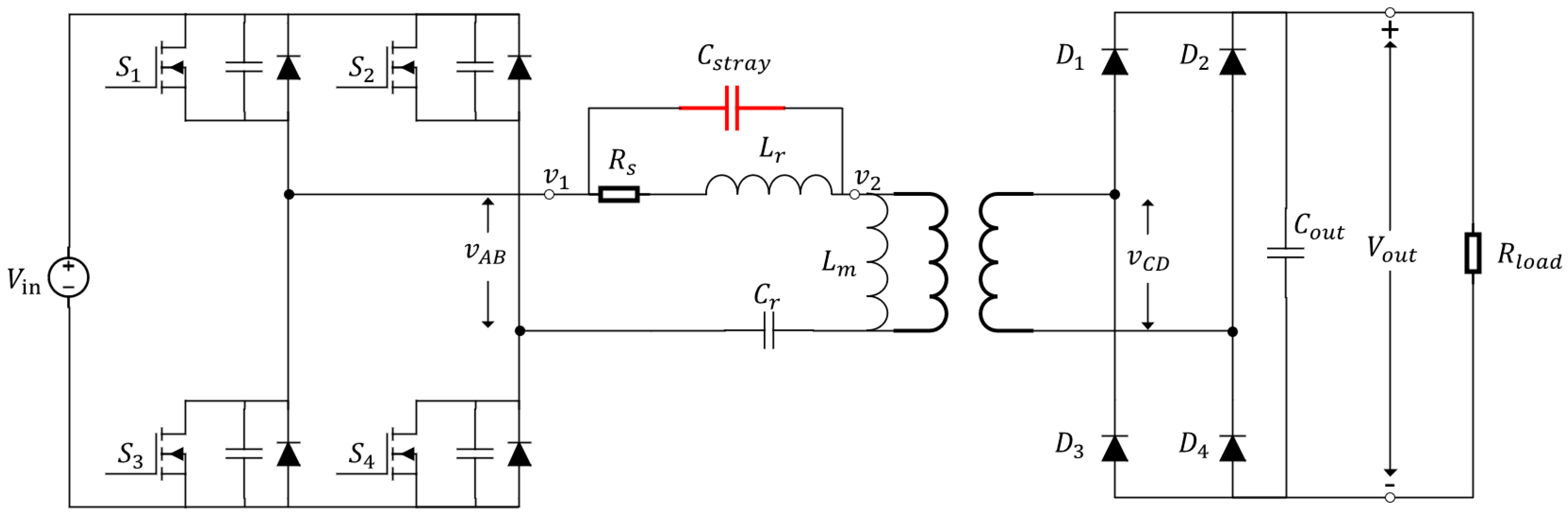
As shown in Figure 1, the LLC resonant converter consists of a full bridge, a rectifier bridge, and resonant components. The full bridge contains four power switches , , , and , and the rectifier bridge consists of four rectifier diodes , , , and . The resonant components form the resonant tank, including the influence of the parasitic capacitance of the resonant inductance ; in this paper, the modeling of the LLC resonant converter adds the parasitic capacitance of the resonant inductance. Figure 1 shows the equivalent circuit model of the LLC resonant converter with the parasitic capacitance of the resonant inductance. In this model, and are the two voltages generated by the full bridges on the input and output sides, respectively, and and are the node voltages.
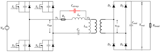
Figure 1.
The LLC converter considering parasitic capacitance of resonant inductor.
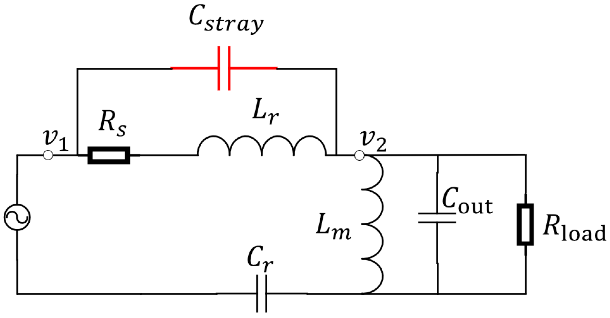
According to previous research, the parasitic parameters have an impact on the input impedance and output impedance of the converter, and the equivalent model of the resonant inductor is shown in Figure 2. As known from previous research, the parasitic capacitance creates a low-impedance path for the high-frequency voltage content, and the higher harmonics caused by the in the circuit are the source of the ringing current. This will generate high-frequency current ringing on the primary side, resulting in oscillating energy, which causes losses and electromagnetic compatibility problems, both of which are undesirable effects. In this scenario, the voltage and impedance models should be considered. Therefore, to analyze the ringing current of the LLC resonant converter, it is necessary to establish the time domain equation of the ringing current, shown in (1).
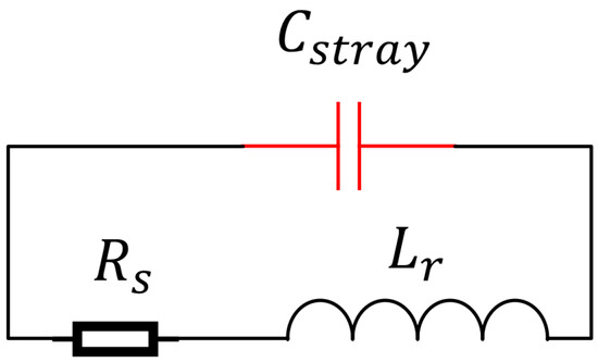
Figure 2.
Equivalent model of resonant inductor with parasitic capacitance.
As shown by the equivalent impedance diagram in Figure 3, is the node voltage value of the voltage of the parasitic capacitance of the input resonant inductor and is the node voltage value of the voltage of the parasitic capacitance of the output resonant inductor. According to the impedance relationship, it can be known that is numerically equal to the input voltage and is equal to the voltage of the resonant capacitor . The voltage of the resonant capacitor can be obtained from the input voltage by the impedance relationship. In order to obtain , the input impedance and partial impedance are defined, respectively, and the expressions are shown in (2).
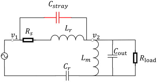
Figure 3.
Equivalent input impedance model of the LLC converter.
The input impedance is defined as the total impedance from the input voltage to the load, and the partial impedance is defined as the impedance excluding the resonant inductor and its parasitic capacitance. with and , the expression of can be obtained from the input voltage , as shown in (3), where is the equal impedance of the resonant inductor and its parasitic capacitance, as shown in (4).
Substituting (2)–(4) into (1), the expression of current ringing represented by the parasitic capacitance , the input voltage , and the impedances and can be obtained, as shown in (5), where , which is called the ringing impedance, is shown in (6).
By the harmonic component analysis method, it can be known that the high-frequency harmonics contained in can be expressed as (7), and, after rearrangement, as shown in (8).
It can be seen from (8) that the amplitude of the higher harmonics decreases with the increase in harmonic order. By substituting (8) into (5), the expression of current ringing can be further obtained, as shown in (9).
As shown in (9), we can see that the current ringing can reduce with the decrease in parasitic capacitance. In this study, the resonant inductance value of the LLC resonant converter is set to 2 μH, where the resonant capacitance and the resonant inductance are 40 nH and 10 μH, respectively. The bode diagrams of and are calculated using Matlab (R2022a) with the parasitic capacitance of the resonant inductance set to 565 pF, as shown in Figure 4a–c.
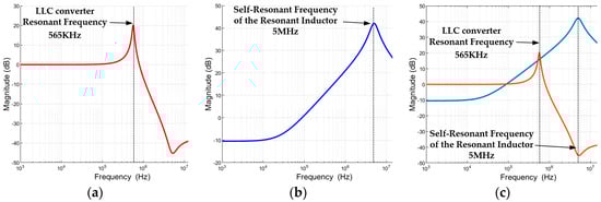
Figure 4.
Bode diagrams of impedance: (a) Bode diagrams of ; (b) Bode diagrams of ; (c) Comparison of bode diagrams: red for , blue for .
In Figure 4a, the red curve represents the Bode diagram curve of and the blue curve shown in Figure 4b depicts the Bode diagram curve of . From the Bode diagram, it is shown that the resonance point of is 565 kHz, which coincides with the resonant frequency of the LLC resonant converter. From the bode diagram curves of and , it can be observed that the harmonic impedance attains the minimum at 5 MHz, which leads to a low-impedance path in the LLC resonant converter, corresponding to the self-resonant frequency of the resonant inductor with parasitic capacitance. As demonstrated by the calculation results, the expression (9) can be further verified, indicating that the parasitic capacitance of the resonant inductor decreases; thus, the current ringing can be reduced.
3. Stray Capacitance of Multilayer Planar Inductor
As discussed in the previous section, the parasitic capacitance of the resonant inductor causes current ringing for the LLC resonant converter. Therefore, when the planar inductor is used as the resonant inductor of the LLC resonant converter, the parasitic capacitance of the planar inductor should be reduced by optimizing the structural design of the planar inductor winding. To satisfy the design requirements of high power density converters, the resonant inductors should also be designed with high power density. Hence, the area of the printed circuit boards for the windings of the planar inductors should be minimized. The planar inductors consist of printed circuit board windings with a wide width to enhance their current carrying and heat dissipation capabilities. To meet the inductance design parameters, the required inductance value parameters are achieved by using multilayer windings in series. Moreover, the planar inductors employ parallel-connected multiple windings to further increase their current carrying capability.
3.1. Design of Planar Inductors and Calculation of Parasitic Capacitance
In this study, we designed planar inductors with 2 µH inductance using the E22 ferrite core and the 3F4 core material from Ferroxcube. This prevented inductor saturation and allowed for the planar inductors to operate at frequencies above 1 MHz. We applied the inductor turns number design formula, as shown in (10).
where is the inductance value of the designed inductor, is the magnetic path length of the E22 core, and is the cross-sectional area of the E22 core. Using Equation (10) to calculate the required turns number of an inductor, the turns of the winding should be four turns. We designed a two-layer printed circuit board in series with a four-turn winding structure, with two turns in a single layer and a turn width of 2.5 mm in every turn. The outer turn of the winding in a single-layer printed circuit board had a length of 89.564 mm and the inner turn had a length of 54.173 mm, Figure 5b shows a cross-sectional diagram of the traditional winding design of a planar inductor.
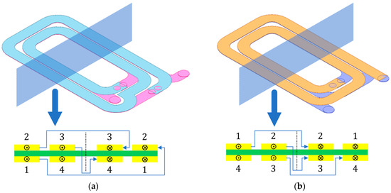
Figure 5.
Schematic diagram of planar inductor winding methods: (a) interleaved winding method; (b) traditional winding method.
According to the definition of parasitic capacitance of multilayer conductors, the parasitic capacitance value of the planar inductor depends on the interlayer energy and the input voltage. The calculation formula is shown in Equation (11).
is the parasitic capacitance obtained by using the energy relation, also known as dynamic capacitance; is the total energy, which is the sum of the energy between adjacent copper layers. is the voltage value on the multilayer planar inductor.
The energy calculation method between adjacent copper layers is shown in Equation (12), where is the voltage difference between the upper and lower adjacent copper layers; is the electrostatic capacitance between the conductors, which is only determined by the dielectric constant, the overlapping area of the conductors, and the distance between the adjacent conductors; is the relative permittivity of the medium between the conductors; is the relative permittivity in vacuum; is the overlapping area of the upper and lower adjacent copper layers; and is the distance between the upper and lower adjacent copper layers.
As shown in (12), optimizing the parasitic capacitance without changing the line width reduces the voltage difference between the adjacent copper layers. Since in a traditional winding method, the voltage drops to half of the voltage on the planar inductor when a single-layer two-turn winding is finished, there is a large potential difference between the upper and lower adjacent copper layers in a traditional winding method. Considering that the voltage drop in the winding is uniform, a two-turn winding that is traditionally wound on the same layer should be changed to a two-turn winding that is wound up and down; this design is an interleaved winding design, and a cross-sectional diagram of the interleaved winding design is shown in Figure 5a. Similarly, in a single-layer PCB, the width of the winding is 2.5 mm and the line width of each turn is equal, a length of the outer turn of the winding is 89.564 mm, and a length of the inner turn is 54.173 mm.
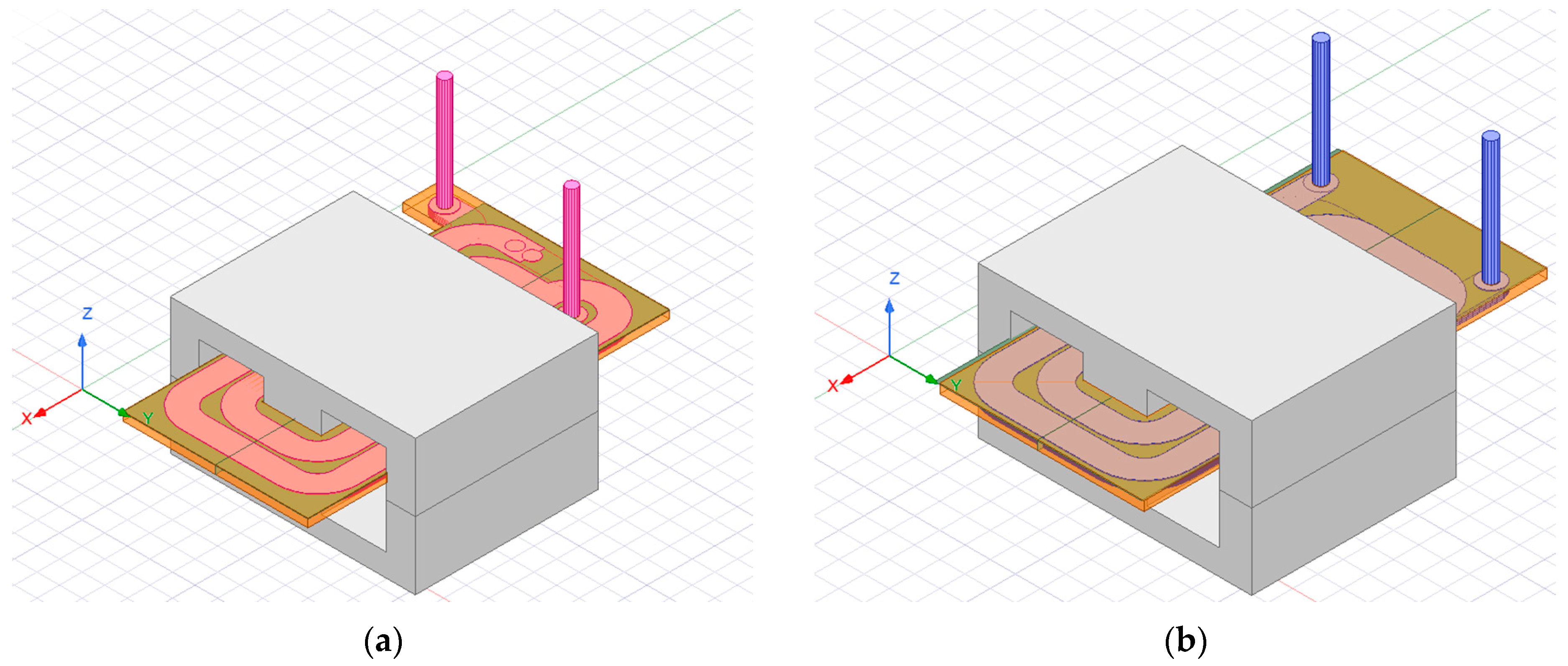
In order to reduce the cost of the verification experiment and verify the parasitic capacitance of the planar inductor with multilayer winding, a flexible printed circuit board was used to design the verification of the planar inductor with multilayer winding. The single-layer winding consisted of two turns, and six windings were connected in parallel to form a 12-layer PCB structure, which constituted a multilayer planar inductor winding. The single FPC used has two copper layers, with a thickness of 0.11 mm and a copper layer thickness of 1/3OZ. The distance between adjacent copper layers is 50 µm. Six flexible printed circuit boards are stacked and connected in parallel, as in the 3D model shown in Figure 6.

Figure 6.
Three-dimensional model of planar inductor: (a) interleaved winding inductor; (b) traditional winding inductor.
Therefore, according to Equation (12), the electrostatic capacitance values of the outer turns of the two planar inductor winding structures are both 63 pF, and the electrostatic capacitance value of the inner turn is 39 pF. The different parasitic capacitance values of the two winding structures are due to the potential difference between the upper and lower adjacent conductor layers. Assuming that the voltage on the planar inductor is 12 V, the parasitic capacitance values of the traditional and interleaved winding designs are calculated by Equation (11). The parasitic capacitance of the resonant inductor with traditional winding is 257 pF, and the parasitic capacitance of the resonant inductor with interleaved winding is 117 pF.
3.2. Finite Element Analysis and Simulation Verification of Planar Inductor Parasitic Capacitance
To verify the theoretical analysis, FEM analysis is presented to verify the parasitic capacitance of multilayer planar inductors. ANSYS Maxwell 2021 R1 is used to simulate the electric field distribution and extract the total equivalent capacitance. To reduce computational complexity, the 3D simulation results of the inductor can be easily calculated for each turn. The 3D simulation model was constructed based on the winding structure shown in Figure 6, with both inductor designs having the same thickness and width of the copper foil, number of layers per winding, distance between layers, length of the outer and inner turns of the winding, number of flexible PCB layers used per winding, and the number of windings in parallel. Specifically, the thickness of the copper foil was 1/3OZ, the width was 2.5 mm, the number of turns per winding was 4, the number of windings in parallel was 6, the number of flexible PCB layers used per winding was 2, the distance between layers was 50 µm, the length of the outer turn of the winding was 89.564 mm, and the length of the inner turn was 54.173 mm. During simulation, the same voltage excitation was applied to both winding models, with a value of 12 V and a frequency of 450 kHz.
Since the specifications of the windings were identical, with the exception of the winding method, and the voltage excitation frequency used in the simulation was consistent, the dc impedance of both winding designs was 29 mΩ. As for the AC impedance, it is primarily influenced by the skin effect and proximity effect. References [19,20] have calculated the AC impedance caused by the skin and proximity effects on copper foil, with the calculation method shown in Equation (13).
In Equation (13), and represent the impedance contributions from the skin effect and proximity effect, respectively. The coefficient denotes the relationship between the spacing and the thickness of adjacent copper layers, is the skin depth, is the frequency, is the permeability of free space, and is the electrical conductivity of copper, with being the number of adjacent copper layers. Given that the winding designs for both inductors were such that the inner and outer turns of the same copper layer have identical lengths, and the spacing between adjacent copper layers was the same, calculations using Equation (13) reveal that the AC impedance due to the proximity effect for both winding structures was 30.16 mΩ, the AC impedance due to the proximity effect was 1.48 Ω, and the total AC impedance for both designs was 1.52 Ω.
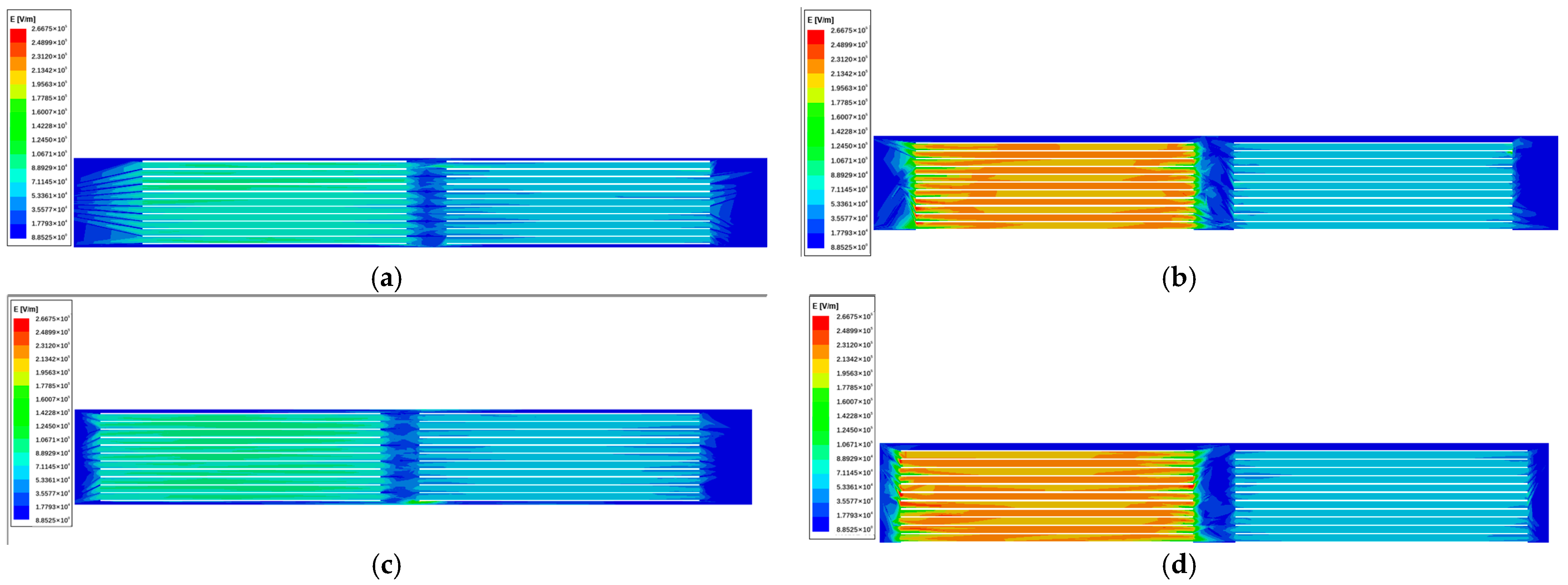
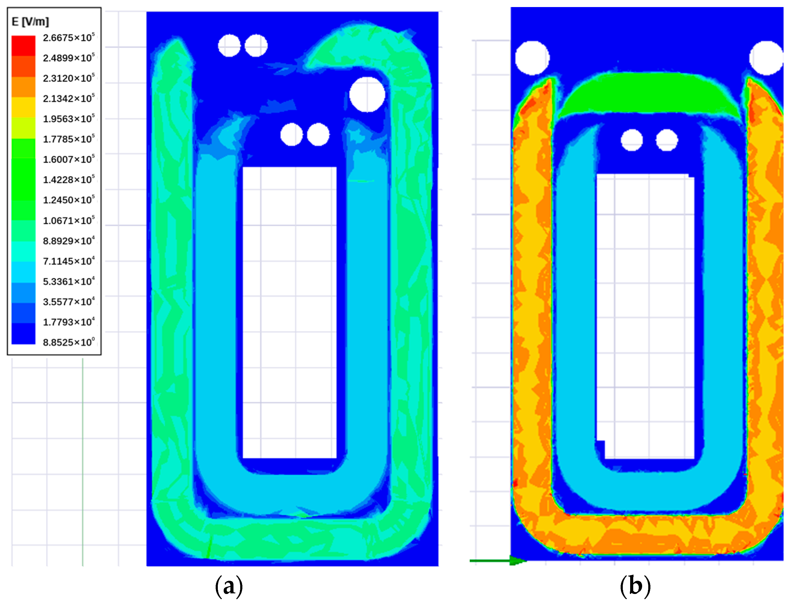
Figure 7 and Figure 8 shows the simulation results. According to the simulation, the simulated capacitance of the planar inductor winding using the traditional winding structure is 253.6 pF, while the simulated capacitance of the planar inductor winding using the interleaved winding structure is 116.5 pF. Therefore, the parasitic capacitance of the planar inductor winding using the interleaved winding structure is only 42% of that using the traditional winding structure, and the result is very close to the theoretical analysis calculation result in Section 3.1.
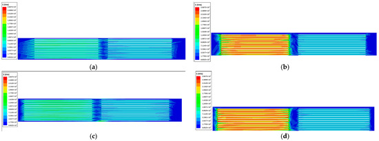
Figure 7.
Simulation results of the planar inductor: (a) interleaved winding inductor simulation result on ZY plane; (b) traditional wound inductor simulation result on ZY plane; (c) interleaved winding inductor simulation result on ZX plane; (d) traditional wound inductor simulation result on ZX plane.
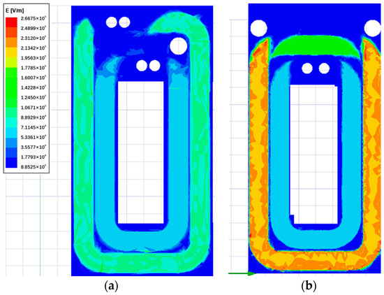
Figure 8.
Simulation results of the planar inductor: (a) interleaved winding inductor simulation result on XY plane; (b) traditional wound inductor simulation result on XY plane.
3.3. Summary
In this section, the FEM analysis of the electric field distribution and the simulated parasitic capacitance are presented. The FEM simulation can verify the theory that the planar inductor winding using the interleaved winding structure can significantly reduce the parasitic capacitance of the planar inductor compared with the traditional winding structure.
4. Experiment and Verification
In order to verify the effectiveness of the inductor design scheme, the traditional winding inductor and the interleaved winding inductor shown in Figure 9 were made by using flexible printed circuit boards. Both inductors had an inductance value of 2 μH and were composed of six flexible PCBs stacked and connected in parallel. Each flexible PCB was a two-layer board, and a single flexible PCB board formed a four-turn winding. The line width and line spacing were equal, and the samples are shown in Figure 10. Compared to constructing a multilayer planar inductor with either a 12-layer traditional PCB or six 2-layer traditional PCBs in parallel, employing flexible PCBs for validating the multilayer planar inductor design can significantly reduce the fabrication costs and cycle time for experimental samples. Additionally, it ensures alignment between the experimental samples and the FEM simulation model. The cores utilized were Ferroxcube E22 ferrite cores with a core material of 3F4, suitable for the design requirements of resonant inductors in resonant converters operating at switching frequencies from 10 kHz to 2 MHz. Considering the capacitance variation of resonant capacitors at high frequencies, ceramic capacitors made of NPO material, which are less affected by high frequencies, were selected. Taking into account the potential decrease in capacitance during the high-frequency operation of the LLC resonant converter, the actual resonant capacitors chosen were slightly higher than the designed resonant capacitance value. Forty IHHEC C1812N122J302T capacitors, which were manufactured by Holy Stone Enterprise Co., Ltd. (Taipei, Taiwan), each with a capacitance of 1.2 nF, were connected in parallel. Under the influence of high frequencies, specifically within 30 MHz, the actual resonant capacitance value was 40 nF.

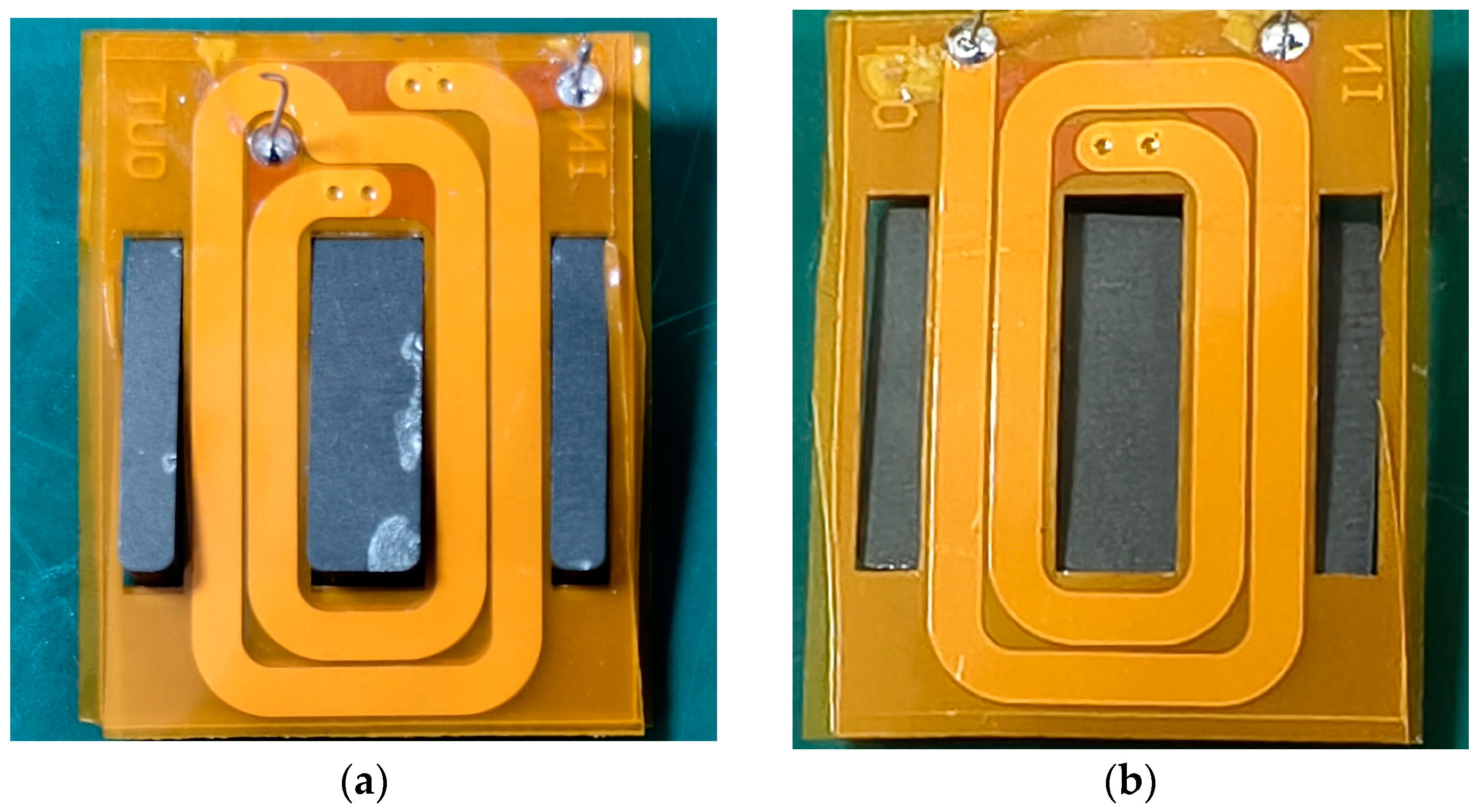
Figure 9.
Inductors for experiment: (a) interleaved winding planar inductor; (b) traditional winding planar inductor.
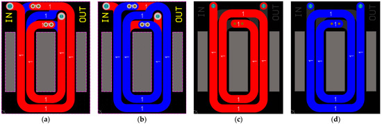
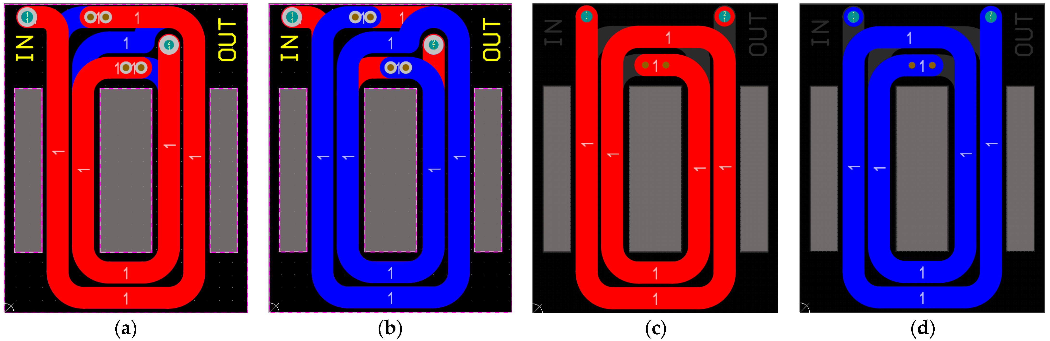
Figure 10.
The flexible PCB winding design of the inductors: (a) top layer design of the interleaved winding in the FPC board; (b) bottom layer design of the interleaved winding in the FPC board; (c) top layer design of the traditional winding in the FPC board; (d) bottom layer design of the traditional winding in the FPC board.
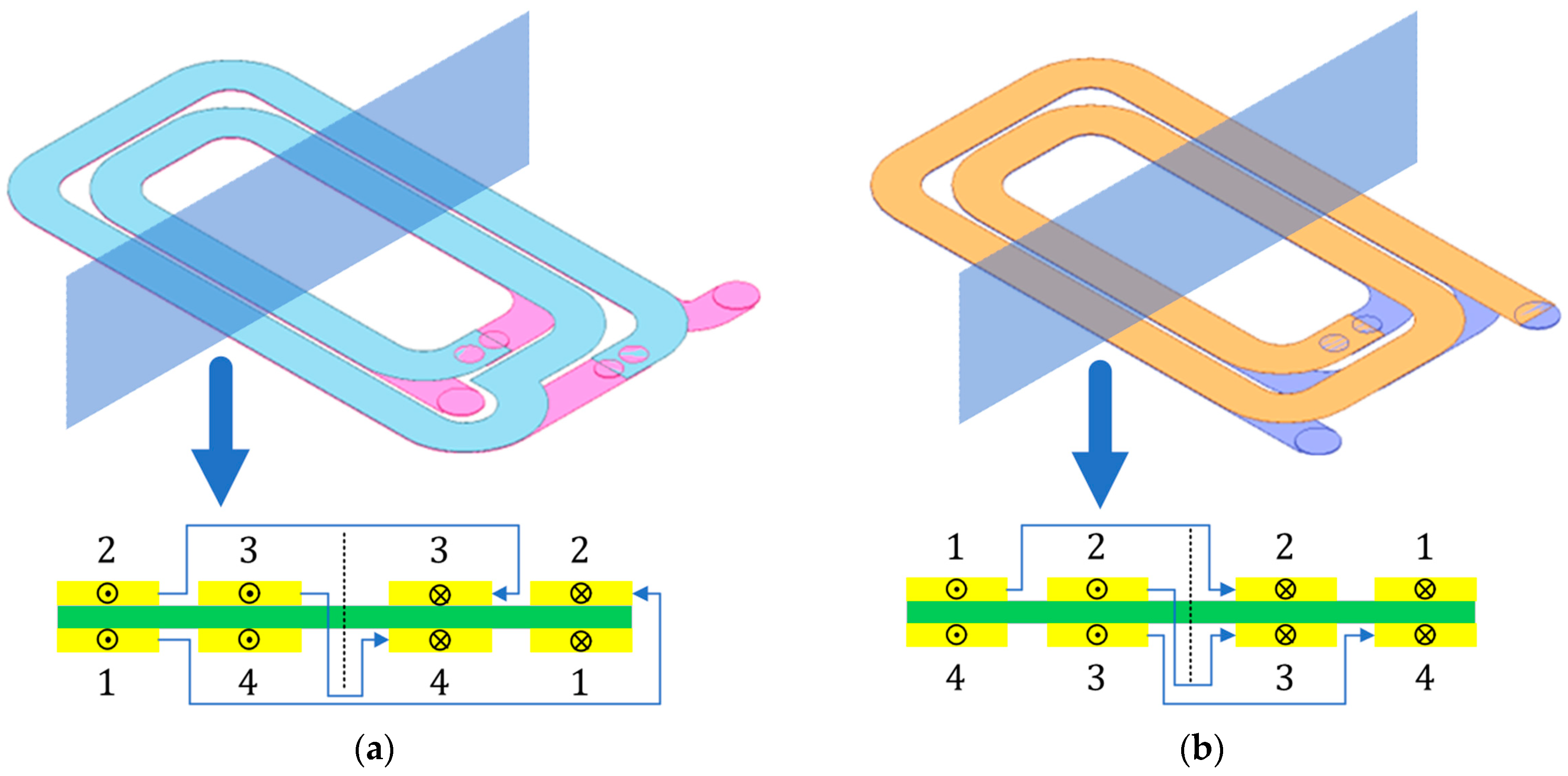
In order to verify the current ringing phenomenon of planar inductors, two planar transformers with different structures and the same excitation inductance and leakage inductance values were selected for comparative experiments. The two planar transformers were, respectively, a planar transformer, using two windings forming the primary and secondary windings, with a 4-layer PCB and a winding structure of P-S-S-P, and another planar transformer, using multiple windings in parallel with a 24-layer PCB and a winding structure of P-P-S-S. The cores used were Ferroxcube ER51 ferrite cores with core material of 3C95. The transformation ratio of the two planar transformers was 4:4, the structure of a single winding was the same, the excitation inductance values of the two transformers were the same, the leakage inductance values were 200 nH, and the prototypes are shown in Figure 11.
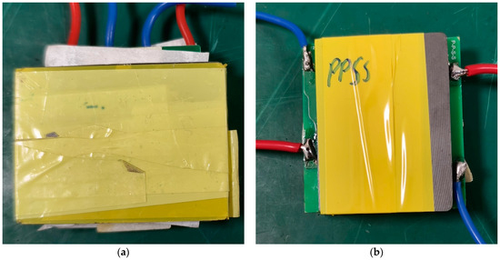
Figure 11.
Planar transformers for experiment: (a) 4-layer PCB planar transformer; (b) 24-layer PCB planar transformer.
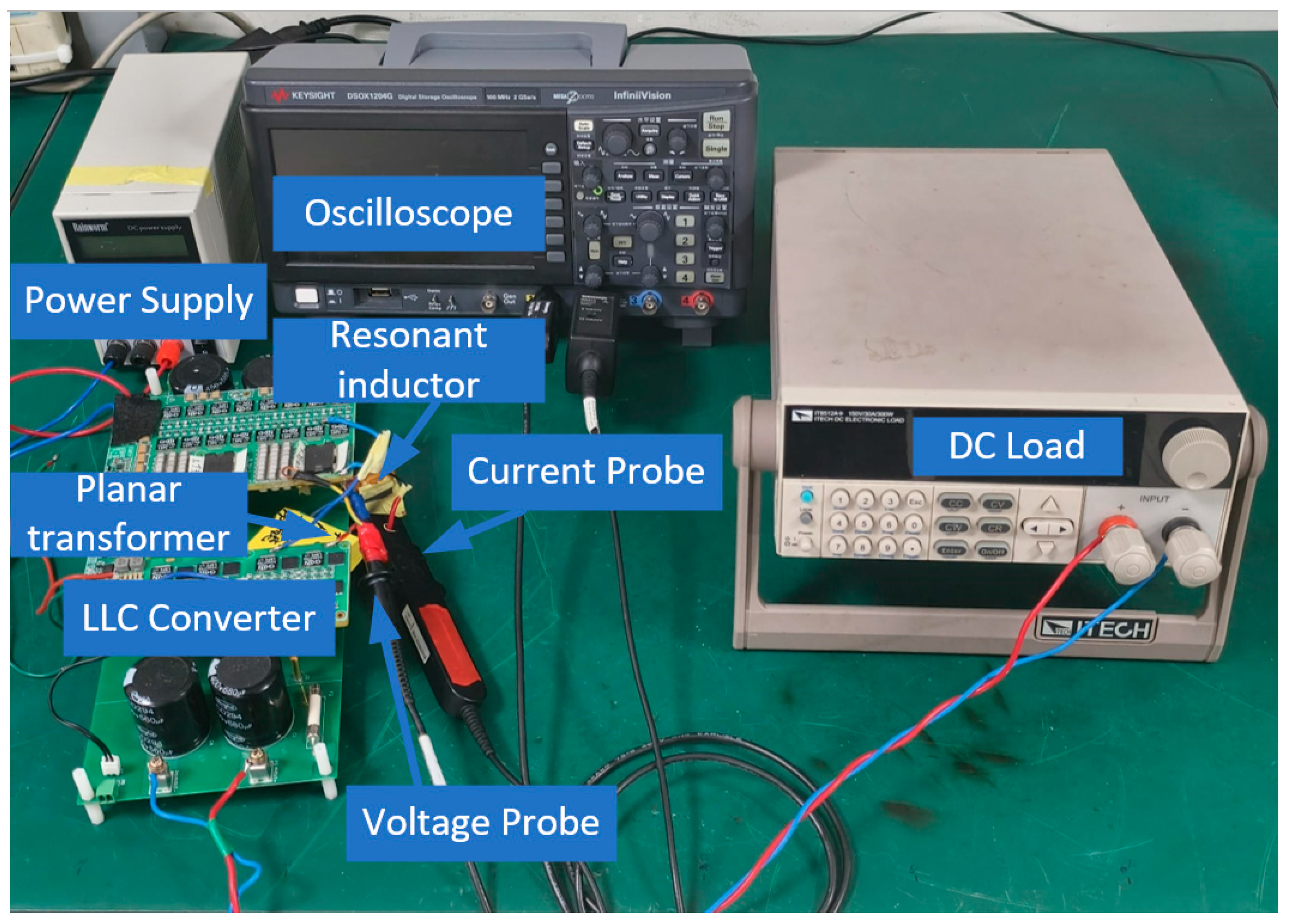
The method used to verify the current ringing was to build an LLC resonant converter test platform, under the same switching frequency test conditions, measure the resonant current waveform, measure the amplitude and frequency of the current ringing using different planar inductors and planar transformers, and measure the harmonic distortion of the resonant current. The experimental platform was built as shown in Figure 12, where the primary side of the experimental platform used a full-bridge circuit composed of GaN HEMTs with the GaN System GS66516B from GaN System, Ottawa, ON, Canada, which has the advantage of low loss, and the secondary side used a full-bridge rectifier circuit composed of diodes with Infineon IDL10G65C5. During the measurement, the voltage waveform and the resonant current waveform of the primary side of the converter were measured simultaneously. The current probe used was P6021A, manufactured by Tektronix. The voltage probe used was P5100A, manufactured by Tektronix. The oscilloscope used was DSOX1204G, from Keysight Technologies, Santa Rosa, CA, USA. The LLC resonant converter test platform used a controller with the TMSF280049C to generate the full-bridge circuit switch drive signal. The input voltage was set to 12 V, and by changing the load impedance, the resonant current with different peak-to-peak values could be obtained under different load impedance values, and the current ringing was measured. The resonant network consisted of the excitation inductor , the resonant inductor , and the resonant capacitor . The design parameters of the LLC resonant converter used by the test platform are shown in Table 1, where the resonant frequency of the LLC resonant converter was 565 kHz, the switching frequency was set to 450 kHz, and the switching dead time was set to 100 ns.

Figure 12.
LLC resonant converter experiment prototype for planar inductor testing.

Table 1.
System parameters.
4.1. Current Ringing of Resonant Current
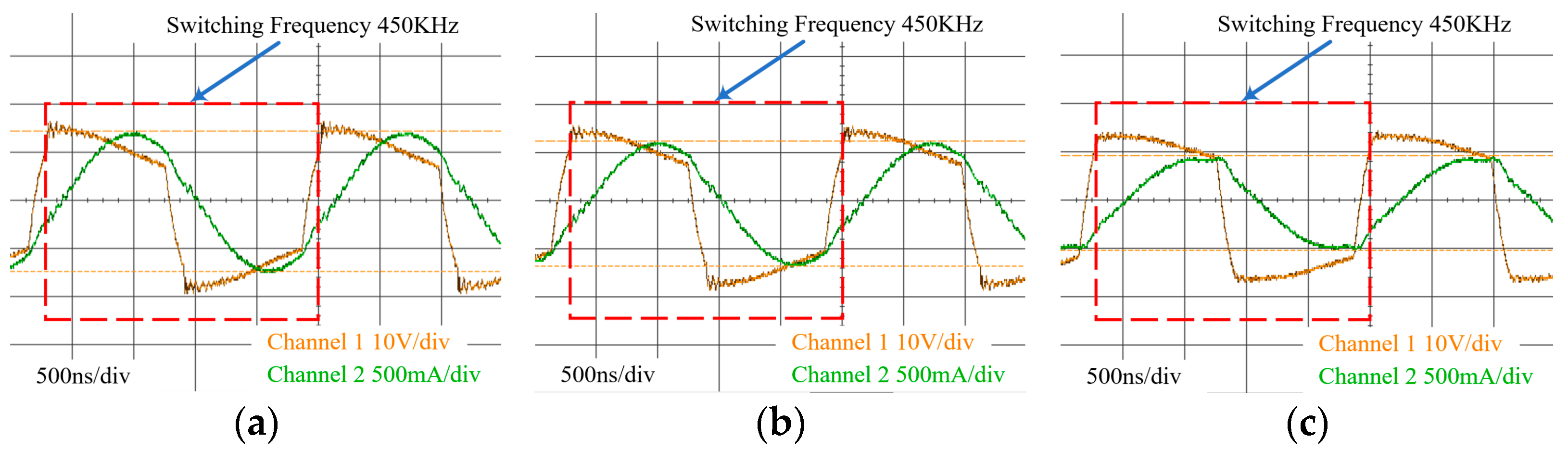
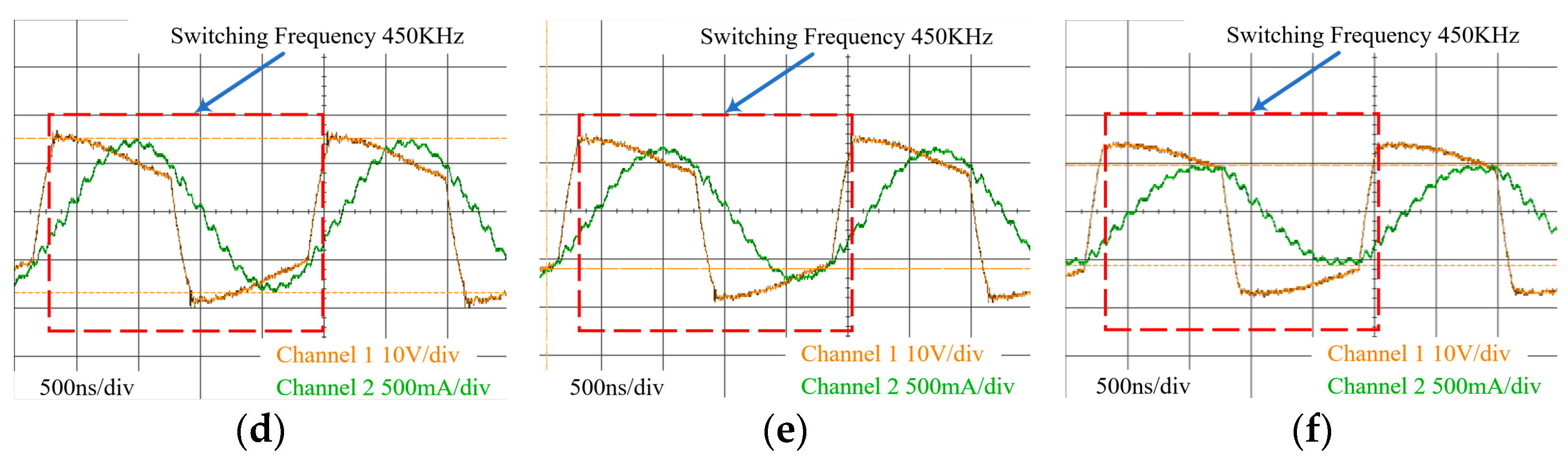
Using the planar transformer with a four-layer PCB, the load resistance value of the LLC resonant converter test platform was changed, and the comparison diagram of the measured resonant current waveform is shown in Figure 13. The waveform measured in channel 1 of the oscilloscope was the voltage waveform of the primary side, and the waveform measured in channel 2 was the resonant current waveform. Among them, Figure 13a–c are the resonant current waveforms obtained by using the traditional winding inductor, respectively, at loads of 25 Ω, 30 Ω, and 50 Ω. Figure 13d–f are the resonant current waveforms obtained by using the interleaved winding inductor, respectively, at loads of 25 Ω, 30 Ω, and 50 Ω. It can be observed from Figure 13 that under the same load conditions, compared with the LLC resonant converter using the traditional winding inductor, the interleaved winding inductor can reduce the current ringing of the resonant current.
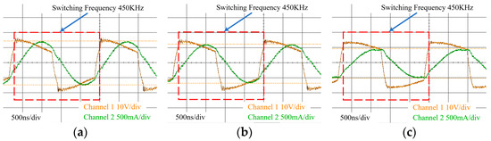
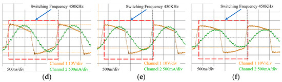
Figure 13.
Four-layer PCB planar transformer resonant current experiment results: (a) resonant current using interleaved winding planar inductor with 25 Ω load; (b) resonant current using interleaved winding planar inductor with 30 Ω load; (c) resonant current using interleaved winding planar inductor with 50 Ω load; (d) resonant current using traditional winding planar inductor with 25 Ω load; (e) resonant current using traditional winding planar inductor with 30 Ω load; (f) resonant current using traditional winding planar inductor with 50 Ω load.
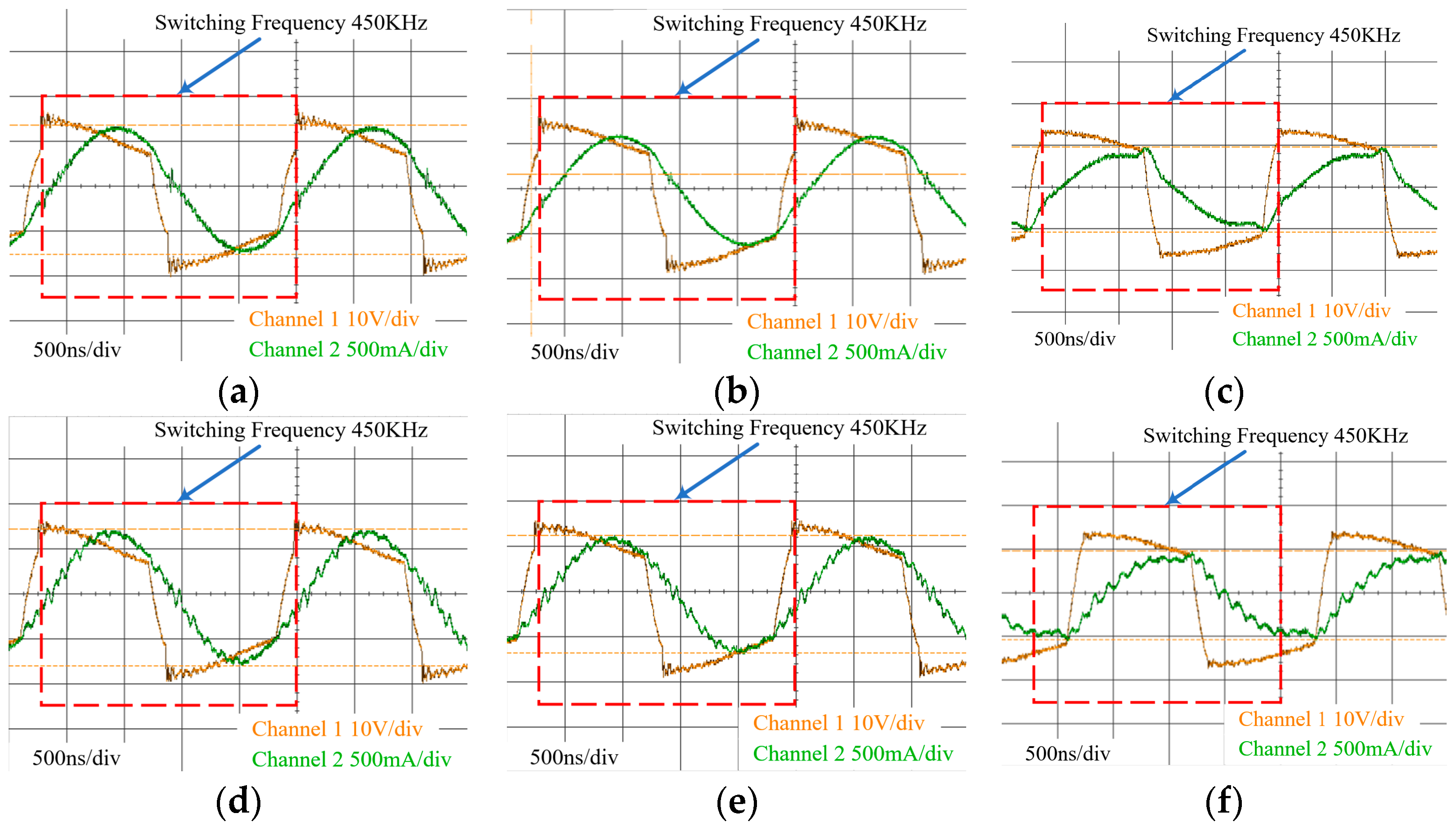
Using a planar transformer with a 24-layer PCB, changing the load resistance of the LLC resonant converter test platform, and the waveform comparison diagram obtained by measurement is shown in Figure 14. Figure 14a–c are the resonant current waveforms obtained by using the traditional winding inductor, respectively, at loads of 25 Ω, 30 Ω, and 50 Ω. Figure 14d–f are the resonant current waveforms obtained by using the interleaved winding inductor, respectively, at loads of 25 Ω, 30 Ω, and 50 Ω. From Figure 14, the same experimental phenomenon as in Figure 13 can be observed, which, using the interleaved winding inductor, can reduce the current ringing.
Figure 14.
Twenty-four-layer PCB planar transformer resonant current experiment results: (a) resonant current using interleaved winding planar inductor with 25 Ω load; (b) resonant current using interleaved winding planar inductor with 30 Ω load; (c) resonant current using interleaved winding planar inductor with 50 Ω load; (d) resonant current using traditional winding planar inductor with 25 Ω load; (e) resonant current using traditional winding planar inductor with 30 Ω load; (f) resonant current using traditional winding planar inductor with 50 Ω load.
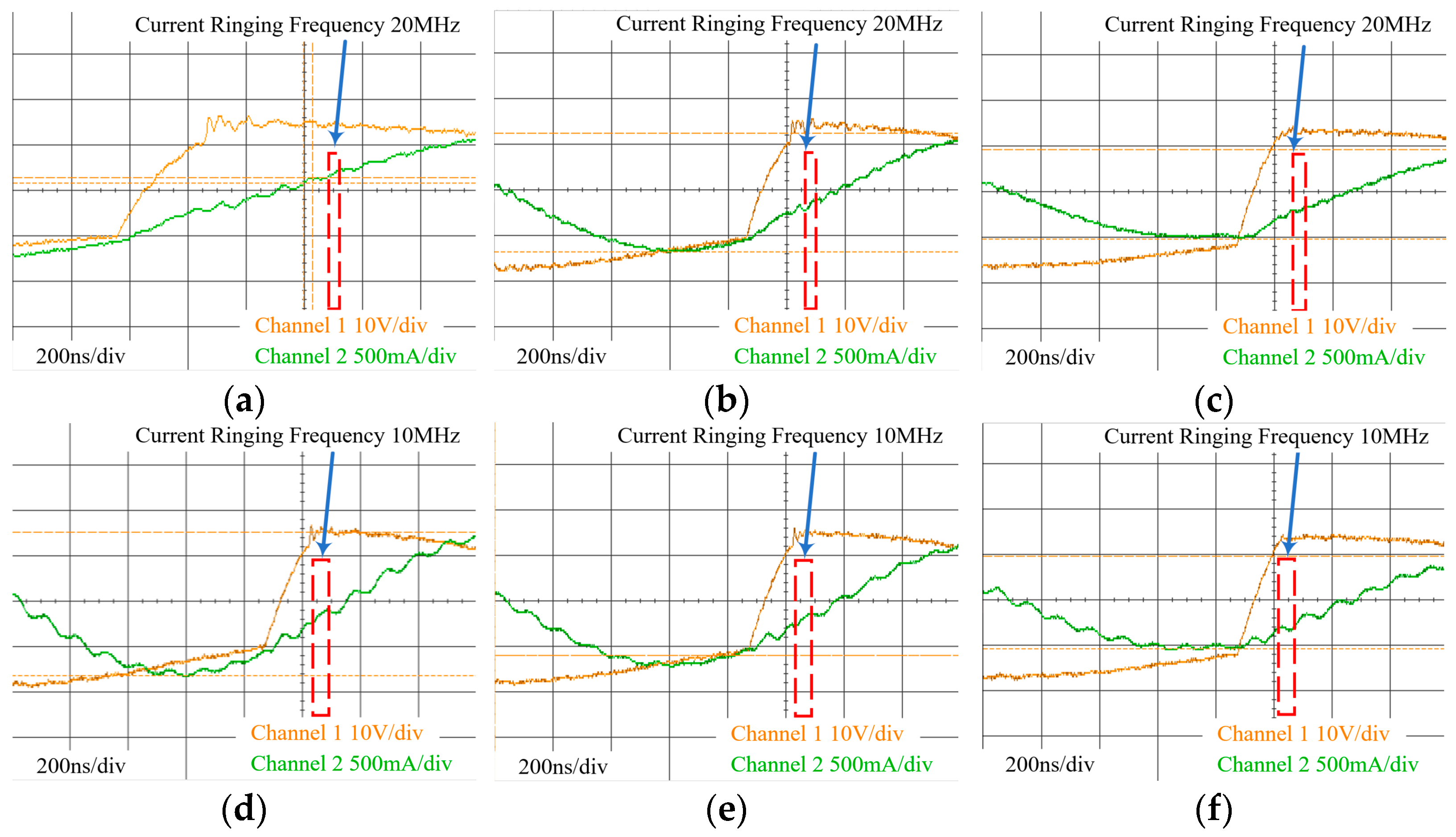
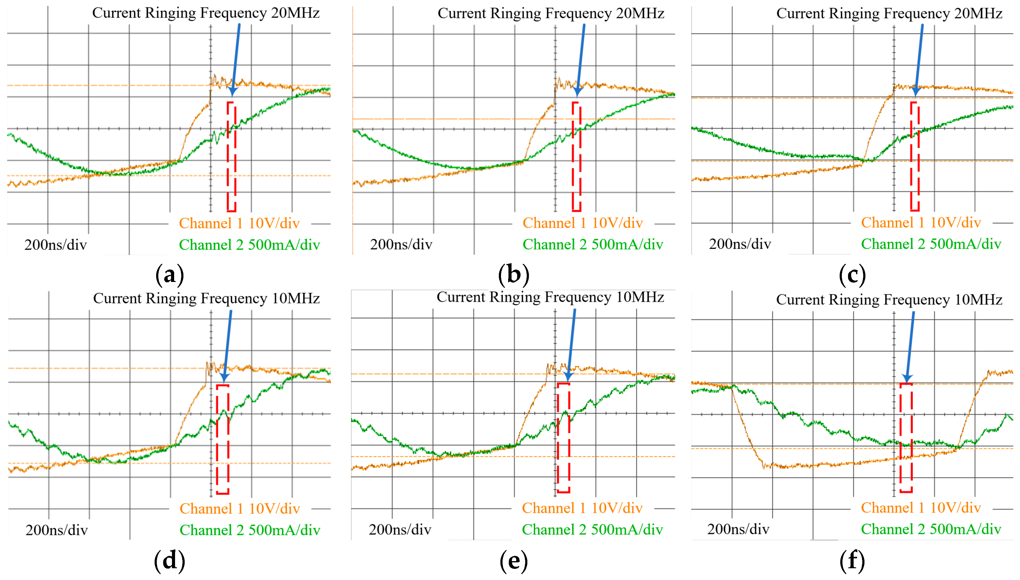
By reducing the time division value of the oscilloscope measurement from 500 ns/div to 200 ns/div, we obtain Figure 15 and Figure 16 based on Figure 13 and Figure 14. From Figure 15 and Figure 16, the current ringing amplitude and frequency can be measured, and the current ringing amplitude is shown in Table 2. From the data results in Table 2, it can be seen that compared with the planar inductor with conventional winding, the planar inductor with interleaved winding has a lower current ringing amplitude. From Figure 15 and Figure 16, it can be observed that the waveform results obtained by using the interleaved winding inductor, as shown in Figure 15a–c and Figure 16a–c, have a current ringing frequency of 20 MHz, and the measurement results using the traditional winding inductor, as shown in Figure 15d–f and Figure 16d–f, have a current ringing frequency of 10 MHz. By measuring Figure 15 and Figure 16, the current ringing amplitude of the resonant current can be obtained, as shown in Table 2. Combining the experimental results shown in Figure 15 and Figure 16, and Table 2, it can be seen that using the interleaved winding inductor, compared with the traditional winding inductor, can reduce current ringing.
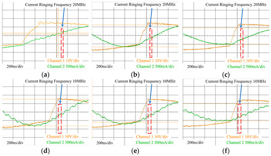
Figure 15.
Four-layer PCB planar transformer resonant current ringing measurement. (a) resonant current using interleaved winding planar inductor with 25 Ω load; (b) resonant current using interleaved winding planar inductor with 30 Ω load; (c) resonant current using interleaved winding planar inductor with 50 Ω load; (d) resonant current using traditional winding planar inductor with 25 Ω load; (e) resonant current using traditional winding planar inductor with 30 Ω load; (f) resonant current using traditional winding planar inductor with 50 Ω load.
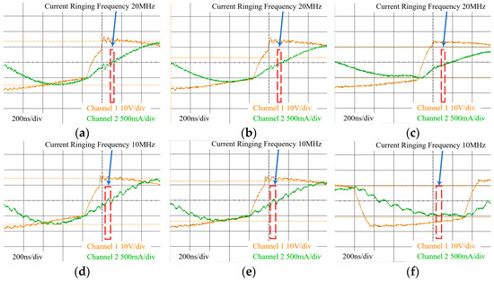
Figure 16.
Twenty-four-layer PCB planar transformer resonant current ringing measurement. (a) resonant current using interleaved winding planar inductor with 25 Ω load; (b) resonant current using interleaved winding planar inductor with 30 Ω load; (c) resonant current using interleaved winding planar inductor with 50 Ω load; (d) resonant current using traditional winding planar inductor with 25 Ω load; (e) resonant current using traditional winding planar inductor with 30 Ω load; (f) resonant current using traditional winding planar inductor with 50 Ω load.
Table 2.
Resonant current peak-to-peak value and current ringing measurement.
4.2. Measurement of THD of Resonant Current
According to the measurement results of Figure 8, Figure 9, Figure 10 and Figure 11, the harmonic distortion of the measured resonant current waveform was measured, and the results are shown in Table 3. From Table 3, it can be seen that under different conditions of planar transformers and loads, the harmonic distortion of the resonant current using the interleaved winding inductor was smaller than that using the conventional winding inductor. Therefore, using the interleaved winding inductor can reduce harmonic distortion.
Table 3.
Resonant current THD value.
4.3. Comparison of Different Inductor Designs
In this paper, FEM simulation models for both the interleaved winding planar inductor and the traditional winding planar inductor were established. Two types of inductors were fabricated and tested in an LLC resonant converter prototype. Theoretical calculations and simulations demonstrated that, with the same length of the outer turn of the winding, the interleaved winding planar inductor exhibits a smaller parasitic capacitance. This was experimentally validated, showing that the interleaved winding planar inductor has reduced current ringing compared to traditional winding planar inductor in the LLC resonant converter prototype. Therefore, under identical winding design parameters, the interleaved winding planar inductor not only shares the same manufacturing cost with the traditional winding planar inductor but also offers a smaller parasitic capacitance, leading to reduced ringing current when applied to LLC resonant converters.
Commonly used in power converters, toroidal inductors reduce electromagnetic interference (EMI) but cannot eliminate it entirely. Toroidal inductors are costly to manufacture and complex to install. Unable to be produced as planar structures, toroidal inductors fail to meet the miniaturization needs of power converters, which makes it difficult to reduce their size for power converters with high power density. Therefore, after a comprehensive comparison of toroidal inductors and traditional winding inductors, considering cost, installation, and the effect on suppressing current ringing, this paper proposes that the interleaved winding inductor is the best design.
5. Conclusions
This paper analyzes the causes of current ringing in LLC resonant converters. A resonant tank impedance model is established. Through the impedance model, it is found that the parasitic capacitance of the resonant inductor causes current ringing, and the method to reduce the current ringing is to reduce the parasitic capacitance of the resonant inductor. In addition, based on the planar conductor parasitic capacitance model, an interleaved winding design method for multilayer planar inductors is proposed, which reduces the parasitic capacitance of the inductor winding by reducing the voltage difference between the upper and lower adjacent layers, without changing the design requirement of the inductor winding width. FEM simulations and experimental validation demonstrated that the interleaved winding inductor exhibits a significantly lower parasitic capacitance compared to the traditional winding inductor. With the same design parameters, the parasitic capacitance of the interleaved winding inductor was only 42% of that of the traditional winding inductor. The LLC resonant converter utilizing the interleaved winding inductor showed a 60% reduction in current ringing amplitude under various loads and, consequently, the total harmonic distortion (THD) was reduced by 1%. Compared with a traditionally wound inductor, interleaved winding does not increase the additional manufacturing cost and complexity under the design requirement of high power density. The use of interleaved winding inductors can reduce the current ringing of LLC resonant converters, as well as the harmonic distortion of the converters. Therefore, the use of interleaved winding inductors is beneficial for the design of LLC resonant converters.
Author Contributions
Conceptualization, Q.L.; methodology, Q.L.; validation, Q.L. and Z.Z.; writing—original draft preparation, Q.L.; writing—review and editing, Q.L. All authors have read and agreed to the published version of the manuscript.
Funding
This research was funded by the Key Laboratory of High Power Microwave Technology Fund Project at Southwest Jiaotong University under Grant HPM2204.
Data Availability Statement
The original contributions presented in the study are included in the article, further inquiries can be directed to the corresponding author.
Conflicts of Interest
The authors declare no conflicts of interest.
References
- Fei, C.; Gadelrab, R.; Li, Q.; Lee, F.C. High-Frequency Three-Phase Interleaved LLC Resonant Converter with GaN Devices and Integrated Planar Magnetics. IEEE J. Emerg. Sel. Top. Power Electron. 2019, 7, 653–663. [Google Scholar] [CrossRef]
- Serban, E.; Saket, M.A.; Ordonez, M. High-Performance Isolated Gate-Driver Power Supply with Integrated Planar Transformer. IEEE Trans. Power Electron. 2021, 36, 11409–11420. [Google Scholar] [CrossRef]
- Hammer, J.; Saket, M.A.; Ordonez, M. LLC Converters with GaN: Commutation Loop Capacitance. In Proceedings of the 2022 IEEE Applied Power Electronics Conference and Exposition (APEC), Houston, TX, USA, 20–24 March 2022; pp. 1752–1756. [Google Scholar]
- Qin, Z.; Shen, Z.; Blaabjerg, F.; Bauer, P. Modelling, Analysis and Mitigation of the Transformer Current Ringing in Dual Active Bridge Converters. In Proceedings of the 2018 IEEE Energy Conversion Congress and Exposition (ECCE), Portland, OR, USA, 23–27 September 2018; pp. 650–655. [Google Scholar]
- Saket, M.A.; Ordonez, M.; Craciun, M.; Botting, C. Improving Planar Transformers for LLC Resonant Converters: Paired Layers Interleaved. IEEE Trans. Power Electron. 2019, 34, 11813–11832. [Google Scholar] [CrossRef]
- Kitagawa, W.; Kutsuna, T.; Kuwana, K.; Kawamura, Y.; Takeshita, T. Conducted Noise Simulation on AC–DC Converter Using SiC-MOSFET. IEEE Trans. Ind. Appl. 2021, 57, 1644–1651. [Google Scholar] [CrossRef]
- Kim, K.-W.; Jeong, Y.; Kim, J.-S.; Moon, G.-W. Low Common-Mode Noise Full-Bridge LLC Resonant Converter with Balanced Resonant Tank. IEEE Trans. Power Electron. 2021, 36, 4105–4115. [Google Scholar] [CrossRef]
- Shen, Z.; Wang, H.; Shen, Y.; Qin, Z.; Blaabjerg, F. An Improved Stray Capacitance Model for Inductors. IEEE Trans. Power Electron. 2019, 34, 11153–11170. [Google Scholar] [CrossRef]
- Qin, Z.; Shen, Z.; Blaabjerg, F.; Bauer, P. Transformer Current Ringing in Dual Active Bridge Converters. IEEE Trans. Ind. Electron. 2021, 68, 12130–12140. [Google Scholar] [CrossRef]
- Gajardo, M.L.; Gomez, P.I.; Mijatovic, N.; Perez, J.R.; Dragicevic, T. Generalized Data-Driven Model to Minimize Current Ringing in DAB Power Converter. IEEE J. Emerg. Sel. Top. Ind. Electron. 2024, 5, 126–137. [Google Scholar] [CrossRef]
- Nguyen, M.H.; Fortin Blanchette, H. A Review and Comparison of Solid, Multi-Strands and Litz Style PCB Winding. Electronics 2020, 9, 1324. [Google Scholar] [CrossRef]
- Lope, I.; Carretero, C.; Acero, J. First Self-Resonant Frequency of Power Inductors Based on Approximated Corrected Stray Capacitances. IET Power Electron. 2021, 14, 257–267. [Google Scholar] [CrossRef]
- Zhao, H.; Yan, Z.; Luan, S.; Dalal, D.N.; Jørgensen, J.K.; Wang, R.; Zhou, X.; Bęczkowski, S.M.; Rannestad, B.; Munk-Nielsen, S. A Comparative Study on Parasitic Capacitance in Inductors with Series or Parallel Windings. IEEE Trans. Power Electron. 2022, 37, 15140–15151. [Google Scholar] [CrossRef]
- Kolahian, P.; Grimm, F.; Baghdadi, M. A Comprehensive Review on Planar Magnetics and the Structures to Reduce the Parasitic Elements and Improve Efficiency. Energies 2023, 16, 3254. [Google Scholar] [CrossRef]
- Kharanaq, F.A.; Emadi, A.; Bilgin, B. Modeling of Conducted Emissions for EMI Analysis of Power Converters: State-of-the-Art Review. IEEE Access 2020, 8, 189313–189325. [Google Scholar] [CrossRef]
- Li, C.; Ma, Q.; Tong, Y.; Wang, J.; Xu, P. A Survey of Conductive and Radiated EMI Reduction Techniques in Power Electronics Converters across Wide-Bandgap Devices. IET Power Electron. 2023, 16, 2121–2137. [Google Scholar] [CrossRef]
- Yuan, L.; Zhang, J.; Liang, Z.; Hu, M.; Chen, G.; Lu, W. EMI Challenges in Modern Power Electronic-Based Converters: Recent Advances and Mitigation Techniques. Front. Electron. 2023, 4, 1274258. [Google Scholar] [CrossRef]
- Wu, X.; Gao, X.; Wang, J.; Li, Z.; Du, S.; Gao, S.; Li, F.; Du, J.; Shchurov, N.I.; Zhang, X. Advances in Modeling and Suppression Methods of EMI in Power Electronic Converters of Third-Generation Semiconductor Devices. Electronics 2023, 12, 2348. [Google Scholar] [CrossRef]
- Ferreira, J.A. Improved Analytical Modeling of Conductive Losses in Magnetic Components. IEEE Trans. Power Electron. 1994, 9, 127–131. [Google Scholar] [CrossRef]
- Hurley, W.G.; Wolfle, W.H. Transformers and Inductors for Power Electronics; Wiley: Hoboken, NJ, USA, 2013. [Google Scholar]


Disclaimer/Publisher’s Note: The statements, opinions and data contained in all publications are solely those of the individual author(s) and contributor(s) and not of MDPI and/or the editor(s). MDPI and/or the editor(s) disclaim responsibility for any injury to people or property resulting from any ideas, methods, instructions or products referred to in the content. |
© 2024 by the authors. Licensee MDPI, Basel, Switzerland. This article is an open access article distributed under the terms and conditions of the Creative Commons Attribution (CC BY) license (https://creativecommons.org/licenses/by/4.0/).