Article

Orthogonal-Frequency Simultaneous Wireless Power and Data Transfer for High-Power Wireless EV Charging

College of Electrical Engineering, Zhejiang University, Hangzhou 310027, China
*
Author to whom correspondence should be addressed.
Energies 2024, 17(8), 1851; https://doi.org/10.3390/en17081851
Submission received: 7 March 2024 / Revised: 27 March 2024 / Accepted: 10 April 2024 / Published: 12 April 2024
(This article belongs to the Section E: Electric Vehicles)

Abstract

:
In a simultaneous wireless power and data transfer (SWPDT) system using common coils, achieving high-speed communication in high-power wireless charging systems is challenging due to power transfer interference on communication. Based on high-frequency data carrier-based SWPDT (HFDC-SWPDT) technology, this paper proposes an orthogonal-frequency simultaneous wireless power and data transfer (OF-SWPDT) method to minimize interference where the data carrier frequency is orthogonal to the power carrier frequency and its harmonics. In addition, a guard band is inserted between the spectra of power harmonics and data in order to further separate the power and data spectra. Thus, a high-power, high-speed SWPDT system is achieved. Finally, an 11 kW prototype with 64.125 kbps full-duplex communication is developed to validate the proposed method.

1. Introduction

Wireless power transfer (WPT) is an emerging charging technique with the advantages of convenience, safety, and reliability for electrical vehicles (EVs). Compared with wired chargers, wireless EV chargers (WEVCs) eliminate the need for power cable connections, reducing the risk of handling high-power cables, especially in poor weather conditions [1,2].
In practical WPT systems, communication between primary and secondary sides is generally required for feedback control [3], state monitoring [4], alignment of coils [5], vehicle identification [6], etc. Conventional radio-frequency (RF) communication solutions, such as Wi-Fi and Bluetooth, are hampered by long transmission delays, troublesome pairing processes, and transmission security issues. To solve these problems, various simultaneous wireless power and data transfer (SWPDT) technologies have been proposed and investigated [7].
SWPDT techniques can be categorized into two groups based on whether power and data are transmitted through the same channel: power and data transfer through a single channel (SC-SWPDT) and multiple channels (MC-SWPDT) [7]. SC-SWPDT can further be divided into two categories: power carrier-based SWPDT (PC-SWPDT) and high-frequency data carrier-based SWPDT (HFDC-SWPDT). In the PC-SWPDT system, the data signal is generated by directly modulating the power signal [8,9]. In HFDC-SWPDT, the modulated data signal is injected into the common channel by using frequency-division multiplexing (FDM) [10,11,12,13,14,15,16,17,18,19,20]. MC-SWPDT can further be divided into two parts: the multiple inductive channel SWPDT system (MIC-SWPDT) by adding extra coil pairs for data transfer, and the inductive–capacitive hybrid channel SWPDT system (ICHC-SWPDT) by utilizing hybrid fields for SWPDT [21,22,23].
Among the aforementioned technologies, high-frequency data carrier-based SWPDT (HFDC-SWPDT) is gaining popularity due to its flexibility and reliability. In HFDC-SWPDT, the data are injected into the common channel through inductive or capacitive coupling [11,12,13,14,15]. Because power and data transmission share common coils, this method offers advantages in terms of size and cost. However, in high-power applications like WEVCs, significant cross-talk interference between data transmission and power transfer may occur, limiting its current feasibility to low and medium power levels.
Several methods have been investigated to suppress the cross-talk interference. The signal-to-noise ratio (SNR) is an indicator for assessing communication quality, and conventionally, two strategies are employed to increase the SNR.
The first strategy is to enhance data transmission gain. In [10], an extra-resonant tank for data communication was built to maximize the data transmission gain. A dual-resonant structure is proposed in [16,17] to improve the data transmission gain, but it can only realize half-duplex communication. In [18], a four-resonance dual-rejection structure was proposed, enhancing the gain and enabling full-duplex communication. In [19,20], the transfer function of the data channel is investigated to choose the optimal data carrier frequency for maximizing data transmission gain. The second strategy is to reduce interference from the power link. Bandpass or high-pass filters are applied to the data receiver to reduce the fundamental component and high-order harmonics of the power carrier [5,12]. The notch filter is an effective structure that can reduce cross-talk interference [11].
These solutions focus on enhancing the SNR in circuit designs. However, the spectrum interference from the power harmonics, whose frequencies are very close to those of data carriers, cannot be removed by filters.
To solve this problem, an orthogonal-frequency SWPDT (OF-SWPDT) technique is proposed in this paper. An 11 kW WPT system was built to verify the feasibility of achieving full-duplex high-speed communication in high-power applications. The main innovations and contributions of this study are summarized as follows:
  • This paper proposes an OF-SWPDT technique that eliminates spectrum interference from power harmonics. By optimizing the carrier frequency and bandwidth, the SNR of the communication channel is enhanced, enabling higher transmission power. A 64.125 kbps communication link is achieved in an 11 kW WPT system, which demonstrates the possibility of achieving full-duplex high-speed communication in high-power applications.
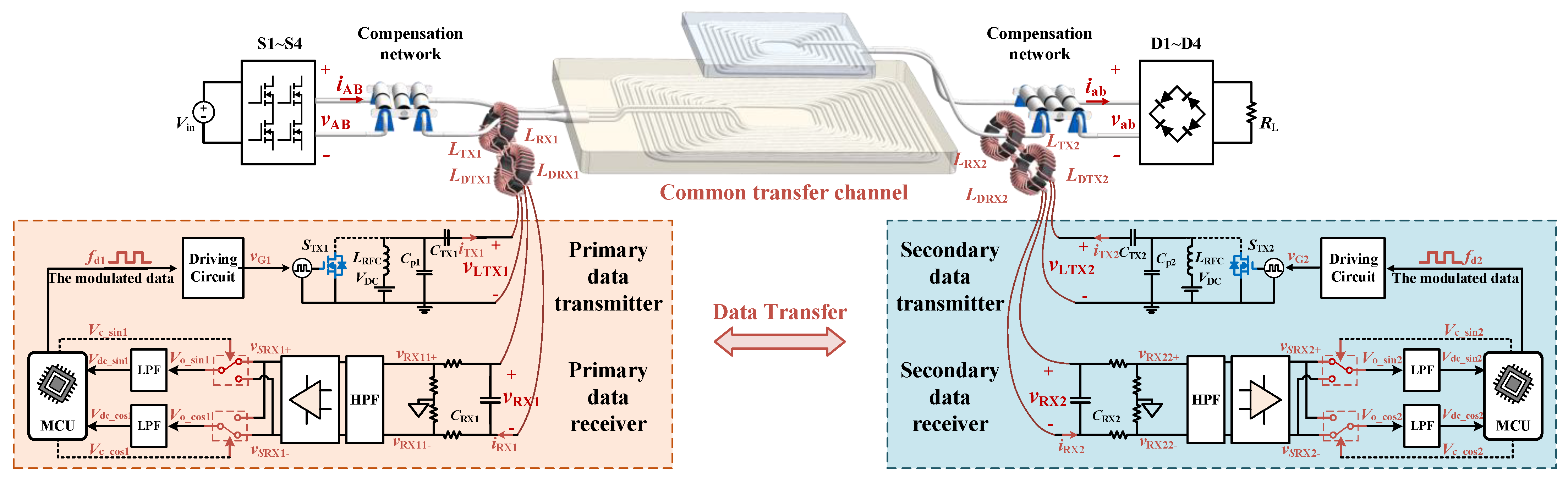
  • A plug-and-play toroidal transformer is proposed to inject and extract data carriers simultaneously, simplifying installation and facilitating migration to various WPT systems. Data can be correctly transferred without adding additional wave trappers to the WPT system.

2. Principle of the OF-SWPDT Technique

In a WPT system with a full bridge inverter, which is periodically operated, the power carrier and its harmonics can be expressed as follows:
v p ( t ) = k = 1 , 3 , 5 , A k cos ( 2 π k f p t + φ k ) ,
where fp is the frequency of the power carrier, and Ak and φk are the amplitude and initial phase of the kth harmonics, respectively. Note that there are no even harmonics in the power carrier.
To minimize the interference from the power carrier and its harmonics, this paper proposes an OF-SWPDT method. The primary goal of the method is to ensure that the data carriers are orthogonal to the power carrier and harmonics during a data symbol in communication, which satisfies the following equation at an arbitrary φd:
t t + T s v p ( t ) A d cos ( 2 π f d t + φ d ) d t = 0 ,
where Ad, fd, and φd are the amplitude, frequency, and initial phase of the data carrier, respectively, and Ts is the data symbol duration. From (1) and (2), the following can be derived:
{ f d = m 2 T s , k f p = n 2 T s ( m N + , n N + , k = 1 , 3 , 5 ) Δ f = | f d k f p | = j T s ( j N + , k = 1 , 3 , 5 ) .
To fulfill (3), a straightforward solution is to choose the carrier frequency as even multiples of the power carrier. Thus, fp, fd, and Ts satisfy the following relations:
{ f d = k d f p ( k d = 2 , 4 , 6 ) T s = k s T p = k s f p ( k s N + ) .
Given that the power wave is a square wave, the expressions of the power and data carriers’ spectra, Fpc(f) and Fdc(f), can be derived as follows:
{ F p c ( f ) = 4 V i n π k = 1 , 3 , 5 δ [ f k f p ] k F d c ( f ) = A d T s sin ( π T s ( f k d f p ) ) π T s ( f k d f p ) ( k d = 2 , 4 , 6 .... ) ,
where δ represents the unit impulse function. The spectra of the power harmonics and data carriers are shown in Figure 1. The symbol duration period Ts is set to 1/fp and 4/fp, respectively. The spectra that are covered with solid color blocks are the main lobes, and the rest of the spectra are the side lobes, in which the frequency ranges of the main lobes are called the carrier bandwidths. The bandwidths of the data carriers are determined by the symbol duration and can be expressed as 2/Ts.
In Figure 1a, it can be observed that the spectra of the power harmonics overlap with the main lobe of the data carrier. Theoretically, the power harmonic spectra are pulses and orthogonal with the data carrier spectrum; thus, the communication will not be impacted by the power harmonics. However, the orthogonal relationship between data carriers and power harmonics cannot be met if the power carrier frequency deviates slightly from the specified value. The dynamic characteristics of the WPT systems, such as frequency jitter within a close-loop controlling period, can destroy the orthogonal relationship. Therefore, it is preferable to narrow the main lobes of the data carrier by extending the symbol duration; consequently, a band-guard interval is established between the data carriers and power harmonics, as shown in Figure 1b, where the symbol duration Ts = 4/fp.
In conclusion, OF-SWPDT needs the fulfillment of the following two requirements:
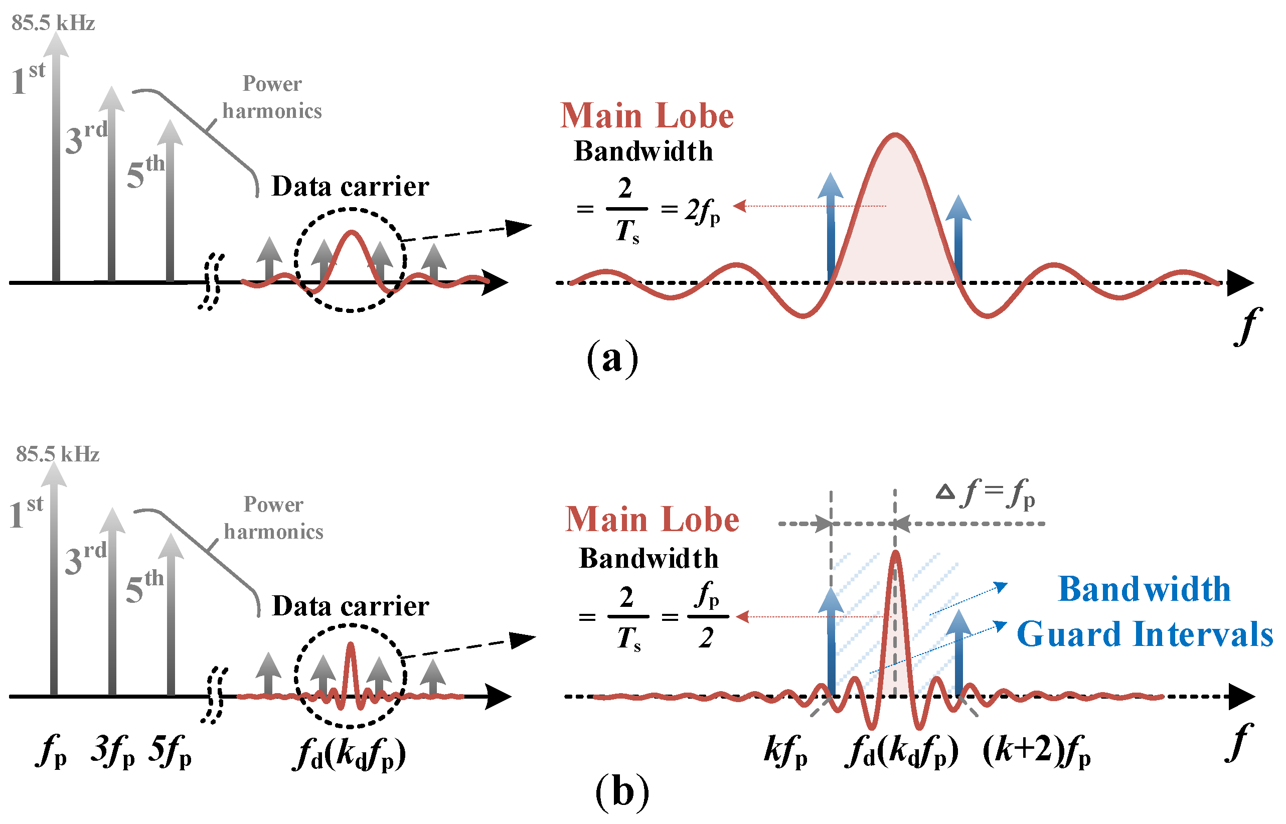
  • The frequency of the data carrier (fd) is an even integer multiple (kd) of the fundamental frequency of the power carrier (fp).
  • The symbol duration Ts is an integer multiple (ks) of the fundamental period of the power carrier (1/fp).

3. Analysis of Data Transmission

The structure of the proposed OF-SWPDT system is shown in Figure 2, which demonstrates that the forward and backward data transmissions are completely symmetrical. Subscripts “1” and “2” are used to distinguish the primary and secondary sides. And the backward data transmission is taken as an instance in this section.

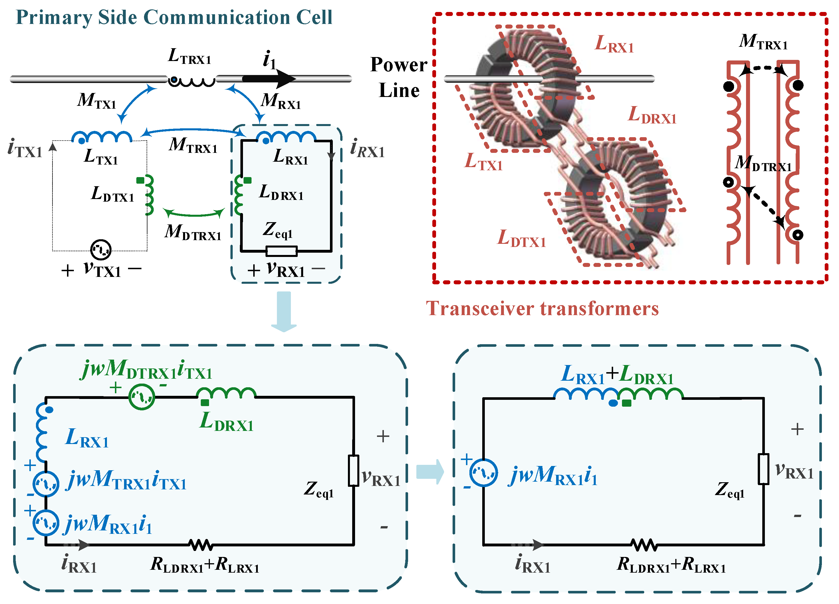
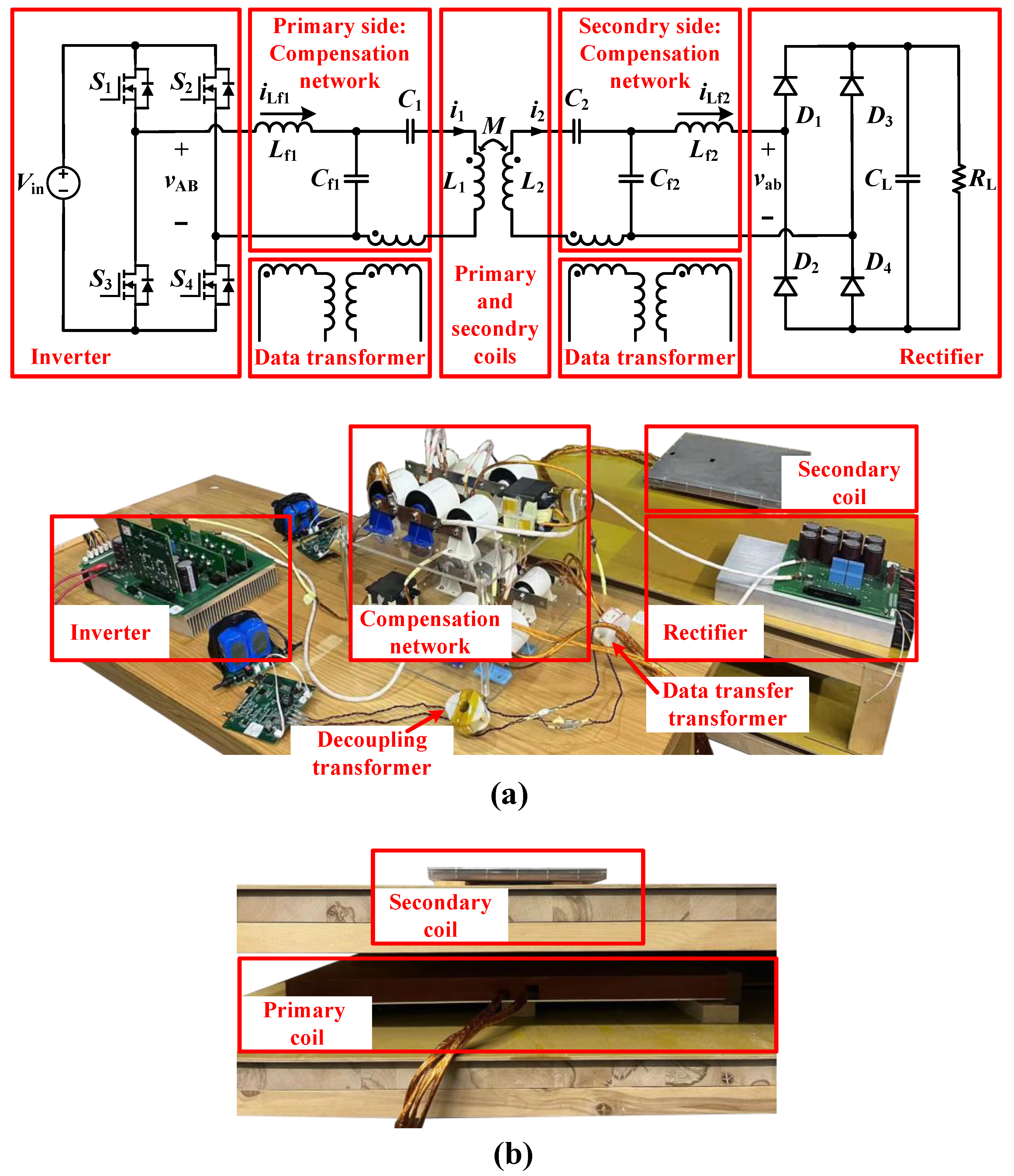
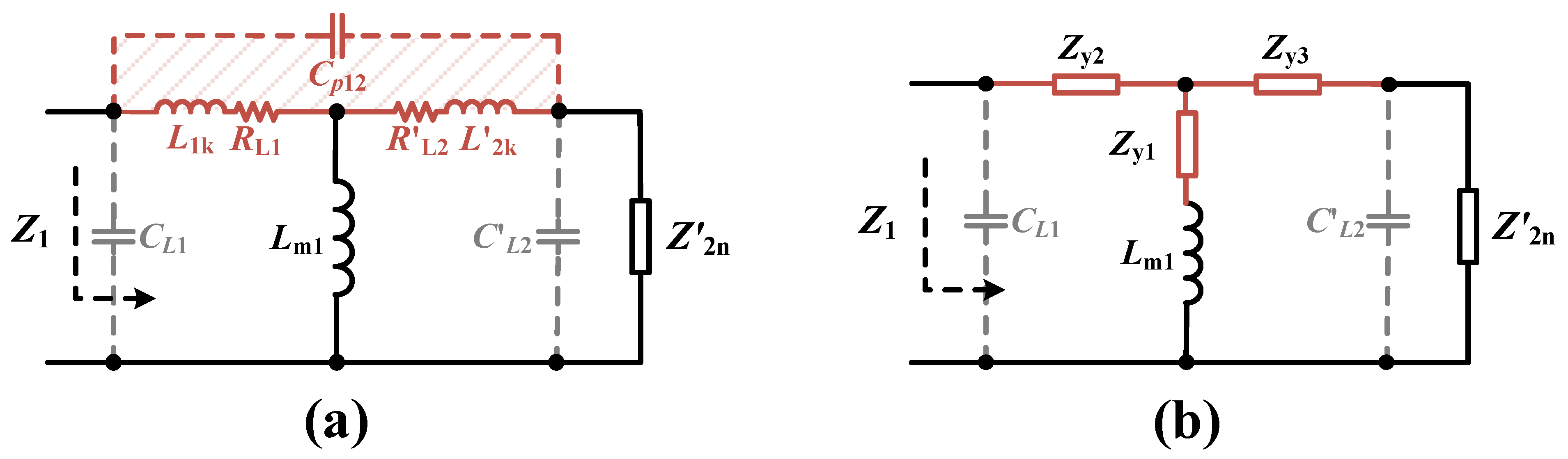
3.1. Structure of Plug-and-Play Toroidal Transformer

To eliminate the interference between the data-injecting inductor and the data-extracting inductor, a decoupling transformer is proposed in this paper. As is shown in Figure 3, the data carriers are injected into and extracted from the power channel via a pair of transceiver transformers. Each of the pairs of transceiver transformers has a toroidal core and two coils, one for transmitting and one for receiving. The two transmitting coils are connected serially in phase, whereas the two receiving coils are connected serially out of phase. It should be noted that only one of the pairs of transformers is coupled to the power line, while the other is merely a compensator to reduce interference.
The equivalent decoupling circuit of the data extractor on the primary side is shown in Figure 3. LTX1 is the data-injecting inductor, and LRX1 is the data-extracting inductor. LDTX1 and LDRX1 constitute the decoupling transformers, and LTRX1 represents the inductor of the power line. The expression of the receiving voltage vRX1 in the data extractor can be written as follows:
v R X 1 ( ω ) = j ω ( M T R X 1 M D T R X 1 ) Z e q 1 i T X 1 ( ω ) + j ω M R X 1 Z e q 1 i 1 ( ω ) j ω ( L R X 1 + L D R X 1 ) + R L R X 1 + R L D R X 1 + Z e q 1 ,
where iTX1 is the current of LTX1, i1 is the current of LTRX1, and Zeq1 is the input impedance of the primary side data receiver. Equation (6) indicates that the receiving voltage vRX1 is only influenced by i1 when the mutual inductance MTRX1 is equal to MDTRX1. The receiving voltage vRX1 can be expressed as follows:
v R X 1 ( ω ) = j ω M R X 1 Z e q 1 i 1 ( ω ) j ω ( L R X 1 + L D R X 1 ) + Z e q 1 .
Similarly, when the mutual inductance MTRX1 is equal to MDTRX2, the receiving voltage vRX2 of the secondary side data receiver can be expressed as follows:
v R X 2 ( ω ) = j ω M R X 2 Z e q 2 i 2 ( ω ) j ω ( L R X 2 + L D R X 2 ) + Z e q 2 .
This structure eliminates interference in the received signal produced by the transmitting signal, facilitating full-duplex communication in the system. Compared to the conventional signal injection methods [5,15], the data transceiver transformers are loosely inductively coupled with the power line without the need for additional wave trappers in the WPT system, making the design and operation of data transfer hardware independent from that of the power transmission hardware.
In addition, this structure is plug-and-play. Data transfer can be achieved by attaching the magnetic ring to the power line, which simplifies implementation and facilitates migration to various WPT systems.

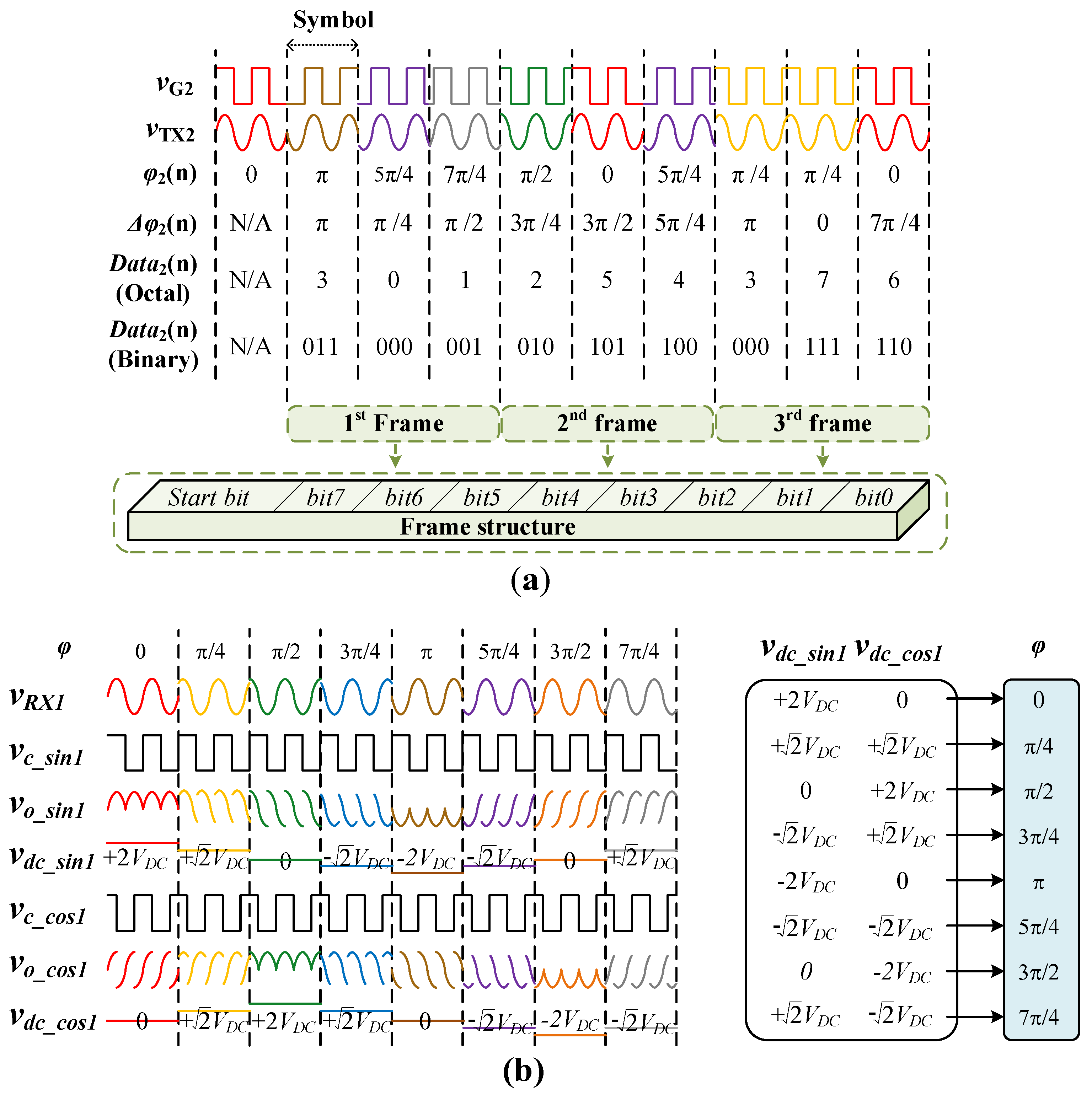
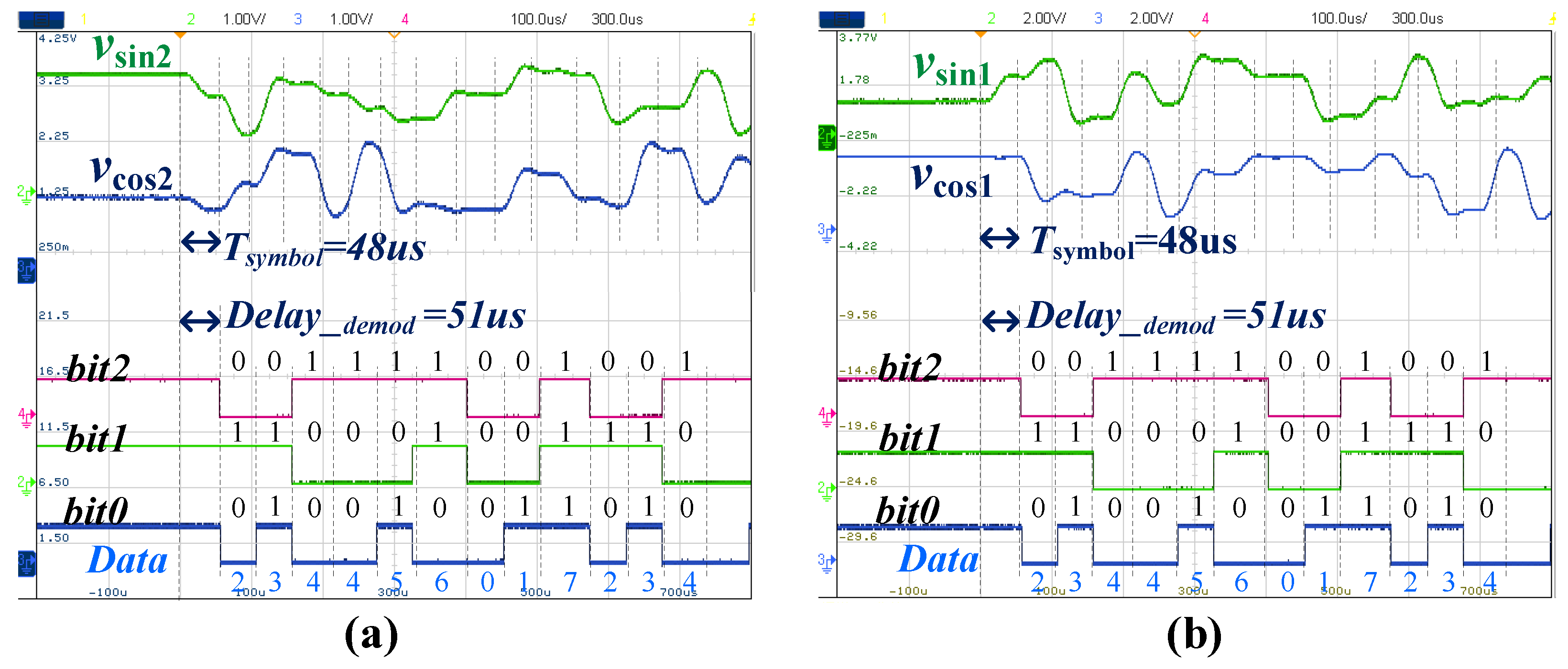
3.2. Data Modulating and Demodulating

In the proposed system, the data are modulated on a high-frequency square-wave carrier using octal differential phase shift keying (8DPSK). As shown in Figure 2, the modulated signal is then used as the drive signal for a class-E inverter, which transmits the data signal to the transceiver transformers. Compared with the traditional class-A, class-B, class-C, and class-D power amplifiers (PAs), the class-E PAs have the advantages of ultra-small static power losses and high efficiency under high-frequency operations. The frequency of the MOSFET STX2′s driving signal is fd2, i.e., the backward data transfer frequency. In PSK modulation, the data are the phase difference ∆φ2 of two adjacent symbols. Thus, the transmitting signal that is acting on LTX2 can be equivalent to a voltage source vTX2 and expressed as follows:
v T X 2 ( t ) = A 2 sin ( 2 π f d 2 t + φ 2 ( n ) )   φ 2 ( n ) { 0 , π 4 , π 2 , 3 π 4 , π , 5 π 4 , 3 π 2 , 7 π 4 } ,
where n is a sequence number of symbols. Similarly, the forward transmitting signal can be regarded as a data voltage source vTX1. Each phase difference of vTX2/vTX1 represents one octal data point or three bits, as shown in Figure 4a.
For practical applications, each byte corresponds to three symbols, including one start bit and eight data bits, where the start bit is set to zero. Thus, each byte frame transmission always starts with a phase change and ends when three symbols are transmitted. Following the transmission of the signal through the channel, the received voltage vRX1 can be expressed as follows:
v R X 1 ( t ) = K 21 A 2 sin ( 2 π f d 2 t + φ 2 ( n ) + φ 21 ) ,
where K21 and φ21 are the gain and the phase shift of the backward data transmission channel, respectively. After turning the received voltage vRX1 into a pair of differential data signals, i.e., vRX11+ and vRX11−, the following Butterworth high-pass filter is used to eliminate the power carrier fundamental component and low-order harmonics. Subsequently, the signals pass through the amplifier with an appropriate amplification factor and an analog switch-based coherent demodulation circuit.
The control signals of the analog switches can be represented by a pair of square-wave signals with a frequency of fd2 and an amplitude of 1, i.e., vcsin1 and vccos1. They can be expressed as follows:
{ v c sin 1 = 4 π k = 1 sin [ ( 2 k 1 ) ω d 2 t ] 2 k 1 v c cos 1 = 4 π k = 1 ( 1 ) k 1 cos [ ( 2 k 1 ) ω d 2 t ] 2 k 1 .
After passing the analog switches, the output signals vosin1 and vocos1 are composed of a DC signal and signals with frequencies of 2kfd2. After passing through the low-pass filter, the output voltages vdcsin1 and vdccos1 can be expressed as follows:
{ v d c sin 1 ( n ) = K R X 1 K 21 A 2 π cos ( φ 2 ( n ) + φ 21 ) v d c cos 1 ( n ) = K R X 1 K 21 A 2 π sin ( φ 2 ( n ) + φ 21 ) .
where KRX1 is the gain of the high-pass filter and amplifier. According to (12), it can be concluded that Vdc in Figure 4b satisfies the expression:
V d c = K R X 1 K 21 A 2 2 π .

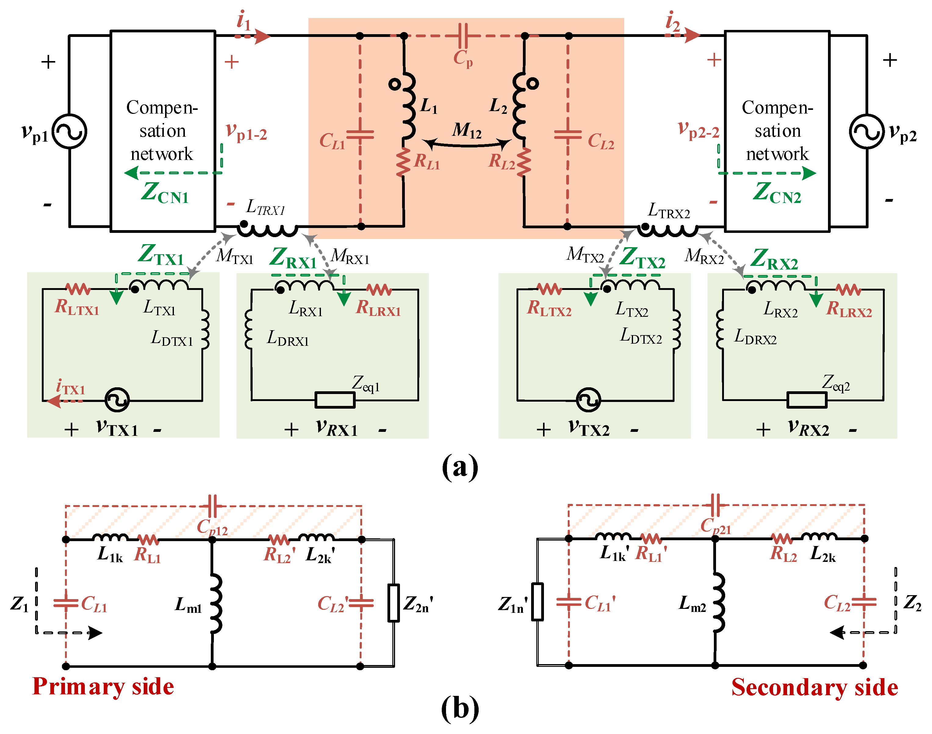
4. Communication Channel Modeling

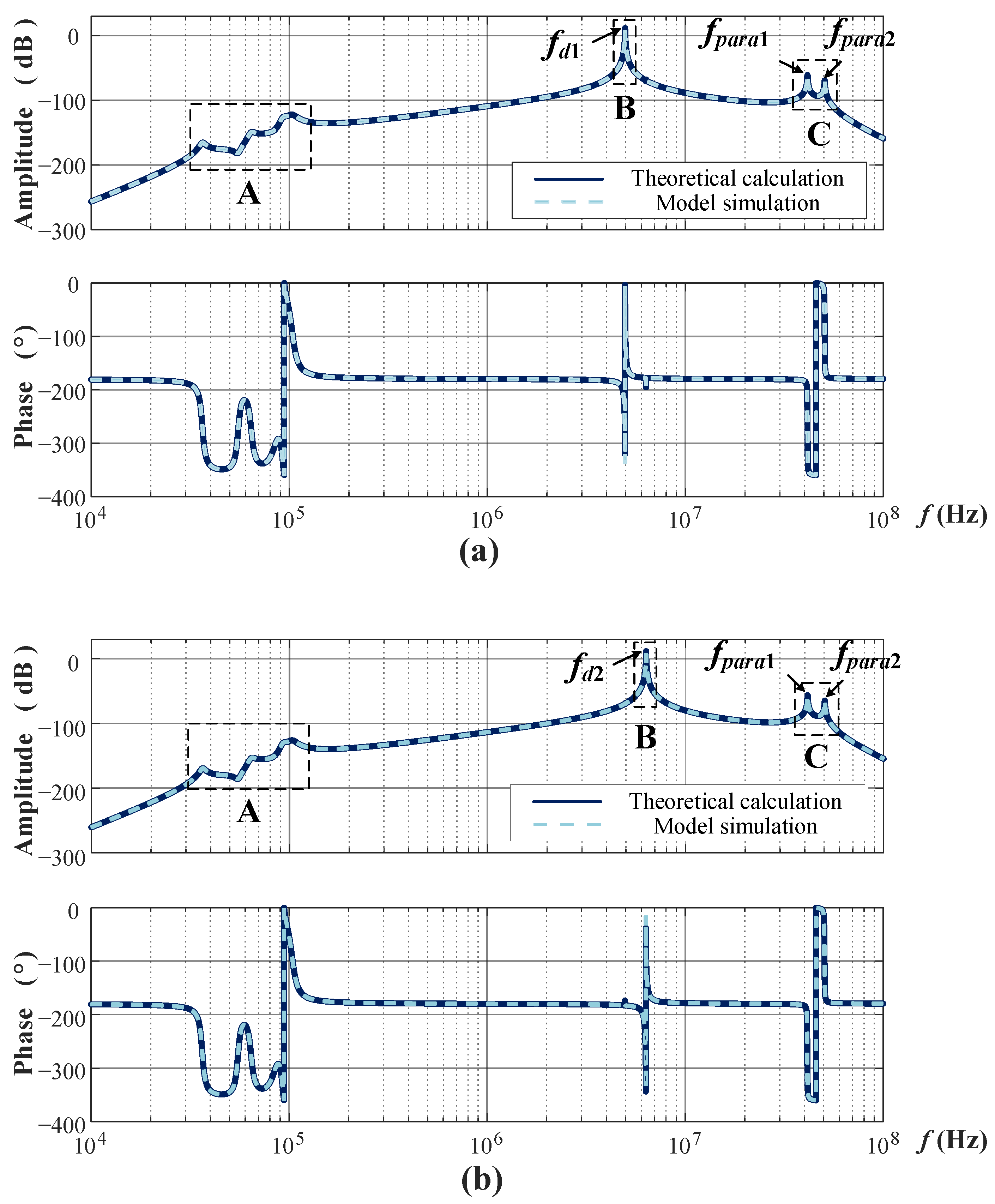
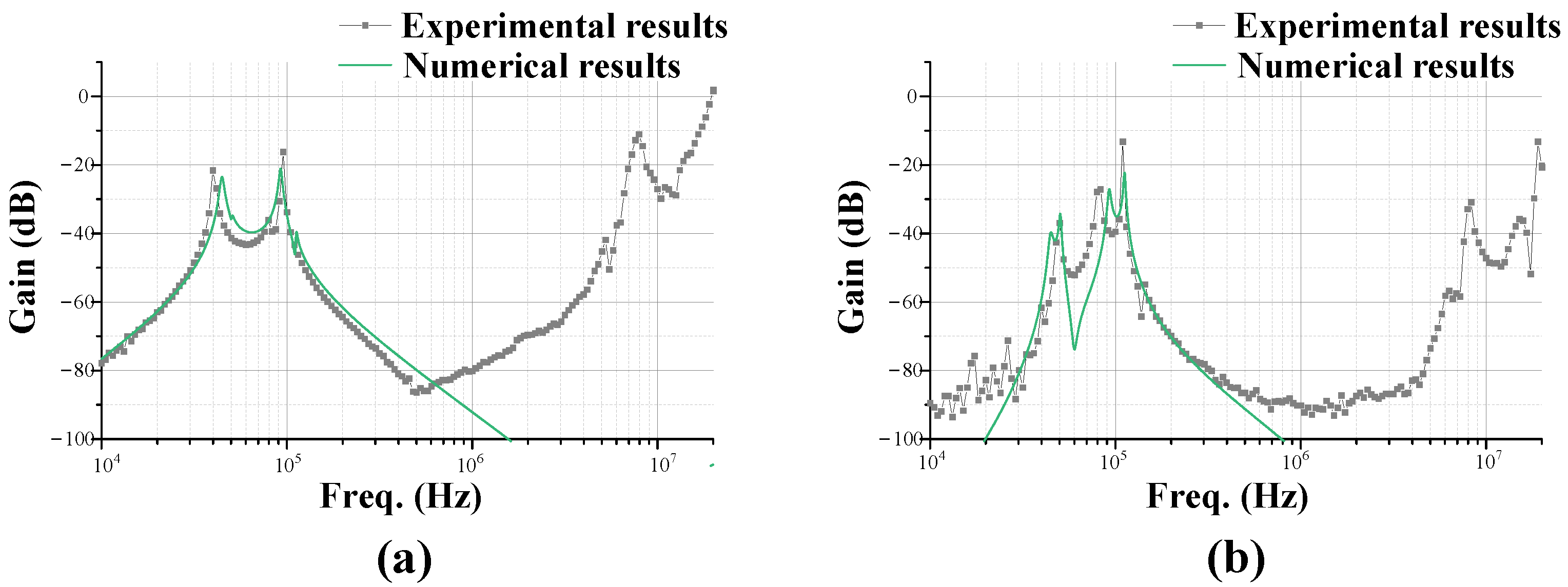
4.1. Data Transfer Gain

The circuit diagrams of the communication channel are given in Figure 5. The circuit parasitic parameters should be taken into consideration when analyzing the communication channel model. For clarity, parasitic parameters in Figure 5 are marked in red. The distribution capacitance between the primary and secondary sides of the transformer, as well as the distribution capacitances on the primary and secondary sides, are taken into consideration in the communication channel model.
The input impedances of the primary and secondary side data transmitter and receiver are as follows:
{ Z R X 1 ( ω ) = j ω ( L R X 1 + L L D R X 1 ) + R L R X 1 + Z e q 1 Z T X 1 ( ω ) = R L T X 1 + j ω ( L T X 1 + L D T X 1 ) Z R X 2 ( ω ) = j ω ( L R X 2 + L L D R X 2 ) + R L R X 2 + Z e q 2 Z T X 2 ( ω ) = R L T X 2 + j ω ( L T X 2 + L D T X 2 ) .
The equivalent circuits referred to on the primary and secondary sides of the power transformer are derived, as shown in Figure 5b. The apostrophe symbols indicate the variables of the secondary side referred to the primary side. The equivalent impedance Z2n on the secondary side of the power transformer can be expressed as follows:
Z 2 n ( ω ) = L 1 L 2 ( ω 2 M R X 2 2 Z R X 2 ( ω ) + ω 2 M T X 2 2 Z T X 2 ( ω ) + j ω L T R X 2 + Z C N 2 ( ω ) ) ,
where ZCN2 is the impedance of the secondary compensation network when vp2 is shorted. As shown in Figure 6, the delta (∆)-connected impedance in the circuit is equivalently transformed into a star (Y)-connected impedance. The ∆-shaped network marked with a red box in Figure 6a can be converted into a Y-shaped network composed of Zy1, Zy2, and Zy3 in Figure 6b. Zy1, Zy2, and Zy3 can be expressed as follows:
{ Z y 1 ( ω ) = L 1 L 2 ( R L 2 + j ω L 2 k ) ( R L 1 + j ω L 1 k ) L 1 L 2 ( R L 2 + j ω L 2 k ) + R L 1 + j ω L 1 k + 1 j ω C p 12 Z y 2 ( ω ) = 1 j ω C p 12 ( R L 1 + j ω L 1 k ) L 1 L 2 ( R L 2 + j ω L 2 k ) + R L 1 + j ω L 1 k + 1 j ω C p 12 Z y 3 ( ω ) = L 1 j ω C p 12 L 2 ( R L 2 + j ω L 2 k ) L 1 L 2 ( R L 2 + j ω L 2 k ) + R L 1 + j ω L 1 k + 1 j ω C p 12 ,
The input impedance of the primary side is Z1, and its value could be obtained as follows:
Z 1 ( ω ) = Z y 2 ( ω ) + ( Z y 3 ( ω ) + Z 2 n ( ω ) ) ( Z y 1 ( ω ) + j ω L m 1 ) .
Then, the total input impedance ZTX1f, viewed from the primary data transmitter side, can be expressed as follows:
Z T X 1 f ( ω ) = ω 2 M T X 1 2 Z C N 1 ( ω ) + Z 1 ( ω ) | | 1 j ω C L 1 + j ω L T R X 1 + ω 2 M R X 1 2 Z R X 1 ( ω ) + j ω ( L T X 1 + L D T X 1 ) + R L T X 1 .
The transfer function of the forward communication channel Gf(ω) can be obtained, which can be expressed as follows:
G f ( ω ) = v R X 2 v T X 1 = L 1 L 2 M R X 2 M T X 1 C L 1 C L 2 Z R X 2 ( ω ) Z 1 ( ω ) Z T X 1 f ( ω ) ( Z y 1 ( ω ) + j ω L m 1 ) Z e q 2 ( ω ) ( Z 1 ( ω ) + 1 j ω C L 1 ) ( Z C N 2 ( ω ) + L 2 L 1 Z 2 n ( ω ) ) ( Z y 1 ( ω ) + Z y 3 ( ω ) + Z 2 n ( ω ) + j ω L m 1 ) .
The transfer function of the backward communication channel Gb(ω) can be derived similarly, as follows:
G b ( ω ) = v R X 1 v T X 2 = L 2 L 1 M R X 1 M T X 2 C L 1 C L 2 Z R X 1 ( ω ) Z 2 ( ω ) Z T X 2 f ( ω ) ( Z y 1 ( ω ) + j ω L m 2 ) Z e q 1 ( ω ) ( Z 2 ( ω ) + 1 j ω C L 2 ) ( Z C N 1 ( ω ) + L 1 L 2 Z 1 n ( ω ) ) ( Z y 1 ( ω ) + Z y 2 ( ω ) + Z 1 n ( ω ) + j ω L m 2 ) .
As shown in Figure 7, the parasitic parameters of the component parts are substituted into (19) and (20) for calculation, and PSpice is used to construct the channel circuit model in order to verify the formula. It is clear that the amplitude-frequency characteristic curve can be separated into three characteristic regions. Electrical and parasitic parameters in the power circuit are what cause Regions A and C, respectively. Region B represents a band-pass communication channel. The gain of the communication channel at the data carrier’s frequency is unrelated to the topology of the power circuit when the impedances ZCN1 and ZCN2 are regarded as zero.

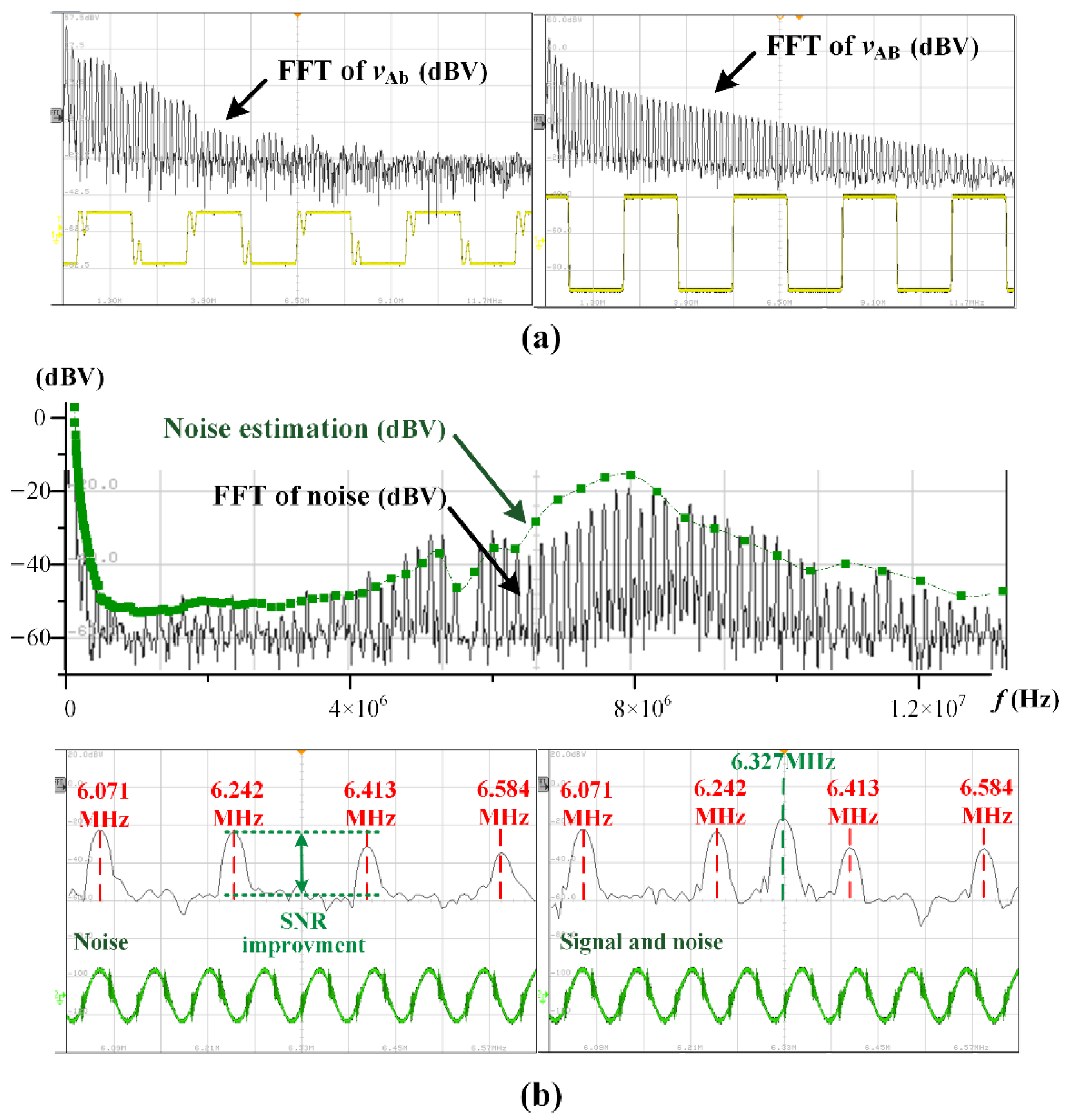
4.2. Interference Analysis

Interference from power transmission is the primary concern of an SWPDT system, limiting its communication performance. Conventionally, the closest odd harmonic among all power harmonics is regarded as the system’s primary interference source [5,12,15], which is calculated as follows:
v N o i s e = v p 1 ( m ω p ) G v p 1 t o v d ( m ω p ) + v p 2 ( m ω p ) G v p 2 t o v d ( m ω p ) .
where Gvp1tovd and Gvp2tovd are the power interference gains from the primary and secondary power noise sources vp1 and vp2 on the received signals, respectively, and m is the order of power harmonics, which can be obtained as follows:
m = f o d d ( ω d ω p ) .
The transfer function of power interference received on the primary side data extractor is calculated as follows:
{ G v p 1 to v d 1 ( ω ) = j ω λ 1 ( ω ) M R X 2 Z e q 1 ( ω ) Z R X 1 ( ω ) ( Z 1 ( ω ) | | 1 j ω C L 1 + j ω L T R X 1 + ω 2 M R X 1 2 Z R X 1 ( ω ) + ω 2 M T X 1 2 Z T X 1 ( ω ) ) G v p 2 to v d 1 ( ω ) = L 2 L 1 j λ 2 ( ω ) ω M R X 1 Z e q 1 ( ω ) ω 2 C L 1 C L 2 ( Z y 1 ( ω ) + j ω L m 2 ) Z R X 1 ( ω ) ( Z 2 ( ω ) | | 1 j ω C L 2 + j ω L T R X 2 + ω 2 M R X 2 2 Z R X 2 ( ω ) + ω 2 M T X 2 2 Z T X 2 ( ω ) ) d e n . G b ( ω ) .
where λ1 and λ2 are the input–output voltage ratios of the primary and secondary compensation networks, respectively, and den.Gb(ω) represents the denominator of the transfer function obtained in (20). The transfer function of power interference received on the secondary side data extractor is calculated as follows:
{ G v p 2 to v d 2 ( ω ) = j ω λ 2 ( ω ) M R X 1 Z e q 2 ( ω ) Z R X 2 ( ω ) ( Z 2 ( ω ) | | 1 j ω C L 2 + j ω L T R X 2 + ω 2 M R X 2 2 Z R X 2 ( ω ) + ω 2 M T X 2 2 Z T X 2 ( ω ) ) G v p 1 to v d 2 ( ω ) = L 1 L 2 j λ 1 ( ω ) ω M R X 2 Z e q 2 ( ω ) ω 2 C L 1 C L 2 ( Z y 1 ( ω ) + j ω L m 1 ) Z R X 2 ( ω ) ( Z 1 ( ω ) | | 1 j ω C L 1 + j ω L T R X 1 + ω 2 M R X 1 2 Z R X 1 ( ω ) + ω 2 M T X 1 2 Z T X 1 ( ω ) ) d e n . G f ( ω ) .
where den.Gf(ω) represents the denominator of the transfer function obtained in (19).
Based on OF-SWPDT and bandwidth guard intervals, the interference of the power carrier’s fundamental component and its high-order harmonics, as well as the interference between data carriers, are categorically referred to as adjacent channel interference. Compared to conventional SWPDT, the interference in the OF-SWPDT system is significantly reduced, as demonstrated by the experiments in Section 5.

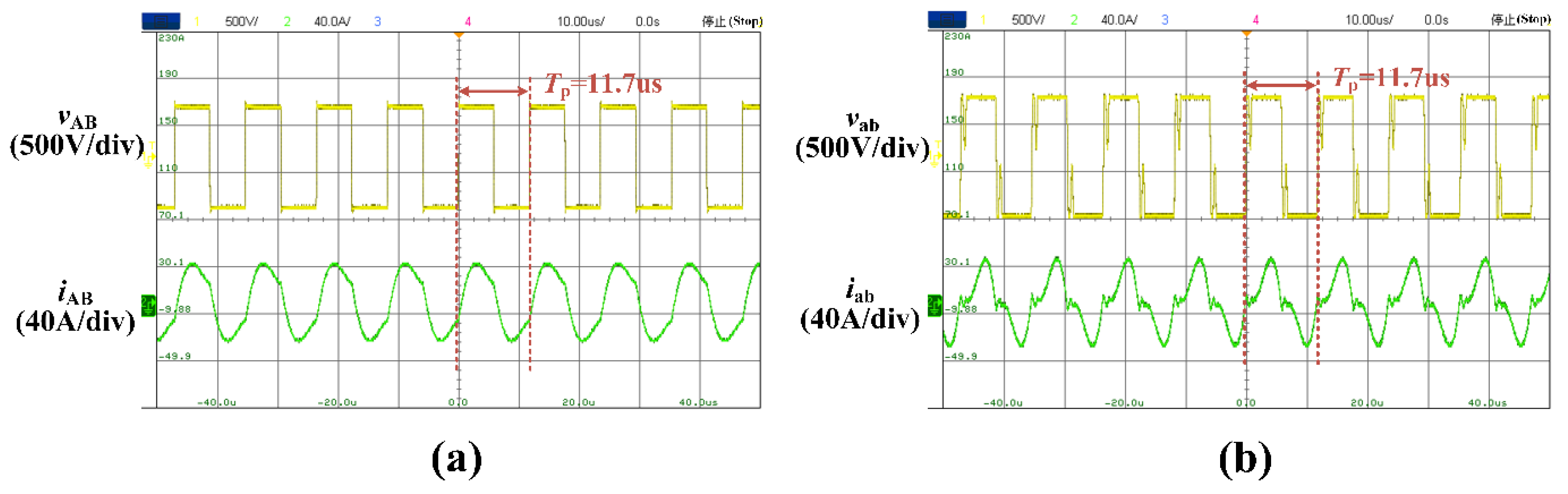
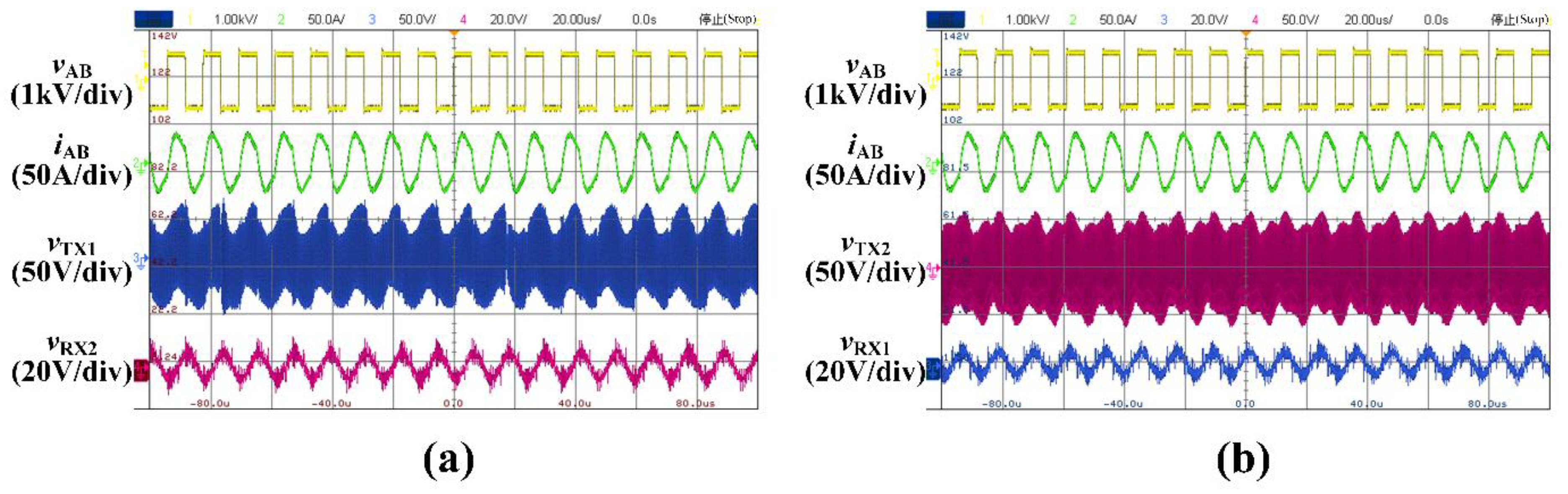
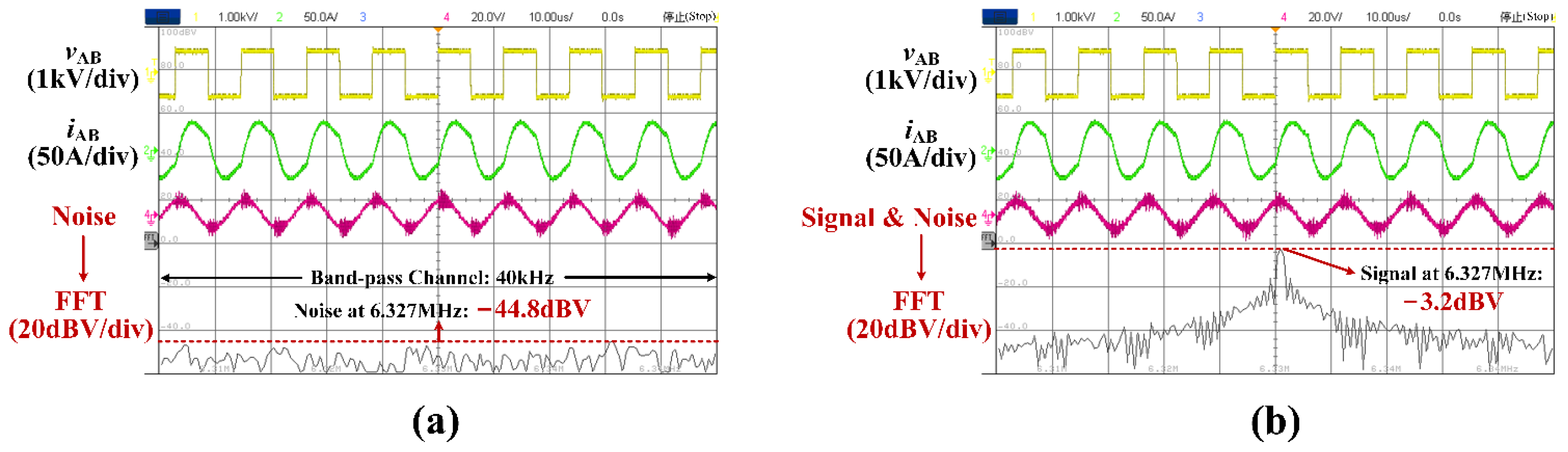
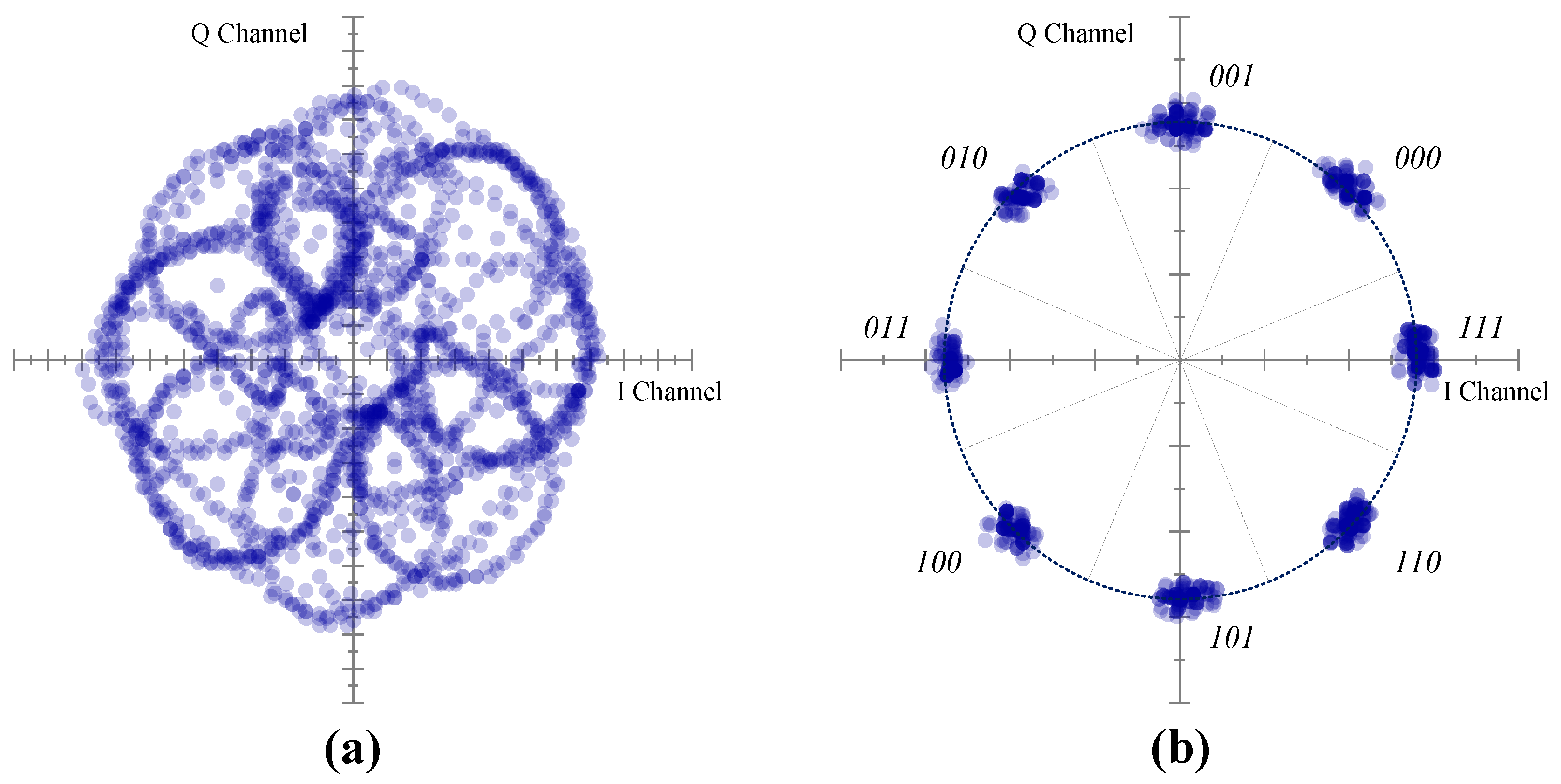
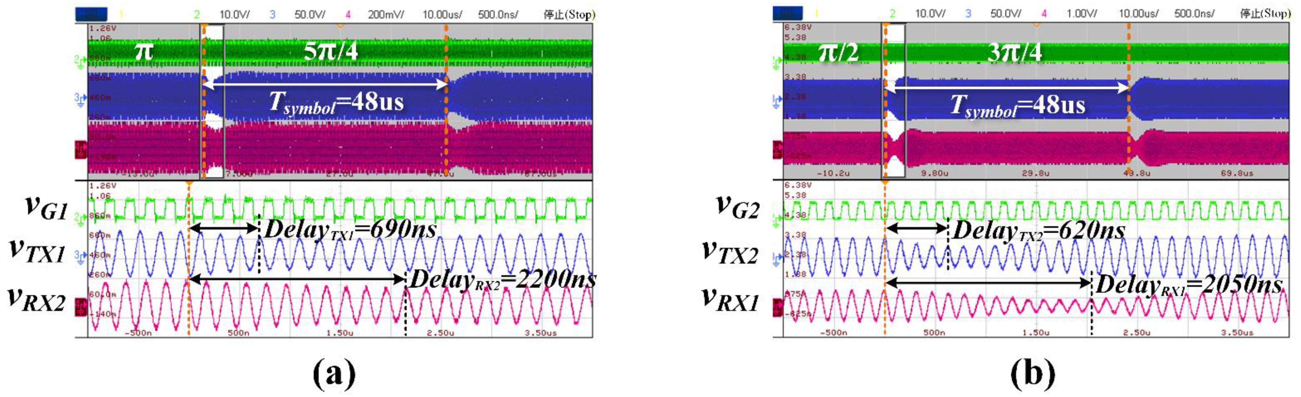
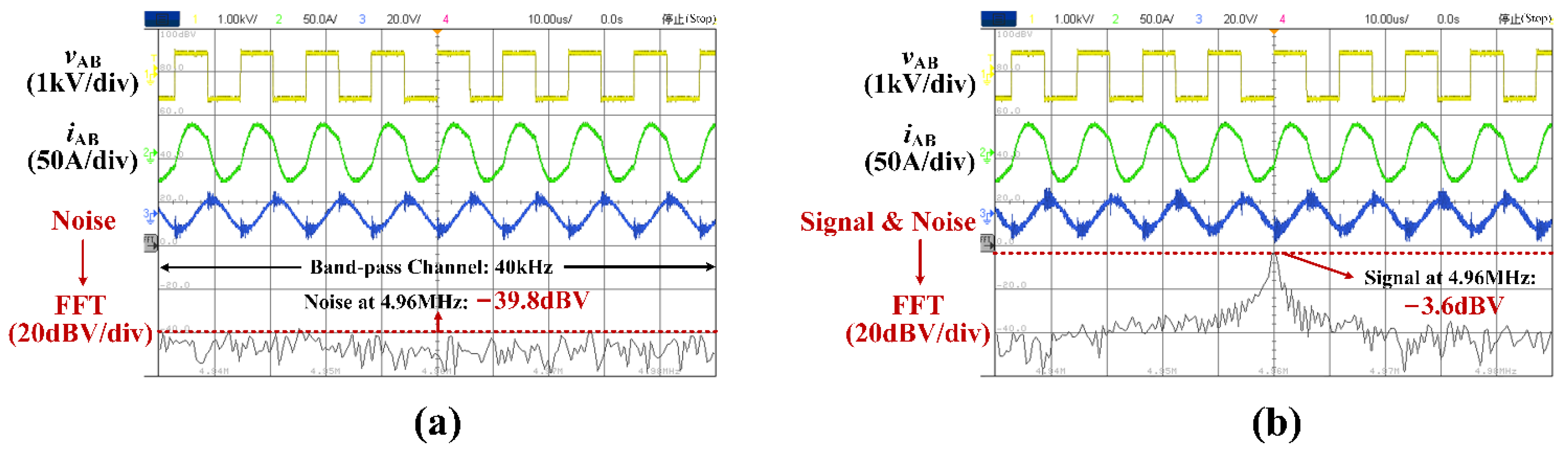
5. Experimental Verification

To verify the effectiveness of the proposed OF-SWPDT technique, a prototype WPT system operating at 85.5 kHz with 11 kW is built, as shown in Figure 8, with the parameters listed in Table 1. As shown in Figure 8a, the double-sided LCC compensation network is used. S1~S4 are four MOSFETs in the primary side power inverter. D1~D4 are the diodes in the secondary side rectifier.
Full-duplex communication is achieved between the primary side and the secondary side during high-power wireless charging. The forward and backward data carrier frequencies are selected to be 4.959 MHz and 6.327 MHz, respectively, to meet the orthogonality constraint. The symbol rate is chosen to be 21.38 kBaud, and the communication rate is 64.125 kbps.
The power inverter output voltage and current waveforms are shown in Figure 9a, and the power rectifier input voltage and current waveforms are shown in Figure 9b. The voltage and current waveforms of power transfer have a period of 11.7 μs, corresponding to the switching frequency of 85.5 kHz. Due to the inductive impedance of the primary compensation network, the output current of the inverter lags slightly behind the voltage.
The waveforms of 11 kW power transfer and full-duplex data transfer under 11 kW power transfer are shown in Figure 10. The power inverter output voltage vAB and current iAB are shown in CH1 and CH2. The data transmitting voltage vLTX1/2 and receiving voltage vRX2/1 are shown in CH3 and CH4. Due to the high power transfer level, the fundamental component of the power carrier (85.5 kHz) in the received signals vRX1 and vRX2 has a high amplitude. However, based on the OF-SWPDT technique proposed in this paper, the noises are classified as adjacent channel interference, which can be effectively filtered out.
The modulation waveforms are shown in Figure 11, wherein vG1 and vG2 are the gate-driving waveforms of the MOSFET in a class-E inverter. After passing through the data demodulation circuit, the fundamental and higher-harmonic components of the power carrier and interference caused by the reverse data carrier all travel to a frequency range far higher than the low-pass filter’s cutoff frequency, where they could be entirely filtered. As shown in Figure 12, only the communication baseband signal is kept after the demodulation and filtering circuits. Figure 12 depicts the forward and backward demodulation waveforms, where vsin1/2 and vcos1/2 are the low-pass filtered outputs of the received signal multiplied by 4.959/6.327 MHz sine and cosine waveforms, and bit2, bit1, and bit0 represent the received octal data. It can be seen that the delay time of demodulation is 51 μs.
The following experiments are conducted to demonstrate how the proposed OF-SWPDT method enhances SNR.
First, the transfer gain Gp2d from the power coil to the data carrier receiver is measured by a frequency response analysis tool based on a Keysight DSOX 3024T oscilloscope. The measured result is contrasted with the numerical calculation in Figure 13. It can be observed that the numerical calculation curve is almost matched with the experimental results in the low-frequency range, which verifies the correctness of the circuit model.
Then, a Fourier analysis is performed on the primary side output voltage of the inverter vab and the secondary side input voltage of the rectifier vAB, which are shown in Figure 14a. Furthermore, the noise on the receiver is estimated by multiplying the fast Fourier transform (FFT) results of the input–output voltage by the measured transfer gain Gp2d, which is shown in Figure 14b, and comparing it to the spectrum measured directly on the receiver. It can be proven that the noise primarily originates from the power sources on the primary and secondary sides. The measured spectrum is zoomed in near the frequency fd2. It is observed that the noise amplitude at the frequencies 6.242 MHz and 6.413 MHz (closest odd harmonics) is higher than the noise amplitude at the carrier frequency 6.327 MHz. The results indicate that the orthogonal frequency selection method and bandwidth limitation rules have improved SNR.
The SNR at the primary and secondary side receivers was further measured in the experiments that followed.
Under an 11 kW power transfer, the amplitude of noise and signal in the backward channel was measured, as shown in Figure 15. The power inverter output voltage vAB and current iAB are shown in CH1 and CH2. The receiving voltage on the primary side data receiver and the FFT results are shown in CH3 and CH4. The measured spectrum has a center frequency of around 6.327 MHz and a range of 40 kHz, which corresponds to the bandwidth of the backward channel. The noise in the backward channel in the absence of data transfer is shown in Figure 15a, which is approximately −44.8 dBV. Figure 15b shows the signal intensity, which is approximately −3.2 dBV.
Similarly, the amplitude of noise and signal in the forward channel under an 11 kW power transfer was measured, as shown in Figure 16. The power inverter output voltage vAB and current iAB are shown in CH1 and CH2. The receiving voltage on the secondary side data receiver and the FFT results are shown in CH3 and CH4. The measured spectrum has a center frequency of around 4.96 MHz and a range of 40 kHz, which corresponds to the bandwidth of the forward channel. The noise in the forward channel in the absence of data transfer is shown in Figure 16a, which is approximately −39.8 dBV. Figure 16b shows the signal intensity, which is approximately −3.6 dBV.
Table 2 displays the signal-to-noise ratio of forward and backward data transfer under an 11 kW power transfer, which can be calculated using the measurement results mentioned above. According to Table 2, SNR is 36.2 dB for forward data transfer and 41.6 dB for backward data transfer.
Conventionally, the constellation diagram can indicate the quality of a communication system. Figure 17a depicts a constellation whose carrier frequency is assigned to the frequency of an odd power harmonic, whereas Figure 17b depicts a constellation with an orthogonal carrier frequency. Clearly, the OF-SWPDT is better suited for high-power systems than conventional SWPDT.
Finally, the performances of the proposed method in comparison with the previous literature are summarized in Table 3. The proposed SWPT system provides 11 kW of output power at a full-duplex communication rate of 64.125 kbps. Clearly, the proposed OF-SWPDT method can operate at higher power levels than previous methods. In addition, it consumes little power for data transmission, which reduces the impact of data transmission on power transmission.

6. Conclusions

This paper proposes an OF-SWPDT technique to mitigate communication interference caused by power transmission in a high-power wireless charging system. To minimize cross-interference, the frequency of the data carrier is chosen to be an even multiple of the frequency of the power carrier. Further, the adoption of bandwidth restriction regulations prevents interference of power harmonics with the data spectrum.
In addition, DPSK modulation with strong anti-interference is adopted, and octal coding is adopted to reduce the occupied bandwidth. In the circuit structure design, decoupling transformers are proposed to decouple the signal injection inductance and signal extraction inductance sharing the magnetic loop. During data demodulation, the adjacent-channel interference of the power carrier is eliminated through signal processing. However, this technique is only applicable for WPT systems with a fixed frequency of power transfer and not for those with a variable frequency.

Author Contributions

Conceptualization, C.L., Y.Z. and J.W.; data curation, C.L.; software, C.L.; validation, C.L. and Y.Z.; formal analysis, C.L.; investigation, C.L. and Y.Z.; writing—original draft preparation, C.L.; writing—review and editing, C.L., H.C. and J.W.; visualization, H.C.; supervision, J.W. and X.H.; funding acquisition, X.H. All authors have read and agreed to the published version of the manuscript.

Funding

This research was funded by the National Natural Science Foundation of China, under Grant 52350003.

Data Availability Statement

The original contributions presented in the study are included in the article, further inquiries can be directed to the corresponding authors.

Conflicts of Interest

The authors declare no conflicts of interest.

References

  1. Jeong, S.; Jang, Y.J.; Kum, D. Economic analysis of the dynamic charging electric vehicle. IEEE Trans. Power Electron. 2015, 30, 6368–6377. [Google Scholar] [CrossRef]
  2. Covic, G.A.; Boys, J.T. Modern trends in inductive power transfer for transportation applications. IEEE J. Emerg. Sel. Top. Power Electron. 2013, 1, 28–41. [Google Scholar] [CrossRef]
  3. Chen, H.; Cheng, Z.; Qian, Z.; Wu, J.; He, X. Application of SWPDT in the Feedback Control of Wireless EV Charging. In Proceedings of the 2020 IEEE Energy Conversion Congress and Exposition (ECCE), Detroit, MI, USA, 11–15 October 2020. [Google Scholar]
  4. Li, C.; Huang, H.; Li, L. State monitoring system based on wireless charging. In Proceedings of the 2019 IEEE International Conference on Energy Internet (ICEI), Nanjing, China, 27–31 May 2019. [Google Scholar]
  5. Yao, Y.; Tang, C.; Gao, S.; Wang, Y.; Alonso, J.M.; Madawala, U.K.; Xu, D. Analysis and design of a simultaneous wireless power and data transfer system featuring high data rate and signal-to-noise ratio. IEEE Trans. Ind. Electron. 2021, 68, 10761–10771. [Google Scholar] [CrossRef]
  6. Chen, H.; Liu, C.; Zhang, Y.; Liu, S.; Wu, J.; He, X. Metal Object and Vehicle Position Detections Integrated With Near-Field Communication for Wireless EV Charging. IEEE Trans. Veh. Technol. 2022, 71, 7134–7146. [Google Scholar] [CrossRef]
  7. Yao, Y.; Sun, P.; Liu, X.; Wang, Y.; Xu, D. Simultaneous wireless power and data transfer: A comprehensive review. IEEE Trans. Power Electron. 2022, 37, 3650–3667. [Google Scholar] [CrossRef]
  8. Hoeher, P.A. FSK-based simultaneous wireless information and power transfer in inductively coupled resonant circuits exploiting frequency splitting. IEEE Access 2019, 7, 40183–40194. [Google Scholar] [CrossRef]
  9. Kim, J.G.; Wei, G.; Kim, M.H.; Ryo, H.S.; Zhu, C. A wireless power and information simultaneous transfer technology based on 2FSK modulation using the dual bands of series–parallel combined resonant circuit. IEEE Trans. Power Electron. 2019, 34, 2956–2965. [Google Scholar] [CrossRef]
  10. Qian, Z.; Yan, R.; Wu, J.; He, X. Full-duplex high-speed simultaneous communication technology for wireless EV charging. IEEE Trans. Power Electron. 2019, 34, 9369–9373. [Google Scholar] [CrossRef]
  11. Wang, P.; Sun, Y.; Feng, T.; Fan, Y.; Feng, Y. Simultaneous wireless power and data transfer system with full-duplex mode based on double-side LCCL and dual-notch filter. IEEE J. Emerg. Sel. Top. Power Electron. 2021, 10, 3140–3151. [Google Scholar] [CrossRef]
  12. Jing, Y.; Feng, W.; Qiao, K.; Yang, L.; Wang, S.; Lu, L. Simultaneous Wireless Power and Data Transfer System With Full-Duplex Mode Based on LCC/CLC Resonant Network. IEEE Trans. Power Electron. 2023, 38, 5549–5560. [Google Scholar] [CrossRef]
  13. Wang, K.; Sanders, S. Contactless USB—A capacitive power and bidirectional data transfer system. In Proceedings of the 2014 IEEE Applied Power Electronics Conference and Exposition-APEC, Fort Worth, TX, USA, 16–20 March 2014. [Google Scholar]
  14. Yao, Y.; Cheng, H.; Wang, Y.; Mai, J.; Lu, K.; Xu, D. An FDM-based simultaneous wireless power and data transfer system functioning with high-rate full-duplex communication. IEEE Trans. Ind. Inform. 2020, 16, 6370–6381. [Google Scholar] [CrossRef]
  15. Wang, P.; Sun, Y.; Feng, Y.; Feng, T.; Fan, Y.; Li, X. An improvement of SNR for simultaneous wireless power and data transfer system with full-duplex communication mode. IEEE Trans. Power Electron. 2022, 37, 2413–2424. [Google Scholar]
  16. Ji, L.; Wang, L.; Liao, C.; Li, S. Simultaneous wireless power and bidirectional information transmission with a single-coil, dual-resonant structure. IEEE Trans. Ind. Electron. 2019, 66, 4013–4022. [Google Scholar] [CrossRef]
  17. Yao, G.; Guo, W.; Xiaoxiao, H. Study on Wireless Power and Information Synchronous Transfer Based on Dual Resonant Coupling Circuits. Trans. China Electrotech. Soc. 2015, 30, 18–25. [Google Scholar]
  18. Fan, Y.; Sun, Y.; Dai, X.; Zuo, Z.; You, A. Simultaneous wireless power transfer and full-duplex communication with a single coupling interface. IEEE Trans. Power Electron. 2021, 36, 6313–6322. [Google Scholar] [CrossRef]
  19. Wu, J.; Zhao, C.; Lin, Z.; Du, J.; Hu, Y.; He, X. Wireless power and data transfer via a common inductive link using frequency division multiplexing. IEEE Trans. Ind. Electron. 2015, 62, 7810–7820. [Google Scholar] [CrossRef]
  20. Sun, Y.; Yan, P.X.; Wang, Z.H.; Luan, Y.Y. The parallel transmission of power and data with the shared channel for an inductive power transfer system. IEEE Trans. Power Electron. 2016, 31, 5495–5502. [Google Scholar] [CrossRef]
  21. Wang, G.; Wang, P.; Tang, Y.; Liu, W. Analysis of dual band power and data telemetry for biomedical implants. IEEE Trans. Biomed. Circuits Syst. 2012, 6, 208–215. [Google Scholar] [CrossRef] [PubMed]
  22. Bieler, T.; Perrottet, M.; Nguyen, V.; Perriard, Y. Contactless power and information transmission. IEEE Trans. Ind. Appl. 2002, 38, 1266–1272. [Google Scholar] [CrossRef]
  23. Li, X.; Hu, J.; Li, Y.; Wang, H.; Liu, M.; Deng, P. A decoupled power and data-parallel transmission method with four-quadrant misalignment tolerance for wireless power transfer systems. IEEE Trans. Power Electron. 2019, 34, 11531–11535. [Google Scholar] [CrossRef]
  24. Fan, Y.; Hu, H.; Sun, Y.; Hu, H.; Wu, S. Simultaneous Wireless Power and Coil Inductance Insensitive Data Transfer System for Rotary Structures. IEEE Trans. Power Electron. 2024, 39, 6526–6536. [Google Scholar]
Figure 1. Spectra of the OF-SWPDT system when (a) Ts = 1/fp; (b) Ts = 4/fp.
Energies 17 01851 g001
Figure 2. Diagram of the proposed OF-SWPDT system.
Energies 17 01851 g002
Figure 3. The equivalent decoupling circuit of the plug-and-play toroidal transformer.
Energies 17 01851 g003
Figure 4. Modulation and demodulation. (a) Waveforms and frame structure of modulation. (b) Waveforms and mapping relationships of the demodulated results.
Energies 17 01851 g004
Figure 5. Circuit diagrams: (a) circuit considering transformer distribution parameters; (b) equivalent circuit referred to the primary and secondary sides.
Energies 17 01851 g005
Figure 6. Equivalent conversion: (a) Δ-shaped network; (b) Y-shaped network.
Energies 17 01851 g006
Figure 7. Bode diagram of transfer functions: (a) Gf; (b) Gb.
Energies 17 01851 g007
Figure 8. Prototype of the system. (a) SWPDT system. (b) Power coils.
Energies 17 01851 g008
Figure 9. Waveforms of 11 kW power transfer: (a) the power inverter output voltage and current waveforms; (b) the power rectifier input voltage and current waveforms.
Energies 17 01851 g009
Figure 10. Waveforms of power transfer and full-duplex data transfer: (a) Forward data transfer waveforms under 11 kW power transfer. (b) Backward data transfer under 11 kW power transfer.
Energies 17 01851 g010
Figure 11. 8DPSK modulation and data carrier waveforms: (a) forward data transfer; (b) backward data transfer.
Energies 17 01851 g011
Figure 12. Demodulation waveforms of (a) forward data transfer and (b) backward data transfer.
Energies 17 01851 g012
Figure 13. (a) Forward power interference transmission gain. (b) Backward power interference transmission gain.
Energies 17 01851 g013
Figure 14. FFT analysis of (a) power interferences from the primary and secondary sides and (b) noise in the channel under power transfer.
Energies 17 01851 g014
Figure 15. Waveforms of 11 kW power transfer and FFT analysis of (a) noise in the backward channel under 11 kW power transfer and (b) signal in the backward channel under 11 kW power transfer.
Energies 17 01851 g015
Figure 16. Waveforms of 11 kW power transfer and FFT analysis of (a) noise in the forward channel under 11 kW power transfer and (b) signal in the forward channel under 11 kW power transfer.
Energies 17 01851 g016
Figure 17. Constellation (a) without orthogonal frequency selection and (b) with orthogonal frequency selection.
Energies 17 01851 g017
Table 1. Experimental parameters.
SymbolValueDescription
WPT Systemfp85.5 kHzSwitching frequency
P11 kWTransferred power
η91%Power transmission efficiency
L1, L241.7 μH, 38.8 μHInductive coupled coils
M124.94 μHMutual inductance between L1 and L2
RL1, RL20.12 Ω, 0.1 ΩParasitic resistor of L1 and L2
C1, C2126 nF, 157 nFCompensation capacitors
Cf1, Cf2273 nF, 205 nFCompensation capacitors
Lf1, Lf226 μH, 16 μHCompensation inductors
RL43 ΩLoad Resistor
S1~S4IPW65R080CFDPower inverter switches
D1~D4IDW30S120Power rectifier diodes
Communication Systemfd1, fd24.959 MHz, 6.327 MHzFrequency of data carriers
Pd1, Pd21.7 W, 1.4 WPower consumptions of data transmitting
LTX1, LTX22.2 μH, 2.56 μHData-injecting inductors
LRX1, LRX27.28 μH, 6.50 μHData-extracting inductors
Req4.88 kΩData extractor equivalent resistor
Table 2. SNR under 11 kW power transfer.
Signal (dBV)Noise (dBV)SNR (dB)
Forward data transfer (4.96 MHz)−3.6−39.836.2
Backward data transfer (6.327 MHz)−3.2−44.841.6
Table 3. Performance comparison.
ReferenceThis Work[24],
Year 2024
[12],
Year 2023
[15],
Year 2022
[18],
Year 2021
[14],
Year 2020
Transferred power11 kW300 W20 W500 W600 W300 W
Power transmission efficiency91%90.5%80%84%85%90.1%
Maximum data transfer rate64.1 kbps40 kbps250 kbps600 kbps80 kbps500 kbps
Power consumption from data transmission1.7 W, 1.4 W----2 W
Modulation8DPSKASKASKASKASKFSK
SNR36.2 dB--32 dB8.6 dB20 dB
Communication modeFull-duplexFull-duplexFull-duplexFull-duplexFull-duplexFull-duplex
Disclaimer/Publisher’s Note: The statements, opinions and data contained in all publications are solely those of the individual author(s) and contributor(s) and not of MDPI and/or the editor(s). MDPI and/or the editor(s) disclaim responsibility for any injury to people or property resulting from any ideas, methods, instructions or products referred to in the content.

