Article

Second-Order Ripple Current Suppression Based on Virtual Impedance in the Application of Dynamic Voltage Restorer

1
Foshan Power Supply Bureau of Guangdong Power Grid Co., Ltd., Foshan 528000, China
2
School of Automation and Science and Engineering, South China University of Technology, Guangzhou 510006, China
*
Author to whom correspondence should be addressed.
Energies 2025, 18(8), 1896; https://doi.org/10.3390/en18081896
Submission received: 10 March 2025 / Revised: 31 March 2025 / Accepted: 6 April 2025 / Published: 8 April 2025

Abstract

:
In existing two-stage single-phase dynamic voltage restorer (DVR) voltage sag mitigation devices, the output-side power contains a pulsating component at twice the fundamental frequency (2f0), leading to the presence of second-order ripple currents (SRCs) on the DC input side. This, to some extent, affects the reliability of the system and has a significant impact on the lifespan of energy storage devices. In this study, the dual-loop control method of the buck/boost converter is combined with the virtual impedance auxiliary control strategy to suppress SRCs. Compared to existing solutions, this method offers the advantages of being fast, stable, and reliable, while the virtual impedance auxiliary control strategy is flexible and easy to implement. The feasibility and stability of this strategy were verified using a 3 kW DVR prototype. When applying the two virtual impedance methods, the second harmonic content was reduced from 39.64% to 1.74% and 1.78%, respectively. The proposed control strategy demonstrates significant effectiveness in suppressing second harmonic currents.

1. Introduction

With the gradual development of industrial power distribution systems, power quality issues have increasingly garnered attention [1]. Among various power quality problems, such as voltage flicker, sag, and harmonics, voltage sags occur most frequently and are one of the significant causes of reduced stability in electrical equipment [2,3,4]. Voltage sags can lead to the abnormal operation of numerous sensitive devices, resulting in incalculable losses [5]. With its benefits of cost-effectiveness, high efficiency, and rapid response, the dynamic voltage restorer (DVR) stands out as a compelling solution for mitigating voltage sag issues [6,7].
For medium and low power levels, as well as for ease of implementation, a single-phase two-stage scheme is adopted typically. Figure 1 illustrates the system structure of DVR, which consists of energy storage (ES), a front-stage DC-DC converter for stepping up the voltage, a rear-stage DC-AC inverter, and a large-capacity capacitor C b u s to maintain the input voltage of the rear-stage DC-AC inverter. Finally, it is connected to the equipment or sensitive load. During DC-AC conversion, second-order pulsations in AC-side output power are also observed in the DC-side input voltage and current. Typically, the input-side voltage is controlled at a constant value, so the second-order oscillations primarily appear in the input current. Since the energy source usually consists of battery components such as lithium batteries or fuel cells, these second-order ripple currents (SRCs) reflected on the input side can cause various harmful effects. In reference [8], SRCs could induce approximately 22% additional thermal losses, leading to increased temperature in battery packs. Temperature significantly impacts both battery capacity and lifespan. References [9,10] further indicate that a 30 °C temperature rise can reduce lithium-ion battery lifespan by up to 60%. Moreover, high temperatures may trigger safety concerns in lithium-ion batteries, compromising the reliability of both the energy storage system and the DVR device. Therefore, it is essential to effectively suppress SRCs in DVR devices.
In the literature, there are both passive and active methods to suppress SRCs. Passive methods include adding capacitors and inductors to eliminate the SRC components. However, the large size of these components leads to oversized designs and high system costs. A few power decoupling thoughts are proposed for eliminating SRCs in [11,12]. Ordinary electrolytic capacitors are substituted with longer-lasting film capacitors, improving the system’s durability [13]. Additionally, the most direct way to suppress the SRCs is to increase the capacitance of the intermediate DC bus. However, high-capacity electrolytic capacitors have a shorter lifespan, which reduces the service life of devices [14,15].
The second passive method involves applying auxiliary control methods in the front-stage DC-DC converter to suppress the SRCs flowing to the input side. Earlier ripple reduction methods primarily focused on introducing an inductor current feedback loop to create dual-loop control [16]. But this approach reduces the cutoff frequency of the voltage loop, resulting in a significant overshoot on the bus voltage when the load is suddenly changed. To suppress SRCs while maintaining the system’s dynamic performance, the authors of [17,18] introduced notch filters into the voltage feedback path, while the authors of [19] incorporated bandpass filters into the current feedback path. However, both methods introduce significant negative phase shifts, which affect system stability. In [20,21], the virtual impedance method was applied to regulate the input or output impedance at specific frequencies to suppress SRCs. This approach does not require additional components and is easy to implement. In [22,23], the method of paralleling virtual impedance across the bus capacitor was proposed to decrease bus voltage overshoots during variations in the load. In [24], a control scheme with the virtual fractional-order inductance is proposed. In [25], the authors proposed a deadbeat control method to optimize the traditional PI controller. The primary control methods used in the above studies are based on single-output-side bus voltage feedback control. Compared to dual-loop control, this single voltage feedback control exhibits poorer dynamic performance and lower system robustness. In [26], the authors combined droop control, dual-loop control of bus voltage and inductor current, and a notch filter to suppress SRCs. In [27], the authors proposed a simplified model for the front-stage buck/boost converter and employed dual-loop control of bus voltage and inductor current, combined with a digital notch filter to suppress SRCs. This approach reduces control complexity, but the digital notch filter introduces phase delay and is only effective at specific frequencies. Compared to the droop control strategy and digital notch filter proposed in [26,27], the virtual impedance method is simpler to implement, more flexible, and does not require integration with other methods. At the same time, few studies have explicitly proposed combining dual-loop control with the virtual impedance method to suppress SRCs.
In this study, a method for suppressing DC-side SRCs in DVR devices is proposed. Firstly, based on the dual feedback loops (voltage and current) of the front-stage buck/boost converter, the virtual series impedance (VSI) and the virtual parallel impedance (VPI) are introduced to step up the equivalent impedance at 2f0, which effectively suppresses SRCs. The proposed control method takes advantage of the fast, stable, and reliable characteristics of dual closed-loop control, while the virtual impedance-assisted control strategy is flexible and easy to implement. Next, the propagation mechanism of SRCs and the suppression method based on virtual impedance are described. Then, the selection of virtual impedance and the design of key parameters are introduced. Finally, a 3 kW single-phase DVR experimental prototype is built, and the results are discussed.

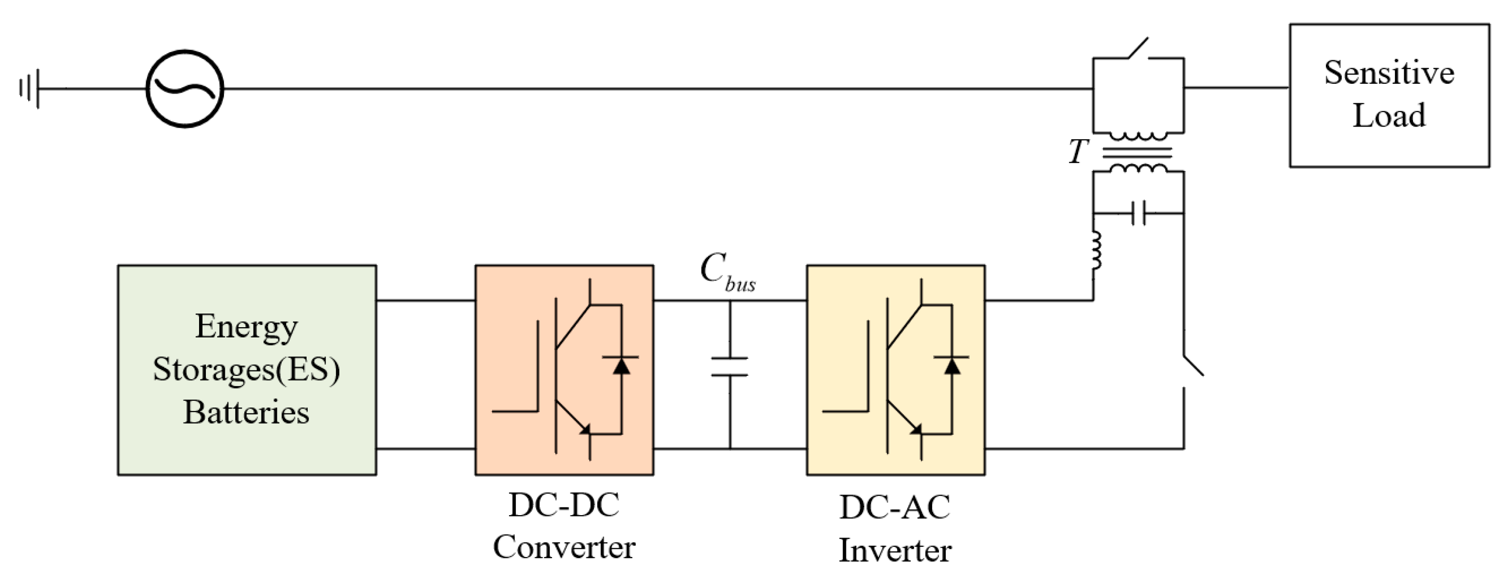
2. SRC Generation Mechanisms and Suppression Methods Based on Virtual Impedances

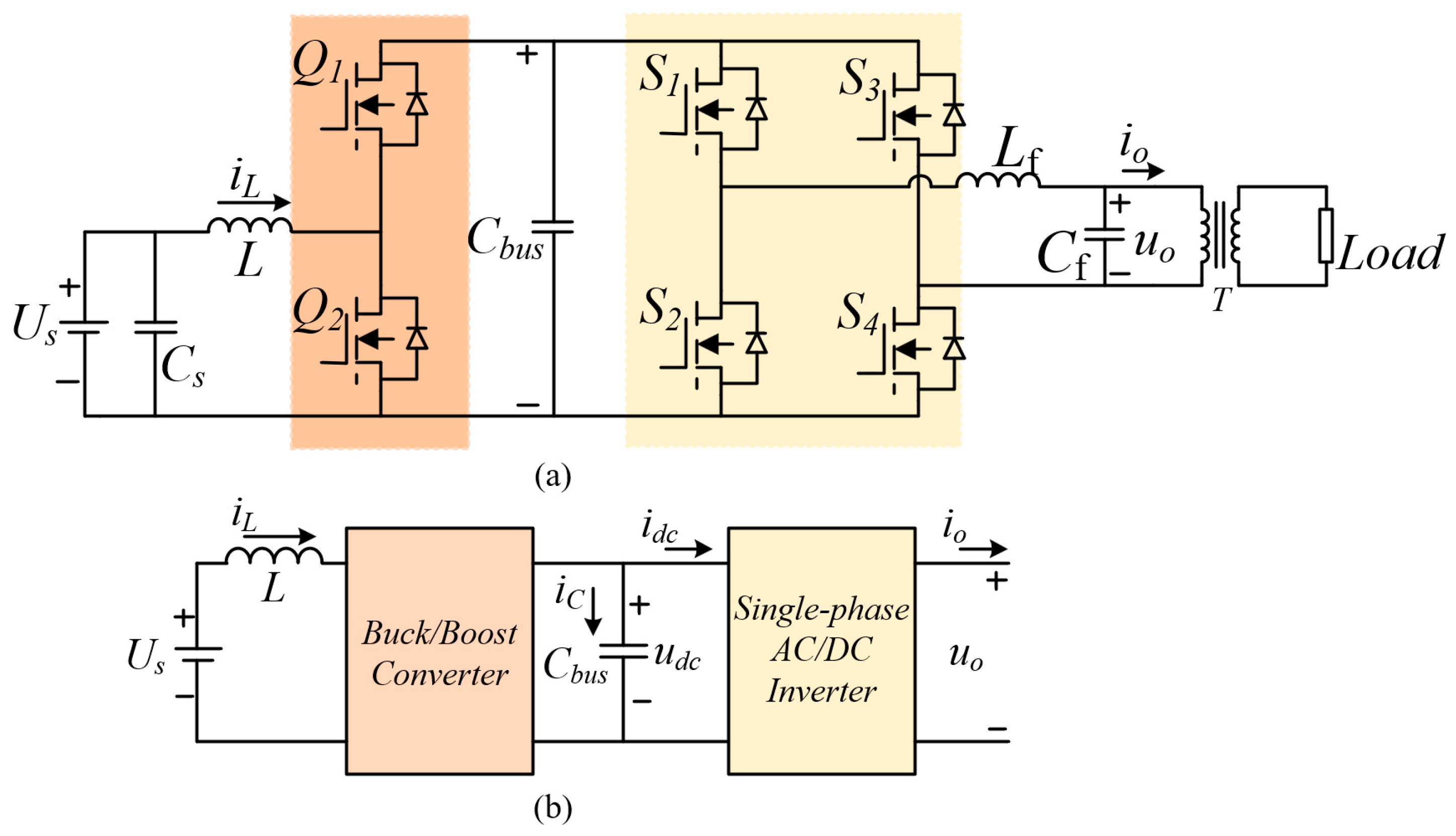
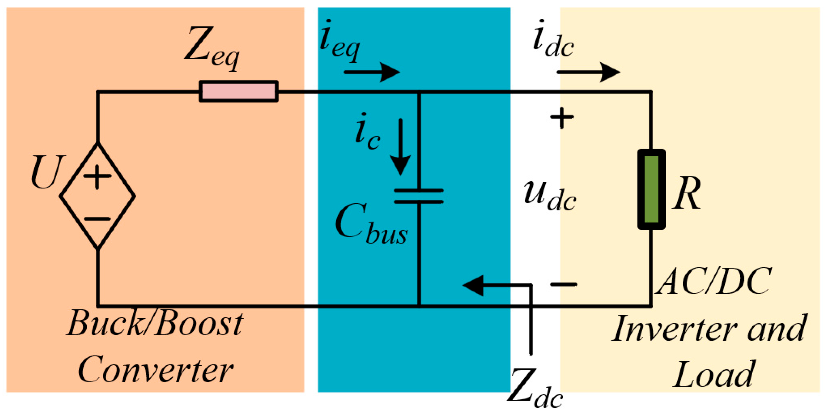
2.1. Generation and Propagation Mechanism of the SRCs

Figure 2a shows the simplified topology of the dynamic voltage restorer (DVR) mitigation device. The DC bus capacitor C b u s connects the front-stage buck/boost converter with the rear-stage DC-AC inverter. The input side ( U s ) is typically connected to the ES or batteries, while the output side ( u o ) interfaces with sensitive loads through a transformer. To streamline the design and analysis process, the transformer is assumed to be ideal, and the configuration in Figure 2a can be further simplified to Figure 2b.
Under ideal conditions, u o is the output voltage of the DVR, and it is a sinusoidal wave. Its expression is:
u o = U o sin ( ω 0 t + φ ) = U o sin ( 2 π f 0 t + φ ) ,
where U o is the amplitude of u o . f 0 is the frequency of u o . The output current i o is represented as
i o = I o sin ( 2 π f 0 t + φ ) ,
where I o is the amplitude of i o . The instantaneous output power P o can be expressed as
P o = u o i o = 1 2 U o I o cos φ D C 1 2 U o I o cos ( 2 π · 2 f 0 t + φ ) A C ,
From Equation (3), it can be concluded that P o contains not only a DC part but also an AC part with a frequency of 2 f 0 .
Under normal operating conditions, the DC bus voltage ripple is typically minimal and can, thus, be approximated as a constant. Furthermore, the input current i d c can be derived as:
i d c = P o u d c = U o I o 2 u d c cos φ U o I o 2 u d c cos ( 2 ω 0 t + φ ) = I d c i S R C s ,
From Equation (4), it can be observed that i d c contains not only a DC part I d c but also an AC part i S R C s with a frequency of 2 f 0 . Consequently, the AC part i S R C s propagates to the DC bus, introducing a current ripple at 2 f 0 in the capacitor C b u s . Under constant input voltage conditions, the SRCs necessarily manifest within the input current i L .

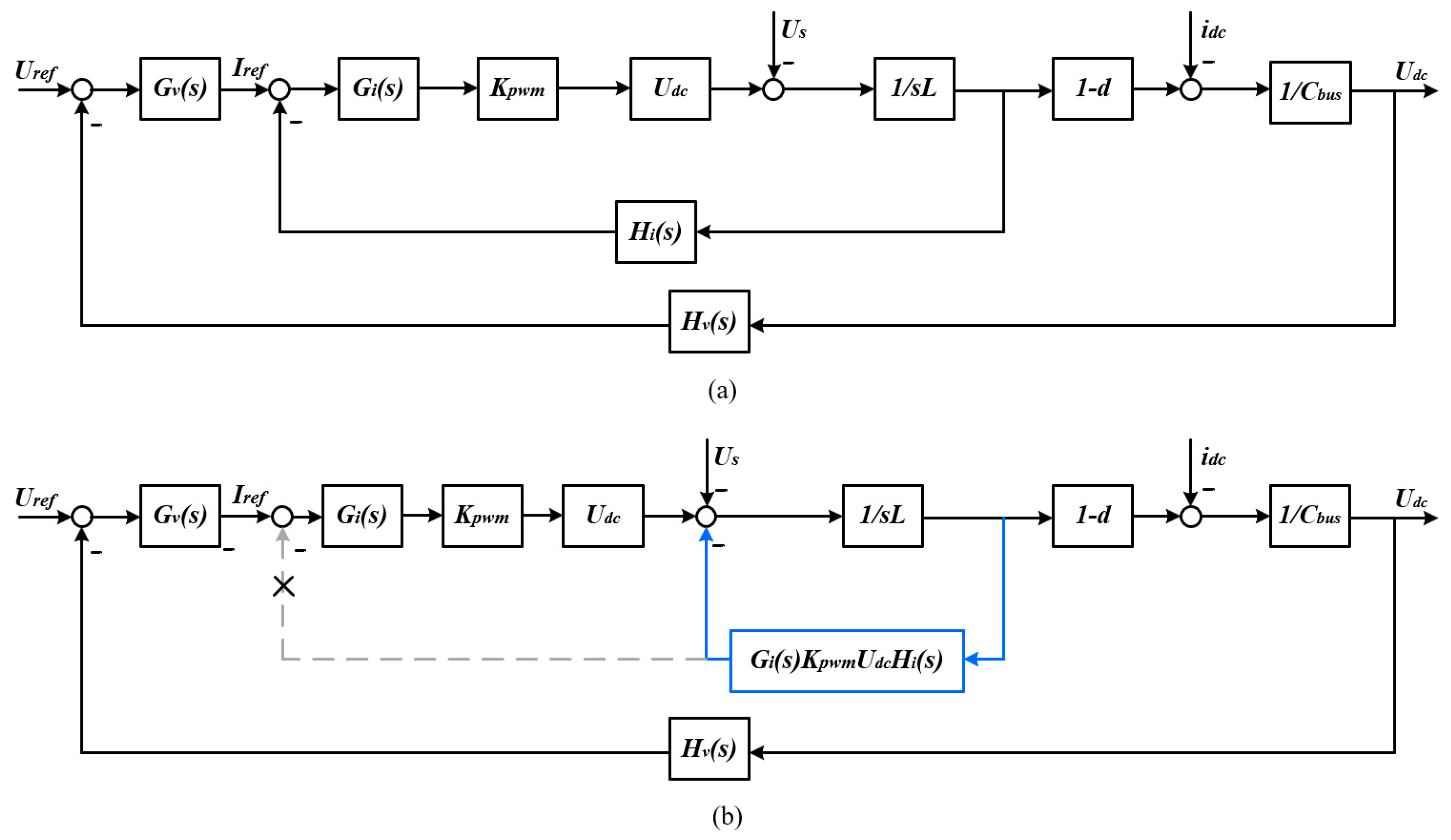
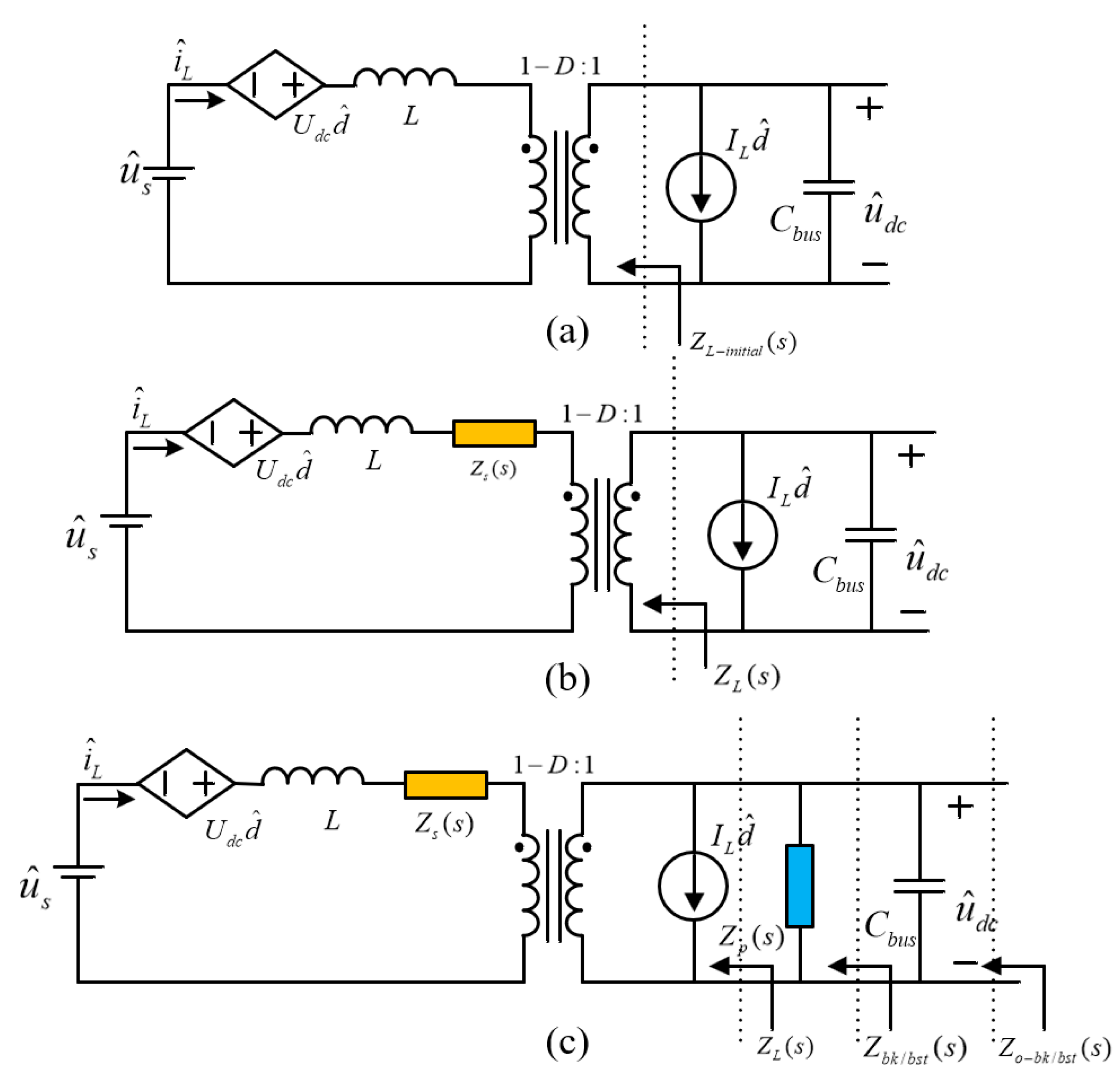
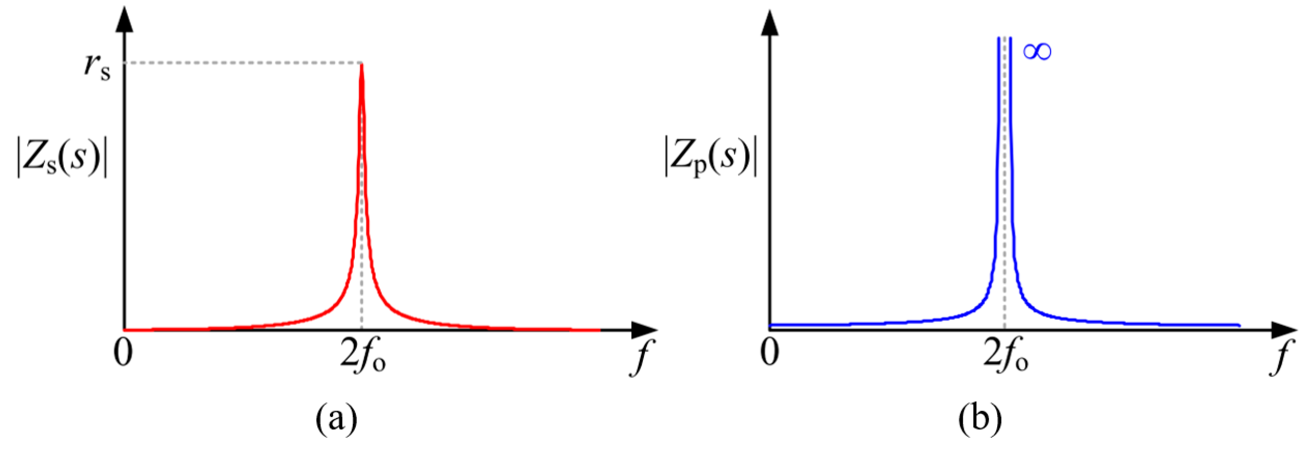
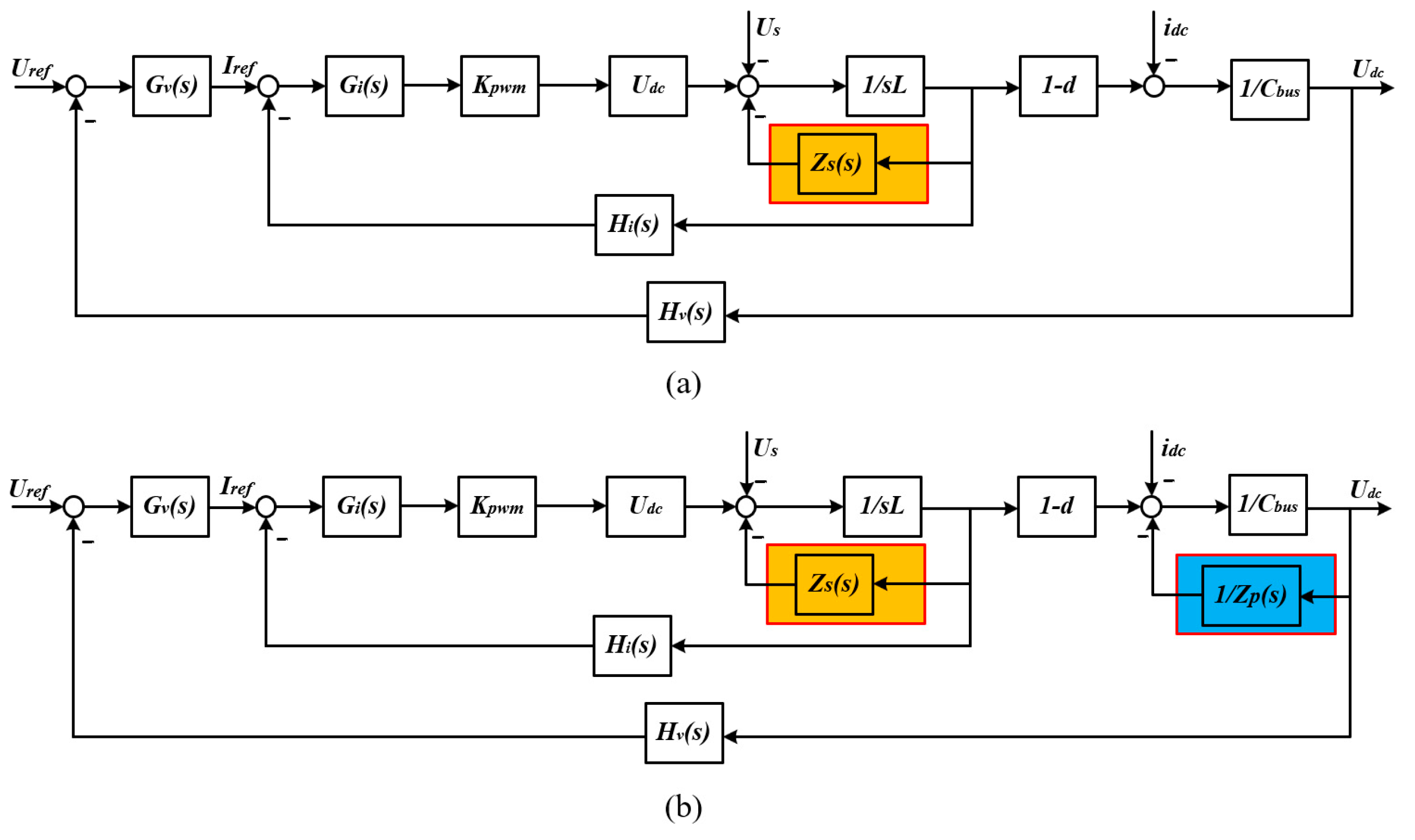
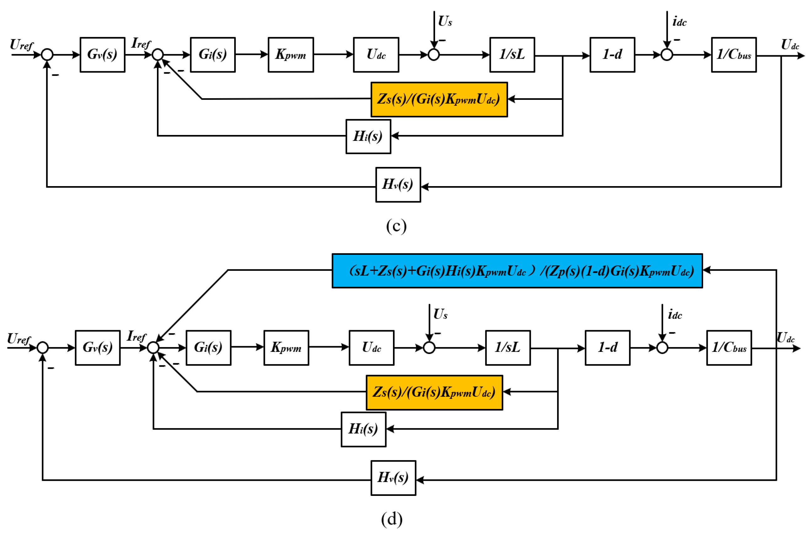
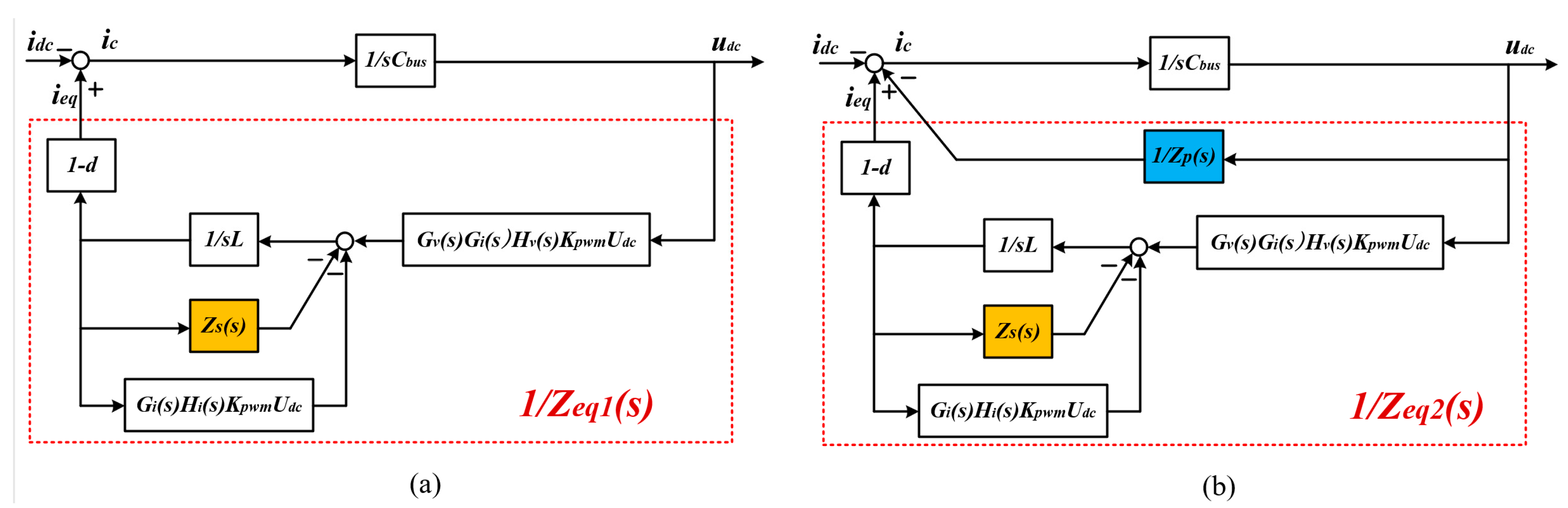
2.2. Suppression Method of SRCs Based on Virtual Impedance

Figure 3a gives the control scheme employing dual feedback loops (voltage and current) for the front-stage converter. G v s and G i s are PI controllers to regulate DC bus voltage u d c and inductor current i L , respectively. d is the duty cycle. H v ( s ) and H i ( s ) represent the sampling functions of u d c and i L . The control structure after equivalent transformation is shown in Figure 3b.
Figure 4a presents the converter’s small-signal model established via state–space averaging methodology. The dominant approach of suppressing the SRCs is to increase the impedance magnitude of Z b k / b s t ( s ) at 2 f 0 or to reduce the magnitude of 1 / s C b u s , the latter of which involves increasing the bus capacitor’s capacity. When the magnitude of Z b k / b s t ( s ) is greater than that of 1 / s C b u s at 2 f 0 , the SRCs will flow into C b u s rather than the input side. Therefore, the proposed methods introduce the virtual series impedance (VSI) Z s ( s ) in the converter’s inductive network (Figure 4b) to increase the magnitude of Z b k / b s t ( s ) at 2 f 0 . Concurrently, to reduce the impedance of 1 / s C b u s at 2 f 0 and to address the fluctuation in the DC bus voltage during variations in the load, it is necessary to minimize the buck/boost converter’s closed-loop output impedance. This is achieved through the virtual parallel impedance (VPI) Z p ( s ) implementation detailed in Figure 4c. Z p ( s ) should have a low impedance at non- 2 f 0 and an open-circuit characteristic at 2 f 0 . The required Z s ( s ) and Z p ( s ) are shown in Figure 5.
Figure 6a,b illustrate the virtual impedance control structure for the front-stage buck/boost converter, derived from Figure 3 and Figure 4b. By relocating the inductor current and bus voltage feedback nodes to the output terminal of the voltage regulator G v ( s ) and optimizing their transfer functions, the equivalent control diagrams are generated, as shown in Figure 6c,d. These configurations reveal that VSI and VPI are implemented via dedicated feedback loops for current and voltage regulation, respectively.

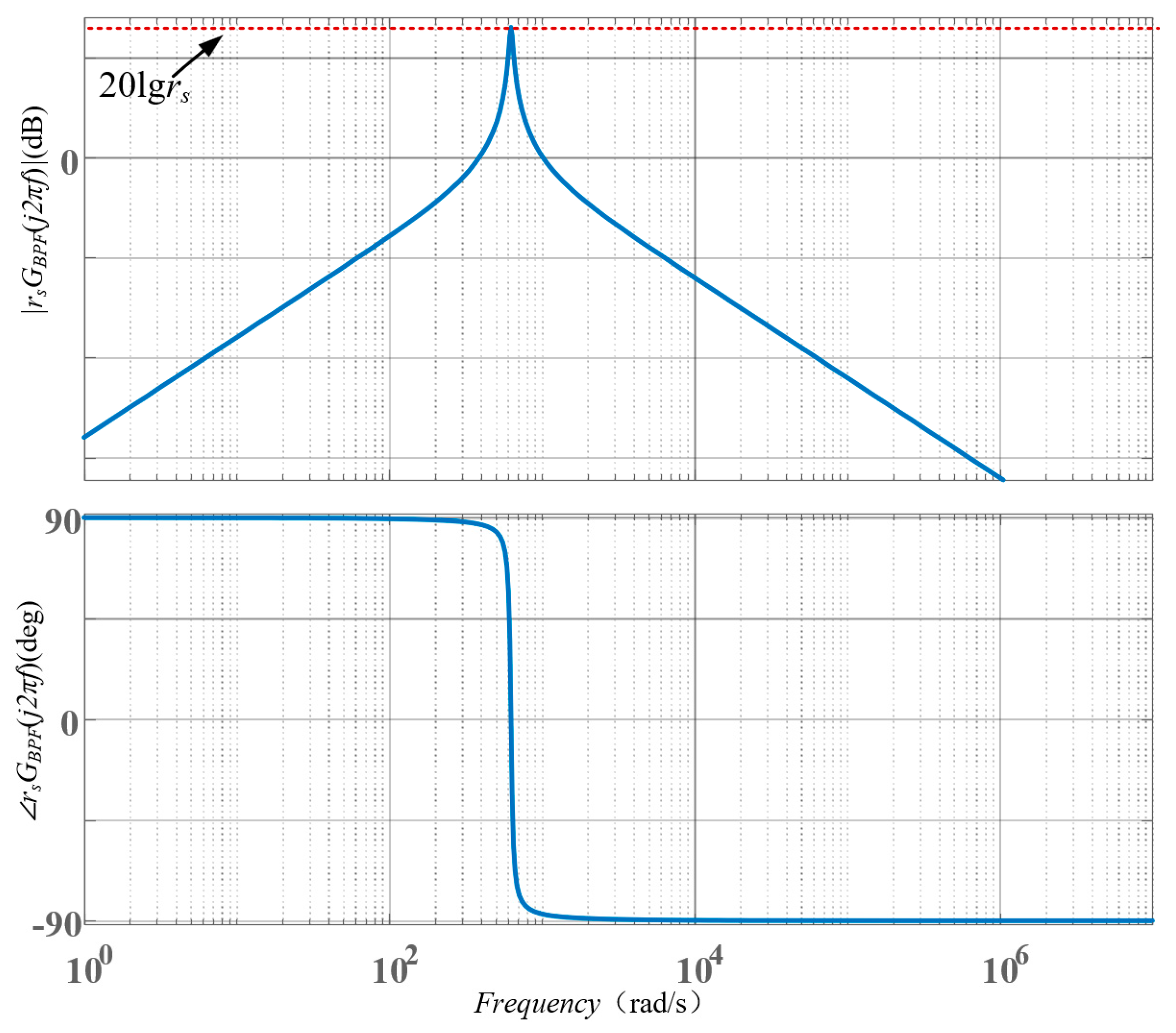
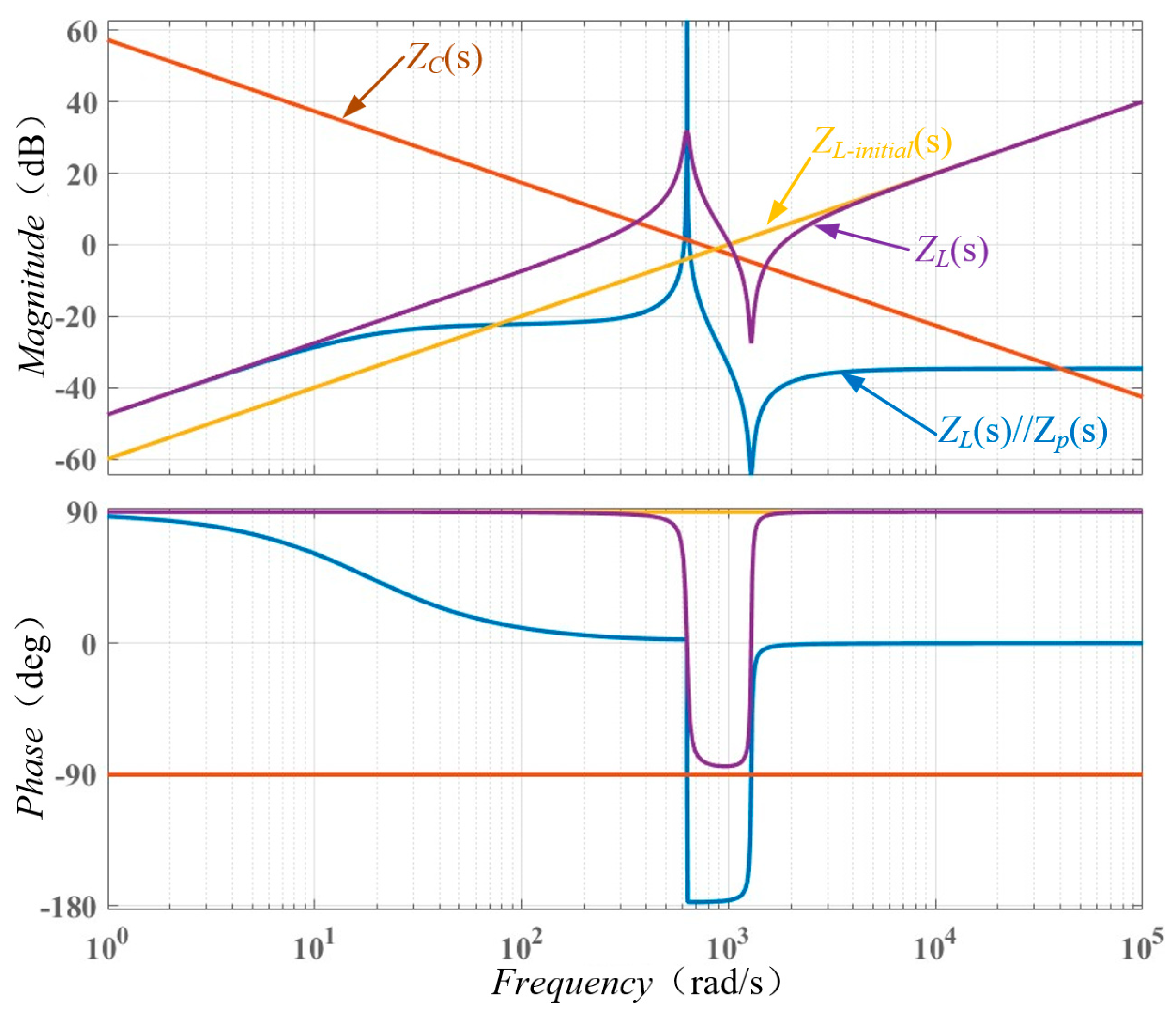
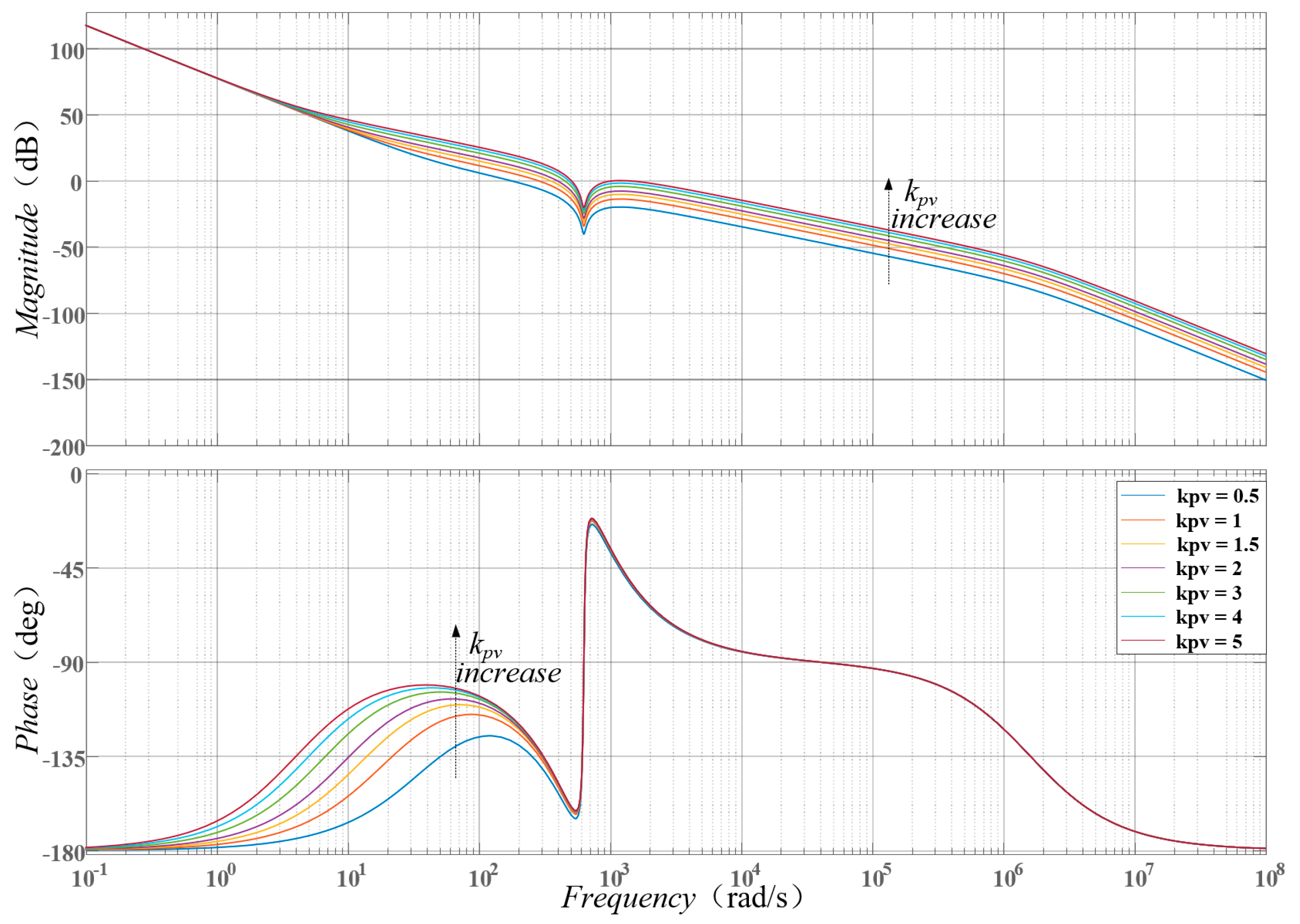
3. Virtual Impedance Selection and Parameter Design
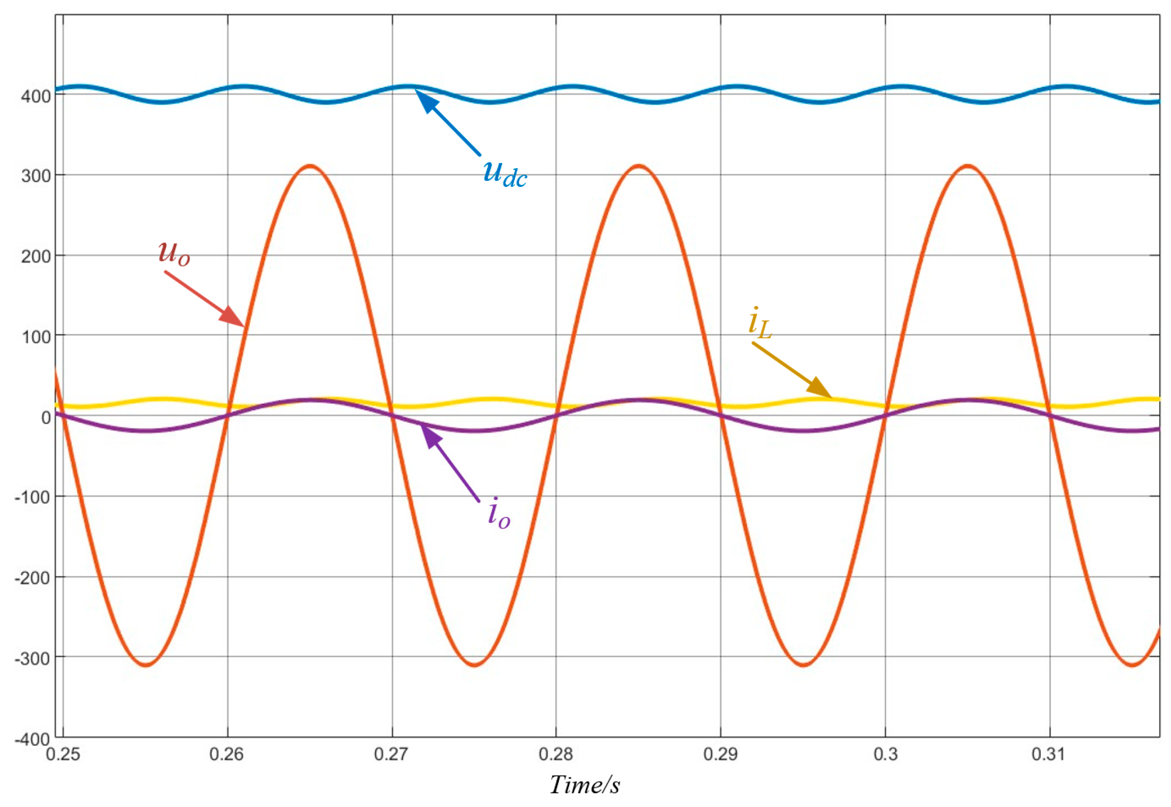
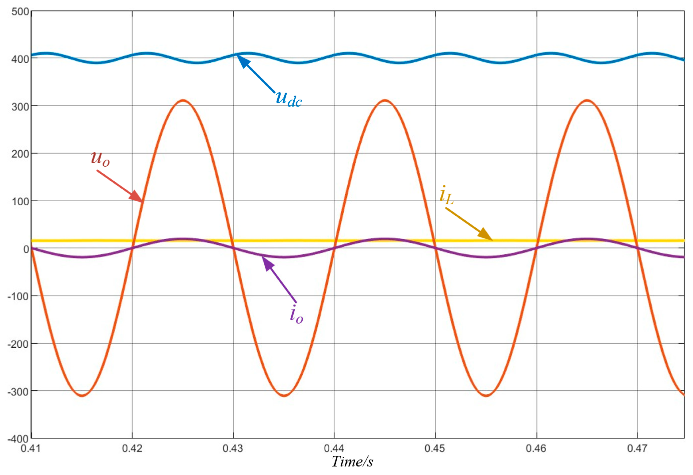
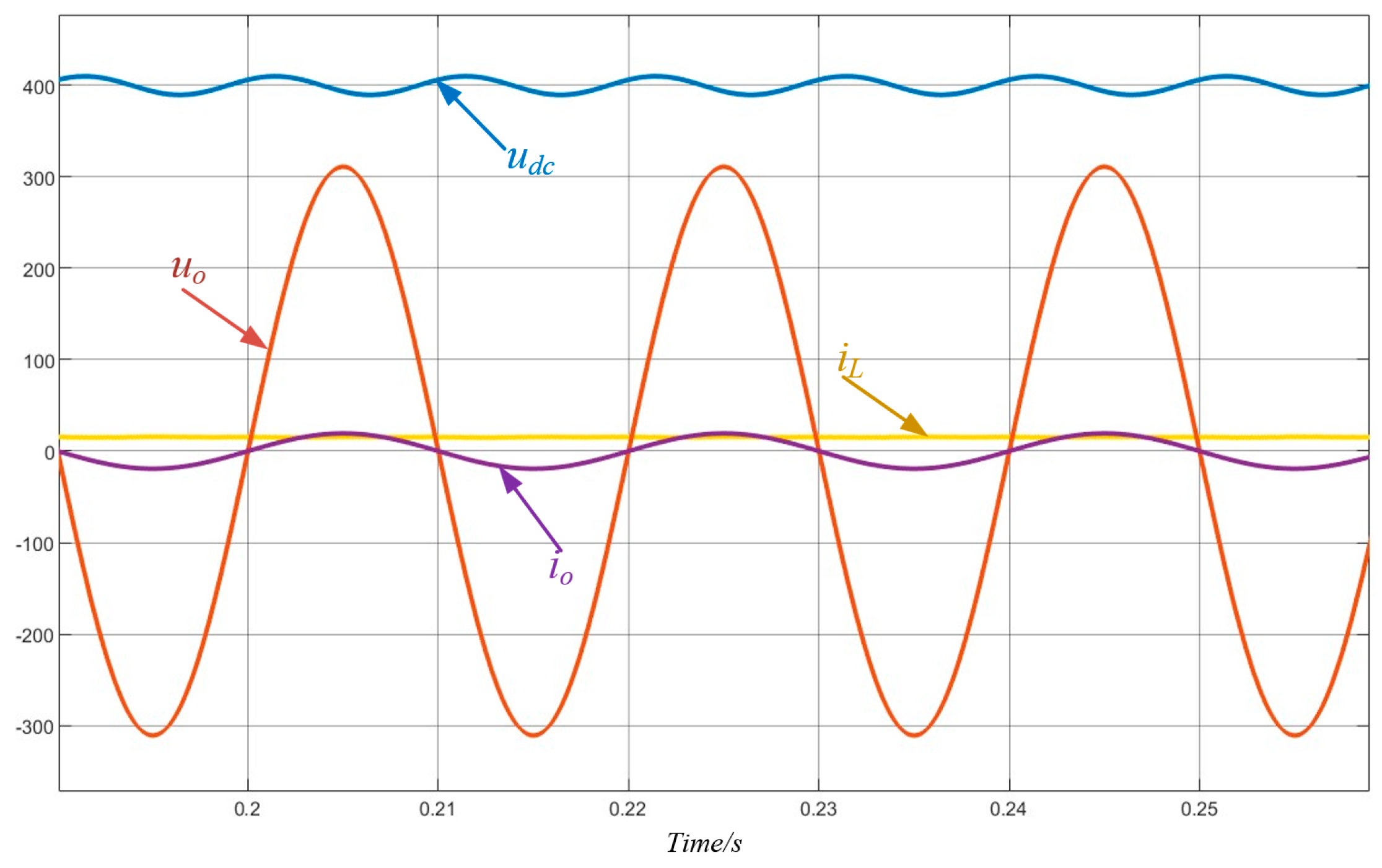
In Figure 5, according to the amplitude–frequency characteristic requirements, Z s ( s ) = r s G B P F ( s ) is the expression of the VSI proposed in this study, where r s is a virtual resistor and G B P F ( s ) is a bandpass filter, and its expression is:
G B P F ( s ) = s / ( Q B P F · ω B P F ) s / ω B P F 2 + s / ( Q B P F · ω B P F ) + 1 ,
where Q B P F is the quality factor. ω B P F = 2 π · 2 f 0 and 2 f 0 are the center frequency.
Figure 7 shows the Bode plot of r s G B P F ( s ) , and it can be seen that at 2 f 0 , r s G B P F ( s ) behaves as a high-magnitude resistor, while at other frequencies, the magnitude is relatively small. Due to the non-ideal reasons of an actual bandpass filter, when f < 2 f 0 , it exhibits an inductive nature; when f > 2 f 0 , it exhibits a capacitive nature.
In Figure 4c, let u ^ s = 0 and d ^ = 0 ; the expression of Z L ( s ) after introducing Z s ( s ) = r s G B P F ( s ) can be obtained:
Z L ( s ) = 1 ( 1 d ) 2 ( r s G B P F ( s ) + s L ) ,
When the virtual impedance is not introduced, the impedance of the inductor branch in the initial state is Z L i n i t i a l ( s ) , and its expression is:
Z L i n i t i a l ( s ) = s L ( 1 d ) 2 ,
Based on Equations (6) and (7), the Bode plots of Z L ( s ) and Z L i n i t i a l ( s ) can be drawn, as shown in Figure 8. It can be observed that after introducing r s G B P F ( s ) into the inductor branch, the impedance magnitude of Z L ( s ) at 2 f 0 significantly increases, surpassing the capacitive reactance of C b u s . This effectively inhibits the propagation of second harmonic components in i d c of the rear-stage DC-AC inverter back to the front-stage buck/boost converter. As mentioned earlier, when f > 2 f 0 , r s G B P F ( s ) exhibits capacitive behavior, it causes a series resonance with L at frequencies higher than 2 f 0 , resulting in a downward resonance peak on the magnitude–frequency characteristic curve of Z L ( s ) .
To decrease the impedance of 1 / s C b u s at 2 f 0 and to minimize the fluctuation in the DC bus voltage upon variations in the load, the output impedance Z o b k / b s t of the converter should be as small as possible. It can be expressed as:
Z o b k / b s t = Z o b k / b s t o p e n ( s ) 1 + T v b k / b s t ( s ) ,
where T v b k / b s t ( s ) represents the voltage regulation loop gain in the control strategy of the front-stage buck/boost converter. Thus, reducing Z o b k / b s t can be achieved by decreasing Z o b k / b s t .
In Figure 4c, let u ^ s = 0 and d ^ = 0 ; the expression of Z o b k / b s t o p e n ( s ) after introducing them can be obtained:
Z o b k / b s t o p e n ( s ) = Z L ( s ) / / Z p ( s ) / / Z C ( s ) ,
For any inductive-resistive parallel network, its parallel impedance can be represented in the form of an inductor’s reactance in series with a low-pass filter. Hence, Equation (9) can be simplified as:
Z o b k / b s t o p e n ( s ) = ( Z L ( s ) · G L P F ( s ) ) / / Z C ( s ) ,
To minimize the magnitude of Z o b k / b s t o p e n s as much as possible, the cutoff frequency of G L P F ( s ) must be low and far from 2 f 0 . At the same time, to preserve the buck/boost converter’s output impedance at 2 f 0 , G N ( s ) , with a center frequency of 2 f 0 , must be introduced into G L P F ( s ) . Therefore, the expression of G L P F ( s ) is:
G L P F ( s ) = ω L P F ω L P F + s · G N ( s ) ,
where ω L P F is the cutoff frequency of G L P F ( s ) , and it satisfies:
ω L P F 2 π · 2 f 0 ,
The expression of G N ( s ) is:
G N ( s ) = ( s / ω N ) 2 + 1 ( s / ω N ) 2 + s / ( Q N · ω N ) + 1 ,
where Q N is the quality factor, and ω N = 2 π · 2 f 0 .
By substituting Equation (6) into (9)–(11), the following can be obtained:
Z p ( s ) = s L + r s G B P F ( s ) ( 1 d ) 2 · ω L P F s G N ( s ) ,
After introducing Z s ( s ) = r s G B P F ( s ) , at 2 f 0 , we have:
Z L ( j 2 π · 2 f 0 ) = ( j 2 π · 2 f 0 · L + r s ) ( 1 d ) 2 Z C ( j 2 π · 2 f 0 ) = 1 2 π · 2 f 0 · C b u s ,
The inductive reactance of L at 2 f 0 is much smaller than r s ; so, from Equation (15), we can obtain:
( j 2 π · 2 f 0 · L + r s ) ( 1 d ) 2 r s ( 1 d ) 2 1 2 π · 2 f 0 · C b u s ,
Further, it yields:
( 1 d ) 2 r s C b u s 2 π · 2 f 0 ,
According to Equations (12) and (17), ω L P F can be taken as ( 1 d ) 2 / r s C b u s . Substituting this into Equation (13), we have:
Z p ( s ) = s L + r s G B P F ( s ) s · r s C b u s · G N ( s ) ,
Based on Thevenin’s theory, the front-stage buck/boost converter can be modeled as a two-port network and equivalently represented by a voltage source in series with an impedance. Furthermore, when higher-order harmonic components are neglected, load and the rear-stage single-phase DC/AC inverter can be equivalently substituted with a purely resistive load. The simplified equivalent representation is shown in Figure 9.
To obtain Z e q ( s ) , U s and V r e f in Figure 6c,d are set to zero. The control structure of the front-stage converter with i d c as the input variable is shown in Figure 10. The equivalent impedance 1 / Z e q of the converter is represented in the red dashed box. When only VSI is introduced, the equivalent admittance is 1 / Z e q 1 ( s ) , and when VSI and VPI are introduced, the equivalent admittance is 1 / Z e q 2 ( s ) . The expressions for both are:
1 Z e q 1 = ( 1 d ) G v ( s ) H v ( s ) G i ( s ) K P W M U d c s L + Z s ( s ) + G i ( s ) H i ( s ) K P W M U d c ,
1 Z e q 2 = ( 1 d ) G v ( s ) G i ( s ) K P W M U d c s L + Z s ( s ) + G i ( s ) H i ( s ) K P W M U d c + 1 Z p ( s ) ,
Therefore, the equivalent output impedance Z d c of the bus capacitor and front-stage buck/boost converter is given as:
Z d c ( s ) = Z e q ( s ) / / 1 s C b u s ,
In order to balance the system’s dynamic performance, the magnitude of Z e q ( s ) should be large at 2 f 0 , while it should be as small as possible at non- 2 f 0 . Z d c will be lower as Z e q decreases, thereby reducing the fluctuation in the DC bus voltage u d c .
Z d c ( s ) can be adjusted by modifying G v ( s ) . G v ( s ) is a PI controller, and its expression is:
G v ( s ) = k p v + k i v s ,
It is reasonable to change Z e q ( s ) by adjusting k p v while keeping k i v fixed. This is because k p v has a more significant contribution to the magnitude of Z e q ( s ) compared to k i v . After introducing VSI, the open-loop transfer function T ( s ) can be expressed as:
T ( s ) = 1 Z e q 1 ( s ) · 1 s C b u s = ( 1 d ) G v ( s ) H v ( s ) G i ( s ) K P W M U d c s L + Z s ( s ) + G i ( s ) H i ( s ) K P W M U d c · 1 s C b u s ,
In Figure 11, the bandwidth and cutoff frequency of T ( s ) exhibit a positive correlation with k p v . Additionally, a Nyquist diagram of T ( s ) is shown in Figure 12, and it can be observed that the phase margin (PM) decreases as k p v increases. When k p v is 0.5, the PM is 52.4 deg, while when k p v is 5, the PM is 20.8 deg. To meet general engineering requirements while considering bandwidth, k p v can be set to 1, at which point P M = 45.6 deg .
When VSI and VPI are introduced, the equivalent impedance of the converter Z e q is shown in Figure 13, and it is illustrated that while the equivalent impedance Z e q at 2 f 0 increases, the impedance at non- 2 f 0 is reduced. This effectively mitigates the SRCs while also reducing the fluctuation in the DC bus voltage upon variations in the load.

4. Results Analysis

4.1. Simulation Results

A simulation model of the DVR voltage sag mitigation system is built in MATLAB R2024a based on the parameters in Table 1. The simulation results are shown in Figure 14, Figure 15 and Figure 16.
Figure 14 presents the main waveforms under conventional dual feedback loop (voltage and current) control in steady state. u o and i o are the output voltage and current of the system, u d c is the bus capacitor voltage, and i L is the input-side inductor current. Both u o and i o are sinusoidal waveforms at a frequency of 50 Hz, but the frequency of i L is clearly twice that of u o and i o . This indicates that there is a 100 Hz harmonic current component present in i L .
Figure 15 and Figure 16 show the key waveforms after introducing the virtual impedance methods proposed in this study. It is clearly seen that the SRCs in i L are greatly reduced and have become a smooth DC waveform. Table 2 provides the results of the FFT analysis of the input-side inductor current i L for the three control strategies. When only VSI is introduced, the percentage of SRCs relative to the average value decreases from 31.72% to 1.04%. When VSI and VPI are introduced, the percentage of SRCs relative to the average value is 1.07%. When using the method proposed in reference [24], the percentage of SRCs relative to the average value is 2.894%. These results demonstrate that most of the SRCs have been effectively suppressed. Furthermore, compared to the suppression method in [24], the proposed methods demonstrate better performance in suppressing the SRCs.
However, compared to the conventional dual feedback loop (voltage and current) control strategy and the proposed control strategy with VSI, the proposed control strategy with VSI and VPI increases the fourth harmonic content. The percentage of the fourth harmonic relative to the average value increases from 0.22% and 0.19% to 1.16%. This phenomenon is related to the equivalent impedance Z e q ( s ) of the front-stage buck/boost converter after the introduction of the parallel impedance. Figure 13 shows Z e q ( s ) after introducing both types of virtual impedance. In the case where VSI and VPI are introduced, a downward resonance peak is observed at 4 f 0 in the amplitude–frequency characteristic curve. It is preliminarily speculated that this peak at 4 f 0 leads to an increase in the fourth harmonic content in the input current i L .

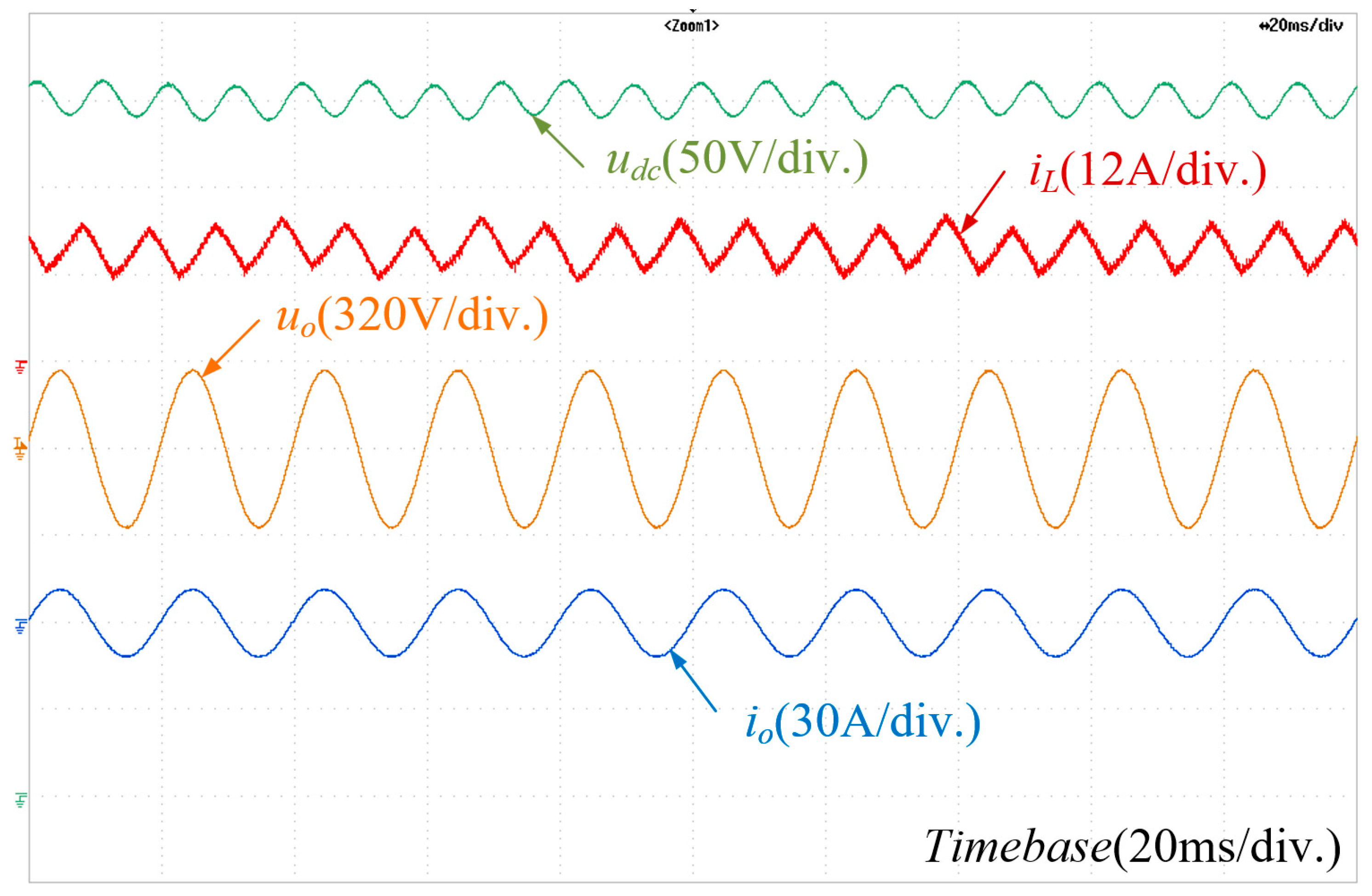
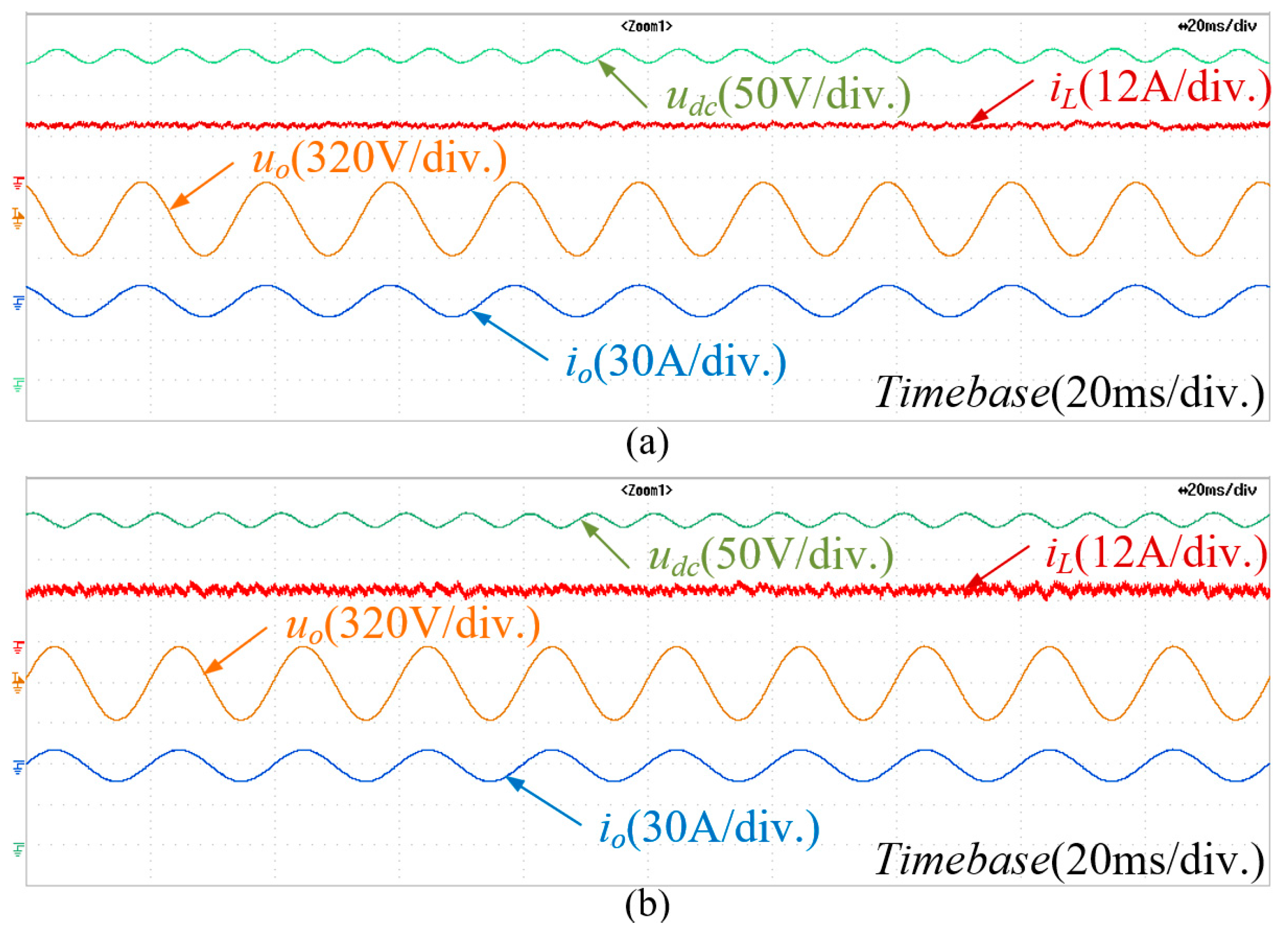
4.2. Experimental Verification

A 3 kW dynamic voltage restorer experimental prototype was designed and fabricated in the laboratory based on the main parameters in Table 1. The DSP TMS320F82335 is used as the main controller.
The load is purely resistive. Figure 17 and Figure 18 show the key voltage and current waveforms of the DVR system under full load conditions. Both u o and i o are sinusoidal waveforms at a power frequency of 50 Hz. The voltage and current waveforms before compensation are shown in Figure 17. Before compensation, the frequency of i L is clearly twice that of u o and i o , indicating the presence of significant second-order harmonic components in it. The key waveforms under the proposed methods in this study are shown in Figure 18, where i L becomes a smooth DC waveform, and the SRCs are effectively suppressed. The peak ripple of i L decreases from 5.9 A to 1.2 A and from 5.9 A to 1.1 A, while the ripple factor of i L decreases from 37.6% to 7.66% and 7.2%, respectively. The experimental results obtained well validate the rationality and correctness of Equations (5)–(18).
The input current i L data obtained from the oscilloscope are imported into MATLAB R2024a’s FFT toolbox for harmonic content analysis. The results are shown in Table 3. The DC components of the three methods are similar to the average values of i L read from the oscilloscope. When using the method proposed in [24], the percentage of SRCs relative to the average value is 2.11%. After introducing virtual impedance, the secondary ripple content in i L is significantly reduced, with the percentage of SRCs decreasing from 39.64% to 1.74% and 1.78% and the secondary harmonic content being less than 2%. There are still minor fluctuations in the waveform, which are caused by parasitic inductance, parasitic capacitance, and noise in the circuits.
However, when VSI and VPI are introduced simultaneously, the fourth harmonic content increases, which aligns with the conclusions derived from the simulation. The percentage of the fourth harmonic relative to the average value increases from 0.54% and 0.64% to 1.62%. This phenomenon occurs due to a downward peak in the frequency response of the front-stage buck/boost converter’s equivalent impedance at 4 f 0 when VSI and VPI are applied, resulting in resonance at 4 f 0 in the input current.

5. Conclusions

In response to the double-frequency ripple phenomenon observed in existing two-stage single-phase DVR voltage sag mitigation devices, this study introduces the VSI and VPI methods to suppress SRCs, based on the dual feedback loop (voltage and current) control strategy of the front-stage buck/boost converter. The virtual impedances can be realized in the current and voltage sampling loops through equivalent transformation. Compared to existing schemes, the proposed methods offer the advantages of being fast, stable, and reliable, while the virtual impedance auxiliary control strategy is flexible and simple to implement. The feasibility and stability of this strategy were verified using a 3 kW DVR prototype. When applying the two virtual impedance methods, the second harmonic content was reduced from 39.64% to 1.74% and 1.78%, respectively. However, after introducing VSI and VPI, the fourth harmonic content in the input current i L increased. This may be due to a downward resonance peak in the equivalent impedance of the buck/boost converter at 4 f 0 caused by the introduction of VSI and VPI.
The current work still has certain limitations, which will be key focuses for future research:
(1)
The fundamental mechanism behind the increased fourth harmonic content in the input current i L after introducing VSI and VPI requires further investigation. This study only proposed a possible explanation, which remains unverified.
(2)
In real-world applications, DVRs typically encounter complex conditions, such as grid harmonics, nonlinear loads, and load surges, which may limit the effectiveness of virtual impedance. It is necessary to adjust the virtual impedance parameters according to the impedance characteristics of different actual circuits.
(3)
Practical applications involve numerous uncertainties and variable conditions. Ensuring and improving the reliability and operational efficiency of DVRs under real-world operating scenarios are highly worthy of research. In subsequent studies, the risk aversion and distributed optimization methods from reference [28] can serve as important guidance.
(4)
In the practical application and promotion of DVRs, the cost, lifespan, and reliability of energy storage devices are major concerns for end-users. Reducing investment costs and extending service life to expand DVR adoption will be key research priorities. The shared energy storage service and optimal configuration methods proposed in reference [29] can effectively address these needs and provide critical guidance for our future work.

Author Contributions

Conceptualization, G.H. and J.L.; methodology, Q.Z.; software, Q.Z.; validation, Q.Z. and J.L.; formal analysis, Q.S.; investigation, Q.S.; resources, G.H.; data curation, W.L.; writing—original draft preparation, Q.Z.; writing—review and editing, J.L.; visualization, G.H.; supervision, J.L.; project administration, J.L.; funding acquisition, G.H. All authors have read and agreed to the published version of the manuscript.

Funding

This research was funded by the Science and Technology Project of Guangdong Power Grid Co., Ltd. (No.030600KC23070021; No.GDKJXM20230914).

Data Availability Statement

Data are contained within the article.

Conflicts of Interest

Authors Guoping Huang, Qiao Shi, Wenqing Li were employed by the company Foshan Power Supply Bureau of Guangdong Power Grid Co., Ltd. The remaining authors declare that the research was conducted in the absence of any commercial or financial relationships that could be construed as a potential conflict of interest. The authors declare that this study received funding from China Southern Power Grid Co., Ltd.

Abbreviations

The following abbreviations are used in this manuscript:
DVRDynamic Voltage Restorer
ESEnergy Storage
SRCsSecond-order Ripple Currents
VSIVirtual Series Impedance
VPIVirtual Parallel Impedance

References

  1. Martinez, J.A.; Arnedo, J.M. Voltage sag studies in distribution networks—Part I: System modeling. IEEE Trans. Power Del. 2006, 21, 1670–1678. [Google Scholar] [CrossRef]
  2. Kaniewski, J.; Fedyczak, Z.; Benysek, G. AC voltage sag/swell compensator based on three-phase hybrid transformer with buck–boost matrix-reactance chopper. IEEE Trans. Ind. Electron. 2014, 61, 3835–3846. [Google Scholar]
  3. Castilla, M.; Miret, J.; Camacho, A.; Matas, J.; de Vicuna, L. Voltage support control strategies for static synchronous compensators under unbalanced voltage sags. IEEE Trans. Ind. Electron. 2014, 61, 808–820. [Google Scholar] [CrossRef]
  4. Garcia, P.M.; Mancilla, F.; Ramirez, J.M. Per-sequence vector switching matrix converter modules for voltage regulation. IEEE Trans. Ind. Electron. 2013, 60, 5411–5421. [Google Scholar] [CrossRef]
  5. Kumar, C.; Mishra, M. A multifunctional DSTATCOM operating under stiff source. IEEE Trans. Ind. Electron. 2014, 61, 3131–3136. [Google Scholar]
  6. Kanjiya, P.; Singh, B.; Chandra, A.; Al-Haddad, K. SRF theory revisited to control self-supported dynamic voltage restorer (DVR) for unbalanced and nonlinear loads. IEEE Trans. Ind. Appl. 2013, 49, 2330–2340. [Google Scholar]
  7. Wessels, C.; Gebhardt, F.; Fuchs, F.W. Fault ride-through of a DFIG wind turbine using a dynamic voltage restorer during symmetrical and asymmetrical grid faults. IEEE Trans. Power Electron. 2011, 26, 807–815. [Google Scholar]
  8. Bala, S.; Tengnér, T.; Rosenfeld, P.; Delince, F. The effect of low frequency current ripple on the performance of a Lithium Iron Phosphate (LFP) battery energy storage system. In Proceedings of the 2012 IEEE Energy Conversion Congress and Exposition (ECCE), Raleigh, NC, USA, 15–20 September 2012; pp. 3485–3492. [Google Scholar] [CrossRef]
  9. Liu, C.; Wang, J.; Colombage, K.; Gould, C.; Sen, B.; Stone, D. Current ripple reduction in 4kW LLC resonant converter based battery charger for electric vehicles. In Proceedings of the 2015 IEEE Energy Conversion Congress and Exposition (ECCE), Montreal, QC, Canada, 20–24 September 2015; pp. 6014–6021. [Google Scholar] [CrossRef]
  10. Qian, K.; Zhou, C.; Yuan, Y.; Allan, M. Temperature effect on electric vehicle battery cycle life in Vehicle-to-grid applications. In Proceedings of the 4th China International Conference on Electricity Distribution (CICED 2010), Nanjing, China, 13–16 September 2010; pp. 1–6. [Google Scholar]
  11. Sun, Y.; Liu, Y.; Su, M.; Xiong, W.; Yang, J. Review of active power decoupling topologies in single-phase systems. IEEE Trans. Power Electron. 2016, 31, 4778–4794. [Google Scholar]
  12. Tang, Y.; Blaabjerg, F.; Loh, P.C.; Jin, C.; Wang, P. Decoupling of fluctuating power in single-phase systems through a symmetrical half-bridge circuit. IEEE Trans. Power Electron. 2015, 30, 1855–1865. [Google Scholar]
  13. Lin, Z.; He, L.; Zhou, H. A second harmonic current suppressing method based on negative-order capacitor. IEEE Trans. Power Electron. 2022, 37, 8465–8475. [Google Scholar]
  14. Almeida, P.S.; Bender, V.C.; Braga, H.A.C.; Costa, M.A.D.; Marchesan, T.B.; Alonso, J.M. Static and dynamic photoelectrothermal modeling of led lamps including low-frequency current ripple effects. IEEE Trans. Power Electron. 2015, 30, 3841–3851. [Google Scholar] [CrossRef]
  15. Wang, H.; Blaabjerg, F. Reliability of capacitors for dc-link applications in power electronic converters—An overview. IEEE Trans. Ind. Appl. 2014, 50, 3569–3578. [Google Scholar] [CrossRef]
  16. Liu, C.; Lai, J.-S. Low frequency current ripple reduction technique with active control in a fuel cell power system with inverter load. IEEE Trans. Power Electron. 2007, 22, 1429–1436. [Google Scholar] [CrossRef]
  17. Wang, J.; Ji, B.; Lu, X.; Deng, X.; Zhang, F.; Gong, C. Steady-state and dynamic input current low-frequency ripple evaluation and reduction in two-stage single-phase inverters with back current gain model. IEEE Trans. Power Electron. 2014, 29, 4247–4260. [Google Scholar] [CrossRef]
  18. Ksiazek, P.F.; Ordonez, M. Swinging bus technique for ripple current elimination in fuel cell power conversion. IEEE Trans. Power Electron. 2014, 29, 170–178. [Google Scholar] [CrossRef]
  19. Zhang, L.; Ren, X.; Ruan, X. A bandpass filter incorporated into the inductor current feedback path for improving dynamic performance of the front-end DC–DC converter two-stage inverter. IEEE Trans. Ind. Electron. 2014, 61, 2316–2325. [Google Scholar] [CrossRef]
  20. Chaturvedi, S.; Fulwani, D.; Patel, D. Dynamic Virtual Impedance-Based Second-Order Ripple Regulation in DC Microgrids. IEEE J. Emerg. Sel. Top. Power Electron. 2022, 10, 1075–1083. [Google Scholar] [CrossRef]
  21. Zhu, G.; Ruan, X.; Zhang, L.; Wang, X. On the reduction of second harmonic current and improvement of dynamic response for two-stage single-phase inverter. IEEE Trans. Power Electron. 2015, 30, 1028–1041. [Google Scholar] [CrossRef]
  22. Zhang, L.; Ruan, X.; Ren, X. Second-harmonic current reduction and dynamic performance improvement in the two-stage inverters: An output impedance perspective. IEEE Trans. Ind. Electron. 2015, 62, 394–404. [Google Scholar] [CrossRef]
  23. Zhou, H.; He, L. Impedance-Edited Multiple Low-Frequency Harmonic Current Adaptive Suppression. IEEE Trans. Power Electron. 2023, 38, 7022–7033. [Google Scholar] [CrossRef]
  24. Zhou, H.; He, L.; Yang, Z.; Lin, Z. Virtual Fractional-Order-Inductor Based Second Harmonic Current Suppression Method. IEEE Trans. Ind. Electron. 2024, 71, 8949–8959. [Google Scholar] [CrossRef]
  25. Lei, Y.; Yang, P.; Yu, M. An Improved Deadbeat Control Method for Second Harmonic Current Reduction in Two-Stage Single-Phase Inverter. In Proceedings of the 2022 International Conference on Power Energy Systems and Applications (ICoPESA), Singapore, 25–27 February 2022; pp. 319–325. [Google Scholar]
  26. Liu, G.; Caldognetto, T.; Mattavelli, P.; Magnone, P. Suppression of Second-Order Harmonic Current for Droop-Controlled Distributed Energy Resource Converters in DC Microgrids. IEEE Trans. Ind. Electron. 2020, 67, 358–368. [Google Scholar] [CrossRef]
  27. Wang, Y.; Yang, J.-W.; Kim, W.-J.; Kwon, T.-H.; Lee, T.; Park, S.-J. Second Harmonic Current Suppression and Dynamic Response Improvement for V2G System. IEEE Trans. Power Electron. 2023, 38, 9566–9580. [Google Scholar] [CrossRef]
  28. Zhai, X.; Li, Z.; Li, Z.; Xue, Y.; Chang, X.; Su, J.; Jin, X.; Wang, P.; Sun, H. Risk-averse energy management for integrated electricity and heat systems considering building heating vertical imbalance: An asynchronous decentralized approach. Appl. Energy 2025, 383, 125271. [Google Scholar] [CrossRef]
  29. Zhang, H.; Li, Z.; Xue, Y.; Chang, X.; Su, J.; Wang, P.; Guo, Q.; Sun, H. A Stochastic Bi-Level Optimal Allocation Approach of Intelligent Buildings Considering Energy Storage Sharing Services. IEEE Trans. Consum. Electron. 2024, 70, 5142–5153. [Google Scholar] [CrossRef]
Figure 1. Basic system configuration of DVR.
Energies 18 01896 g001
Figure 2. The configuration of the single-phase DVR mitigation device. (a) The typically simplified topology. (b) The further simplified single-phase two-stage inverter configuration.
Energies 18 01896 g002
Figure 3. The simplified dual feedback loop (voltage and current) control structure of the front-stage converter. (a) Original control structure. (b) After the equivalent transformation.
Energies 18 01896 g003
Figure 4. The small-signal model of the converter. (a) Original configuration. (b) Introducing Z s ( s ) . (c) Introducing Z s ( s ) and Z p ( s ) .
Energies 18 01896 g004
Figure 5. The amplitude–frequency characteristic requirements of the virtual impedance. (a) Z s ( s ) . (b) Z p ( s ) .
Energies 18 01896 g005
Figure 6. Virtual impedance-based control structure for the front-stage buck/boost converters: (a) The compensation scheme of VSI. (b) The compensation scheme of VSI and VPI. (c) The implementation of Z s ( s ) . (d) The implementation of Z p ( s ) .
Energies 18 01896 g006aEnergies 18 01896 g006b
Figure 7. The Bode plots of r s G B P F ( s ) .
Energies 18 01896 g007
Figure 8. The Bode plots of Z L ( s ) , Z L i n i t i a l ( s ) and Z L ( s ) / / Z p ( s ) .
Energies 18 01896 g008
Figure 9. Circuit configuration after using equivalent impedance methods.
Energies 18 01896 g009
Figure 10. The control structure of the front-stage converter with i d c as the input variable. (a) VSI. (b) VSI and VPI.
Energies 18 01896 g010
Figure 11. Bode diagram of T ( s ) with different k p v after introducing VSI.
Energies 18 01896 g011
Figure 12. Nyquist diagram of T ( s ) with different k p v after introducing VSI.
Energies 18 01896 g012
Figure 13. Bode diagram of Z e q ( s ) . (a) Introducing VSI. (b) Introducing VSI and VPI.
Energies 18 01896 g013
Figure 14. Key waveforms with traditional voltage–current dual-loop control.
Energies 18 01896 g014
Figure 15. Key waveforms after introducing VSI.
Energies 18 01896 g015
Figure 16. Key waveforms after introducing VSI and VPI.
Energies 18 01896 g016
Figure 17. Key waveforms with dual feedback loop (voltage and current) control strategy.
Energies 18 01896 g017
Figure 18. Key voltage and current waveforms. (a) Introducing VSI. (b) Introducing VSI and VPI.
Energies 18 01896 g018
Table 1. Main parameters of simulation and prototype.
ParametersSpecifications
Buck/Boost ConverterUbat/V200
fs/kHz10
L/mH0.5
Cbus/mF1.36
Single-phase InverterUac/V311
f0/Hz50
Lf/mH4
Cf/mF0.13
Switching Frequency/kHz10
Virtual impedancers200
QBPF2
QN2
PI controllerkpv1
kiv10
kpi5
kii20
Table 2. FFT results of i L with different methods.
MethodsWithout Virtual ImpedanceReference [27]With VSIWith VSI and VPI
Average of i L /A15.6915.4315.6815.27
Percentage of second-order ripple current31.72%2.894%1.04%1.07%
Percentage of fourth-order ripple current0.22%\0.13%1.16%
Table 3. FFT analysis results of i L with different methods.
MethodsWithout Virtual ImpedanceReference [27]With VSIWith VSI and VPI
Average of i L /A15.3215.3115.2115.14
Percentage of second-order ripple current39.64%2.11%1.74%1.78%
Percentage of fourth-order ripple current0.54%\0.64%1.62%
Disclaimer/Publisher’s Note: The statements, opinions and data contained in all publications are solely those of the individual author(s) and contributor(s) and not of MDPI and/or the editor(s). MDPI and/or the editor(s) disclaim responsibility for any injury to people or property resulting from any ideas, methods, instructions or products referred to in the content.

