
Load Mismatch Compensation of Load-Modulated Power Amplifiers: A Comprehensive Review


Abstract
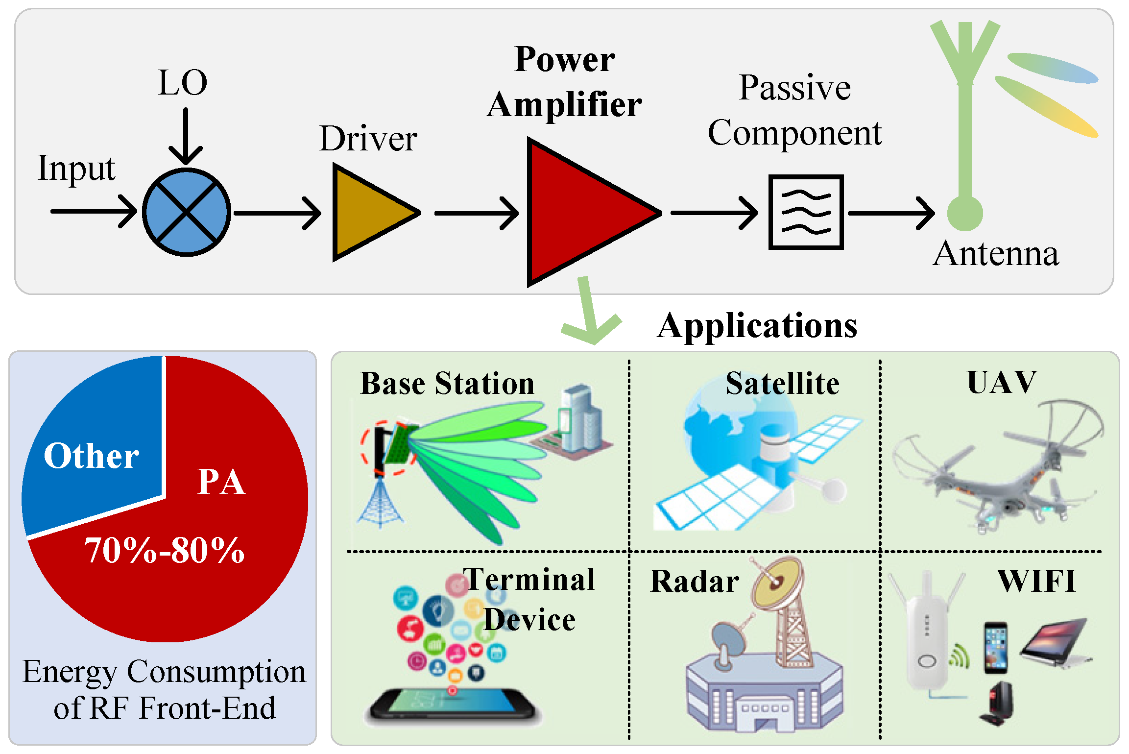
1. Introduction
2. Review on Doherty Power Amplifier
2.1. Introduction on Doherty Power Amplifier
2.2. Load Mismatch Compensation of Doherty Power Amplifier
3. Load-Modulated Balanced Amplifier
3.1. Introduction on LMBA
3.2. Load Mismatch Compensation of LMBA
4. Potential Solutions
5. Conclusions
Author Contributions
Funding
Conflicts of Interest
References
- Wang, A.; Feng, Z.; Li, X.; Pan, Y. Mine intelligent receiver: MIMO-OFDM intelligent receiver for mine information recovery. Energies 2022, 15, 6550. [Google Scholar] [CrossRef]
- Dbouk, T.; Mourad, O. A review on thermal management and heat dissipation strategies for 5G and 6G base stations: Challenges and solutions. Energies 2025, 18, 1355. [Google Scholar] [CrossRef]
- Wang, C.X.; You, X.; Gao, X.; Zhu, X.; Li, Z.; Zhang, C.; Wang, H.; Huang, Y.; Chen, Y.; Haas, H.; et al. On the road to 6G: Visions, requirements, key technologies, and testbeds. IEEE Commun. Surv. Tutorials 2023, 25, 905–974. [Google Scholar] [CrossRef]
- Femenias, G.; Riera-Palou, F. Wideband cell-free mmWave massive MIMO-OFDM: Beam squint-aware channel covariance-based hybrid beamforming. IEEE Trans. Wirel. Commun. 2022, 21, 4695–4710. [Google Scholar] [CrossRef]
- Jee, J.; Kwon, G.; Park, H. Joint precoding and power allocation for multiuser MIMO system with nonlinear power amplifiers. IEEE Trans. Veh. Technol. 2021, 70, 8883–8897. [Google Scholar] [CrossRef]
- Kang, H.; Lee, W.; Oh, S.; Oh, H.; Choi, W.; Lee, H.; Hwang, K.C.; Lee, K.Y.; Yang, Y. Optimized broadband load network for Doherty power amplifier based on bandwidth balancing. IEEE Microw. Wirel. Compon. Lett. 2021, 31, 280–283. [Google Scholar] [CrossRef]
- Hu, Y.; Gan, D.; Shi, W. Design of broadband Doherty power amplifier based on misaligned current phase. Energies 2024, 17, 2006. [Google Scholar] [CrossRef]
- Shi, W.; He, S.; Zhu, X.; Song, B.; Zhu, Z.; Naah, G.; Zhang, M. Broadband continuous-mode Doherty power amplifiers with noninfinity peaking impedance. IEEE Trans. Microw. Theory Tech. 2018, 66, 1034–1046. [Google Scholar] [CrossRef]
- Piacibello, A.; Camarchia, V.; Colantonio, P.; Giofre, R. 3-Way Doherty power amplifiers: Design guidelines and MMIC implementation at 28 GHz. IEEE Trans. Microw. Theory Tech. 2023, 71, 2016–2028. [Google Scholar] [CrossRef]
- Wang, W.; Chen, S.; Tang, Y.; Cai, J.; Crupi, G.; Xue, Q. Generalized theory and design methodology of broadband Outphasing power amplifiers employing low-order bandpass networks. IEEE Trans. Microw. Theory Tech. 2024, 72, 4611–4624. [Google Scholar] [CrossRef]
- Hu, C.; Yang, R.; Shi, W.; Li, L.; Gao, R.; Dai, Z.; Pang, J.; Li, M. Analysis and design of broadband Outphasing power amplifier based on complex combining impedance. IEEE Trans. Circuits Syst. I Reg. Papers 2023, 70, 1542–1554. [Google Scholar] [CrossRef]
- Cao, Y.; Lyu, H.; Chen, K. Asymmetrical load modulated balanced amplifier with continuum of modulation ratio and dual-octave bandwidth. IEEE Trans. Microw. Theory Tech. 2021, 69, 682–696. [Google Scholar] [CrossRef]
- Saad, P.; Hou, R. Symmetrical load modulated balanced power amplifier with asymmetrical output coupling for load modulation continuum. IEEE Trans. Microw. Theory Tech. 2022, 70, 2315–2327. [Google Scholar] [CrossRef]
- Belchior, C.; Nunes, L.C.; Cabral, P.M.; Pedro, J.C. Sequential LMBA design technique for improved bandwidth considering the balanced amplifiers off-state impedance. IEEE Trans. Microw. Theory Tech. 2023, 71, 3629–3643. [Google Scholar] [CrossRef]
- Gong, P.; Guo, J.; Vangipurapu, N.B.; Chen, K. Decade-bandwidth RF-input pseudo-Doherty load-modulated balanced amplifier using signal-flow-based phase alignment design. IEEE Microw. Wirel. Compon. Lett. 2024, 34, 761–764. [Google Scholar] [CrossRef]
- Yoon, Y.; Kim, H.; Kim, H.; Lee, K.S.; Lee, C.H.; Kenney, J.S. A 2.4-GHz CMOS power amplifier with an integrated antenna impedance mismatch correction system. IEEE J.-Solid-State Circuits 2014, 49, 608–621. [Google Scholar] [CrossRef]
- Kousai, S.; Onizuka, K.; Wadatsumi, J.; Yamaguchi, T.; Kuriyama, Y.; Nagaoka, M. Polar antenna impedance detection and tuning for efficiency improvement in a 3G/4G CMOS power amplifier. IEEE J.-Solid-State Circuits 2014, 49, 2902–2914. [Google Scholar] [CrossRef]
- Ji, D.; Jeon, J.; Kim, J. A novel load mismatch detection and correction technique for 3G/4G load insensitive power amplifier application. IEEE Trans. Microw. Theory Tech. 2015, 63, 1530–1543. [Google Scholar] [CrossRef]
- Donahue, D.T.; de Falco, P.E.; Barton, T.W. Power amplifier with load impedance sensing incorporated into the output matching network. IEEE Trans. Circuits Syst. I Reg. Papers 2020, 67, 5113–5124. [Google Scholar] [CrossRef]
- Paul, R.; Sankey, L.; Corradini, L.; Popovic, Z.; Maksimovic, D. Power management of wideband code division multiple access RF power amplifiers with antenna mismatch. IEEE Trans. Power Electron. 2010, 25, 981–991. [Google Scholar] [CrossRef]
- Gonçalves, C.F.; Barradas, F.M.; Nunes, L.C.; Cabral, P.M.; Pedro, J.C. Dynamic supply voltage control for PA output power correction under variable loading scenarios. IEEE Trans. Microw. Theory Tech. 2021, 69, 745–755. [Google Scholar] [CrossRef]
- Wan, Z.; Zhu, J.; Dai, L. Can continuous aperture MIMO obtain more mutual information than discrete MIMO. IEEE Commun. Lett. 2023, 27, 3185–3189. [Google Scholar] [CrossRef]
- Barradas, F.M.; Tome, P.M.; Gomes, J.M.; Cunha, T.R.; Cabral, P.M.; Pedro, J.C. Power, linearity, and efficiency prediction for MIMO arrays with antenna coupling. IEEE Trans. Microw. Theory Tech. 2017, 65, 5284–5297. [Google Scholar] [CrossRef]
- Xue, B.; Koivumäki, P.; Vähä-Savo, L.; Haneda, K.; Icheln, C. Impacts of real hands on 5G millimeter-wave cellphone antennas: Measurements and electromagnetic models. IEEE Trans. Instrum. Meas. 2023, 72, 1–12. [Google Scholar] [CrossRef]
- Imai, S.; Sato, H.; Mukai, K.; Okabe, H. A load-variation tolerant Doherty power amplifier with dual-adaptive-bias scheme for 5G handsets. In Proceedings of the IEEE International Solid-State Circuits Conference (ISSCC), San Francisco, CA, USA, 18–22 February 2024; pp. 524–526. [Google Scholar]
- Gashi, B.; Krause, S.; Quay, R.; Fager, C.; Ambacher, O. Investigations of active antenna Doherty power amplifier modules under beam-steering mismatch. IEEE Microw. Wirel. Compon. Lett. 2018, 28, 930–932. [Google Scholar] [CrossRef]
- Fager, C.; Eriksson, T.; Barradas, F.; Hausmair, K.; Cunha, T.; Pedro, J.C. Linearity and efficiency in 5G transmitters: New techniques for analyzing efficiency, linearity, and linearization in a 5G active antenna transmitter context. IEEE Microw. Mag. 2019, 20, 35–49. [Google Scholar] [CrossRef]
- Doherty, W.H. A new high efficiency power amplifier for modulated waves. Proc. Inst. Radio Eng. 1936, 24, 1163–1182. [Google Scholar]
- Shi, W.; Shi, W.; Peng, J.; Feng, L.; Gao, Y.; He, S.; Yue, C.P. Design and Analysis of Continuous-Mode Doherty Power Amplifier With Second Harmonic Control. IEEE Trans. Circuits Syst. II Express Briefs 2021, 68, 2247–2251. [Google Scholar] [CrossRef]
- Jia, S.; Chen, W.; Schreurs, D. A novel Doherty transmitter based on antenna active load modulation. IEEE Microw. Wirel. Compon. Lett. 2015, 25, 271–273. [Google Scholar] [CrossRef]
- Zhao, Y.L.; Ghannouchi, F.M.; Helaoui, M.; Li, X.; Du, X.; Zhang, W.; Apperley, T. Doherty transmitter based on monopole array antenna active load modulation. IEEE Microw. Wirel. Compon. Lett. 2018, 28, 927–929. [Google Scholar] [CrossRef]
- Li, S.; Chi, T.; Park, J.S.; Nguyen, H.T.; Wang, H. A 28-GHz flip-chip packaged Chireix transmitter with on-antenna outphasing active load modulation. IEEE J.-Solid-State Circuits 2019, 54, 1243–1253. [Google Scholar] [CrossRef]
- Chappidi, C.R.; Sharma, T.; Sengupta, K. Multi-port active load pulling for mm-Wave 5G power amplifiers: Bandwidth, back-off efficiency, and VSWR tolerance. IEEE Trans. Microw. Theory Tech. 2020, 68, 2998–3016. [Google Scholar] [CrossRef]
- Gonçalves, C.F.; Barradas, F.M.; Nunes, L.C.; Cabral, P.M.; Pedro, J.C. Quasi-load insensitive Doherty PA using supply voltage and input excitation adaptation. IEEE Trans. Microw. Theory Tech. 2022, 70, 779–789. [Google Scholar] [CrossRef]
- Singh, G.D.; Nemati, H.M.; Alavi, M.S.; de Vreede, L.C.N. An inverted Doherty power amplifier insensitive to load variation with an embedded impedance sensor in its output power-combining network. IEEE Trans. Microw. Theory Tech. 2023, 71, 5194–5208. [Google Scholar] [CrossRef]
- Imai, S.; Mukai, K.; Okabe, H.; Wada, T. Dual-adaptive bias scheme of condition-tolerant Doherty power amplifier for 5G handsets. IEEE Trans. Microw. Theory Tech. 2024; early access. [Google Scholar] [CrossRef]
- Guo, J.; He, S.; Yin, Y.; Liu, P.; Xiao, Z.; Zhang, X.; Zhong, T.; You, F. An ultra-broadband load-insensitive dual-input Doherty power amplifier MMIC using configurable supply voltage for 5G smartphones. IEEE Trans. Microw. Theory Tech. 2024; early access. [Google Scholar] [CrossRef]
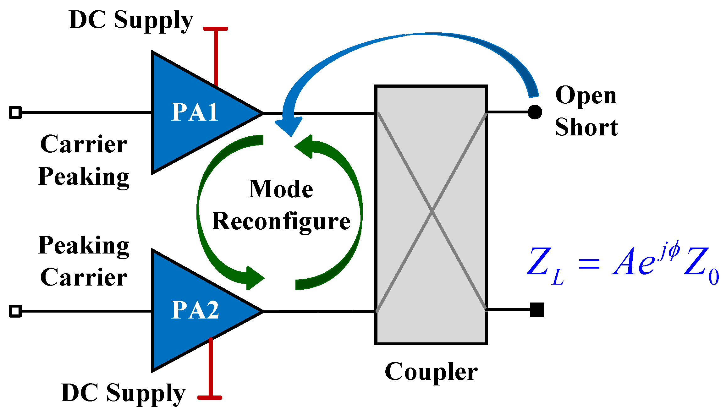
- Shi, W.; Li, X.; Gao, Y.; Hu, C.; Dai, Z.; Pang, J.; Li, M. Load mismatch compensation of Doherty power amplifier using dual-input and mode reconfiguration techniques. IEEE Trans. Circuits Syst. I Reg. Papers 2023, 70, 2774–2787. [Google Scholar] [CrossRef]
- Lyu, H.; Chen, K. Balanced-to-Doherty mode-reconfigurable power amplifier with high efficiency and linearity against load mismatch. IEEE Trans. Microw. Theory Techn. 2020, 68, 1717–1728. [Google Scholar] [CrossRef]
- Mannem, N.S.; Huang, M.Y.; Huang, T.Y.; Wang, H. A reconfigurable hybrid series/parallel Doherty power amplifier with antenna VSWR resilient performance for MIMO arrays. IEEE J.-Solid-State Circuits 2020, 55, 3335–3348. [Google Scholar] [CrossRef]
- Lyu, H.; Cao, Y.; Chen, K. Linearity-enhanced quasi-balanced Doherty power amplifier with mismatch resilience through series/parallel reconfiguration for massive MIMO. IEEE Trans. Microw. Theory Tech. 2021, 69, 2319–2335. [Google Scholar] [CrossRef]
- Lyu, H.; Chen, K. Analysis and design of reconfigurable multiband mismatch-resilient quasi-balanced Doherty power amplifier for massive MIMO systems. IEEE Trans. Microw. Theory Tech. 2022, 70, 4410–4421. [Google Scholar] [CrossRef]
- Pang, J.; Han, Y.; Peng, J.; Li, M.; Dai, Z.; Shi, W.; Zhou, X.; Zhu, A. Dual-mode three-way Doherty power amplifier with extended high-efficiency range against load mismatch. IEEE Trans. Microw. Theory Tech. 2024, 72, 4058–4067. [Google Scholar] [CrossRef]
- Shepphard, D.J.; Powell, J.; Cripps, S.C. An efficient broadband reconfigurable power amplifier using active load modulation. IEEE Microw. Wirel. Compon. Lett. 2016, 26, 443–445. [Google Scholar] [CrossRef]
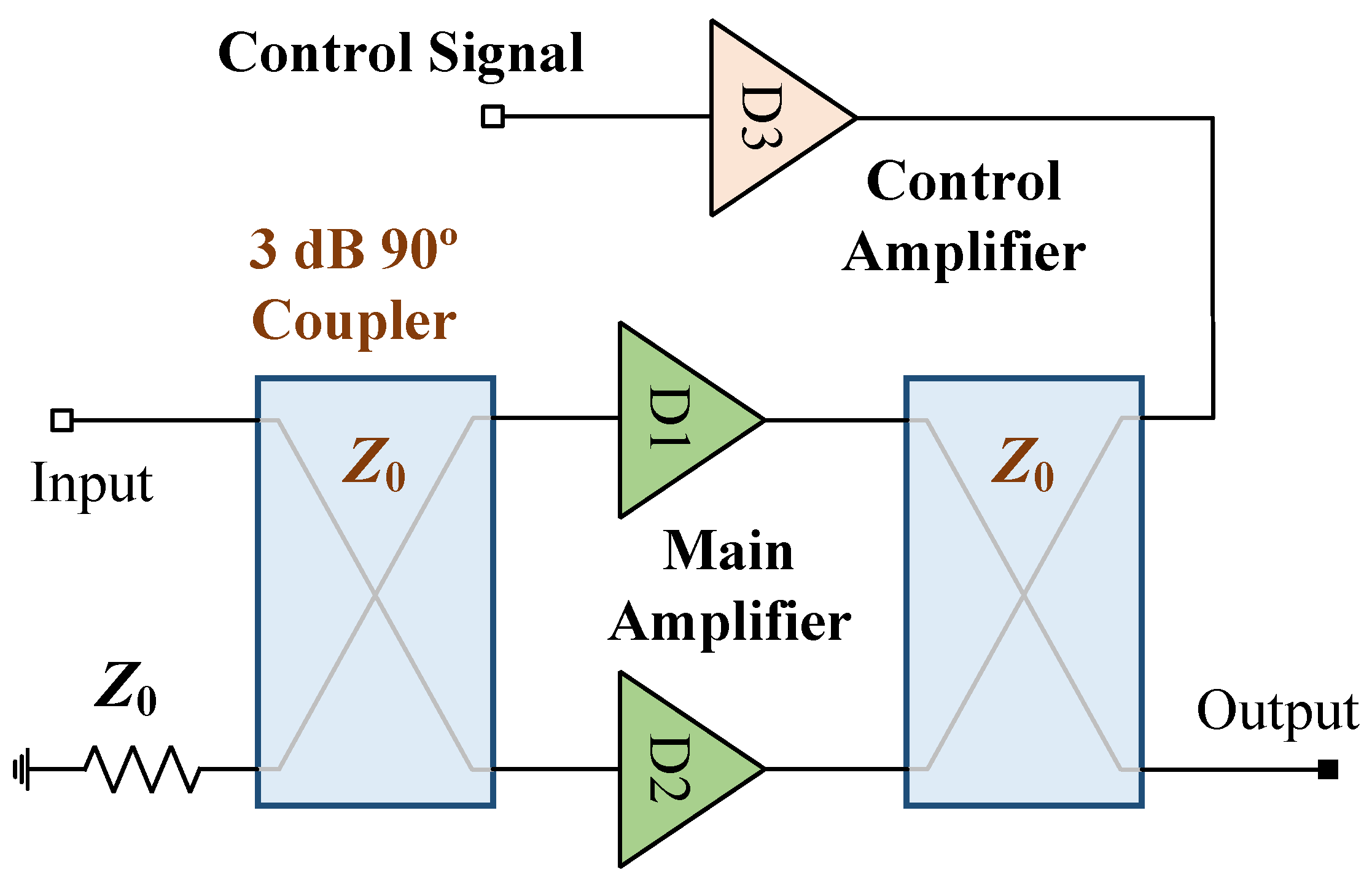
- Pednekar, P.H.; Berry, E.; Barton, T.W. RF-input load modulated balanced amplifier with octave bandwidth. IEEE Trans. Microw. Theory Tech. 2017, 65, 5181–5191. [Google Scholar] [CrossRef]
- Cao, Y.; Chen, K. Pseudo-Doherty load-modulated balanced amplifier with wide bandwidth and extended power back-off range. IEEE Trans. Microw. Theory Tech. 2020, 68, 3172–3183. [Google Scholar] [CrossRef]
- Pang, J.; Li, Y.; Li, M.; Zhang, Y.; Zhou, X.Y.; Dai, Z.; Zhu, A. Analysis and design of highly efficient wideband RF-input sequential load modulated balanced power amplifier. IEEE Trans. Microw. Theory Tech. 2020, 68, 1741–1753. [Google Scholar] [CrossRef]
- Cao, Y.; Lyu, H.; Chen, K. Continuous-mode hybrid asymmetrical load-modulated balanced amplifier with three-way modulation and multi-band reconfigurability. IEEE Trans. Circuits Syst. I Reg. Papers 2022, 69, 1077–1090. [Google Scholar] [CrossRef]
- Yang, R.; Shi, W.; Hu, C.; Lin, S.; Dai, Z.; Pang, J.; Li, M. Asymmetrical sequential load modulated balanced amplifier with composited impedance inverter and reciprocal mode for broadband applications. IEEE Trans. Circuits Syst. II Express Briefs 2023, 70, 4374–4378. [Google Scholar] [CrossRef]
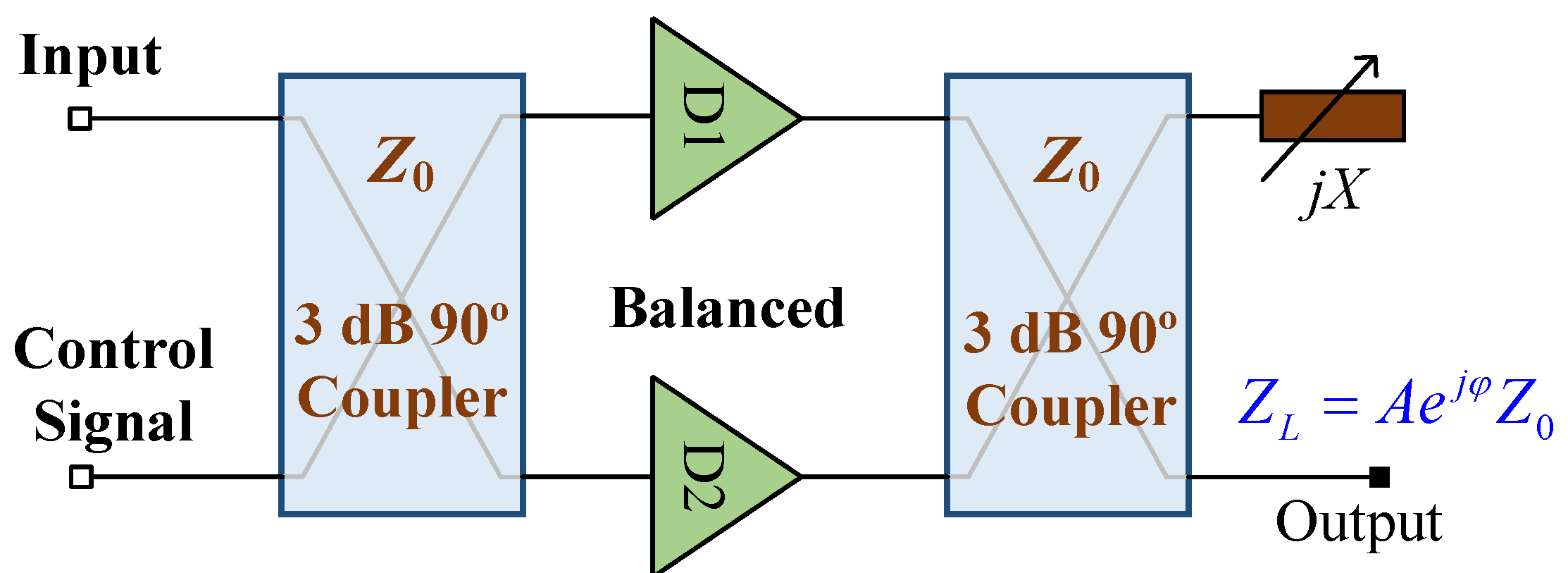
- Quaglia, R.; Powell, J.R.; Chaudhry, K.A.; Cripps, S.C. Mitigation of load mismatch effects using an orthogonal load modulated balanced amplifier. IEEE Trans. Microw. Theory Tech. 2022, 70, 3329–3341. [Google Scholar] [CrossRef]
- Guo, J.; Cao, Y.; Chen, K. 1-D reconfigurable pseudo-Doherty load modulated balanced amplifier with intrinsic VSWR resilience across wide bandwidth. IEEE Trans. Microw. Theory Tech. 2023, 71, 2465–2478. [Google Scholar] [CrossRef]
- Guo, J.; Cao, Y.; Chen, K. Linear hybrid asymmetrical load-modulated balanced amplifier with multiband reconfigurability and antenna-VSWR resilience. IEEE Trans. Microw. Theory Tech. 2024, 72, 5319–5332. [Google Scholar] [CrossRef]
- Guo, J.; Chen, K. Load-modulated double-balanced amplifier with quasi-isolation to load. In Proceedings of the IEEE Wireless and Microwave Technology Conference (WAMICON), Melbourne, FL, USA, 17–18 April 2023; pp. 144–147. [Google Scholar]


| Ref. | Architecture | Frequency (GHz) | Mismacth | Power (dBm) | (%) | (%) | Technique |
|---|---|---|---|---|---|---|---|
| [34] | Symmetrical DPA | 3.6 | 2:1 VSWR | 42.6–43.8 | 49–63 | 35–50@6dB | Input Tuning; Supply Tuning |
| [35] | Symmetrical DPA | 0.9 | 2:1 VSWR | 30.7–31.1 | 57.8–67.2 | N/A | Supply Tuning |
| [38] | Symmetrical DPA | 2.4 | 2:1 VSWR | 42.4–44.3 | 54.2–66.7 | 50.7–62.5@6dB | Mode Reconfiguration |
| [41] | Symmetrical DPA | 3.5 | 2.5:1 VSWR | 38.8–40.4 | 50–60 * | 33–43@6dB * | Mode Reconfiguration |
| [42] | Symmetrical DPA | 1.7–2.7 | 2:1 VSWR | 39.1–40.2 | 49–62 | 38.1–42.9@6dB | Mode Reconfiguration |
| [43] | Three-way DPA | 2.0 | 2:1 VSWR | 44.8–46.3 | 50.2–65.8 | 47.8–56.7@9dB | Mode Reconfiguration |
| [51] | PD-LMBA | 1.7–2.9 | 2:1 VSWR | 39.1–41.4 | 51.9–72.8 | 38.6–65.4@10dB | Supply Tuning |
| [52] | HALMBA | 1.7–2.9 | 2:1 VSWR | 40–42.9 | 47.1–64.8 | 43.8–57.2@10dB | Mode Reconfiguration |
Disclaimer/Publisher’s Note: The statements, opinions and data contained in all publications are solely those of the individual author(s) and contributor(s) and not of MDPI and/or the editor(s). MDPI and/or the editor(s) disclaim responsibility for any injury to people or property resulting from any ideas, methods, instructions or products referred to in the content. |
© 2025 by the authors. Licensee MDPI, Basel, Switzerland. This article is an open access article distributed under the terms and conditions of the Creative Commons Attribution (CC BY) license (https://creativecommons.org/licenses/by/4.0/).
Share and Cite
Zang, Y.; Shi, W.; Liu, J.; Qi, T.; Li, M. Load Mismatch Compensation of Load-Modulated Power Amplifiers: A Comprehensive Review. Energies 2025, 18, 2157. https://doi.org/10.3390/en18092157
Zang Y, Shi W, Liu J, Qi T, Li M. Load Mismatch Compensation of Load-Modulated Power Amplifiers: A Comprehensive Review. Energies. 2025; 18(9):2157. https://doi.org/10.3390/en18092157
Chicago/Turabian StyleZang, Yufeng, Weimin Shi, Jinting Liu, Tian Qi, and Mingyu Li. 2025. "Load Mismatch Compensation of Load-Modulated Power Amplifiers: A Comprehensive Review" Energies 18, no. 9: 2157. https://doi.org/10.3390/en18092157
APA StyleZang, Y., Shi, W., Liu, J., Qi, T., & Li, M. (2025). Load Mismatch Compensation of Load-Modulated Power Amplifiers: A Comprehensive Review. Energies, 18(9), 2157. https://doi.org/10.3390/en18092157