1. Introduction
Due to the environmental and energy crises, more and more researchers are paying attention to novel energy vehicles, such as electric vehicles (EVs) and hybrid electric vehicles (HEVs). It is widely known that battery chargers play a critical role in the development of EVs, and the charging time and lifetime of batteries are closely related to the characteristics of the chargers. A battery charger must be efficient and reliable, with low cost, low volume and low weight, as well as high-power output capability [
1,
2,
3,
4,
5]. Most of the chargers can be divided into two types: onboard chargers (OBCs) and off-board chargers (FBCs). Generally, FBCs are located in charging station, which are suitable for fast charging. However, the expensive construction cost and limited locations (mostly in big cities) have limited the wide application of FBCs. Different from FBCs, OBCs mean taking the chargers with the vehicles and thus having relatively higher flexibility, which makes it possible to get charged through a socket. Thereby, the OBCs are supposed to be a better alternative for customers. However, OBCs have some specific limitations, since the added charger will increase the volume, weight and cost, as well as the charging time, which is too long for normal usage. Therefore, novel OBCs with low volume, high efficiency, high power density and high power capability are needed [
3].
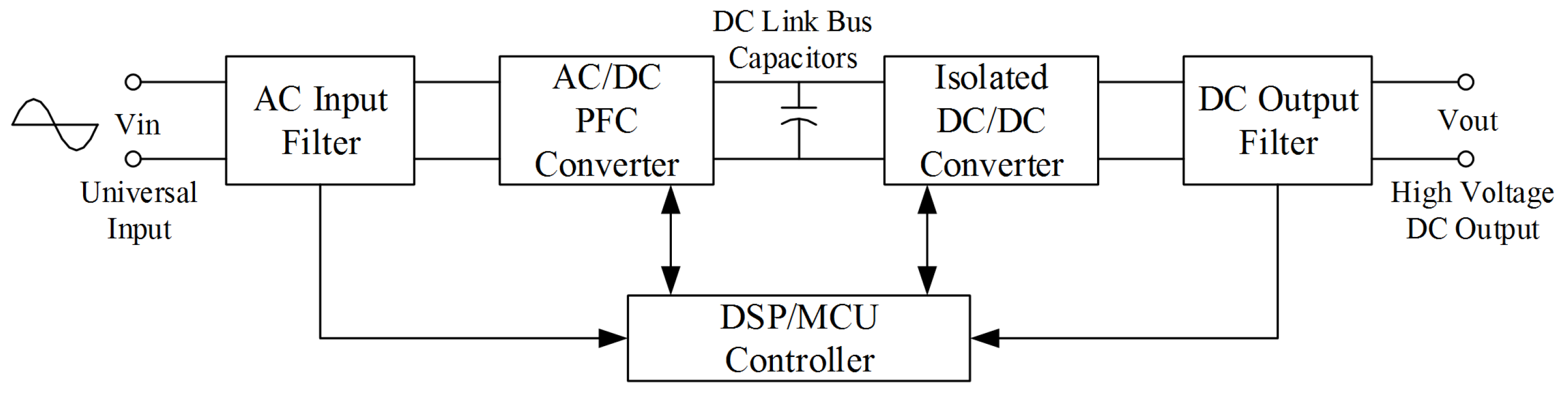
From the perspective of structure, OBCs are classified into two types: a single-stage topology and a multi-stage topology. The multi-stage (mostly two-stage) structures are commonly used at present due to their favorable features. A simplified structure of the two-stage OBC using digital signal processor (DSP) or microcontroller unit (MCU) as controller is shown in
Figure 1. The two-stage structure has the advantages of a wide adjustable output voltage range and high flexibility of the output load. To satisfy the requirements of the conversion efficiency, soft switching technology is widely used in the DC/DC converter. The most commonly-used topologies are the phase shifted zero-voltage-switching (ZVS) topology [
6,
7,
8,
9,
10] and the resonant tank with two inductors and a capacitor (LLC) resonant topology [
11,
12,
13]. The shifted ZVS topology can achieve a relatively high output power level, which is more than a dozen kilowatts with an efficiency between 95% and 97%. However, it also has some drawbacks, such as a limited soft switching range and being sensitive to the parasitic parameters of switch devices and the leakage inductance of the transformer. All of these problems will increase the design difficulty. The LLC resonant topology has disadvantages, such as a low power rating and a rigorous design of the transformer and inductor because of the parasitic parameters. In addition, the wide frequency range of the LLC structure increases the difficulty of the design process for the input electromagnetic interference (EMI) filter.
Figure 1.
Simplified block diagram of a universal single-phase onboard charger (OBC); power factor correction (PFC).
Figure 1.
Simplified block diagram of a universal single-phase onboard charger (OBC); power factor correction (PFC).
Compared with the two-stage structure, the single-stage structure will reduce the number of devices and circuit complexity, so it is easier to get low volume, high efficiency and high power density. Furthermore, to realize rapid charging for EVs, three-phase AC/DC converters are widely used in the single-stage charging structure.
A large number of three-phase AC-DC converters have been developed to improve power factor correction (PFC), to reduce THD and EMI of the AC input and to regulate DC output, which are addressed as the three-phase improved power quality AC-DC converters (IPQCs). Concerning topologies, these circuits can be classified into five categories: buck, boost, buck-boost, multilevel and multi-pulse [
14].
The output voltage of the boost IPQCs is higher than the peak input voltage, which will result in a high output voltage or a decrease of the input voltage to satisfy the output requirement. Therefore, this kind of converter is usually used to provide a constant, regulated DC output voltage [
14,
15]
. Furthermore, there are many problems hindering the buck-boost IPQCs from high-power applications, such as the storage capacitor selection and the reversed output voltage polarity. Therefore, the boost and buck-boost IPQCs are not suitable for the single-stage OBC application.
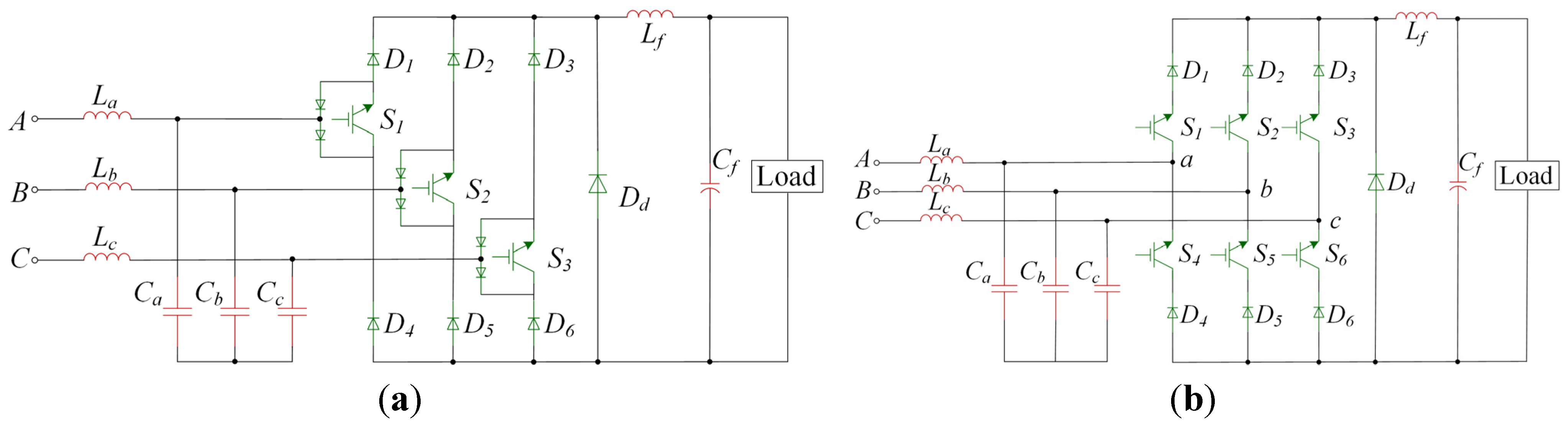
The buck IPQCs with high-frequency switching devices are extensively used in battery charging for automotive applications [
16]. These circuits can reduce the filter size and weight and enhance the efficiency of the system. Several topologies, such as using a single switch with a diode bridge rectifier [
17], three switches with a dual diode, shown in
Figure 2a [
18], and six switches with free-wheeling diodes, shown in
Figure 2b [
19], are used to improve the power factor, to reduce the harmonic currents of AC input and to get a well-filtered output DC voltage.
Figure 2.
Three-phase AC-DC buck converters: (a) three-switch buck converter; (b) six switch with free-wheeling diode buck converter.
Figure 2.
Three-phase AC-DC buck converters: (a) three-switch buck converter; (b) six switch with free-wheeling diode buck converter.
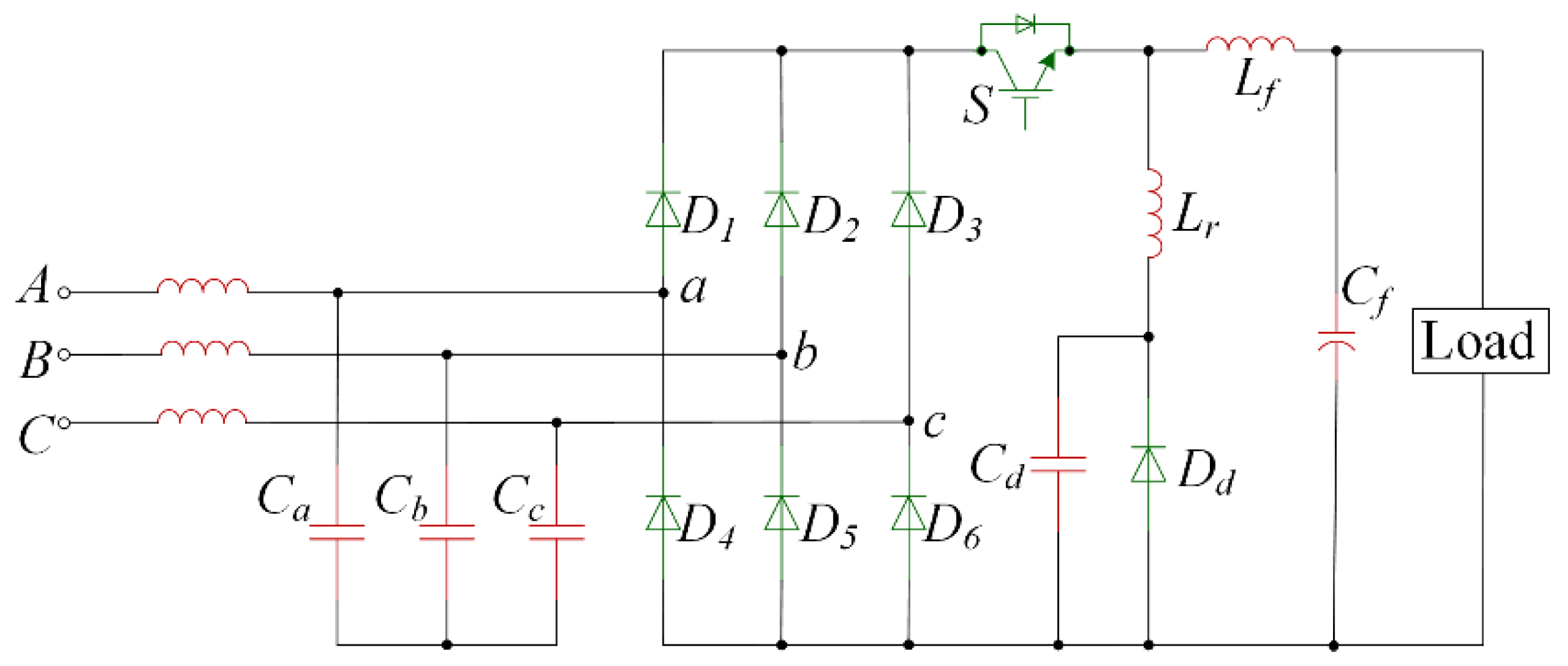
To enhance the efficiency and switching frequency of buck IPQCs, Robert W. Erickson and Yungtaek Jang proposed a new zero-current-switching (ZCS) three-phase high quality rectifier, which is illustrated in
Figure 3 [
15,
20,
21]. In this three-phase ZCS buck circuit, continuous input and output currents, a high power factor and low harmonic rectification are achieved. By the usage of a multi-resonant scheme, the switch operates in ZCS mode, and the diodes operate in ZVS mode; therefore, this circuit is suitable for the high-frequency implementation with insulated gate bipolar transistor (IGBT) [
21].
Figure 3.
New three-phase multi-resonant zero-current-switching buck rectifier.
Figure 3.
New three-phase multi-resonant zero-current-switching buck rectifier.
In view of the aforementioned advantages, this three-phase ZCS buck topology is adopted and optimized in this article. Although this topology can satisfy the requirement of single-stage OBC in general, the battery characteristics and the ZCS boundary condition of the multi-resonant tank, as well as their influence on each other have to be considered. Moreover, the output voltage and current fluctuations should be carefully considered for different battery statuses. Many charging strategies for EV batteries have been proposed [
22,
23,
24,
25,
26]. Comprehensively considering the life cycle of batteries and the feasibility of the control methods, the three-stage charging strategy is selected in this article. Then, this article studies the influence between the realization of ZCS and the battery parameters or status changes and solves the problem of the large input current ripple and the useless large resonant current within the tank when the driving frequency is extremely low under light load conditions.
In addition, an interleaved structure is used to improve the power level of the OBC system in this paper, which can reduce the charging current ripple and inductor size, and it also reduces the current stress on output capacitors [
1,
27,
28]. Finally, a prototype platform was built to verify the feasibility of the proposed topology. Besides, the SiC Schottky diodes were applied to promote the power level and the system efficiency [
29,
30].
The structure of this article is organized as follows. The operating states and principles are shown in
Section 2.
Section 3 explains the process of the system design, the ZCS border conditions, the impact caused by the battery load and the novel PWM and PFM combined control strategy.
Section 4 presents the simulation and experimental results to evaluate the proposed converter. Finally,
Section 5 concludes the work carried out in this article.
2. System Introduction
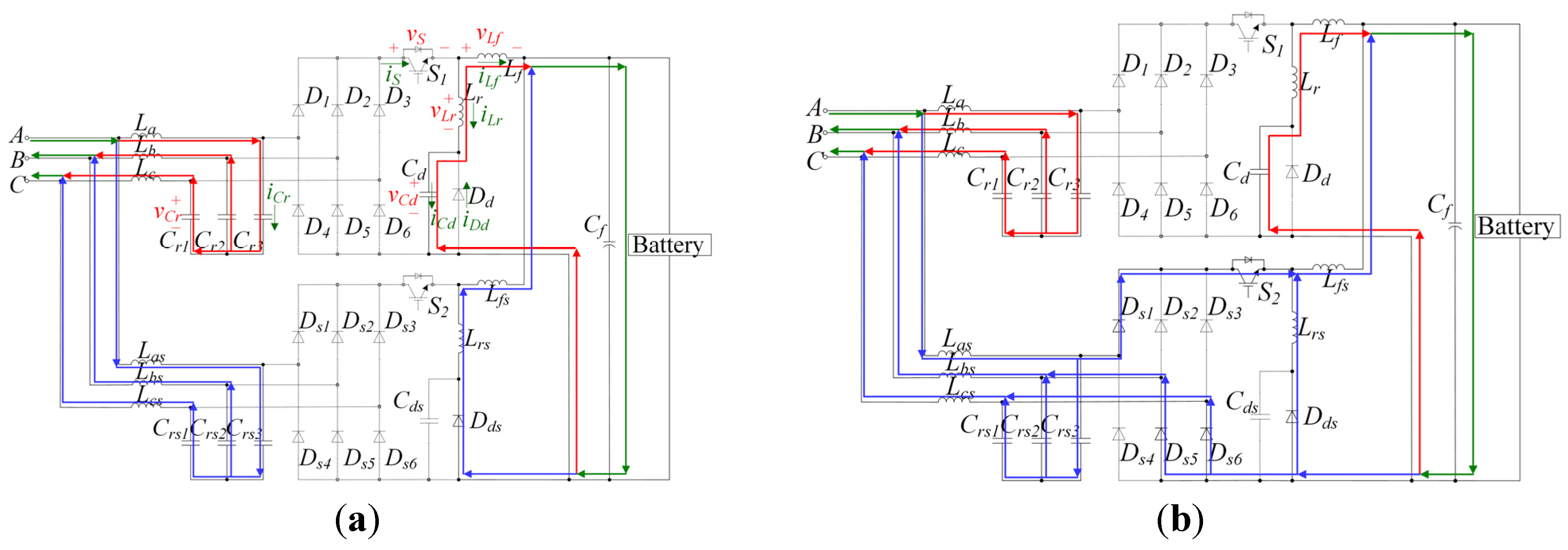
The proposed interleaved three-phase multi-resonant ZCS OBC is shown in
Figure 4. It is composed of the input filter inductors
La,
Lb,
Lc,
Las,
Lbs,
Lcs, input resonant capacitors
Cr1,
Cr2,
Cr3,
Crs1,
Crs2,
Crs3, uncontrolled rectifier bridges
D1–
D6 and
Ds1–
Ds6, resonant inductors
Lr and
Lrs, output resonant capacitors
Cd and
Cds, fly-wheel diodes
Dd and
Dds, output filter inductor
Lf and
Lfs and output filter capacitor
Cf. In this topology,
Cr1–
Cr3,
Cd and
Lr constitute a resonant tank, and the resonance cycle of this is fixed. Therefore, the PFM control strategy with a constant turn on time is adopted, and the output voltage will increase with the driving frequency increasing while other circuit parameters remain the same.
Figure 4.
The proposed OBC.
Figure 4.
The proposed OBC.
Due to the structures of the two interleaved channels being completely the same, the following analysis is based on the single-channel structure. This topology is established on the basis of the three-phase single-switch rectifier [
16], in which the output voltage is controllable from zero to the peak AC input line voltage. Only one IGBT in each channel needs to be controlled in this structure. In the proposed topology,
Cr1–
Cr3,
Cd and
Lr constitute a multi-resonant tank, which can guarantee the IGBTs
S1 and
S2 working in ZCS mode and diodes
Dd and
Dds operating in ZVS mode. Moreover, by the usage of the multi-resonant scheme and the interleaved structure, this converter can improve the power level and achieve high quality input current and almost unity power factor; which can reduce the input and output side ripples and decrease the volume of the circuit.
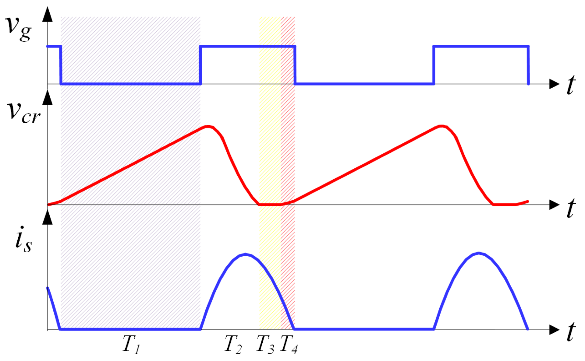
The operating waveforms of the input side resonant capacitor
vcr and IGBT current
is are shown in
Figure 5. The voltage
vcr can be divided into four parts: during
T1, IGBT is turned off, and
Cr is charged with input current; during
T2,
Cr ,
Lr and
Cd form a resonant tank, until
vcr decreases to zero;
vcr remains zero during
T3; during
T4,
Cr is charged with a current of input line current
iin minus the IGBT current
is. While the average value of
vcr is the same as the input voltage during each switching cycle, and peak value of
vcr is proportional to the input current. If interval
T1 is much longer than the sum of
T2,
T3 and
T4, the input current will follow the input voltage waveform. The details of the working process and control strategy will be analyzed below.
Figure 5.
The waveforms of the input side capacitor voltage vcr and insulated gate bipolar transistor (IGBT) currentis.
Figure 5.
The waveforms of the input side capacitor voltage vcr and insulated gate bipolar transistor (IGBT) currentis.
2.1. Operating States
Both of the interleaved channels adopt same control strategy, but hold a phase shift of π in driving signal from each other. Assuming that the three-phase input voltages are symmetrical and balanced, it is sufficient to consider a 30-degree interval of the AC input. The 30-degree interval where va > 0 > vc > vb is introduced. In order to simplify the algorithm, we choose the operating point at π/2 to analyze the operating process of each period.
VPM and IPM represent the peak input phase voltage and current, respectively. At the point of π/2, both vA and iA reach the peak value of the phase voltage and current, and vB = vC = −0.5vA, vA = VPM. Similarly, iB = iC= −0.5iA, iA = IPM. At this point, the input side resonant capacitor Cr2 and Cr3 are charged and discharged entirely synchronously, and diodes of phase B and C of the uncontrolled rectifier are turned on and off synchronously, too. Therefore, the following analysis of Cr3 is neglected.
Since the driving frequency is much higher than the input voltage frequency, so during one switching cycle the input voltage and current can be considered as a constant value. The ideal operating waveforms of the OBC is shown in
Figure 6, and the equivalent circuits of each interval are shown in
Figure 7.
Figure 6.
Ideal waveforms of the charger mode.
Figure 6.
Ideal waveforms of the charger mode.
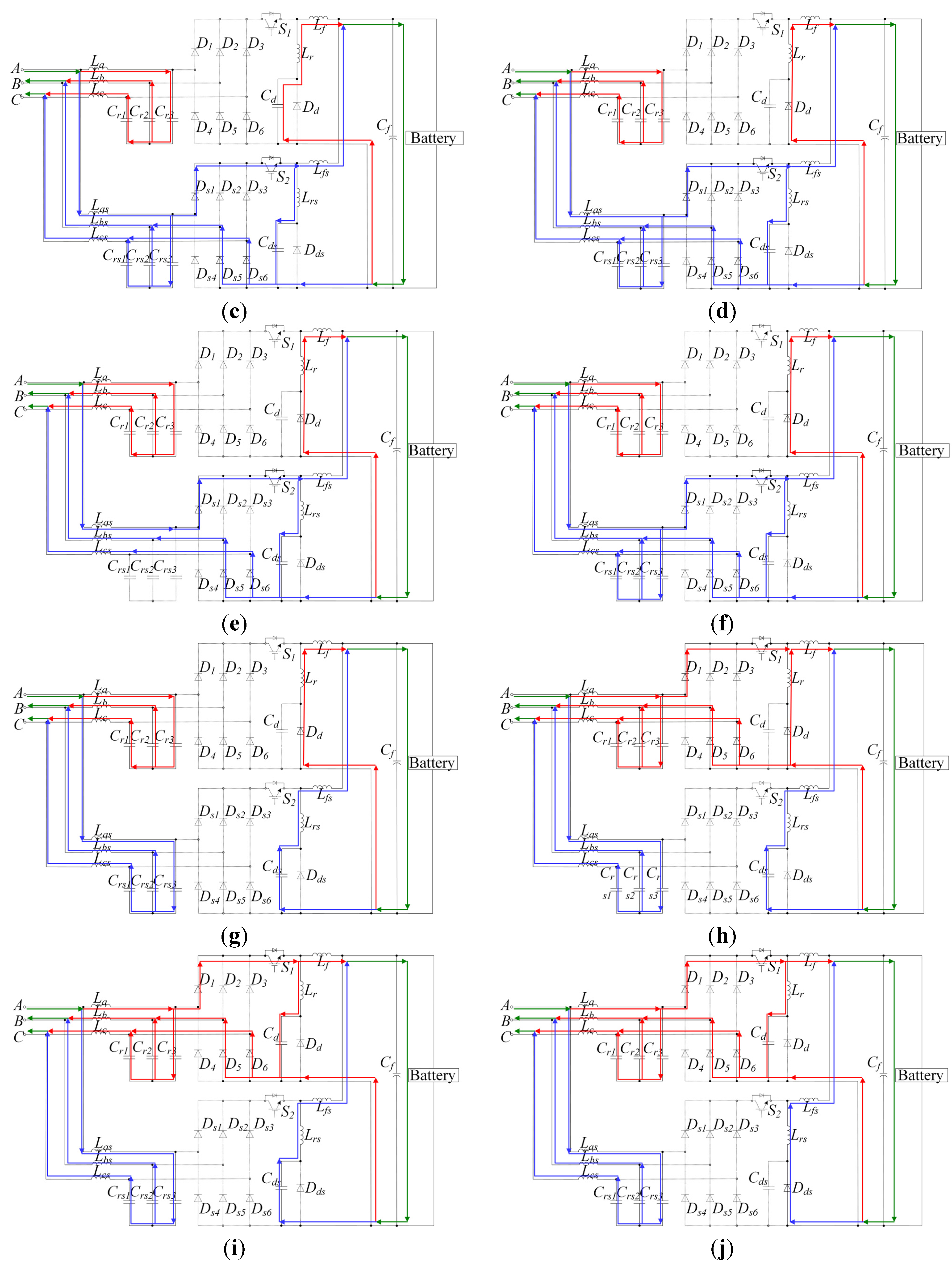
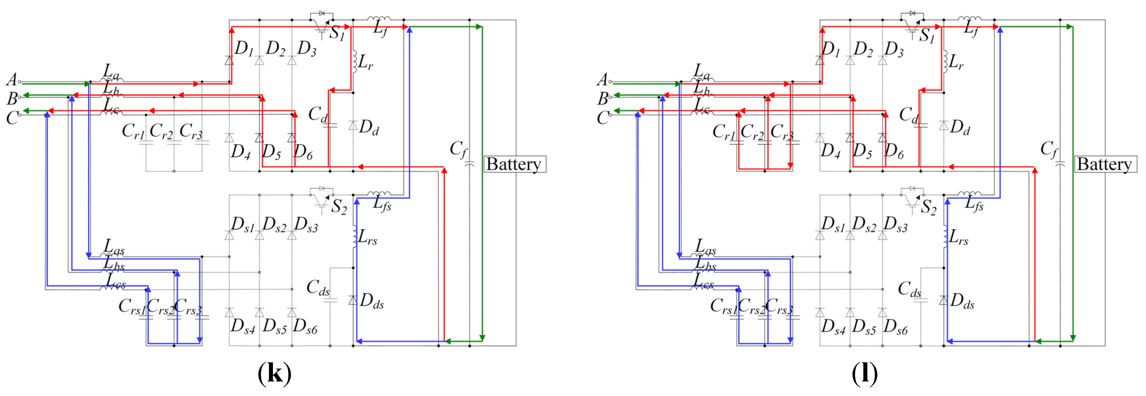
Figure 7.
Equivalent circuits of each interval. (a) t0–t1; (b) t1–t2; (c) t2–t3; (d) t3–t4; (e) t4–t5; (f) t5–t6; (g) t6–t7; (h) t7–t8; (i) t8–t9; (j) t9–t10; (k) t10–t11; (l) t11–t12.
Figure 7.
Equivalent circuits of each interval. (a) t0–t1; (b) t1–t2; (c) t2–t3; (d) t3–t4; (e) t4–t5; (f) t5–t6; (g) t6–t7; (h) t7–t8; (i) t8–t9; (j) t9–t10; (k) t10–t11; (l) t11–t12.
The parameters are defined as follows:
vCr1–vCr3 and
iCr1–iCr3 are the voltage and current of resonant capacitors
Cr1–Cr3, respectively;
vCd and
iCd are the voltage and current of the resonant capacitor
Cd, respectively;
vLr and
iLr are the voltage and current of the resonant inductor
Lr, respectively;
Iout is the output current;
Vout is the output voltage;
iCf is the current of
Cf. Since the two paralleled channels use the same control strategy, the single channel will be introduced in the following theoretical analysis and calculation parts. The input and output current for each channel are the half of the total circuit and can be defined as 0.5
IPM and 0.5
Iout. The capacitance values of
Cr1–Cr3 are the same and can be represented as
Cr.
Figure 7a illustrates the voltage and current reference directions of the devices for the following analysis, and the reference directions of
Cr1–Cr3 are exactly the same.
Interval I (
t0–t3):
D1–D6,
S1 and
Dd are off.
Cr1–Cr3 are charged by the input current. During this interval,
Lr provides the output current.
Cd is discharged with
iLr, and
Cf is also charged. This interval ends when
vCd decreases to zero and
Dd is turned on. The state equations of this interval are:
In Equation (1), i(t) represents the fluctuation component of the freewheel current through Cd, Lr and Lf. From the perspective of the current analysis, i(t) can be ignored, while in the voltage analysis, i(t) will cause a decided change of VLf(t). Moreover, VLr(t) can be considered as a constant value in this interval, in view of the fact that compared to Lf, the value of Lr is very small.
Interval II (
t3 ~ t7):
Dd is on, and
D1 ~ D6 and
S1 are off. The output current is still supplied by
Lr. The only difference between Interval I and Interval II is that the current flows through
Dd, rather than the resonant capacitor
Cd. This interval ends when the switch
S1 is turned on. The state equations of this interval are:
Interval III (
t7–t8):
D1,
D5,
D6,
S1 and
Dd are on, and the other diodes are off.
Cr1–Cr3 and
Lr form a resonant tank, until the inductor current increases to zero. The state equations of this interval are:
Interval IV (
t8–t10):
D1,
D5,
D6 and
S1 are on, and
D2–D4 and
Dd are off.
Cd,
Cr and
Lr form a resonant tank. This interval ends until the voltage of
Cr decreases to zero. The state equations of this interval are:
Interval V (
t10–t11):
D1–D6 and
S1 are on, and
Dd is off.
Lr and
Cd form a resonant tank. This interval ends when the current
iS1 reduces to the input current 0.5
IPM. If
iS1 < 0.5
IPM, then the current
iCr1 > 0, and the input capacitor begins to charge, indicating that this interval ends. The state equations of this interval are:
Interval VI (
t11–t12):
D1,
D5,
D6 and
S1 are on, and
D2–D4 and
Dd are off.
Cr,
Cd and
Lr form a resonant tank. This interval ends when the current
iS1 decreases to zero. After this ending point,
S1 can realize turning on of ZCS. The state equations of this interval are:
2.2. Operating Analysis
This section will carry out a further analysis of the operating principle during each interval. From the state Equations (1)–(6), the current and voltage expressions of S1, Lr, Cr and Cd can be calculated. Then, the starting and ending point of each interval are confirmed, which will be used to determine the ZCS boundary and to provide the basis for the circuit design.
By solving Equation (1), the expressions of the main power devices of Interval I are listed as:
As analyzed above, Interval I will end when
vCd decreases to zero, so the ending moment
T1 and
C11 can be deduced as:
Then, the value of each electric parameter at the ending time of Interval I can be derived as:
Similarly, by solving Equations (2)–(6), the expressions of Intervals II–VI can be obtained.
For Interval II, the expressions of the main devices of can be listed as:
For the duration of Interval II,
T2 and the final value of each electric parameter can be inferred as:
For Interval III, the expressions of the main devices can be listed as:
By substituting the final value of Interval II into Equation (15), the parameters can be shown as:
For the duration of Interval III,
T3 and the final value of each parameter can be deduced as:
For Interval IV, the voltage and current expressions of the main devices can also be deduced by solving Equation (4). They can be listed as:
The parameters of Equation (20) can be determined by the final value of Interval III.
For the duration of Interval IV,
T4 and the final value of each electric parameter can be derived as:
For Interval V, according to the above operating states’ analysis, we can deduce the expressions of the electrical parameters as:
The parameters in Equation (25) are listed as:
Since this interval ends when
iS1 reduces to 0.5
IPM and from Equations (25)–(27), the time length of this interval
T5 can be deduced as:
Then, we can get the final value of each electric parameter as:
For Interval VI, we can deduce the expressions of the electrical parameters as:
From Equations (30)–(32), the time length of this interval
T6 is:
Then, we can get the final value of each parameter as:
3. System Design
In this section, based on the analysis above and the battery charging requirements, the hardware parameters and control strategy are designed. The design mainly focuses on the ZCS realization when considering the differences of battery parameters and charging conditions.
3.1. ZCS Condition Analysis
The system cannot realize ZCS under two conditions, which are:
- (1)
The circuit parameters do not satisfy the ZCS requirement.
- (2)
The circuit parameters are appropriate, but the driving signal is mismatched.
3.1.1. Mismatch of Circuit Parameters
To realize ZCS, the previous stage should provide the conditions to obtain the next stage. From the ideal waveforms in
Figure 6 and the operating analysis above, we can deduce the constraint expressions.
Interval I and II should be long enough to guarantee energy storage, for the resonant inductor current to be positive. This can be expressed as, at the end of Interval III, the voltage of
vCr is positive.
Cr must be completely discharged when the resonant inductor current is positive. This can be expressed as:
During Interval V and Interval VI,
Lr and
Cd form a resonant tank. Only if
Cd have enough energy, the resonant inductor current can reach output current 0.5
Iout, and
iS can reach zero to realize ZCS. It can be described as:
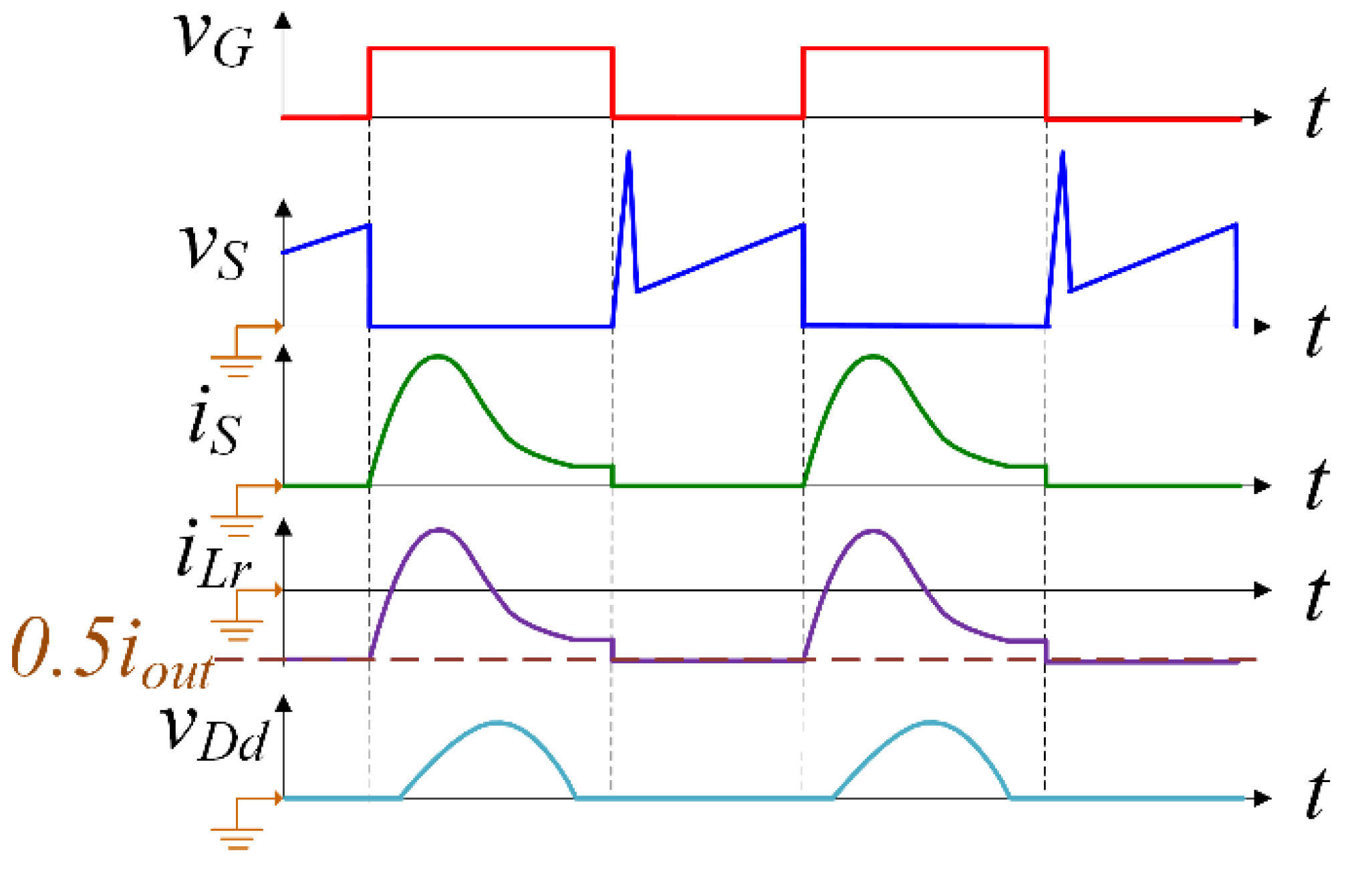
Figure 8 shows the working waveforms with mismatched circuit parameters, where the converter cannot realize ZCS. We can see that the output side resonant capacitor is entirely discharged before
iS decreases to zero. Thus,
iS fails to drop down to zero, and ZCS cannot be realized.
Figure 8.
Typical waveforms with mismatch circuit parameters.
Figure 8.
Typical waveforms with mismatch circuit parameters.
3.1.2. Mismatch of the Driving Signal
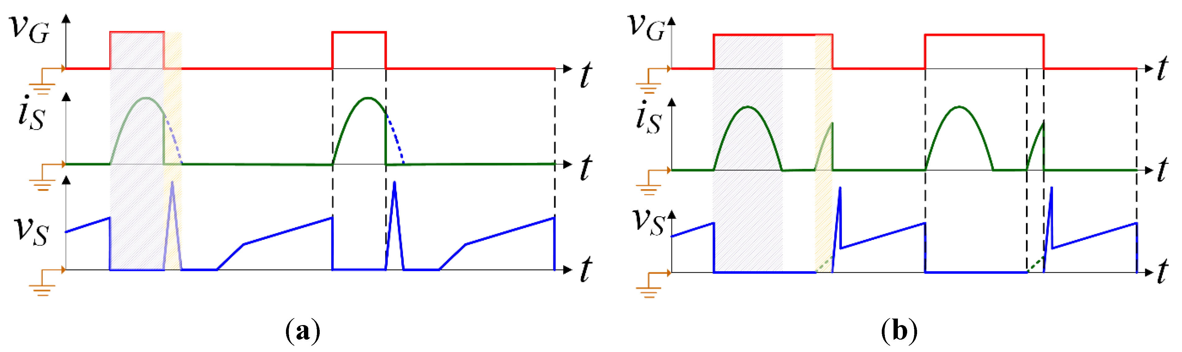
ZCS can only be realized when the circuit and the driving signal are matched. The condition that optimizes the circuit parameters with an improper driving signal is discussed below, and the typical waveforms are shown in
Figure 9.
Figure 9a shows the waveforms when
Ton is shorter than the minimum allowable value, and
Figure 9b shows the waveforms when
Ton is longer than the maximum allowable value.
Figure 9.
Theoretical waveforms with mismatch driving signal. (a) Ton is too short and (b) Ton is too long
Figure 9.
Theoretical waveforms with mismatch driving signal. (a) Ton is too short and (b) Ton is too long
Regarding the ideal waveforms of the proposed converter, which are shown in
Figure 6, ZCS can only be realized during a specified period. Additionally, if the drive signal turns to zero before
iS1 decreases to zero, ZCS will not be realized obviously, and this constraint is expressed as Equation (39). Besides, if the drive signal remains on after the voltage
vS1 increases to zero,
S1 will be turned on again, and ZCS will not be realized either; the constraint expression is shown in Equation (40).
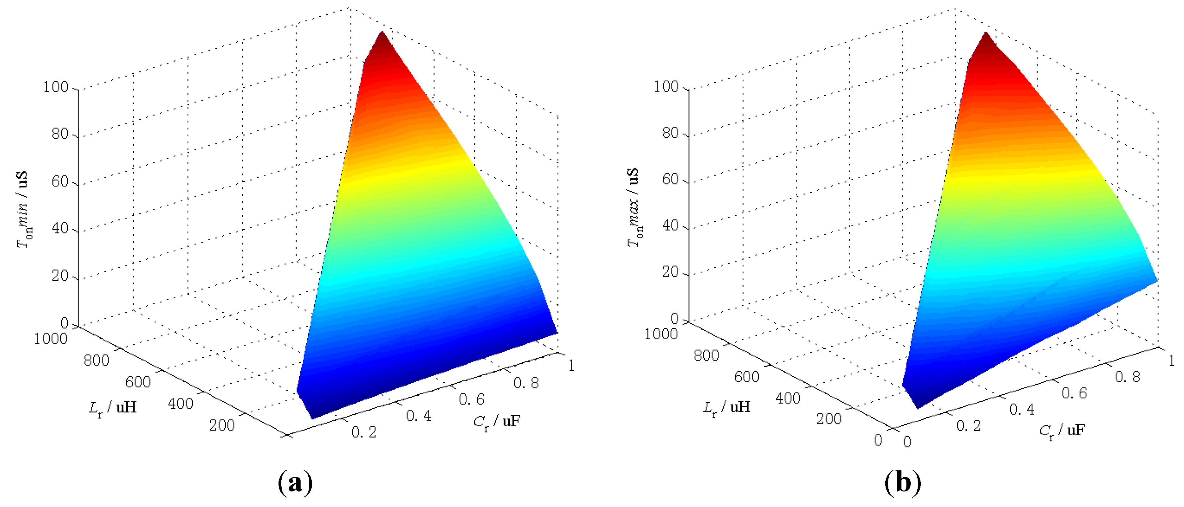
3.1.3. ZCS Boundary
Based on the above analysis and the constraints shown in Equations (35)–(40), the
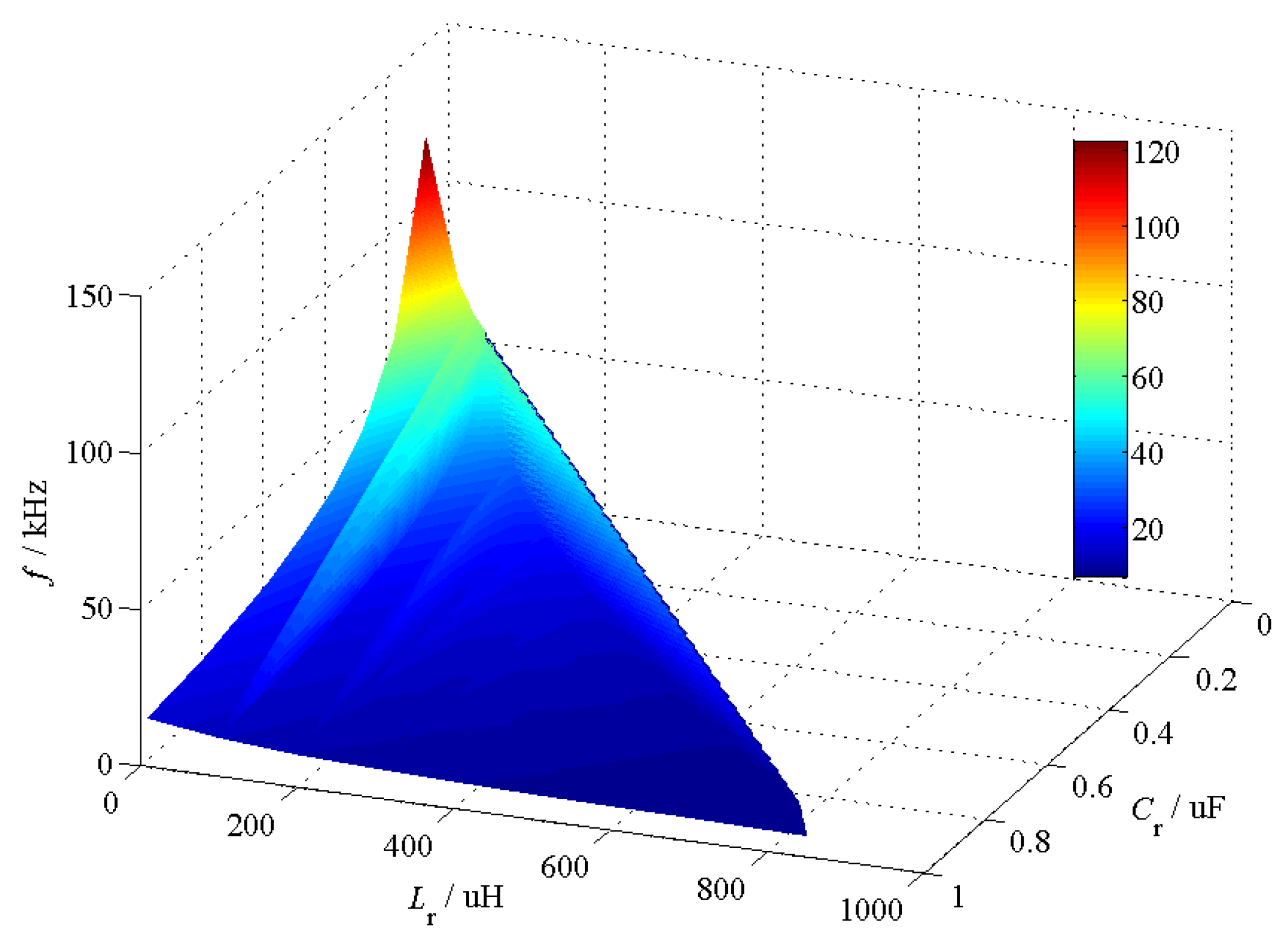
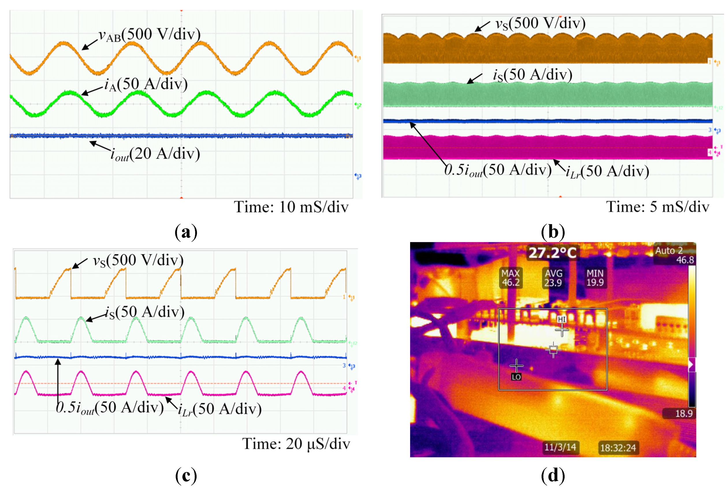
Ton range and ZCS boundary can be obtained, when the parameters of the resonant devices vary under the maximum power output condition (380-V input line voltage, 400-V output voltage, 8-Ohm load resistance).
Figure 10a,b illustrates the minimum and maximum
Ton value to realize ZCS, respectively. The driving frequency to satisfy the maximum output power with resonant device parameters changing is shown in
Figure 11.
Figure 10.
Minimum and maximum Ton value to realize zero-current-switching (ZCS). (a) minimum Ton and (b) maximum Ton.
Figure 10.
Minimum and maximum Ton value to realize zero-current-switching (ZCS). (a) minimum Ton and (b) maximum Ton.
Figure 11.
Driving frequency f to realize maximum output power.
Figure 11.
Driving frequency f to realize maximum output power.
3.2. ZCS and Battery
In this section, the cooperative control between ZCS realization and the three-stage battery charging method is studied, and the negative influence of battery charging status on ZCS realization is analyzed. Furthermore, a new method is presented to limit the minimum driving frequency when the battery is in a different status of charging.
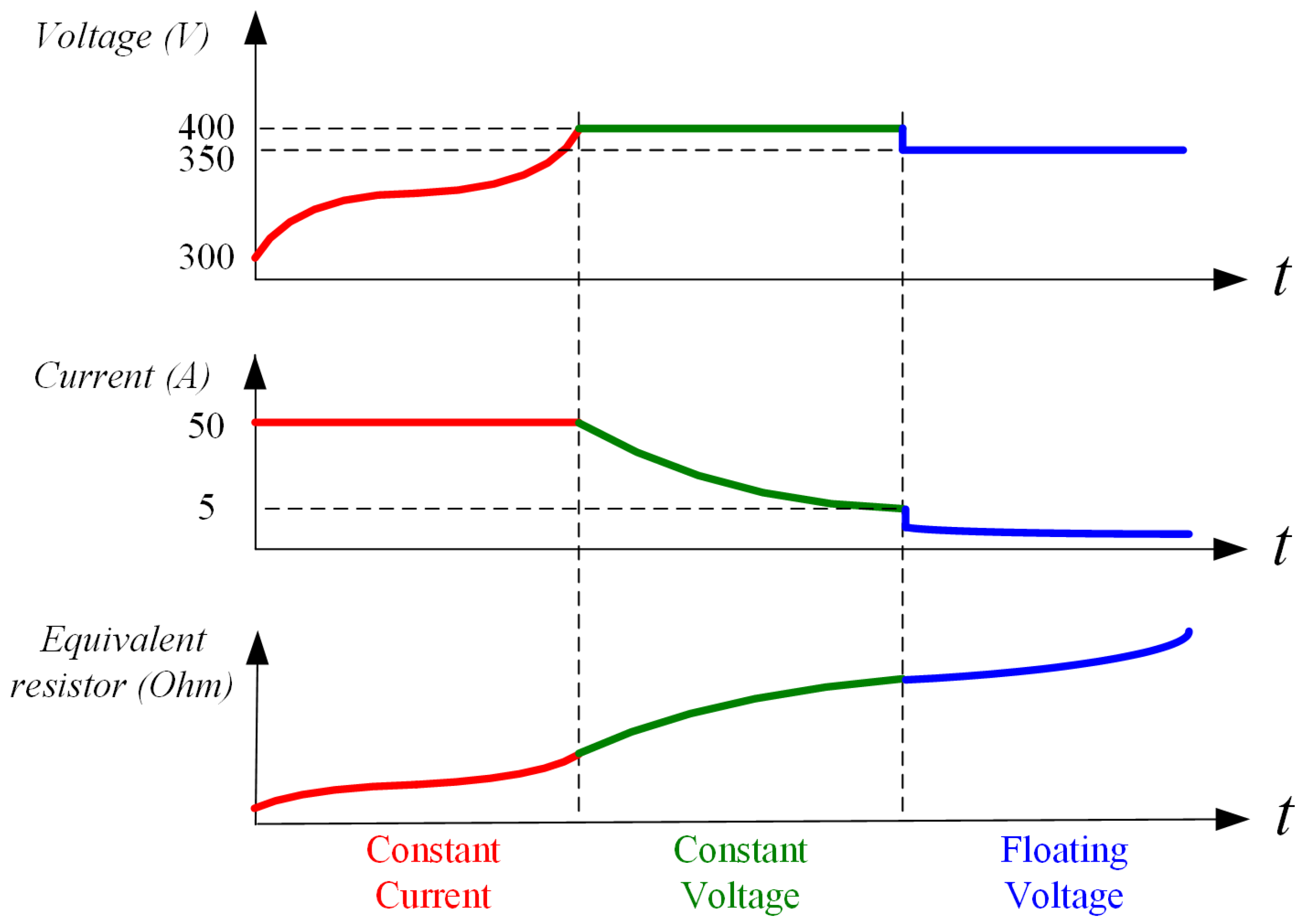
In order to optimize the charge cycles and lifetime of EV batteries, we adopt the three-stage charging method. The three stages are: constant current stage, constant voltage stage and floating voltage stage. During the constant current stage, the open-circuit voltage of the battery is about 300 V, and it is charged by a constant current of 50 A. The battery voltage increases with the charging process. When the voltage increases to 400 V, this stage ends, and the constant voltage stage begins. In the constant voltage stage, the charging voltage is 400 V, and the charging current will decrease; this stage ends when the current is below 5 A. The floating voltage stage is actually a low constant voltage stage to ensure a small charging current, to make sure that the battery is truly saturated to extend the service time. During this stage, the charging voltage is 350 V. The charging process and parameter settings are shown in
Figure 12 and
Table 1. Restricted by the experimental conditions, we use resistor load to simulate the batteries, and the equivalent resistor value is also shown in
Figure 12 and
Table 1.
Figure 12.
Three-stage charging process.
Figure 12.
Three-stage charging process.
Table 1.
Three-stage charging parameters.
Table 1.
Three-stage charging parameters.
| Stage | Iout (A) | Vout (V) | Rload (Ohm) |
|---|
| Constant current | 50 | 300–400 | 6–8 |
| Constant voltage | 50–5 | 400 | 8–80 |
| Floating voltage | 4.4–2 | 350 | 80–175 |
During the whole process of charging, the fluctuation range of the load equivalent resistance is very large. Just as the parameters shown in
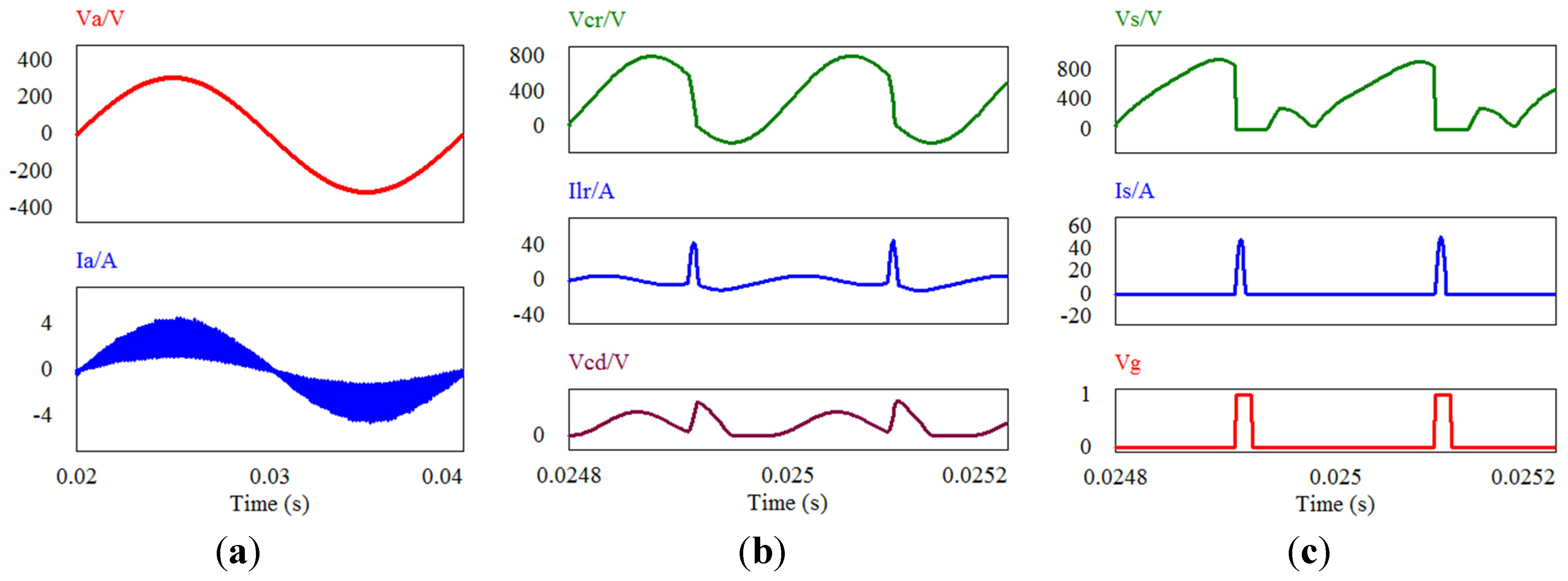
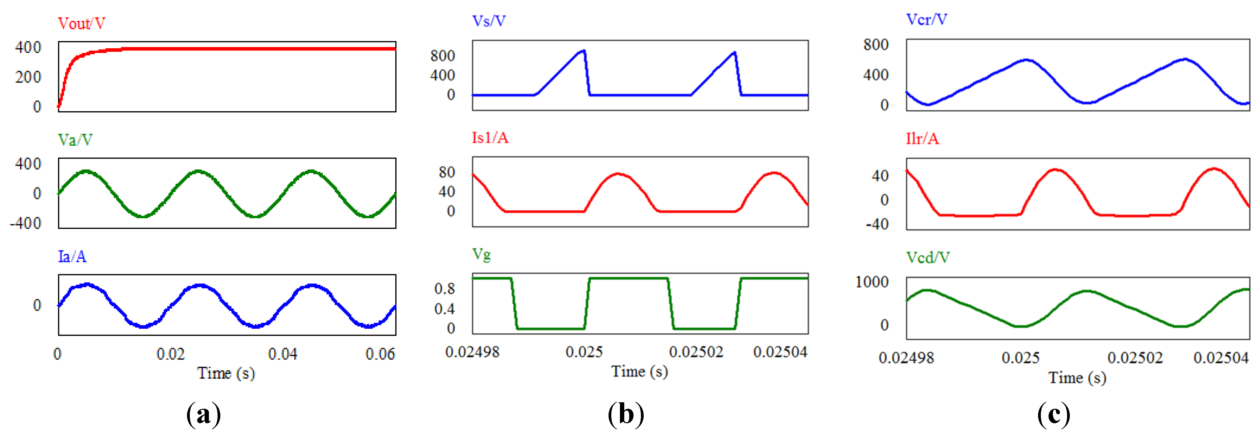
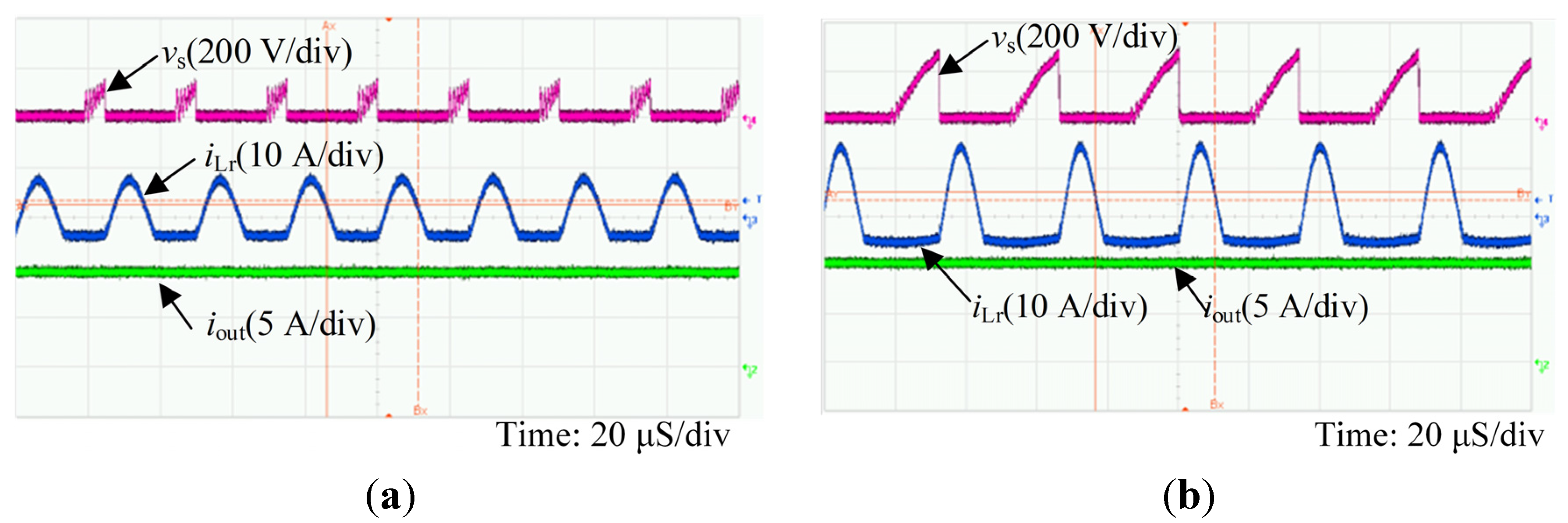
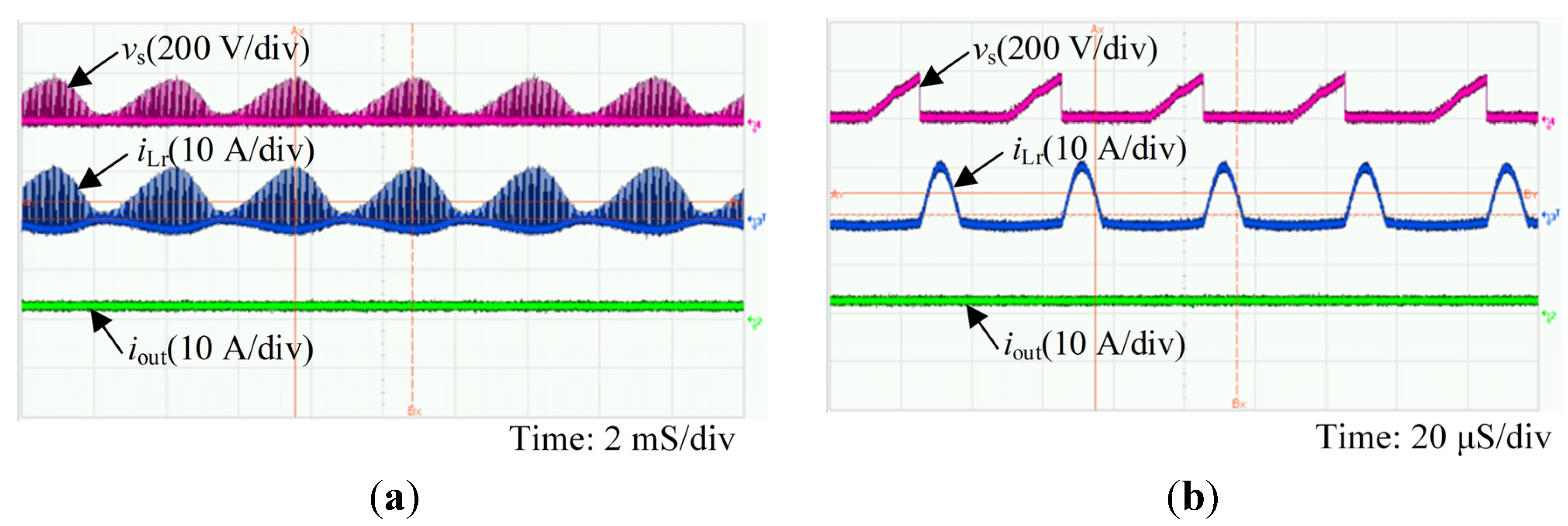
Table 1, at the end of the constant current stage, the charging power is the greatest at 20 kW. At the end of the floating voltage process, the minimum charging power is 0.7 kW. If we use the PFM control strategy during the whole process, the driving frequency variation range is very large. We select a point of the floating voltage stage as an example. If the equivalent resistor is 100 Ohm, the driving frequency should be 5.5 kHz to get a voltage output of 350 V. The simulation waveforms are shown in
Figure 13. From
Figure 13c, it can be seen that at this working point, the power switch
S works under the ZCS condition, while, the driving frequency is very low, so the turn off time is much longer than the resonant period of the resonant tank:
Lr,
Cr and
Cd. Therefore, before
S1 turns on, the resonant components will begin the next resonant cycle. Reactive power will be circulating in the tank, which will reduce the system efficiency and increase the THD of the input current.
Figure 13.
Simulation waveforms of the floating voltage charging stage. (a) input phase voltage and input phase current; (b) resonant capacitors voltage and resonant inductor current and (c) voltage and current of IGBT and gate signal.
Figure 13.
Simulation waveforms of the floating voltage charging stage. (a) input phase voltage and input phase current; (b) resonant capacitors voltage and resonant inductor current and (c) voltage and current of IGBT and gate signal.
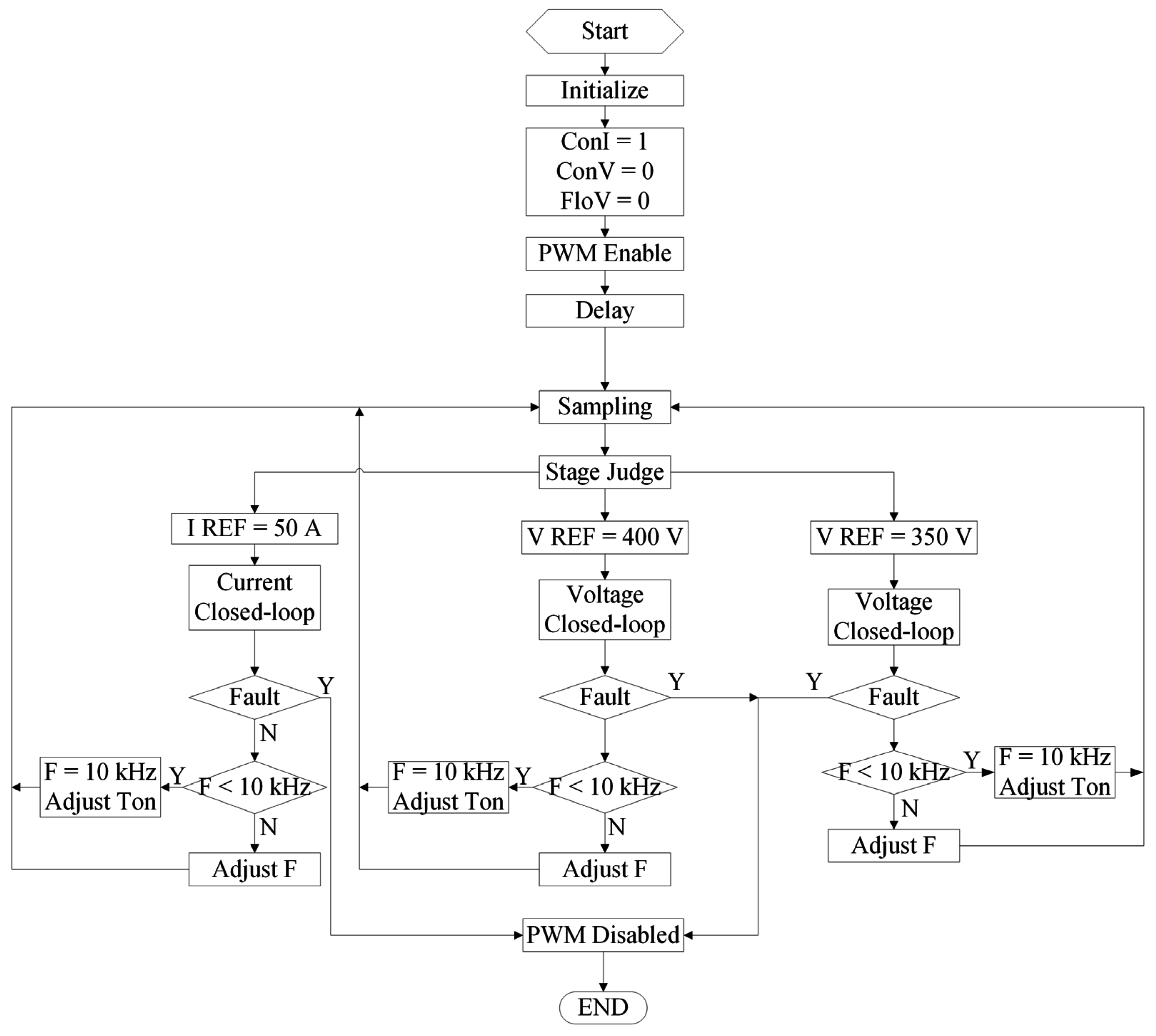
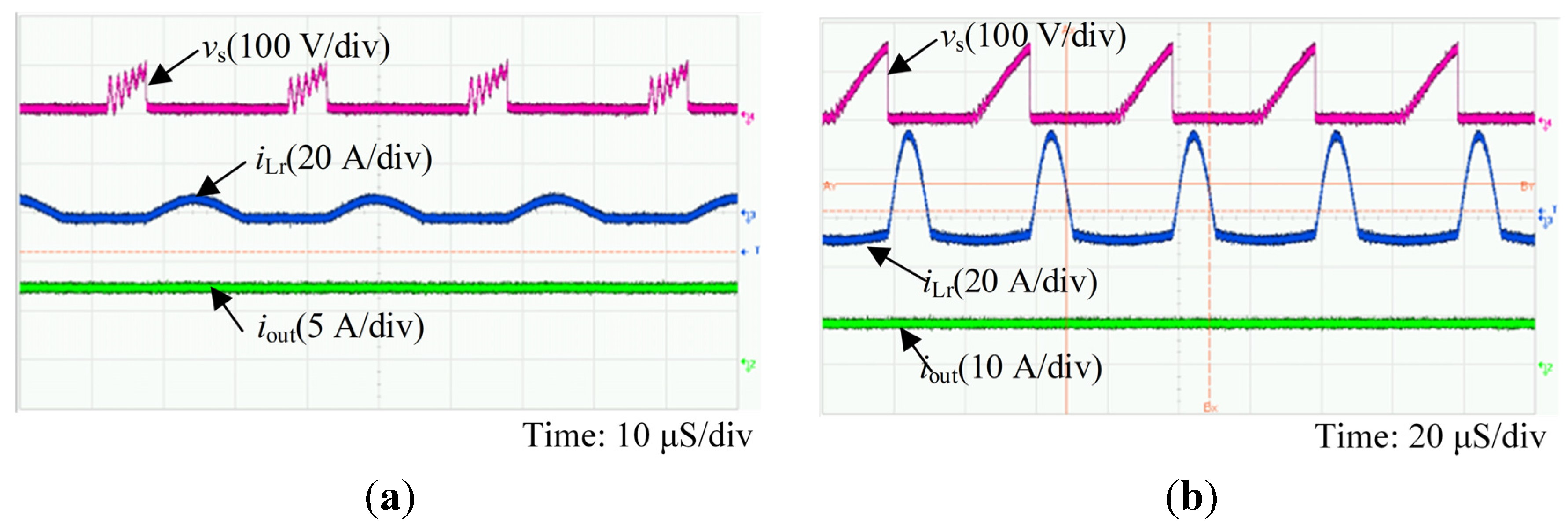
To solve the mentioned problem, we proposed a new control strategy. The complete control method of the system should be as follows: take the PFM control strategy at the beginning of the charging process (the conduction time is constant), and satisfy the output requirements by adjusting the frequency. If the PFM frequency is lower than 10 kHz, convert it to the PWM control strategy, keep the fixed driving frequency at 10 kHz and satisfy the output requirements by adjusting the conduction time
Ton. The charging process control flow chart is shown in
Figure 14.
By using the proposed control strategy, the minimum frequency is set at 10 kHz, and the frequency fluctuation will be reduced. Although the PWM strategy cannot guarantee ZCS realization, under the condition of a light load, the conduction losses increase greatly, are greater than the switching losses and seriously affect the system efficiency. Thus, using the PWM control strategy can contribute to the improvement of the system’s efficiency. What is more, this strategy can reduce the unexpected resonance on the resonant devices and power switches caused by a sharp drop of the driving frequency under a light load, which will lead to the increase of the input current THD.
Figure 14.
Charging process control flow chart.
Figure 14.
Charging process control flow chart.
3.3. Optimized Parameters
Considering the fact that the output voltage and current are changing during the whole charging process, we chose a set of circuit parameters that can ensure ZCS in the whole load range, as shown in
Table 2.
Table 2.
Main components of the prototype.
Table 2.
Main components of the prototype.
| Component | Value |
|---|
| Input filter inductors La–Lc | 2 mH |
| Resonant inductor Lr | 50 μH |
| Output filter inductor Lf | 800 μH |
| Input side resonant capacitors Cr1–Cr3 | 0.65 μF |
| Output side resonant capacitor Cd | 0.44 μF |
| Output filter capacitor Cf | 860 μF |
| Uncontrolled rectifier diodes D1–D6 | C3D25170H |
| Fly-wheel diode Dd | C3D25170H |
| Power switch S1 | IGW25T120 3 in parallel |
As shown in
Table 3, the power devices are selected at the maximum output current and voltage, which are 50 A and 400 V, respectively. From the interval analysis and Equations (7)–(34), we can calculate the voltage and current stresses of the main power devices in the circuit and finally determine the device type as follows.
Table 3.
Voltage and current stress of the main power devices.
Table 3.
Voltage and current stress of the main power devices.
| Component | Peak Voltage (V) | Voltage RMS (V) | Peak Current (A) | Current RMS (A) | Value |
|---|
| D1–D6 | 1170 | 440 | 95 | 20 | C3D25170H |
| Dd | 900 | 500 | 25 | 7 | C3D25170H |
| S1 | 1100 | 470 | 30 | 12 | IXBH42N170A 3 in parallel |
| La–Lc | - | - | 23 | 16 | - |
| Lr | - | - | 65 | 32 | - |
| Lf | - | - | 27 | 25 | - |
| Cd | 900 | 500 | 65 | 31 | - |
| Cr1–Cr3 | 650 | 270 | 75 | 25 | - |
3.4. Design of the Inductors
Besides the power switches and diodes selected above, the design of the inductors is very critical for the system design.
Through the theoretical analysis above, the currents of input filter inductors La–Lc and the output filter inductor Lf are sine wave shaped input current and non-oscillatory DC output current, respectively. Thus, the FeSi circular magnetic rings (PPF306060) are chosen to be the magnetic cores of the input and output filter inductors. Since the currents of the resonant inductors are a high-frequency resonant current with an extremely high peak value, a specially designed air gap is needed for the high frequency peak energy storage, and E-shaped magnetic cores (EE110) are selected for the resonant inductors.
3.4.2. Resonant Inductor
According to the theoretical analysis and simulation results, the resonant inductance is 50 μH, and the peak inductor current and RMS current are 65 A and 32 A, respectively. The inductor core is selected as EE110, and the material is PC-40 (MnZn power ferrite material). The turns of this inductor can be calculated as:
From the datasheet, Ae = 1296 mm2 and Bmax = 0.39 T. Thus, the turns can be deduced: N = 7.
3.4.3. Output Filter Inductor
According to the simulation results, the output filter inductance is 800 μH; the peak inductor current is 27 A; and the RMS current is 25 A. We also choose the magnetic core PPF306060 and use three cores in parallel. The number of turns can be calculated in the same way as Equation (41), and the parameters of this core are exactly the same as those of the input filters; finally, N = 54.
3.5. Loss Distribution
In this section, the power losses of the power switches, power diodes, inductors and capacitors at 50 A and 400 V output are estimated.
3.5.1. Power Switches
When calculating the power switch losses in the maximum power output condition, in view of the ZCS status of the power switches, we ignore the switching losses and only consider the conduction losses. The losses can be calculated by the following expression.
In Equation (43), D represents the duty ratio, VCESAT represents the drop voltage of the switch and IC represents the average current flow through the switch.
In the maximum power output condition, the driving frequency is about 35 kHz, so
D is about 0.53. The current of each switch can be approximated to a sine wave, shown in Equation (44), from zero to π. According to the datasheet of the switch,
VCESAT at this point is 2.1 V.
From Equations (43) and (44), the power loss of each power switch is:
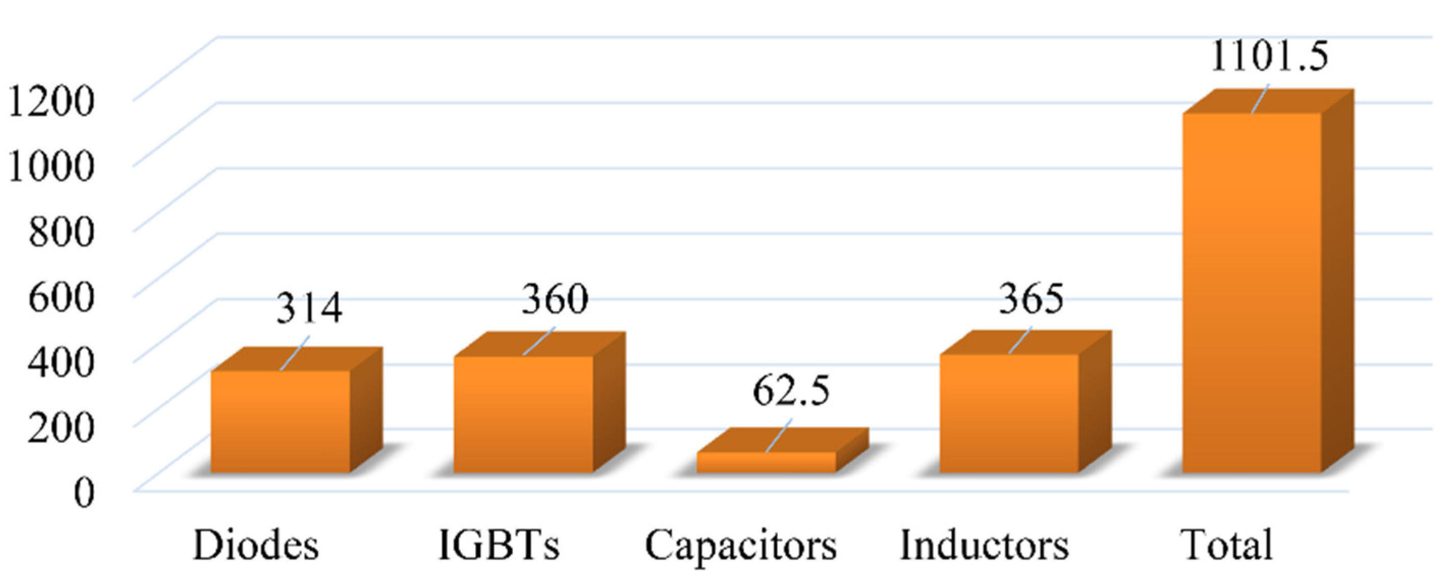
Thus, the total power loss of the 6 IGBTs is: PS = 6 × Pcond = 360 W.
3.5.2. Uncontrolled Rectifier Bridge Diodes
Just like the IGBTs, only conduction losses of the uncontrolled rectifier bridge diodes are considered:
According to the parameters shown in the datasheet and the operating point of the diodes, we can get that the power loss of each diode in the uncontrolled rectifier is 25 W.
Therefore, the total power losses of 12 uncontrolled rectifier diodes in the maximum power output condition can be shown as: PDBir = 12 × Pf = 300W.
3.5.3. Fly-Wheel Diodes
The calculating formula of fly-wheel diodes is the same as those of the rectifier diodes shown in Equations (46) and (47). Based on the interval analysis above, the current of the fly-wheel diodes is half of the output current. Thus, we can calculate the power loss for each fly-wheel diode to be about 7 W.
The total power loss of the two fly-wheel diodes in the maximum power output condition is 14 W.
The power dissipation of all the diodes in the OBC is: PD = PDBir + PDFly = 314 W.
3.5.4. Resonant and Filter Capacitors
The losses of the capacitors include two parts: dielectric loss and metal loss. The calculating expression is shown in Equations (48) and (49).
In Equations (48) and (49), RESR represents equivalent series resistance, tanθ0 represents the dielectric dissipation factor and tanθ represents the dissipation factor.
For the input side resonant capacitors, the datasheet gives that the tanθ is lower than 0.001, so we select the maximum value 0.001 as the dissipation factor. Considering that the dissipation angle is too small, the sine value can be approximated to the tangent value. Consequently, the power losses of the six input side resonant capacitors can be calculated as: PCr = 6 × (270 V × 25 A × 0.001) = 40.5 W.
The output side resonant capacitors use the same calculation and approximation method as the input side resonant capacitors. We use two 0.22-μF capacitors in parallel for each channel. The dissipation factor is lower than 0.006. Thus, the power losses of the four output side resonant capacitors can be calculated as: PCd = 4 × (500 V × 5 A × 0.0006) = 6 W.
Using the same calculation and approximation method, the power losses of the output filter capacitors can be calculated. We use two 430-μF capacitors in parallel for each channel, and the datasheet gives that the dissipation factor is lower than 0.002 at the operating point. Therefore, the power loss of the output filter capacitors is: PCf = 2 × (400 V × 10 A × 0.002) = 16 W.
Therefore, the total power losses of the capacitors in the OBC can be calculated as: PC = PCd + PCr + PCf = 62.5 W.
3.5.5. Resonant and Filter Inductors
The power losses of the inductor can be divided into two parts: core loss and winding loss.
For the magnetic core PPF306060, the core loss can be decided by the flux density and working frequency. The flux density can be calculated by the following expression.
where
B represents flux density (kG); μ represents relative permeability;
N represents the number of turns;
l means magnetic path length (cm);
I represents peak magnetic current (A);
f represents the working frequency (kHz) and
V represents the volume of the magnetic core (cm
3).
The winding loss is the heat loss caused by the coil resistance, and it can be calculated by Ohm’s law, shown in following expression.
From Equations (50)–(52), we can get the power losses of the six input filter inductors and the two output filter inductors, respectively, as: PLin = 6 × (Pcore + Pwire) = 72 W; PLf = 2 × (Pcore + Pwire) = 24 W.
For the resonant inductor, the winding loss is very small compared to the core loss. The core is designed as PC-40 EE110, where
Ve = 336,420 mm
3. According to the datasheet, the core loss per volume is obtained as:
Pcv = 0.0004 W/mm
3 at 60 °C. As a result, the core losses of two resonant inductors are:
Thus, the total power losses of the inductors in the system can be shown as: PL = PLr + PLin + PLf = 365 W.
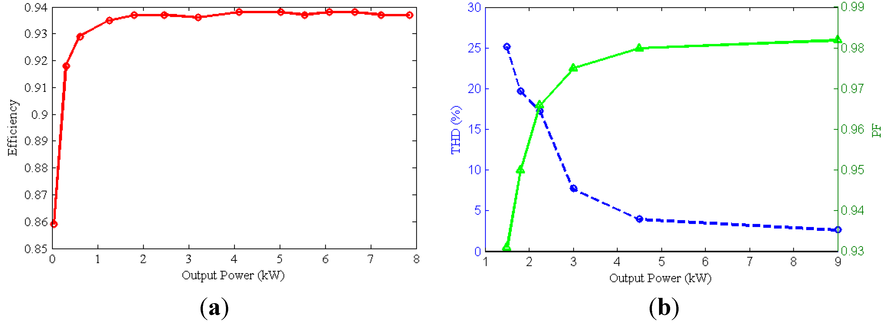
Finally, based on the calculation results shown in Equations (43)–(53), the conversion efficiency at the 20-kW output condition can be deduced as:
A power loss distribution under a 20-kW load is shown in
Figure 15. It can be concluded that the dissipation of this OBC mainly centralizes at the IGBTs, resonant inductors and bridge diodes. Additionally, this will be verified in the experiment section.
Figure 15.
Power loss distribution.
Figure 15.
Power loss distribution.


