3. Results and Analysis
During the thin film deposition, SiH4, CH4, and H2 gases are first decomposed into SiHn, Si, CHn, C, and H by the RF glow discharge. Then, the plasma reacts to generate Si–C, Si–CHn, and Si–Hn bonds, among others. Due to the presence of CHn, it is difficult to decompose into C atoms, compared to SiHn; although both SiHn and CHn are decomposed further by increasing the RF deposition power, more SiHn than CHn is decomposed under high RF deposition power. Therefore, the amorphous matrix obtained contains more silicon than carbon. To elucidate the effect of fast annealing on structural and light-emitting properties, the results are presented first without annealing and then compared with the annealing process.
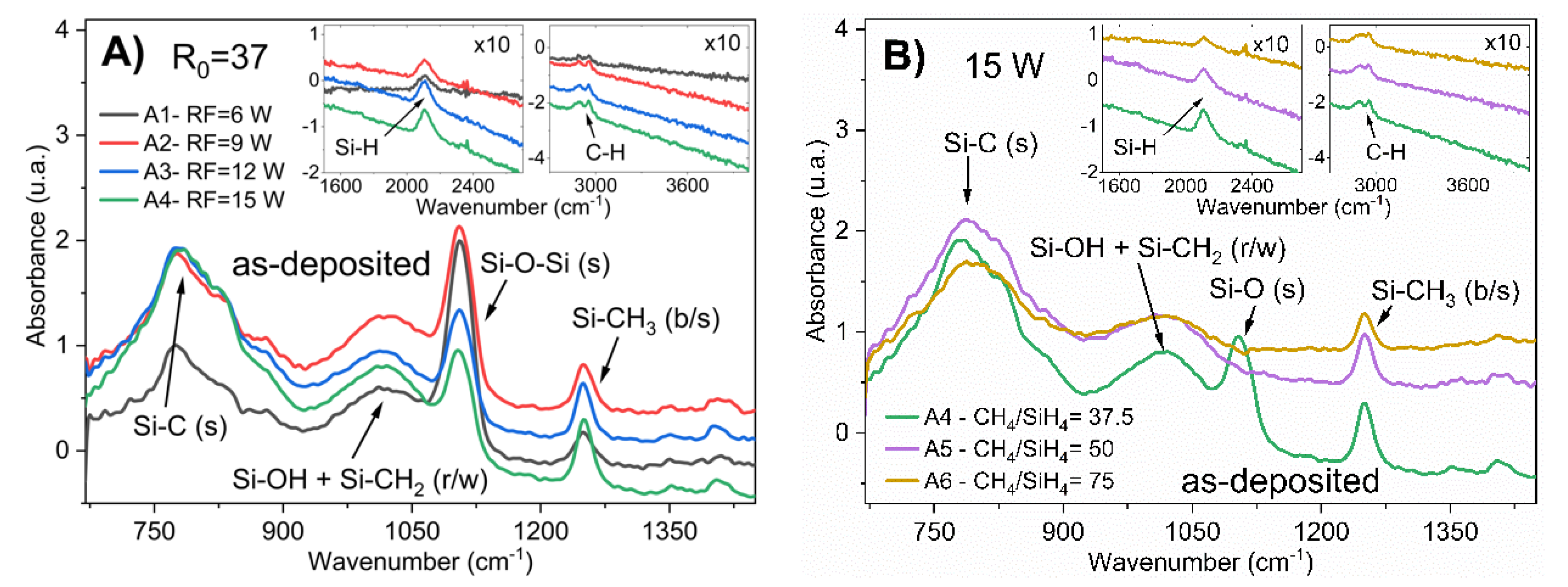
FTIR spectra revealed several bonding components in the as-deposited a-Si
1−xC
x:H material.
Figure 1A corresponds to a-Si
1−xC
x:H films deposited with different RF powers (6–15 W), keeping the CH
4/SiH
4 ratio constant; in contrast,
Figure 1B corresponds to a-Si
1−xC
x:H films deposited with different CH
4/SiH
4 ratios (R
0 from 37.5 to 75) with a constant RF power (15 W).
Considering the FTIR spectra of the as-deposited films, four main absorption bands can be observed: at 780 cm
−1, the Si–C stretching mode is located [
1,
13,
14]. The absorption band centered at 1015 cm
−1 is related to the rocking/wagging vibration modes of CH
2 radicals bonded to a silicon atom (Si–CH
2) [
15]; however, this band absorption can also be related to OH radicals bonded to silicon (Si–OH) [
16]. The strong and narrow peak at 1104 cm
−1 is associated with Si–O–Si stretching vibration. As the CH
3 symmetric (“umbrella”) deformation is strongly dependent on the electronegativity of the adjacent atom, the Si–CH
3 vibration is located at 1250 cm
−1 [
17]. Weak absorption was observed at ~1400 cm
−1, which is attributed to the C–H bending. Additionally, some absorption bands in the ranges of 2200–2000 cm
−1 and 3050–2850 cm
−1 were present, due to the Si–H and C–H stretching modes, respectively [
13,
15].
The FTIR measurements suggest the absence of a noticeable concentration of graphitic-like bonding configurations in the a-Si
1−xC
x:H, as no peaks were observed at 3000 cm
−1. It is important to remark that the FTIR measurement performed in an ambient nitrogen atmosphere could eliminate the false signals of triple bonds and cumulated double bonds (X≡Y and X=Y=Z) in the range of 2300–1900 cm
−1 [
16].
From the FTIR spectra, we can also observe some oxygen bonds, even when the a-Si
1−xC
x:H films were deposited with a vacuum system and without any oxygen (O) flow; therefore, there was some incorporation of O into the films, which could be attributed to some contaminants such as atmospheric oxygen (CO
2, H
2O, N
2), due to vacuum leaks, impurities in the gases, pump oil backstreaming (hydrocarbons), or from the absorption of reactor surfaces (H
2O) [
18]; moreover, the PECVD deposition parameters seem to have influenced the percentage of O incorporation. Therefore, the films could be considered to be an alloy composed of Si, C, and O; that is, an amorphous silicon hydrogenated oxycarbide [
14,
19].
The FTIR characterization provides information about the chemical bonding types which are present in the films, but is not very suitable for determining the content of each element. To clarify the compositional content of the films, EDS was employed.
Table 2 shows the atomic compositions obtained through the EDS characterization of the different a-Si
1−xC
x:H films. From the results, it can be observed that as the RF power increased, the Si content decreased; from 59. 28% at low RF power (6 W) to 50.02% at high RF power (15 W). At low RF power (6 W), the C content was 22.81%, which increased with the RF power; at high RF power (15 W), the C content was 36.61%.
According to the results of EDS, the carbon concentration was low for low RF powers (6 W). In addition, from the FTIR spectra shown in
Figure 1A, it is possible to observe that the use of low RF power (6 W) limited the formation of silicon–carbon bonds to obtain silicon carbide; thus, sample A1 was mainly composed of Si–O bonds and CH
2 and CH
3 radicals bonded to silicon. Samples deposited with a greater RF power than 6 W had a higher content of silicon–carbon bonds.
For low silane rates (R
0 = 50 and 75), the content of oxygen decreased. The FTIR spectra also presented a decrease in the silicon–oxygen bonds. In this way, the main absorption band was focused on silicon–carbon bonds. The A5 and A6 films were composed of silicon carbide, with CH
2 and CH
3 radicals bonded to silicon and a low concentration of Si–O bonds, as shown in
Figure 1B.
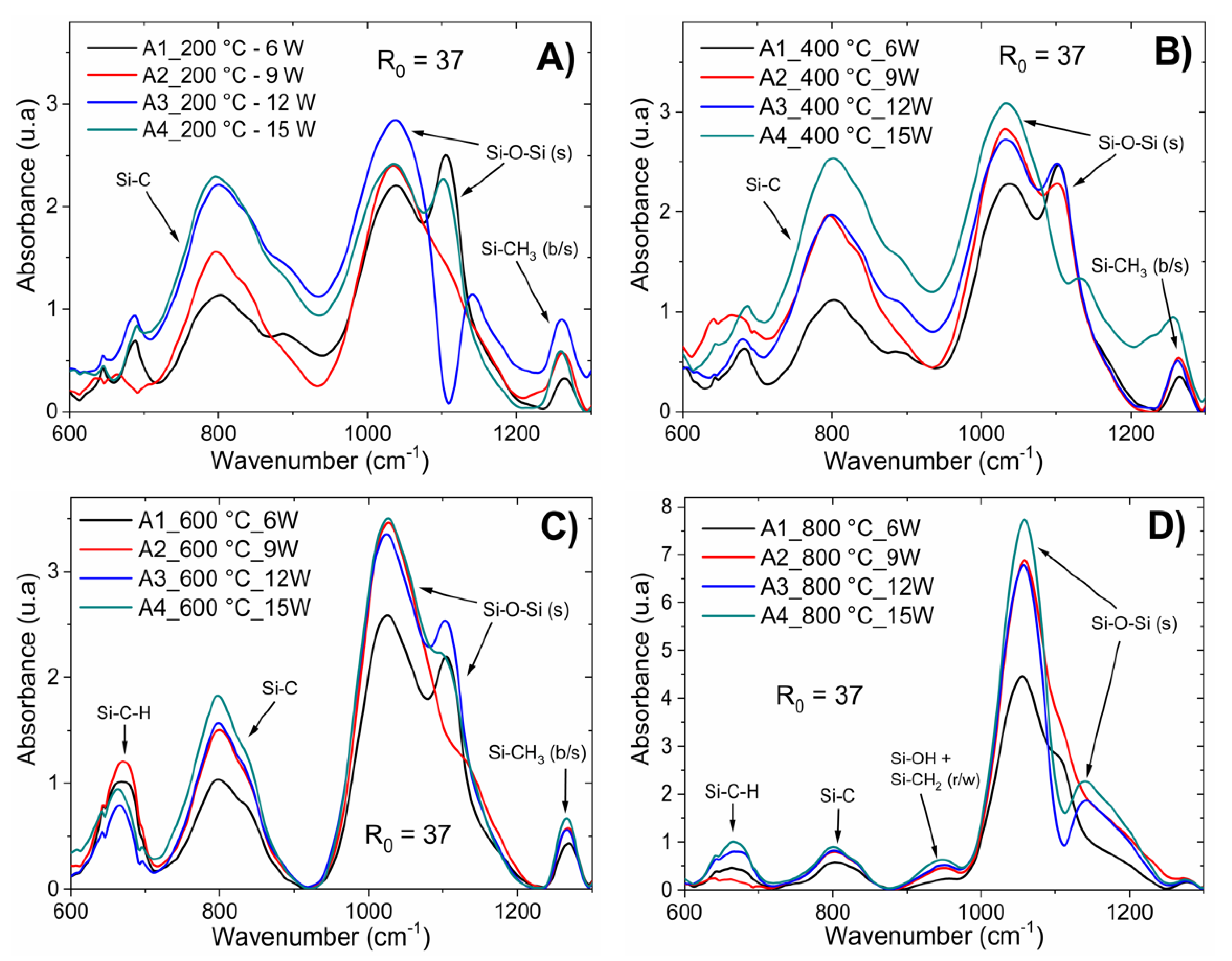
Chemical bonding was also observed to be dependent on the post-deposition thermal processing. IR spectra analysis for the six samples of a-Si
1−xC
x:H with annealing at 200, 400, 600, and 800 °C are shown in
Figure 2 and
Figure 3.
Figure 2 corresponds to a-Si
1−xC
x:H films deposited with different RF powers (6–15 W) keeping the CH
4/SiH
4 ratio constant; while
Figure 3 corresponds to a-Si
1−xC
x:H films deposited with different CH
4/SiH
4 ratios (R
0 from 37.5 to 75) with constant RF power (15 W).
The thin film samples were rapidly heated homogeneously. Thus, consequently, enough energy was gained for structural rearrangement. The main changes observed after annealing occurred in the Si–O–Si bonds in their different phases; as the temperature increased, the intensity of the absorption peak associated with this type of bond increased. This was correlated with the deposition parameters, as shown in
Figure 2 and
Figure 3. The increase in Si–O–Si bonds indicates that as the temperature increased during the annealing process, the degree of oxidation of the sample increased, which was observed for the temperatures of 600 and 800 °C. After the rapid thermal annealing, the Si–OH and Si–CH
2 bonds disappeared while for temperatures above 600 °C, a new absorption band centered at 663 cm
−1 appeared, which is associated with Si–C–H bonds. The absorption band related to Si–C bonding shifted to low frequencies and was centered at 808 cm
−1, as shown in labels (C) and (D) in
Figure 2 and
Figure 3. This structural rearrangement modified the light emission bands, as corroborated by the PL measurements.
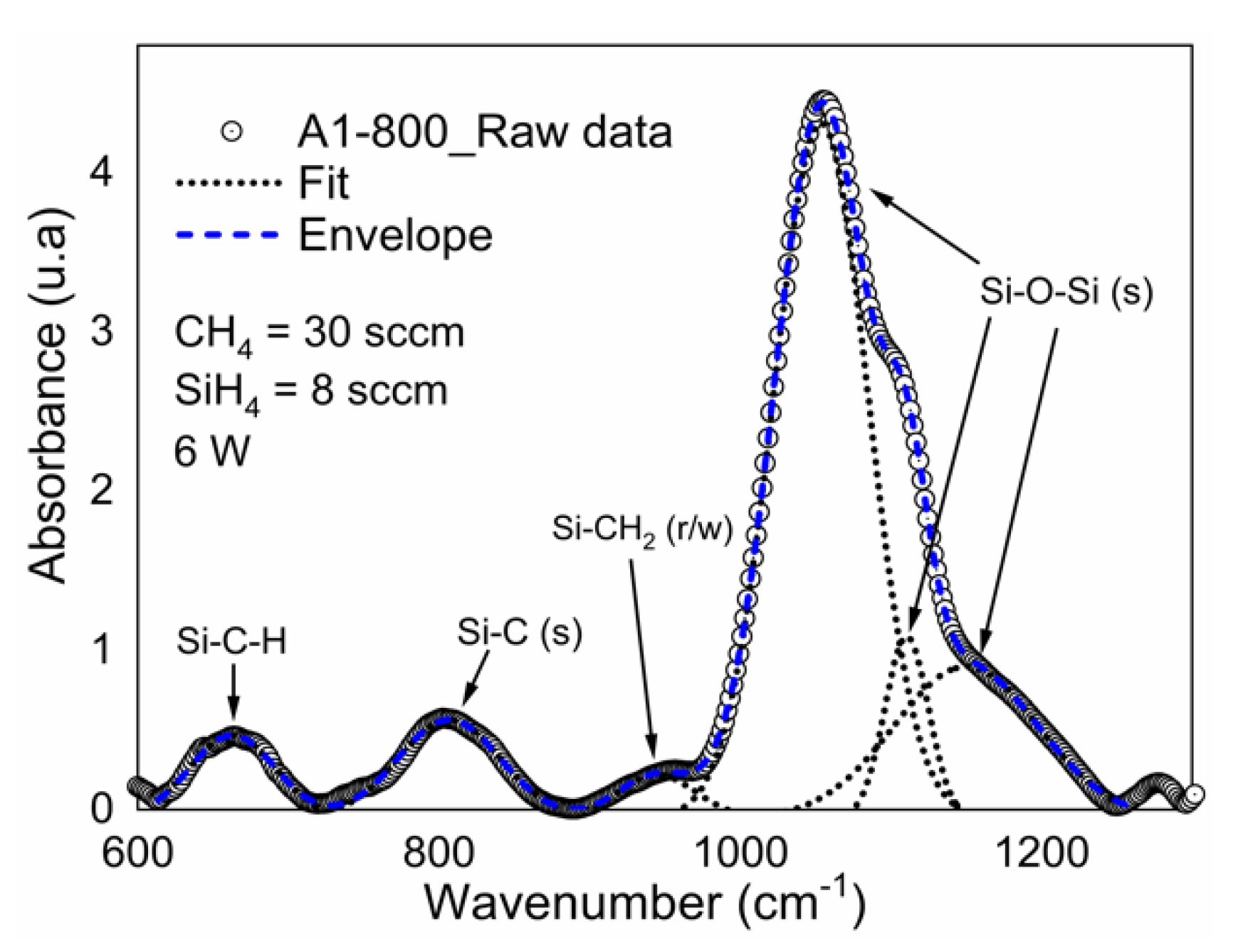
To confirm the degree of oxidation, the deconvolution of the A1 sample (6 W and R
0 = 37.5) with thermal annealing at 800 °C is shown in
Figure 4. The Levenberg–Marquardt algorithm was used for the deconvolution with a confidence of 95%.
Deconvolution of the main absorption band (Si–O–Si) shows three peaks centered at 1053 cm
−1, 1110 cm
−1, and 1149 cm
−1. The asymmetric stretching vibrations in which O atom motion occurs in the Si–O–Si plane parallel to a line joining the two silicon atoms are suggested to be responsible for the strongest absorption near 1053 cm
−1 [
13]. The presence of the three Si–O asymmetric stretching bands suggests the existence of three amorphous SiO
x phases, as correlated with changes in the Si–O–Si bonding angle. The peak at 1053 cm
−1 is attributed to a smaller Si–O–Si bond angle, considering the bond angle for stoichiometric silicon dioxide (144°), for which the peak is at 1080 cm
−1.
In this way, the main objective of this work is to enhance the light emission (PL) produced by a-Si1−xCx:H films when they are irradiated with ultraviolet (UV) light. The mechanisms that have been proposed to explain the photoluminescence in a-Si1−xCx:H are diverse, some of the main explanations are excitonic emission, quantum confinement of carriers in silicon nanocrystals inside the amorphous matrix, and emission due to localized defects.
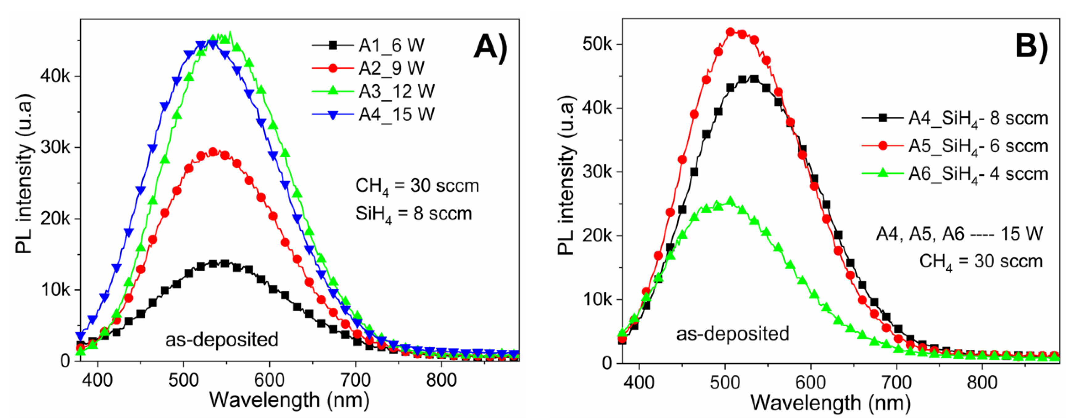
Figure 5A shows the PL spectra of as-deposited a-Si
1−xC
x:H films with different RF power (6–15 W) while keeping the CH
4/SiH
4 ratio (R
0 = 37.5) constant. From these spectra, it can be observed that the RF power had a strong effect on the PL intensity, with a clear increase of PL intensity observed as the RF power increases. Furthermore, the samples present luminescence throughout practically the entire visible range (i.e., 400–700 nm) with a peak intensity at 542 nm (2.28 eV). Notice that despite the PL intensity being affected by the deposition RF power, its Gaussian shape is not affected. The increase from 12 to 15 W in deposition power did not induce an increase in the photoluminescence intensity; however, there was a shift in the emission band (as the peak is located at 2.34 eV). These results are consistent in agreement with some previous studies [
20,
21].
The PL results showed significant changes in the intensity as a function of silane rate; however, no trend could be identified. In
Figure 5, the PL peak position shifts from 530 nm (at 2.33 eV) to 490 nm (at 2.53 eV) when the CH
4/SiH
4 flow rate ratio increases from 37.5 to 75. This shift could be due to changes in the amorphous matrix, as shown in
Figure 1B, causing stress in the localized states resulting in light emission.
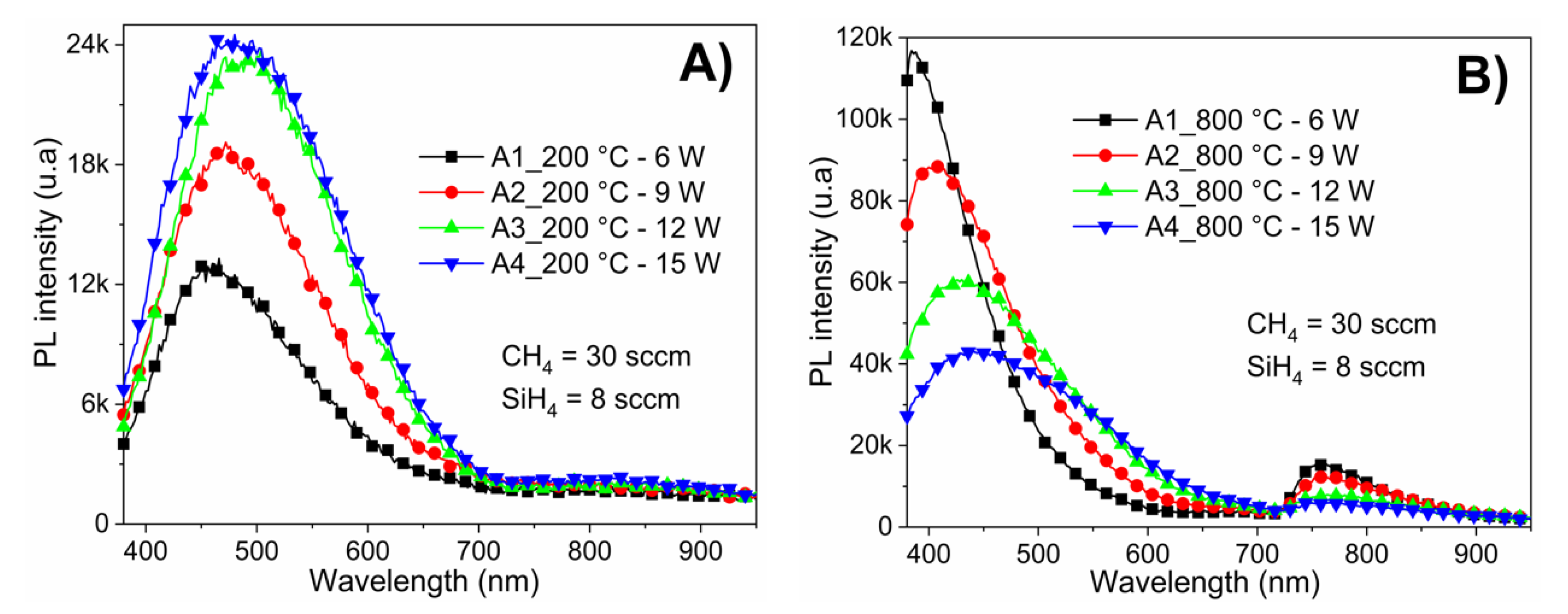
PL spectra after annealing treatment of a-Si
1−xC
x:H films deposited with different RF powers and constant ratio R
0 =37.5 are shown in
Figure 6A,B, annealed at 200 and 800 °C, respectively. Samples annealed at low temperature (200 °C) had a lower luminescence intensity than samples annealed at high temperature (800 °C); furthermore, the maximum emission peaks shifted towards shorter wavelengths (higher energies) as a function of the annealing temperature.
In sample A1, the PL peak position of the as-deposited film was located at 544 nm, which shifted to 461 nm when annealing at 200 °C, and to 385 nm when annealing at 800 °C.
Notice that the samples annealed at high temperature (800 °C),
Figure 6B have two emission bands; sample A2 (R
0 = 37.5 and RF power = 9 W) has an intense emission band over almost the entire visible range (380–602 nm) with a maximum peak at 405 nm, as well as another low-intensity emission band in the near infrared (728–847 nm). Samples annealed at 200 °C only have one PL emission band covering almost the entire visible range (380–706 nm), as shown in
Figure 6A. In fact, samples with annealing at 600 and 800 C show two emission bands; while those annealed at 200 and 400 only have one band. The emission band in the near infrared have been reported in silicon oxides [
22,
23]; this suggests that the oxidation degree increases with the annealing temperature. In the
supplementary material (Figures from S1–S10) section, a qualitative comparison of normalized photoluminescence for different conditions of deposition is shown.
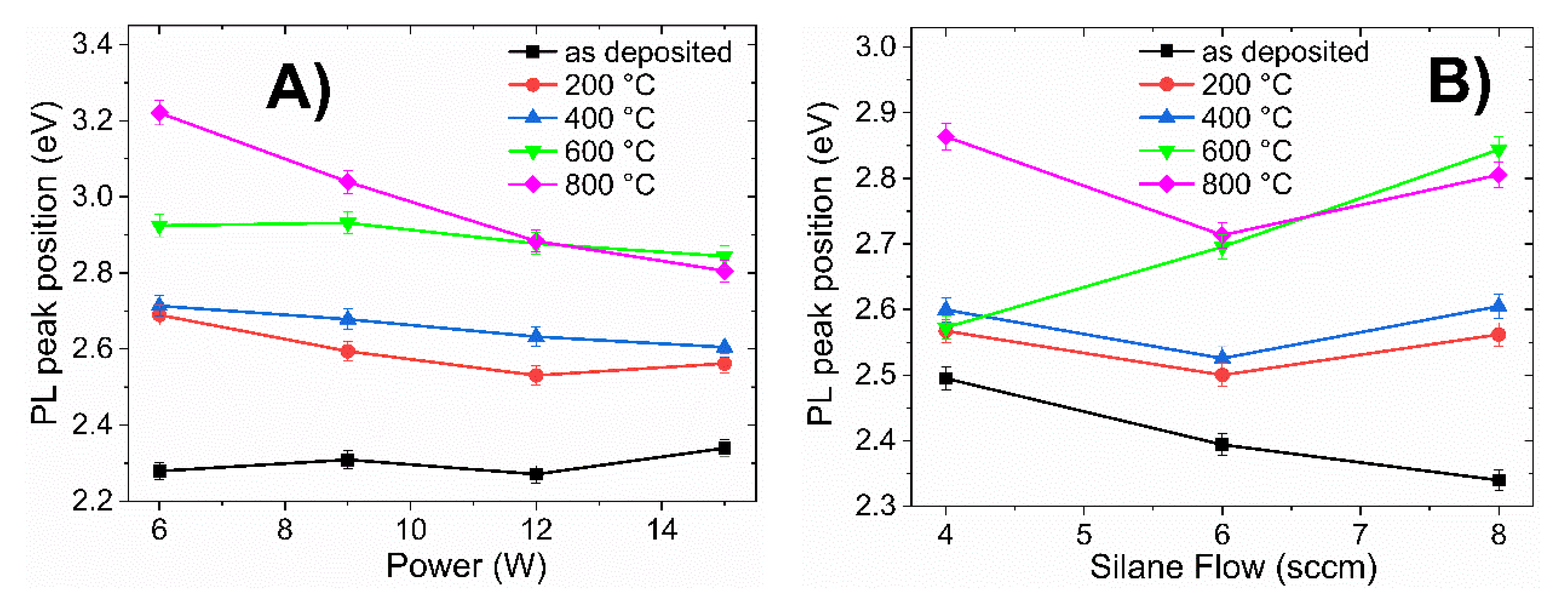
To summarize the PL results,
Figure 7 presents the maximum PL peak position of all films as a function of RF power, R
0 ratio, and annealing temperature.
Figure 7A corresponds to films with different RF powers (6–15 W) at R
0 = 37.5;
Figure 7B corresponds to those films deposited with a fixed RF power (15 W) and differing R
0 (37.5–75).
From
Figure 7A the PL peak position in as-deposited films is practically kept constant as a function of power (black line in
Figure 7A); however, after fast annealing, the PL peak position strongly depends on the annealing temperature. All samples deposited with R
0 =37.5 presented a shifting in the peak and light emission band towards the blue as the annealing temperature increased, regardless of the deposition power. This correlated with the FTIR results and corresponded to an increase in the degree of oxidation. The effect was noticeable for the film deposited with a low RF power (A1; 6 W), with PL peak located at 2.28, 2.69, 2.71, 2.92, and 3.22 eV for the sample without annealing and annealing temperatures at 200, 400, 600, and 800 °C, respectively. The PL peak position experienced a 0.94 eV (159 nm, from green to violet) strong shift towards higher energies.
According to X-ray Diffraction (XRD) and High-Resolution Transmission Electron Microscopy (HRTEM) measurements, the structural matrix was amorphous in the deposited samples; there was no evidence of the presence of silicon nanocrystals before or after the annealing process (see
supplementary material, Figure S11). Therefore, the displacement PL peak position cannot be associated with carrier quantum confinement. Thus, the light emission of the films obtained in this work was associated with recombination processes in localized states and the change in the PL peak position was due to changes in the bond angles of the luminescence centers. For example, in sample A1 (6 W and R
0 = 37.5), the shift of the PL peak position was accompanied by a strong increase in the light emission intensity, which suggests that the increase of light emission was due to an increase in the recombination centers in the amorphous silicon oxycarbide; the alloys formed during the rapid annealing process.
Shifting of the PL peak position was also observed for the samples deposited with different R
0 ratio, as shown in
Figure 7B. The displacement of PL peak position was small for the sample deposited with high ratio R
0 (75) at temperatures below 600 °C (i.e., 0.1 eV with respect to the sample without annealing); however, when the temperature rose to 800 °C, an abrupt shift in PL peak position can be observed (from 2.5 eV to 2.87 eV).
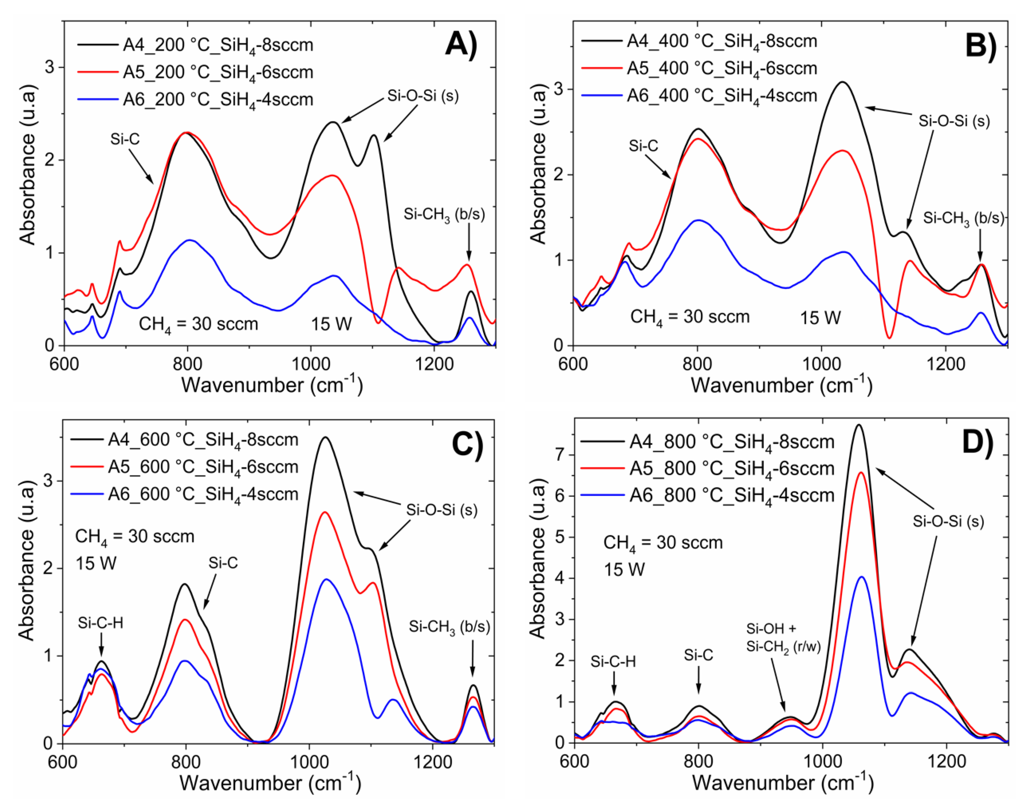
According to the EDS results, as the silane flow decreases, the oxygen content decreases; thus, low silane flow limits the incorporation of oxygen.
Figure 3C shows the FTIR spectra for the samples deposited with different silane flows annealed at 600 °C, from which it can be observed that the oxygen content had a strong influence on bond rearrangement during annealing: as the oxygen content decreased, the intensity of the asymmetric Si–O–Si stretching band decreased and shifted toward higher wavenumbers. The decrease intensity and shifting of this absorption band caused a strong shift in the PL peak position, as shown in
Figure 7B.
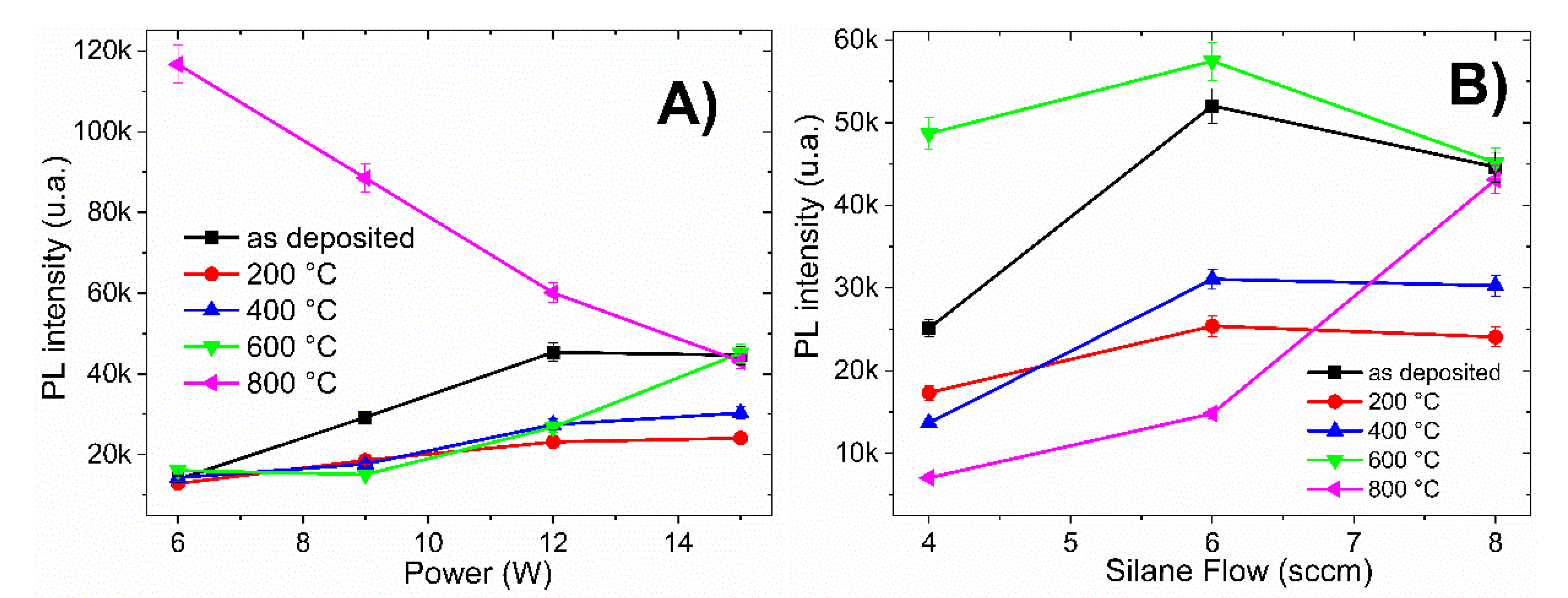
Another important aspect to consider is the change in PL intensity with respect to the annealing temperature.
Figure 8 presents the PL intensity as a function of RF power, CH
4/SiH
4 ratio, and annealing temperature.
Figure 8A corresponds to films with different RF powers (6–15 W) keeping the CH
4/SiH
4 ratio (R
0 = 37.5) constant; while
Figure 8B corresponds to films deposited with different CH
4/SiH
4 ratios (R
0 = 37.5–75) at constant RF power (15 W).
The samples annealed at high temperatures (800 °C) showed a strong improvement in PL intensity when the gas flow ratio and the RF power deposition were low (R
0 = 37.5; 6 W, 9 W, and 12 W), as shown in
Figure 8A. Meanwhile, for samples deposited with low silane flow (4 sccm and 6 sccm in
Figure 8B, the maximum PL intensities were obtained with annealing at 600 °C.
The PL peak position of all films with thermal treatment at temperatures below 400 °C (
Figure 7) shifted towards blue, depending in the degree of oxidation and the carbon, oxygen, or silicon content; however, the intensity of light emission decreased and there was only one emission band.
Sample A1 (R
0 = 37.5 and 6 W RF power) showed an increase in PL intensity of more than nine times with annealing temperature at 800 °C, in contrast to the sample without annealing, as can be observed in
Figure 8A. From the EDS results and
Figure 8B, when the sample has a high carbon content and a low oxygen content, an improvement in PL intensity is obtained at 600 °C.
Many structural defects in silicon-based materials, such as Si-related oxygen deficiency centers (Si-ODCs; e.g., O3≡Si…Si≡O3), non-bridging oxygen hole centers (NBOHCs) whose structure is identified by its paramagnetic properties and is denoted by ≡Si-O• (where (≡) stands for bonds with three oxygens and (•) indicates an unpaired electron), Si-related oxygen vacancies (Si-NOVs), and C-related oxygen vacancies (C-NOVs), are known to be luminescent in the UV/visible range. For example, NBOHCs yield red (~2 eV) emission, while Si-ODCs and Si-NOVs or C-NOVs result in green and blue emission, respectively, in the ranges of 2–2.4 eV and ~2.8 eV [
7,
10,
24,
25]. Therefore, the dynamic behavior of photoluminescence observed in the deposited films can be inferred to have originated from defect states.

 ,
, 


