1. Introduction
The epitaxial growth of silicon, silicon-germanium (SiGe) layers on a silicon substrate is a well-established technology for semiconductor fabrication, and has long been applied to the production of high-performance image sensors [
1] and power devices [
2]. Moreover, the addition of phosphorus or boron precursors along with the Si precursor enables the growth of Si:P or Si:B alloys with much higher P or B doping concentrations than can be obtained via ion implantation [
3,
4,
5,
6]. In addition to Si, Group 4 elements such as Ge, C, etc. can be applied to stress engineering [
7,
8,
9,
10]. This enables a source/drain (S/D) strain engineering in which SiC epitaxy is used to increase electron mobility by providing tensile strain, while SiGe epitaxy is used to increase hole mobility by providing compressive strain. Further, relaxed epitaxy technology can be used to grow Ge as a relaxed-Ge channel with very high hole mobility [
11]. Currently, epitaxy technology is a key process for the continued scaling and increased functionality of integrated circuits. With respect to scaling, the currently used FIN field-effect transistor (FINFET) technology has been extended down to 5 nm, but the most suitable structure for the 3 to 2 nm scale downwards is probably the gate-all-around FET (GAAFET) [
12,
13]. A key process for implementing the GAAFET is the stacked epitaxial growth of Si and SiGe to construct multi-layers of nanosheets.
The chemical vapor deposition (CVD) processes used for epitaxial growth includes ultra-high vacuum CVD (UHVCVD) [
14], reduced pressure CVD (RPCVD) [
15,
16], and atmospheric-pressure CVD (APCVD) [
17]. Among these, RPCVD has the advantage of combining a high throughput with high quality epitaxy. While several papers have reported the growth of crystalline Si or SiGe [
18,
19,
20,
21,
22,
23,
24], there are a few reports on key process steps in low-temperature epitaxial growth via RPCVD. In addition, many reports using dichlorosilane (DCS) as Si source have been performed at high temperature above 700 °C [
18,
19,
20,
21,
22,
23] due to poor chlorine (Cl) desorption of DCS at low temperature. Even though high order silane precursors can be used at lower temperature [
24,
25,
26,
27], a cyclic deposition and etch routine are needed for selective epitaxial growth (SEG), making DCS the most common Si precursor for SEG of Si and SiGe. Epitaxial growth is performed via several sequential steps. The first step is pre-treatment of the wafers, which usually involves an initial ex-situ wet cleaning step, after which the wafers are loaded into a load lock chamber of the RPCVD system. From there, the wafers are moved via a transfer chamber into either an additional in-situ cleaning chamber or directly into the process chamber, where a final pre-cleaning step such as H
2 bake takes place. Finally, the epitaxial growth occurs in the process chamber (
Figure 1). Each of these process steps need to be well tuned to grow high-quality epitaxial films. In particular, the most representative interface impurities in Si and SiGe epitaxy are oxygen (O), carbon (C), and fluorine (F). The presence of O at the interface of Si and epitaxial layer leads to staking faults in the Si film [
28], while C leads to the precipitation of silicon carbide and causes dislocation or staking faults in the Si lattice. Meanwhile, surface-adsorbed F is unstable, such that Si–F bonds are easily transformed into Si–H–O bonds during the extended queue time under ambient atmosphere, thus promoting re-oxidation after the surface cleaning [
20,
29].
Therefore, the use of RPCVD equipment and processes that are free from impurities, or at least suppress impurities as much as possible, are essential. In the present paper, several key process steps are examined using a 300 mm cluster RPCVD system at a temperature as low as 700 °C with DCS precursor. First, for the application of ex-situ cleaning, wet cleaning with dilute hydrofluoric acid (DHF), dry cleaning, and a combination of wet and dry cleaning are compared. Then the effects of in-situ bake with H2 at various temperatures, and the effects of two-step baking with H2 followed by HCl, are investigated. Finally, the effects of the temperature and environment of the process chamber at the time of loading the wafers are examined.
2. Experimental Details
The epitaxy equipment used in the present work is an industrial RPCVD tool with a planetary reactor for the simultaneous loading of up to five 300 mm wafers on each satellite mounted on a graphite susceptor (Wonik IPS Co., Pyeongtaek, Korea). The susceptor and satellites rotate in synchrony to provide epitaxially grown films with highly uniform thicknesses. The precursors are injected through the shower heads in the middle of the reactor and are discharged through the outlet at the edge of the susceptor. The detailed reactor structure and modeling of the resulting CVD growth have been provided in previous work [
30,
31]. Before loading the p-type (100) 300 mm wafers into the epitaxial equipment, the wafers were cleaned with DHF (single wafer spin wet etcher, Apollon, Zeus. Co., Hwaseong, Korea). Starting from a stock solution of 49% HF, two concentrations of DHF solution were prepared in deionized (DI) water, namely 1:30 DHF/DI water (1.58% DHF, 0.932 M) and 1:200 DHF/DI water (0.24% DHF, 0.143 M).
These solutions were compared for the pre-cleaning of the Si wafer. The cleaning times were adjusted based on the thermal oxide etching of about 5 nm. After the spin etching, the wafers were spin rinsed with DI water and then spin dried.
In addition, the ex-situ 1:200 DHF wet cleaning process was compared with dry cleaning and with a combination of 1:200 DHF wet + dry cleaning. The ex-situ dry cleaning process was performed using NF3/NH3 plasma. The queue time in the atmosphere was minimized after dry cleaning, the samples were loaded into the chamber, and Si epitaxial films were grown under the same conditions as for the wet-cleaned wafer.
In another set of experiments, the effects of additional in-situ bake in the presence of H2 only, or H2 followed by HCl were compared. The (100) Si wafers were first subjected to ex-situ wet cleaning with 1:200 DHF or ex-situ dry cleaning. Unless otherwise noted, the cleaned wafers were moved from the transfer chamber to the process chamber under vacuum. The loaded wafers were then subjected to in-situ bake at 700 °C for 10 min or at 750, 800, or 850 °C for 5 or 10 min in the presence of H2 and/or HCl. After baking, the dichloro-silane (DCS, SiH2Cl2), germane (GeH4), H2, and HCl were used for Si, SiGe blanket and selective epitaxy at 700 °C under pressures of 10–100 Torr.
In further experiments, the effects of the temperature and environment of the process chamber at the time of loading the wafers were examined. In these experiments, all the wafers were subjected to ex-situ dry cleaning before loading into the equipment. After dry cleaning, the wafers were loaded into a load lock chamber and subjected to vacuum before being moved into a transfer chamber and, finally, into the process chamber. The temperature of the process chamber at the transferal stage (i.e., the loading temperature) was varied as 550, 600, 650, and 700 °C, and the conditions of the process chamber were either a vacuum or a gaseous atmosphere.
The thicknesses and quality of the resulting epitaxial films were examined via Cs-corrected scanning transmission electron microscopy (HRTEM; JEOL, JEM-ARM200F, Tokyo, Japan) and secondary ion mass spectroscopy (SIMS; IMS 7f, CAMECA, Gennevilliers, France). O (16O), F (19F), and C (12C) concentration profiles were measured with a SIMS Cameca IMS 7f microanalyzer by using a 6 keV Cs+ mass-filtered primary ions of an intensity of 12 nA. The beam was rastered over an area of 250 × 250 μm2 and the analysis area was 150 μm in diameter. The quality of the epitaxial SiGe film was measured by high resolution X-ray diffraction (HRXRD) using PANalytical X’pert PRO (Malvern, UK) with a 4 bounce symmetric Ge (220) monochromator and slits in front of the detector.
3. Results and Discussions
3.1. Ex-Situ Wet DHF Cleaning
The concentrations of impurities in the SiGe epitaxial films obtained after pre-cleaning with 1:30 DHF and 1:200 DHF are indicated by the SIMS results in
Figure 2. The SiGe film grown after cleaning with 1:30 DHF exhibits an O peak with a concentration of about ~10
20/cm
3 at the interface between the SiGe film and the Si substrate, whereas the film grown after cleaning with 1:200 DHF exhibits a decreased concentration of ~10
19/cm
3 (
Figure 2a). Similarly, the level of F impurity is less in the film grown after cleaning with 1:200 DHF (
Figure 2b). This may be attributed to the formation of more Si–H bonds, and correspondingly fewer unstable Si–F bonds, on the Si surface during the longer etching time in the presence of the lower-concentration HF solution (1:200 HF).
3.2. Comparison of Ex-Situ DHF Wet Cleaning, Dry Cleaning, and Combined Wet + Dry Cleaning
The SIMS profiles of the Si epitaxial films obtained after ex-situ wet pre-cleaning with 1:200 DHF, dry cleaning, and combined wet + dry cleaning are presented in
Figure 3. Thus, in
Figure 3a, the O profile of the epitaxial substrate that was wet cleaned with 1:200 DHF exhibits an impurity peak with a concentration of ~1.8 × 10
18/cm
3. By comparison, the intensity of the O peaks of the dry cleaned and wet + dry cleaned substrates are measurably decreased. Among the dry and wet + dry cleaning, the wet + dry have a lower O concentration at the interface. Meanwhile, the F profiles in
Figure 3b reveal a major decrease in the level of F impurity for the dry and the combined wet + dry cleaning, compared to the wet-only treatment, while the C profiles in
Figure 3c reveal no impurity peak for all three cleaning conditions. These results can be attributed to the fact that the Si surface becomes H-terminated and hydrophobic when pre-cleaning is performed using DHF, which can prevent pollution or oxidation in the ambient atmosphere. However, in the case of the wet-only cleaning, the amount of subsequent queueing time in the ambient atmosphere is inevitably increased by the need for rinsing with DI water followed by drying. This significantly increases the possibility of re-oxidation. Not only is the need for these processes eliminated in the case of dry cleaning, but also there is the advantage of being able to perform the in-situ dry cleaning in a vacuum chamber. Hence, dry cleaning is more advantageous than wet cleaning in terms of the queue time constraints. The TEM images of the interface between the Si epitaxial layer and the Si substrate of the epitaxial films grown after the three different pre-cleaning are presented in
Figure 4. Here, the interface between the substrate and the epitaxial layer is easily distinguished in the sample that was subjected to wet cleaning only (
Figure 4a), and becomes progressively less well-defined in the epitaxial films that were subjected to dry cleaning only (
Figure 4b) and to the combined wet + dry cleaning process (
Figure 4c). These results suggest that both the dry and combined wet + dry cleaning processes provide better cleaning efficiency than the wet cleaning only, and that the wet + dry cleaning is more effective than the dry-only cleaning.
3.3. In-Situ Hydrogen and HCl Bake Cleaning
As the final cleaning process before epitaxial growth, in-situ bake is very important for removing any residual surface oxide from the Si wafer. This residual oxide may result from incomplete ex-situ cleaning, or by re-oxidation during the numerous processing steps after ex-situ cleaning. Although the effectiveness of H
2 bake increases with increased temperature, a higher bake temperature leads to undercutting or erosion of the SiO
2 or Si pattern and to changes in the doping profile [
19]. The SIMS O and F profiles of the Si epitaxial films obtained after wet pre-cleaning and subsequent H
2 bake at various temperatures are presented in
Figure 5a,b, respectively. The corresponding areal impurity doses are presented as a bar chart in
Figure 5c. These data reveal that levels of O and F impurities at the interface gradually decrease as the temperature of H
2 bake increases from 700 to 800 °C, and that these impurities peaks are completely removed at 850 °C.
Figure 6 shows the TEM images of the epi-Si obtained after wet pre-cleaning and subsequent H
2 bake at various temperatures. (a) 700 °C for 10 min, (b–d) 750, 800, 850 °C for 5 min. The interfaces between the substrate and the epitaxial layer are distinguished in 700, 750, 800 °C—samples as SIMS results. In
Figure 7, the HRTEM images showing atomic lattices and FFT diffraction patterns for the 750 °C-sample show the crystalline structure of the Si-epitaxial layer. A multi-stack consisting of Si/SiGe/Si on Si substrate was also grown.
Figure 8 shows the TEM images of Si cap (~10 nm)/SiGe (~14nm)/Si buffer (~5 nm) multi-stack layers grown on a Si substrate. That sample was grown after wet pre-cleaning (200:1 DHF) and subsequent H
2 bake at 700 °C. HRXRD was measured to characterize the SiGe epi layer. It shows SiGe layer has a 32% Ge fraction and strained.
The SIMS O and F profiles of the Si epitaxial films obtained after dry pre-cleaning and subsequent H
2 bake at various temperatures are presented in
Figure 9. In comparison to the above results for the wet DHF pre-cleaned samples (
Figure 5), an overall decrease in the concentration of impurities is observed in the dry pre-cleaned samples (
Figure 9), even when H
2 bake is performed at 700 °C for 10 min. Finally, to further improve the effectiveness of low-temperature surface treatment, the H
2 bake at 700 °C for 10 min was followed by an additional bake step in the well-known Si etchant gas HCl [
19,
32], and the results are presented in
Figure 10. Here, a decrease in the level of O impurity is clearly seen compared to that obtained after H
2 bake only. It is expected that the HCl bake removes any contaminated upper Si surface, thus effectively decreasing the level of impurity at the interface.
3.4. Process Chamber Loading Conditions
The SIMS O and F profiles of the epitaxial layers obtained under various loading temperatures are presented in
Figure 11. Here, peaks in the O profile are hardly discernable at loading temperatures below 700 °C (
Figure 11a). Moreover, the levels of F also decrease with decreased loading temperature (
Figure 11b). This suggests that the surface Si–H bonds generated during the dry pre-cleaning process are readily broken under the high-temperature loading conditions. Therefore, low temperature loading is required for high quality epitaxial growth.
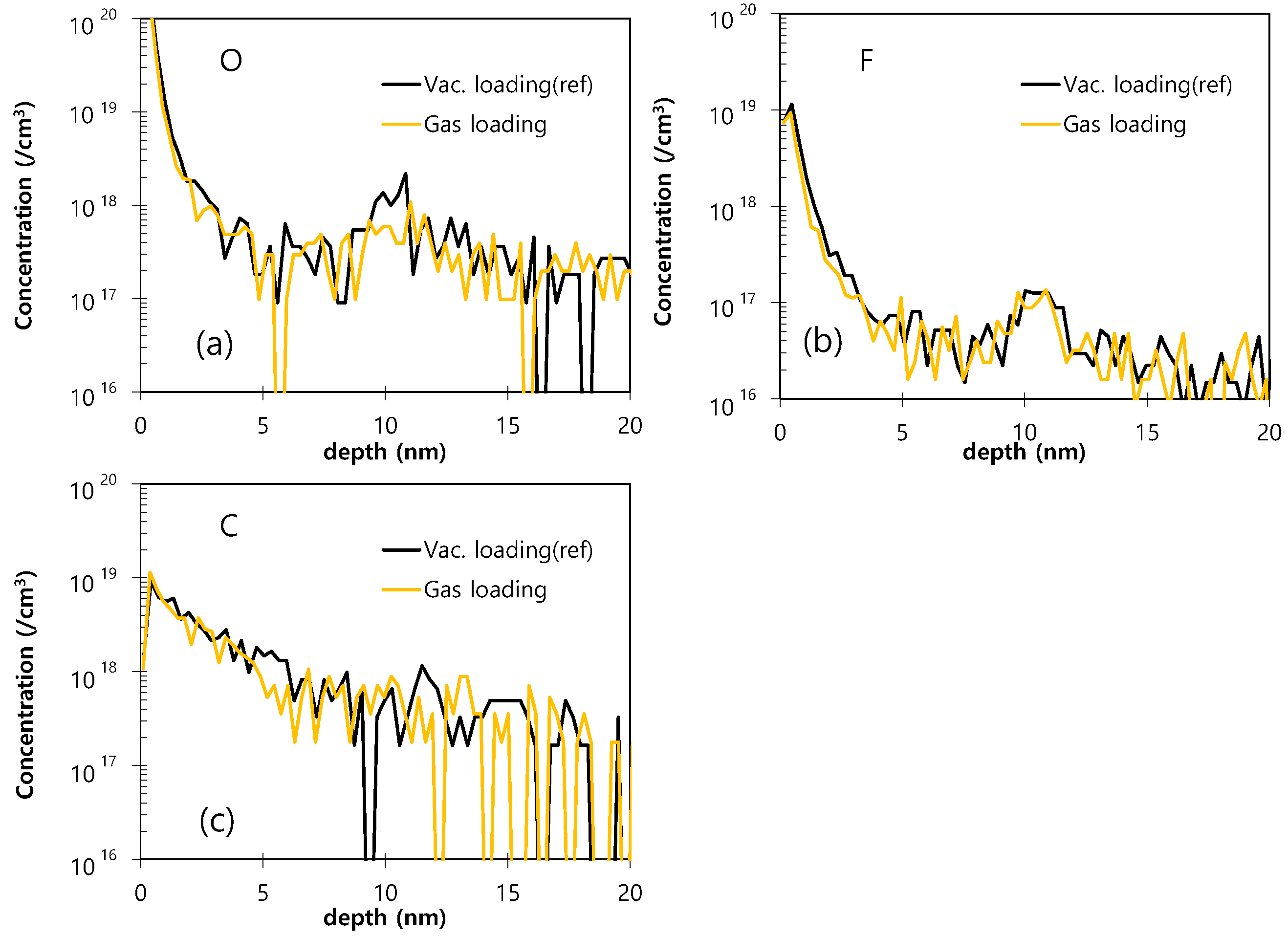
Finally, the SIMS O, F, and C profiles of the Si epitaxial films obtained using different loading conditions (vacuum loading or gaseous loading), where all wafers were dry pre-cleaned, are presented in
Figure 12. Here, the O impurity is seen to be suppressed under the gaseous loading environment compared to that observed under the vacuum loading environment. This is explained similarly to the effects of loading temperature (i.e., the gaseous environment in the process chamber at the time of loading the wafer is effective for preserving the Si–H bonding on the surface of the Si wafer).
4. Conclusions
The present study examined the effects of three main epitaxy steps (ex-situ cleaning, in-situ bake and the wafer loading environment) upon the quality of Si-based epitaxial films obtained via reduced pressure chemical vapor deposition (RPCVD). With respect to ex-situ cleaning, dry cleaning gave better results than either wet cleaning with a 1:200 solution of dilute hydrofluoric acid (DHF) in deionized water or wet cleaning with 1:30 DHF. However, the best cleaning effect of all was obtained using a combination of wet (1:200 DHF) and dry cleaning. A multi-stack consisting of Si/SiGe/Si on a Si substrate grown after wet pre-cleaning (200:1 DHF) and H2 bake at 700 °C showed strained-pseudomorphic layers by HRXRD. With respect to the in-situ H2 bake, the levels of oxygen and fluorine impurities were found to decrease as the temperature increased from 700 to 800 °C, and no impurities peaks were observed at a bake temperature of 850 °C. Moreover, an additional baking step in HCl after the H2 bake was effective even at a temperature as low as 700 °C. Finally, with respect to the conditions of the process chamber at the time of loading the wafers, loading under a gaseous atmosphere at lower temperature gave better epitaxial film quality.
These results provide a valuable guideline for high-quality, low-temperature epitaxial growth in a cluster RPCVD system. The recommended steps should be carefully applied in to avoid compromising the quality and throughput of the epitaxy equipment as each step is closely related to the epitaxy throughput.
Author Contributions
Conceptualization, J.J., B.S., B.K., W.-J.L., Y.S.J. and S.P.; methodology, B.S. and B.K.; formal analysis, W.J. and J.J.; investigation, J.J., B.S., B.K., Y.S.J., S.C., W.-J.L. and S.P.; writing—original draft preparation, J.J.; writing—review and editing, J.J.; supervision, B.S., B.K., Y.S.J. and S.P. All authors have read and agreed to the published version of the manuscript.
Funding
This work was supported by the Ministry of Trade, Industry and Energy with the Korea Semiconductor Research Consortium Support Program for the development of the future semiconductor devices (10052928) and by National Research Foundation of Korea (NRF) funded by the Ministry of science, ICT and Future Planning (2020R1A6A1A03043435).
Institutional Review Board Statement
Not applicable.
Informed Consent Statement
Not applicable.
Data Availability Statement
Data sharing is not applicable to this article.
Acknowledgments
Authors would like to thank Park, Yun Chang (National nano fab center (NNFC) TEAM, Korea) for supporting TEM analysis.
Conflicts of Interest
The authors declare no conflict of interest.
References
- Roy, F.; Suler, A.; Dalleau, T.; Duru, R.; Benoit, D.; Arnaud, J.; Cazaux, Y.; Chaton, C.; Montes, L.; Morfouli, P.; et al. Fully Depleted, Trench-Pinned Photo Gate for CMOS Image Sensor Applications. Sensors 2020, 20, 727. [Google Scholar] [CrossRef] [PubMed] [Green Version]
- Chang, H.-R.; Temple, V. High quality thick epitaxial films for power semiconductor devices. Solid State Electron. 1986, 29, 39–46. [Google Scholar] [CrossRef]
- Loubet, N.; Adam, T.; Raymond, M.; Liu, Q.; Cheng, K.; Sreenivasan, R.; Reznicek, A.; Khare, P.; Kleemeier, W.; Paruchuri, V.; et al. Ultra-low resistivity in-situ phosphorus doped Si and SiC epitaxy for source/drain formation in advanced 20nm n-type field effect transistor devices. Thin Solid Films 2012, 520, 3149–3154. [Google Scholar] [CrossRef]
- Li, X.; Dube, A.; Ye, Z.; Sharma, S.; Kim, Y.; Chu, S. Selective Epitaxial Si:P Film for nMOSFET Application: High Phosphorous Concentration and High Tensile Strain. ECS Trans. 2014, 64, 959–965. [Google Scholar] [CrossRef]
- Wu, H.; Gluschenkov, O.; Tsutsui, G.; Niu, C.; Brew, K.; Durfee, C.; Prindle, C.; Kamineni, V.; Mochizuki, S.; Lavoie, C.; et al. Parasitic Resistance Reduction Strategies for Advanced CMOS FinFETs Beyond 7nm. In Proceedings of the 2018 IEEE International Electron Devices Meeting (IEDM), San Francisco, CA, USA, 1–5 December 2018; pp. 35.4.1–35.4.4. [Google Scholar] [CrossRef]
- Myronov, M.; Shah, V.A.; Rhead, S.; Leadley, D.R. Epitaxial Growth of Tensile Strained SiB Alloy on a Si Substrate. In Proceedings of the 2012 International Silicon-Germanium Technology and Device Meeting (ISTDM), Berkeley, CA, USA, 4–6 June 2012; pp. 1–2. [Google Scholar] [CrossRef]
- Thompson, S.; Armstrong, M.; Auth, C.; Alavi, M.; Buehler, M.; Chau, R.; Cea, S.; Ghani, T.; Glass, G.; Hoffman, T.; et al. A 90-nm Logic Technology Featuring Strained-Silicon. IEEE Trans. Electron. Devices 2004, 51, 1790–1797. [Google Scholar] [CrossRef]
- Hashemi, P.; Kobayashi, M.; Majumdar, A.; Yang, L.A.; Baraskar, A.; Balakrishnan, K.; Kim, K.; Chan, K.; Engelmann, S.U.; Ott, J.A.; et al. High-performance Si1−xGex channel on insulator trigate PFETs featuring an implant-free process and aggressively-scaled fin and gate dimensions. In Proceedings of the 2013 Symposium on VLSI Circuits, Kyoto, Japan, 12–14 June 2013; pp. T18–T19. [Google Scholar]
- Vincent, B.; Witters, L.; Richard, O.; Hikavyy, A.; Bender, H.; Loo, R.; Caymax, M.; Thean, A. Selective Growth of Strained Ge Channel on Relaxed SiGe Buffer in Shallow Trench Isolation for High Mobility Ge Planar and Fin p-FET. ECS Trans. 2013, 50, 39–45. [Google Scholar] [CrossRef]
- Delhougne, R.; Eneman, G.; Caymax, M.; Loo, R.; Meunier-Beillard, P.; Verheyen, P.; Vandervorst, W.; De Meyer, K.; Heyns, M. Selective epitaxial deposition of strained silicon: A simple and effective method for fabricating high performance MOSFET devices. Solid State Electron. 2004, 48, 1307–1316. [Google Scholar] [CrossRef]
- Lee, M.; Antoniadis, D.; Fitzgerald, E. Strained and Relaxed SiGe for High-Mobility MOSFETs. In Proceedings of the 2006 International SiGe Technology and Device Meeting, Princeton, NJ, USA, 15–17 May 2006; pp. 1–2. [Google Scholar] [CrossRef]
- Barraud, S.; Lapras, V.; Previtali, B.; Samson, M.P.; Lacord, J.; Martinie, S.; Jaud, M.-A.; Athanasiou, S.; Triozon, F.; Rozeau, O.; et al. Performance and design considerations for gate-all-around stacked-NanoWires FETs. In Proceedings of the 2017 IEEE International Electron Devices Meeting (IEDM), San Francisco, CA, USA, 2–6 December 2017; pp. 29.2.1–29.2.4. [Google Scholar] [CrossRef] [Green Version]
- Thomas, S. Gate-all-around transistors stack up. Nat. Electron. 2020, 3, 728. [Google Scholar] [CrossRef]
- Glowacki, F.; Campidelli, Y. Single wafer epitaxy of Si and SiGe using UHV-CVD. Microelectron. Eng. 1994, 25, 161–170. [Google Scholar] [CrossRef]
- He, H.; Brabant, P.; Chung, K.; Shinriki, M.; Adam, T.; Reznicek, A.; Sadana, D.; Hasaka, S.; Francis, T. High strain embedded-SiGe via low temperature reduced pressure chemical vapor deposition. Thin Solid Films 2012, 520, 3175–3178. [Google Scholar] [CrossRef]
- Hartmann, J.M.; Loup, V.; Rolland, G.; Holliger, P.; Laugier, F.; Vannuffel, C.; Séméria, M.N. SiGe growth kinetics and doping in reduced pressure-chemical vapor deposition. J. Cryst. Growth 2002, 236, 10–20. [Google Scholar] [CrossRef]
- Sedgwick, T.O.; Agnello, P.D.; Berkenblit, M.; Kuan, T.S. Growth of Facet-Free Selective Silicon Epitaxy at Low Temperature and Atmospheric Pressure. J. Electrochem. Soc. 1991, 138, 3042–3047. [Google Scholar] [CrossRef]
- Destefanis, V.; Hartmann, J.M.; Hopstaken, M.; Delaye, V.; Bensahel, D. Low-thermal surface preparation, HCl etch and Si/SiGe selective epitaxy on (110) silicon surfaces. Semicond. Sci. Technol. 2008, 23. [Google Scholar] [CrossRef]
- Cheng, P.L.; Liao, C.I.; Wu, H.R.; Chen, Y.C.; Chien, C.C.; Yang, C.L.; Yang, S.F.; Tzou, J.; Tang, R.; Kodali, L.; et al. Effective surface treatments for selective epitaxial SiGe growth in locally strained pMOSFETs. Semicond. Sci. Technol. 2007, 22, S140–S143. [Google Scholar] [CrossRef] [Green Version]
- Kormann, T.; Garnier, P.; Chabanne, G.; Fortuin, A. Ex-situ wet clean and in-situ hydrogen clean for Si and SiGe epitaxy. Thin Solid Films 2008, 517, 269–271. [Google Scholar] [CrossRef]
- Loo, R.; Hikavyy, A.; Leys, F.E.; Wada, M.; Sano, K.; De Vos, B.; Pacco, A.; Gonzalez, M.B.; Simoen, E.; Verheyen, P.; et al. Low Temperature Pre-Epi Treatment: Critical Parameters to Control Interface Contamination. Solid State Phenom. 2009, 145–146, 177–180. [Google Scholar] [CrossRef]
- Abbadie, A.; Hartmann, J.; Holliger, P.; Semeria, M.; Besson, P.; Gentile, P. Low thermal budget surface preparation of Si and SiGe. Appl. Surf. Sci. 2004, 225, 256–266. [Google Scholar] [CrossRef]
- Wang, J.; Inokuchi, Y.; Kunii, Y. Low-Temperature Pre-Treatments in Vertical Epitaxial Reactor with Improved Vacuum Load-Lock Chamber. In Proceedings of the 2006 International SiGe Technology and Device Meeting, Princeton, NJ, USA, 15–17 May 2006; Volume 22, pp. S107–S109. [Google Scholar]
- Vincent, B.; Loo, R.; Vandervorst, W.; Brammertz, G.; Caymax, M. Low temperature Si homo-epitaxy by reduced pressure chemical vapor deposition using dichlorosilane, silane and trisilane. J. Cryst. Growth 2010, 312, 2671–2676. [Google Scholar] [CrossRef]
- Porret, C.; Hikavyy, A.Y.; Granados, J.F.G.; Baudot, S.; Vohra, A.; Kunert, B.; Douhard, B.; Bogdanowicz, J.; Schaekers, M.; Kohen, D.; et al. (Invited) Very Low Temperature Epitaxy of Group-IV Semiconductors for Use in Finfet, Stacked Nanowires and Monolithic 3D Integration. ECS J. Solid State Sci. Technol. 2019, 8, 392. [Google Scholar] [CrossRef]
- Hartmann, J.; Benevent, V.; Damlencourt, J.; Billon, T. A benchmarking of silane, disilane and dichlorosilane for the low temperature growth of group IV layers. Thin Solid Films 2012, 520, 3185–3189. [Google Scholar] [CrossRef]
- Arkles, B.; Pan, Y.; Jove, F.; Goff, J.; Kaloyeros, A. Synthesis and Exploratory Deposition Studies of Isotetrasilane and Reactive Intermediates for Epitaxial Silicon. Inorg. Chem. 2019, 58, 3050–3057. [Google Scholar] [CrossRef] [PubMed] [Green Version]
- Finch, R.H.; Queisser, H.J.; Thomas, G.; Washburn, J. Structure and Origin of Stacking Faults in Epitaxial Silicon. J. Appl. Phys. 1963, 34, 406. [Google Scholar] [CrossRef]
- Kern, W. Handbook of Semiconductor Wafer Cleaning Technology: Science, Technology, and Applications; Noyes Publications: Park Ridge, NJ, USA, 1993. [Google Scholar]
- Ramadan, Z.; Abdelmotalib, H.M.; Im, I.-T.; Im, I. Modeling of Epitaxial Silicon Growth from the DCS-H2-HCl System in a Large Scale CVD Reactor. IEEE Trans. Semicond. Manuf. 2018, 31, 363–370. [Google Scholar] [CrossRef]
- Ramadan, Z.; Im, I.-T. Optimization of Operating Parameters in a Planetary CVD Reactor Using Response Surface Methodology. Silicon 2019, 11, 2067–2074. [Google Scholar] [CrossRef]
- Kuijer, T.; Giling, L.; Bloem, J. Gas phase etching of silicon with HCl. J. Cryst. Growth 1974, 22, 29–33. [Google Scholar] [CrossRef]
Figure 1.
Basic schematic of epitaxial process flow using a reduced pressure chemical vapor deposition (RPCVD) tool.
Figure 1.
Basic schematic of epitaxial process flow using a reduced pressure chemical vapor deposition (RPCVD) tool.
Figure 2.
The secondary ion mass spectroscopy (SIMS) profiles of the SiGe epitaxial films obtained after pre-cleaning with 1:30 DHF and 1:200 DHF, indicating the concentrations of (a) O and (b) F.
Figure 2.
The secondary ion mass spectroscopy (SIMS) profiles of the SiGe epitaxial films obtained after pre-cleaning with 1:30 DHF and 1:200 DHF, indicating the concentrations of (a) O and (b) F.
Figure 3.
The SIMS profiles of the Si epitaxial films obtained after ex-situ wet pre-cleaning with 1:200 DHF, dry cleaning, and combined wet + dry cleaning, indicating the concentrations of (a) O, (b) F, and (c) C.
Figure 3.
The SIMS profiles of the Si epitaxial films obtained after ex-situ wet pre-cleaning with 1:200 DHF, dry cleaning, and combined wet + dry cleaning, indicating the concentrations of (a) O, (b) F, and (c) C.
Figure 4.
The TEM images of the Si epitaxial films obtained after ex-situ pre-cleaning with inset of HRTEM image (a) with 1:200 DHF (wet clean only), (b) dry clean only, and (c) wet + dry cleaning.
Figure 4.
The TEM images of the Si epitaxial films obtained after ex-situ pre-cleaning with inset of HRTEM image (a) with 1:200 DHF (wet clean only), (b) dry clean only, and (c) wet + dry cleaning.
Figure 5.
The SIMS O (a) and F (b) profiles of the Si epitaxial films obtained after wet pre-cleaning and subsequent H2 bake at various temperatures; (c) a bar chart showing the corresponding areal doses of O and F. (700 °C for 10 min, 750, 800, 850 °C for 5 min).
Figure 5.
The SIMS O (a) and F (b) profiles of the Si epitaxial films obtained after wet pre-cleaning and subsequent H2 bake at various temperatures; (c) a bar chart showing the corresponding areal doses of O and F. (700 °C for 10 min, 750, 800, 850 °C for 5 min).
Figure 6.
The TEM images of the Si epitaxial films obtained after wet pre-cleaning and subsequent H2 bake at various temperatures. (a) 700 °C for 10 min, (b–d) 750, 800, 850 °C for 5 min.
Figure 6.
The TEM images of the Si epitaxial films obtained after wet pre-cleaning and subsequent H2 bake at various temperatures. (a) 700 °C for 10 min, (b–d) 750, 800, 850 °C for 5 min.
Figure 7.
The TEM image of the epi-Si obtained after wet pre-cleaning and subsequent H2 bake at 750 °C 5 min. (a) TEM image, (b) TEM image of the red box, (c) FFTs of substrate and epitaxial layer showing crystalline structure.
Figure 7.
The TEM image of the epi-Si obtained after wet pre-cleaning and subsequent H2 bake at 750 °C 5 min. (a) TEM image, (b) TEM image of the red box, (c) FFTs of substrate and epitaxial layer showing crystalline structure.
Figure 8.
The TEM image and high resolution X-ray diffraction (HRXRD) of the Si (10 nm)/SiGe (14 nm)/Si (6 nm) epitaxial films obtained after wet pre-cleaning and subsequent H2 bake at 700 °C. (a) TEM image (b) HRXRD rocking curve (Si and SiGe peaks are shown).
Figure 8.
The TEM image and high resolution X-ray diffraction (HRXRD) of the Si (10 nm)/SiGe (14 nm)/Si (6 nm) epitaxial films obtained after wet pre-cleaning and subsequent H2 bake at 700 °C. (a) TEM image (b) HRXRD rocking curve (Si and SiGe peaks are shown).
Figure 9.
The SIMS O (a) and F (b) profiles of the Si epitaxial films obtained after dry pre-cleaning and subsequent H2 bake at various temperatures.
Figure 9.
The SIMS O (a) and F (b) profiles of the Si epitaxial films obtained after dry pre-cleaning and subsequent H2 bake at various temperatures.
Figure 10.
The SIMS O (a), F (b), and C (c) profiles of the Si epitaxial films obtained after ex-situ dry pre-cleaning and subsequent in-situ bake in the presence of H2 and then HCl at 700 °C.
Figure 10.
The SIMS O (a), F (b), and C (c) profiles of the Si epitaxial films obtained after ex-situ dry pre-cleaning and subsequent in-situ bake in the presence of H2 and then HCl at 700 °C.
Figure 11.
The SIMS O (a) and F (b) profiles of the Si epitaxial films obtained under various loading temperatures using samples that were dry pre-cleaned.
Figure 11.
The SIMS O (a) and F (b) profiles of the Si epitaxial films obtained under various loading temperatures using samples that were dry pre-cleaned.
Figure 12.
The SIMS O (a), F (b), and C (c) profiles of the Si epitaxial films obtained using different loading conditions (vacuum loading or gaseous loading), where all wafers were dry pre-cleaned.
Figure 12.
The SIMS O (a), F (b), and C (c) profiles of the Si epitaxial films obtained using different loading conditions (vacuum loading or gaseous loading), where all wafers were dry pre-cleaned.
| Publisher’s Note: MDPI stays neutral with regard to jurisdictional claims in published maps and institutional affiliations. |
© 2021 by the authors. Licensee MDPI, Basel, Switzerland. This article is an open access article distributed under the terms and conditions of the Creative Commons Attribution (CC BY) license (https://creativecommons.org/licenses/by/4.0/).


 ,
, 