Article

Monolayer Twisted Graphene-Based Schottky Transistor

by
Ramin Ahmadi
1,
Mohammad Taghi Ahmadi
1,*,
Seyed Saeid Rahimian Koloor
2,* and
Michal Petrů
3
1
Nano-Physics Group, Nano-Technology Research Center, Physics Department, Faculty of Science, Urmia University, Urmia 5756151818, Iran
2
Institute for Nanomaterials, Advanced Technologies and Innovation (CXI), Technical University of Liberec (TUL), Studentska 2, 461-17 Liberec, Czech Republic
3
Technical University of Liberec (TUL), Studentska 2, 461-17 Liberec, Czech Republic
*
Authors to whom correspondence should be addressed.
Materials 2021, 14(15), 4109; https://doi.org/10.3390/ma14154109
Submission received: 13 June 2021 / Revised: 9 July 2021 / Accepted: 17 July 2021 / Published: 23 July 2021

Abstract

:
The outstanding properties of graphene-based components, such as twisted graphene, motivates nanoelectronic researchers to focus on their applications in device technology. Twisted graphene as a new class of graphene structures is investigated in the platform of transistor application in this research study. Therefore, its geometry effect on Schottky transistor operation is analyzed and the relationship between the diameter of twist and number of twists are explored. A metal–semiconductor–metal twisted graphene-based junction as a Schottky transistor is considered. By employing the dispersion relation and quantum tunneling the variation of transistor performance under channel length, the diameter of twisted graphene, and the number of twists deviation are studied. The results show that twisted graphene with a smaller diameter affects the efficiency of twisted graphene-based Schottky transistors. Additionally, as another main characteristic, the ID-VGS is explored, which indicates that the threshold voltage is increased by diameter and number of twists in this type of transistor.

1. Introduction

In the last decade, most efforts of nanotechnology researchers have been devoted to the study and characterization of electronic properties of graphene [1,2,3,4,5,6,7]. Indeed, graphene is a two-dimensional honeycomb structure with high electron mobility and stable lattice which has different classifications [8,9,10,11], such as graphene nanoscroll, twisted graphene, graphene nanoribbon, and few-layer graphene [12,13,14,15,16,17]. Among these different types of graphene, twisted graphene is a new class and interesting [18]. Figure 1 shows how the graphene twist is formed from graphene. Different methods, such as stacking of two single-layer graphenes (SLG) [19], cutting-rotation-stacking (CRS) technique of SLG [20], control folding of SLG [21], selective pick-up and transfer of SLG [22], CVD using decaborane on Copper foil [23] and joule heating of polyaromatic hydrocarbons (PAHs) on Nickel foil [24], have been reported for the synthesis of twisted graphene. Edge shapes of twisted graphene are divided into two types: either zigzag or armchair, and each type has a significant role in electronic properties, which are identified by pair of (n, m). The n and m are important coefficients in the chiral vector.
In the zigzag edge, the pairs are converted to (n, 0). Based on this theory, (22, 0), (28, 0) and (34, 0) are metallic, since (n − 1) is a multiple of three, and hence (30, 0), (39, 0) and (45, 0) are semiconducting. These different features of twisted graphene lead to great attention from researchers.
Considering this variety of properties, twisted graphene can be used in different areas of nanoelectronic components such as diodes and transistors. In the present study, a Schottky transistor based on twisted graphene is modeled. Figure 2 indicates the schematic design of the proposed transistor by assuming metallic and semiconducting twisted graphene. The geometry of twisted graphene is analytically modeled. Essential characteristics for the performance of transistors are also discussed.

2. Analytical Modeling

To investigate the electronic properties of twisted graphene, the dispersion relation based on the geometrical effect of twisted graphene should be studied. The graphene sheet has two perpendicular vectors called translation (T) and chiral (C) vectors as shown in Figure 1. T and C vectors are defined as:
C = n a 1 + m a 2 = ( n , m )
and
T = t 1 a 1 + t 2 a 2 = ( t 1 , t 2 )
where a1 and a2 are the basic vectors:
( a 1 = 3 a c c ( 3 2 i + 0.5 j ) and a 2 = 3 a c c ( 3 2 i 0.5 j )
The n and m are integer numbers and ac-c is the C-C bond length. The t1 and t2 are obtained based on the perpendicular property of T and C:
t 1 = 2 m + n d R and t 2 = 2 n + m d R
where dR is:
d R = gcd ( 2 n + m , 2 m + n )
Since the translation vector is parallel to the twist axis, it is equal to the length of twist circumference [25]:
L = | T |
On the other hand, for the length of twist graphene, we have:
L = π z s
where Z is the diameter of the twist and S is the number of twists in twisted graphene. Hence, for any zigzag vector C (n, 0), we have:
T = a 1 2 a 2 = 3
Consequently, using various values of S, the diameter of twist can be obtained as:
z = 3 π s
In the other words, it means that Z is proportional to:
z 1 2 s
Figure 3 confirms the fact that when the number of twists is greater, the diameter of the twist is smaller, and vice versa.
Now, the electronic properties of graphene twist are surveyed. Using the Taylor expansion series, the E-K relation of graphene band structure can be given by [26]:
E = 3 t a C C 2 K x 2 + β 2
Using some simplification, we have:
E = E c + E c 4 β 2 K 2
where Ec is assumed as [27]:
E c = 0.5 t + 3 L 2 2 n 2
Consequently, the amount of β is:
β = t n 2 a + 3 a L 2 3 t n 2 a 2
Based on our proposed structure in Figure 2, the quantum tunneling effect for the Schottky barrier must be regarded. First, the transmission probability in two regions that wave vector changes from K1 to K2 should be calculated. Figure 4 indicates a sketch of Schottky contacts that K1 is the wave vector in the metallic region, K2 is the wave vector in the semiconducting region and L′ is the length of the barrier. The transmission probability (T (E)) is given by [28]:
T ( E ) = ( 1 + ( K 1 2 + K 2 2 2 K 1 K 2 ) 2 sinh 2 ( K 2 L ) ) 1
By replacement of wave vectors in each region, we have:
T ( E ) = ( 1 + ( 4 E 3 t a ( t n 1 2 a + 3 a ( π s z ) 2 3 t n 1 2 a 2 ) 2 ( t n 1 2 a + 3 a ( π s z ) 2 3 t n 1 2 a 2 ) 2 + 4 E 3 t a ( t n 2 2 a + 3 a ( π s z ) 2 3 t n 2 2 a 2 ) 2 ( t n 2 2 a + 3 a ( π s z ) 2 3 t n 2 2 a 2 ) 2 2 4 E 3 t a ( t n 1 2 a + 3 a ( π s z ) 2 3 t n 1 2 a 2 ) 2 ( t n 1 2 a + 3 a ( π s z ) 2 3 t n 1 2 a 2 ) 2 4 E 3 t a ( t n 2 2 a + 3 a ( π s z ) 2 3 t n 2 2 a 2 ) 2 ( t n 2 2 a + 3 a ( π s z ) 2 3 t n 2 2 a 2 ) 2 ) 2 × sinh 2 ( L 4 E 3 t a ( t n 2 2 a + 3 a ( π s z ) 2 3 t n 2 2 a 2 ) 2 ( t n 2 2 a + 3 a ( π s z ) 2 3 t n 2 2 a 2 ) 2 ) ) 1
The geometry effect in (16) can also be seen. Now, by applying a voltage V to the gate of Schottky transistor, the quantum current density (J) can be calculated as in [26,28]:
J = e 2 π V a p p l i e d T ( E )
Consequently, by knowing that the current density definition in 1-D materials, Equation (17) is converted to:
I = e 2 π L V a p p l i e d T ( E )
The applied voltage is given by:
V a p p = ( ( ( V G S V T ) V D S V D S 2 2 ) + V T )
Where V T is the thermal voltage (26 mV). So, the I-V characteristic relation is obtained by (20):
I = e 2 π L ( ( ( V G S V T ) V D S V D S 2 2 ) + V T ) ( 1 + ( 4 E 3 t a ( t n 1 2 a + 3 a ( π s z ) 2 3 t n 1 2 a 2 ) 2 ( t n 1 2 a + 3 a ( π s z ) 2 3 t n 1 2 a 2 ) 2 + 4 E 3 t a ( t n 2 2 a + 3 a ( π s z ) 2 3 t n 2 2 a 2 ) 2 ( t n 2 2 a + 3 a ( π s z ) 2 3 t n 2 2 a 2 ) 2 2 4 E 3 t a ( t n 1 2 a + 3 a ( π s z ) 2 3 t n 1 2 a 2 ) 2 ( t n 1 2 a + 3 a ( π s z ) 2 3 t n 1 2 a 2 ) 2 4 E 3 t a ( t n 2 2 a + 3 a ( π s z ) 2 3 t n 2 2 a 2 ) 2 ( t n 2 2 a + 3 a ( π s z ) 2 3 t n 2 2 a 2 ) 2 ) 2 × sinh 2 ( L 4 E 3 t a ( t n 2 2 a + 3 a ( π s z ) 2 3 t n 2 2 a 2 ) 2 ( t n 2 2 a + 3 a ( π s z ) 2 3 t n 2 2 a 2 ) 2 ) ) 1

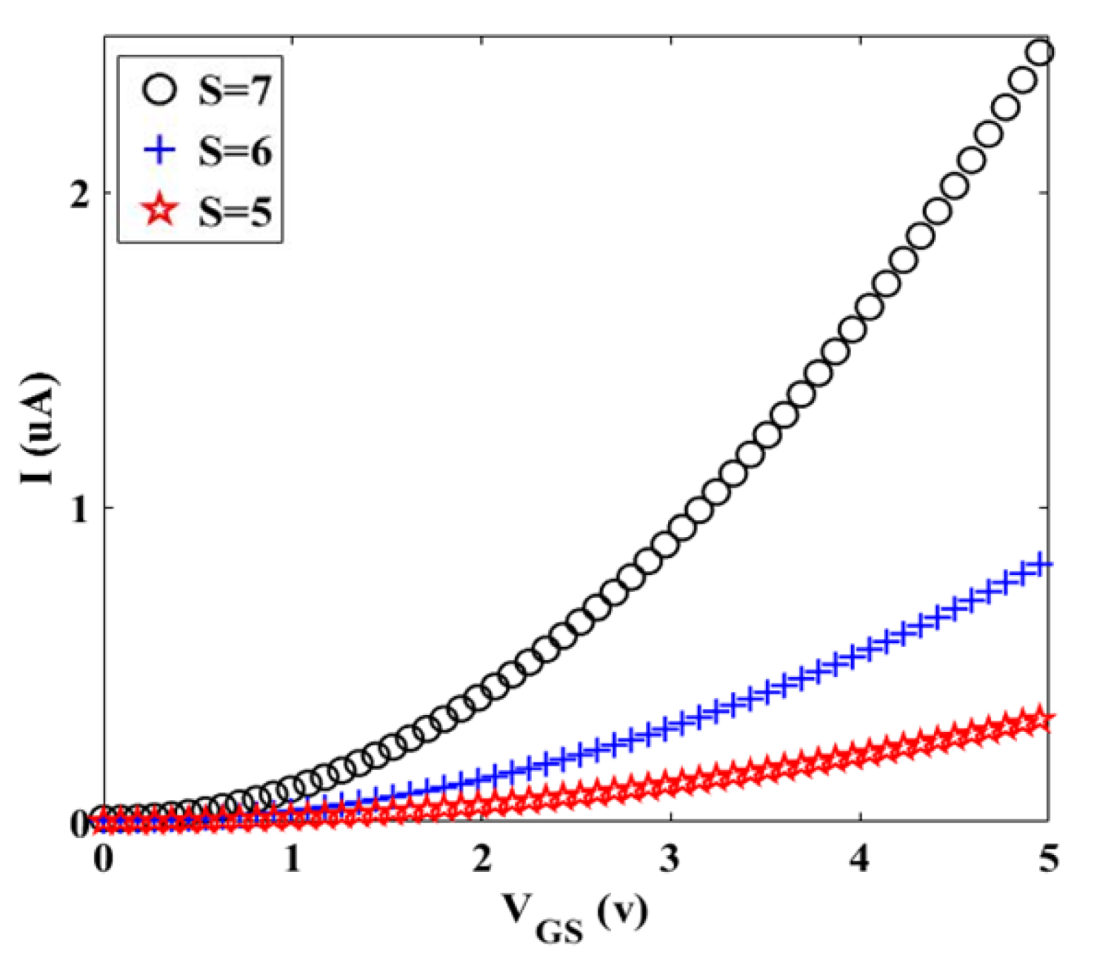
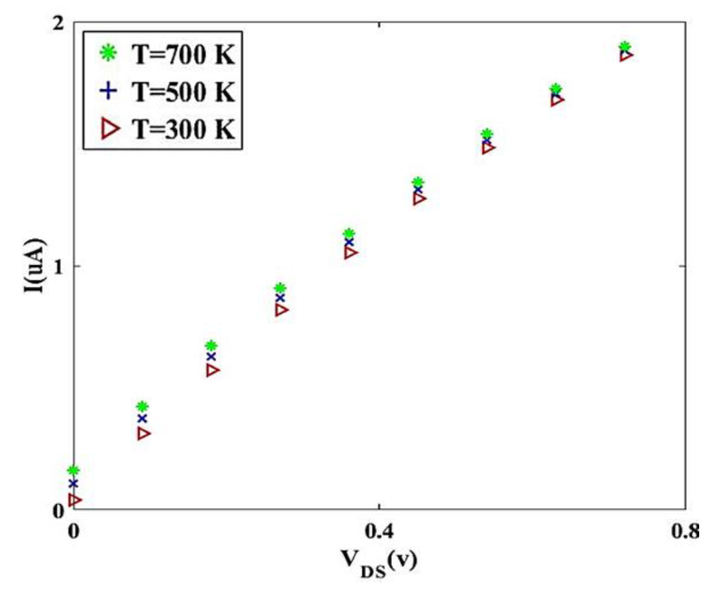
3. Results and Discussion

In this part, the performance of twisted graphene-based Schottky transistor is studied and results, based on the analytical method using MATLAB software, are also discussed. Figure 5 represents the I-VDS at diverse values of VGS. It can be seen that the drain current rises substantially as the gate-source voltage is increased from 0.5 to 1 v which means that the gate-source voltage controls the current in the channel region (ID).
Two factors, which are improving the gate electrostatic control and creating larger transconductance, are as the functions of Schottky transistors channel length [29]. Hence, the current-voltage characteristic for different values of channel length is plotted, as shown in Figure 6. For L′ = 15 nm, it can be said that the electrons move easier than other values of L′ and the tunneling effect not occurred in this case. In the other words, the electron passes through the barrier (moving directly), because the energy of the electron is more than the barrier ( E e V ). Figure 7 and Figure 8 indicate the geometry effect of twisted graphene on I-VDS characteristics. It can be seen from Figure 7 that by adding even one more twist in graphene twist, there is a dramatic descent in the initial slope of ID versus VDS.
It can be discerned from Figure 8 that the I-V characteristic is very sensitive, even to the addition of one nanometer to the diameter of graphene twist, which shows the importance of the Z role in twisted graphene Schottky transistor performance.
Although the S and Z based on Figure 3 have an inverse relation, nevertheless each of them has a reverse effect on transistor performance, which means that increasing in S or Z (separately) leads to the decrease in drain current that is controlled by the gate-source voltage. In the other words, small diameters of twisted graphene led to the transportation of electrons in one dimension, hence, the drain current increases [30]. In fact, the Fermi wavelength (λF) represents that the wavefunctions of carriers that completely fill the diameter of the nanostructure. In the one-dimensional structure that the diameter is smaller than the λF, the electrons in the 1D channel cannot screen the Coulomb potential from the gate and consequently, high current flows and great channel length modulation can be attained [31].
Also, the stress-strain of the twisted structure plays an important role in the variation of different properties [32,33]. Here, when the S is more, the amount of stress-strain of material is higher, and consequently, it leads to some defects in the structure. Defects caused the C-C bonds to break and new barriers to be generated. This phenomenon causes the perturbation of the drain current.
Hence, the drain current decreases. In comparison with Figure 7, in Figure 8, it can be said that even by the selection of larger Z (inset values of Figure 8) compared to amounts of S (inset values of Figure 7), the drain current is more for S, which means that the effect of S is higher than Z on Schottky transistor performance. This is due to the mechanical properties of twisted graphene structure, which means that if the twists (S) are not generated on graphene structure, the Z will not vary. In the other words, Z is a function of S (f(S) = Z). Additionally, in the saturation region, that gradient of ID-VDS characteristic is zero, we have:
V D S ( S A T ) = ( V G S V T )
Therefore, the ID-VGS characteristic for our proposed model can be written as:
I = e 2 π L [ ( V G S V T 2 ) 2 + V T ] T ( E )
Based on this exceptional equation, the threshold voltage of our transistor can be achieved. Figure 9 shows the ID-VGS characteristic for the diverse value of S. To investigate the Z effect on ID-VGS characteristic, Figure 10 is plotted for S = 10.
Figure 9 and Figure 10 illustrate the geometry effect of graphene twist on the threshold voltage of the proposed transistor that increment in the number of twists leads to decrease in threshold voltage of the transistor and it is very good for high-speed switching of transistor, because it causes less transistor power consumption. Figure 10 indicates that the diameter (Z) has an inverse relation on the threshold voltage of the transistor.
To compare Figure 9 and Figure 10, it can be noted that to optimize and improve the performance of twisted graphene Schottky transistor, it is better to choose twisted graphene with a smaller diameter. The temperature effect on transistor performance of twisted graphene is explored for three different amounts using thermal voltage (VT), as shown in Figure 11. Results indicate that increasing temperature leads to an increment in the mobility of electrons in the channel region of the twisted graphene Schottky transistor. Overall current in a real-world device can be lowered also by experimental non-idealities (e.g., contact resistances), which are typically not reflected in simulations.
Finally, a comparative study of our modeled transistor and typical I-V characteristic of other transistors is depicted in Figure 12. In this figure, twisted graphene-based Schottky transistor and graphene nanoscroll-based Schottky transistor [26] in the same situation are considered. It can be noted that the channel length of both Schottky transistors is 60 nm, and they also have the same length of the circumference (L). As indicated in Figure 12, the proposed Schottky transistor has a larger drain current than the graphene nano scroll-based Schottky transistor, and it is a significant advantage for twisted graphene-based Schottky transistor. Additionally, Kosar et al. investigated the geometric, optical, and electronic responses of doped twisted graphene with alkalis and superalkalis in a density functional theory (DFT) study [34]. The differences between our research paper and this work are in the consideration of twisted graphene without any doped material, and also in the methodology of study that is based on tight binding calculations instead of DFT.

4. Conclusions

Twisted graphene with a novel structure is a promising material for nanoelectronic applications due to its remarkable electrical properties. In the presented work, a twisted graphene-based Schottky transistor is analytically modeled. The proposed structure with zigzag twisted graphene as metallic and semiconducting properties depends on its chirality numbers, which are assumed to be (19, 0) and (17, 0), respectively. The geometry of twisted graphene by translation (T) and chiral (C) vectors are explored and the relationship between diameter and number of twists for all zigzag vectors are calculated, considering the dispersion relation and tunneling effect the wave vector changes from K1 to K2 (metallic to semiconducting). By applying a voltage to the proposed structure, the I-V characteristics are studied. It is concluded that increasing the gate-source voltage leads to an increment in drain current. On the other hand, a reduction in diameter and number of twists can increase the drain current. The effect of twisted graphene geometry on the threshold voltage of Schottky transistor indicates that the great number of twists and small values of diameters leads to a low threshold voltage of the transistor. So, it is concluded that in order to promote the performance of twisted graphene-based Schottky transistor, twisted graphene with a small diameter and more number of twists is appropriate. Additionally, the temperature effect on transistor performance is explored, and observations show that temperature increases lead to an increment in the drain current. Finally, the proposed transistor is compared with similar research which represents the superiority of twisted graphene-based Schottky transistor over the graphene nanoscrolls-based Schottky transistor. Altogether, twisted graphene is a desirable nominee for transistor devices in integrated circuits as high-speed switching applications.

Author Contributions

R.A. and M.T.A. designed and performed the device modelling, software and analysis of the data. M.T.A., S.S.R.K. and M.P. supervised the research work and they were the project administrations. R.A., M.T.A., S.S.R.K. and M.P. involved in the investigation, methodology, formal analysis, data curation and validation process of the research content and data. R.A., M.T.A., S.S.R.K. and M.P. drafted, reviewed and proofread the manuscript. M.T.A., S.S.R.K. and M.P. provided the funding for the research. All authors have read and agreed to the published version of the manuscript.

Funding

This research received no external funding.

Institutional Review Board Statement

Not applicable.

Informed Consent Statement

Not applicable.

Data Availability Statement

The data presented in this study are available on reasonable request from the corresponding author.

Acknowledgments

In addition, this research was supported by the Ministry of Education, Youth, and Sports of the Czech Republic and the European Union (European Structural and Investment Funds Operational Program Research, Development, and Education) in the framework of the project “Modular platform for autonomous chassis of specialized electric vehicles for freight and equipment transportation”, Reg. No. CZ.02.1.01/0.0/0.0/16_025/0007293.

Conflicts of Interest

The authors declare no conflict of interest.

References

  1. Rallis, K.; Dimitrakis, P.; Karafyllidis, I.G.; Rubio, A.; Sirakoulis, G.C. Electronic Properties of Graphene Nanoribbons with Defects. IEEE Trans. Nanotechnol. 2021, 20, 151–160. [Google Scholar] [CrossRef]
  2. Koloor, S.S.R.; Rahimian-Koloor, S.; Karimzadeh, A.; Hamdi, M.; Petrů, M.; Tamin, M. Nano-level damage characterization of graphene/polymer cohesive interface under tensile separation. Polymers 2019, 11, 1435. [Google Scholar] [CrossRef] [Green Version]
  3. Hosseingholipourasl, A.; Hafizah Syed Ariffin, S.; Al-Otaibi, Y.D.; Akbari, E.; Hamid, F.; Koloor, S.S.R.; Petrů, M. Analytical Approach to Study Sensing Properties of Graphene Based Gas Sensor. Sensors 2020, 20, 1506. [Google Scholar] [CrossRef] [Green Version]
  4. Molitor, F.; Güttinger, J.; Stampfer, C.; Dröscher, S.; Jacobsen, A.; Ihn, T.; Ensslin, K. Electronic properties of graphene nanostructures. J. Phys. Condens. Matter 2011, 23, 243201. [Google Scholar] [CrossRef] [PubMed]
  5. Khademhosseini, V.; Dideban, D.; Ahmadi, M.; Ismail, R. Current analysis of single electron transistor based on graphene double quantum dots. ECS J. Solid State Sci. Technol. 2020, 9, 021003. [Google Scholar] [CrossRef]
  6. Zoghi, M.; Goharrizi, A.Y. Strain-induced armchair graphene nanoribbon resonant-tunneling diodes. IEEE Trans. Electron Devices 2017, 64, 4322–4326. [Google Scholar] [CrossRef]
  7. Norouzi, M.; Ahmadi, R.; Norian, E.; Ahmadi, M.T.; Ismail, R. The Geometry Variation Effect on Carbon Atom Wire for Nano-Electronic Applications. J. Nanoelectron. Optoelectron. 2019, 14, 1120–1125. [Google Scholar] [CrossRef]
  8. Giubileo, F.; Di Bartolomeo, A. The role of contact resistance in graphene field-effect devices. Progress Surf. Sci. 2017, 92, 143–175. [Google Scholar] [CrossRef] [Green Version]
  9. Akinwande, D.; Huyghebaert, C.; Wang, C.-H.; Serna, M.I.; Goossens, S.; Li, L.-J.; Wong, H.-S.P.; Koppens, F.H. Graphene and two-dimensional materials for silicon technology. Nature 2019, 573, 507–518. [Google Scholar] [CrossRef]
  10. Ahmadi, R.; Ahmadi, M.T.; Ismail, R. Carbon nano-particle synthesized by pulsed arc discharge method as a light emitting device. J. Electron. Mater. 2018, 47, 4003–4009. [Google Scholar] [CrossRef]
  11. Giubileo, F.; Martucciello, N.; Di Bartolomeo, A. Focus on graphene and related materials. Nanotechnology 2017, 28, 410201. [Google Scholar] [CrossRef] [Green Version]
  12. Yang, B.; Chen, J.; Liu, B.; Ding, Y.; Tang, Y.; Yan, X. One dimensional graphene nanoscroll-wrapped MnO nanoparticles for high-performance lithium ion hybrid capacitors. J. Mater. Chem. A 2021, 9, 6352–6360. [Google Scholar] [CrossRef]
  13. Hamzah, A.; Ismail, R. Performance prediction of Graphene Nanoscroll and Carbon Nanotube transistors. In Proceedings of the 2016 IEEE International Conference on Semiconductor Electronics (ICSE), Kuala Lumpur, Malaysia, 17 August 2016; pp. 149–152. [Google Scholar]
  14. He, M.; Li, Y.; Cai, J.; Liu, Y.; Watanabe, K.; Taniguchi, T.; Xu, X.; Yankowitz, M. Symmetry breaking in twisted double bilayer graphene. Nat. Phys. 2021, 17, 26–30. [Google Scholar] [CrossRef]
  15. Da Liao, Y.; Kang, J.; Breiø, C.N.; Xu, X.Y.; Wu, H.-Q.; Andersen, B.M.; Fernandes, R.M.; Meng, Z.Y. Correlation-induced insulating topological phases at charge neutrality in twisted bilayer graphene. Phys. Rev. X 2021, 11, 011014. [Google Scholar]
  16. Saraswat, V.; Jacobberger, R.M.; Arnold, M.S. Materials Science Challenges to Graphene Nanoribbon Electronics. ACS Nano 2021, 15, 3674–3708. [Google Scholar] [CrossRef] [PubMed]
  17. Liang, G.; Neophytou, N.; Lundstrom, M.S.; Nikonov, D.E. Contact effects in graphene nanoribbon transistors. Nano Lett. 2008, 8, 1819–1824. [Google Scholar] [CrossRef]
  18. Mogera, U.; Kulkarni, G.U. A new twist in graphene research: Twisted graphene. Carbon 2020, 156, 470–487. [Google Scholar] [CrossRef]
  19. Robinson, J.T.; Schmucker, S.W.; Diaconescu, C.B.; Long, J.P.; Culbertson, J.C.; Ohta, T.; Friedman, A.L.; Beechem, T.E. Electronic hybridization of large-area stacked graphene films. ACS Nano 2013, 7, 637–644. [Google Scholar] [CrossRef] [Green Version]
  20. Chen, X.D.; Xin, W.; Jiang, W.S.; Liu, Z.B.; Chen, Y.; Tian, J.G. High-Precision Twist-Controlled Bilayer and Trilayer Graphene. Adv. Mater. 2016, 28, 2563–2570. [Google Scholar] [CrossRef]
  21. Wang, B.; Huang, M.; Kim, N.Y.; Cunning, B.V.; Huang, Y.; Qu, D.; Chen, X.; Jin, S.; Biswal, M.; Zhang, X. Controlled folding of single crystal graphene. Nano Lett. 2017, 17, 1467–1473. [Google Scholar] [CrossRef]
  22. Kim, K.; Yankowitz, M.; Fallahazad, B.; Kang, S.; Movva, H.C.; Huang, S.; Larentis, S.; Corbet, C.M.; Taniguchi, T.; Watanabe, K. van der Waals heterostructures with high accuracy rotational alignment. Nano Lett. 2016, 16, 1989–1995. [Google Scholar] [CrossRef] [PubMed]
  23. Liu, J.-B.; Li, P.-J.; Chen, Y.-F.; Wang, Z.-G.; Qi, F.; He, J.-R.; Zheng, B.-J.; Zhou, J.-H.; Zhang, W.-L.; Gu, L. Observation of tunable electrical bandgap in large-area twisted bilayer graphene synthesized by chemical vapor deposition. Sci. Rep. 2015, 5, 1–9. [Google Scholar] [CrossRef] [PubMed] [Green Version]
  24. Mogera, U.; Dhanya, R.; Pujar, R.; Narayana, C.; Kulkarni, G.U. Highly decoupled graphene multilayers: Turbostraticity at its best. J. Phys. Chem. Lett. 2015, 6, 4437–4443. [Google Scholar] [CrossRef] [PubMed]
  25. Dass, D.; Prasher, R.; Vaid, R. Analytical study of unit cell and molecular structures of single walled carbon nanotubes. Int. J. Comput. Eng. Res. 2012, 2, 1447–1457. [Google Scholar]
  26. Ahmadi, M.T.; Ahmadi, R.; Nguyen, T.K. Graphene nanoscroll geometry effect on transistor performance. J. Electron. Mater. 2020, 49, 544–550. [Google Scholar] [CrossRef]
  27. Khaledian, M.; Ismail, R.; Saeidmanesh, M.; Ahmadi, M.; Akbari, E. Carrier statistics and quantum capacitance models of graphene nanoscroll. J. Nanomater. 2014, 2014, 1–6. [Google Scholar] [CrossRef] [Green Version]
  28. Levi, A.F.J. Applied Quantum Mechanics; Cambridge University Press: Cambridge, UK, 2006. [Google Scholar]
  29. Rahmani, M.; Ahmadi, M.T.; Abadi, H.K.F.; Saeidmanesh, M.; Akbari, E.; Ismail, R. Analytical modeling of trilayer graphene nanoribbon Schottky-barrier FET for high-speed switching applications. Nanoscale Res. Lett. 2013, 8, 1–13. [Google Scholar] [CrossRef] [Green Version]
  30. Ismail, R.; Ahmadi, M.T.; Anwar, S. Advanced Nanoelectronics; CRC Press: New York, NY, USA, 2018. [Google Scholar]
  31. Mirza, M.M.; Schupp, F.J.; Mol, J.A.; MacLaren, D.A.; Briggs, G.A.D.; Paul, D.J. One dimensional transport in silicon nanowire junction-less field effect transistors. Sci. Rep. 2017, 7, 1–8. [Google Scholar] [CrossRef] [Green Version]
  32. Liu, A.; Peng, Q. A molecular dynamics study of the mechanical properties of twisted bilayer graphene. Micromachines 2018, 9, 440. [Google Scholar] [CrossRef] [Green Version]
  33. Zheng, S.; Cao, Q.; Liu, S.; Peng, Q. Atomic structure and mechanical properties of twisted bilayer graphene. J. Composites Sci. 2019, 3, 2. [Google Scholar] [CrossRef] [Green Version]
  34. Kosar, N.; Ayub, K.; Mahmood, T. Surface functionalization of twisted graphene C32H15 and C104H52 derivatives with alkalis and superalkalis for NLO response; a DFT study. J. Mol. Graph. Model. 2021, 102, 107794. [Google Scholar] [CrossRef] [PubMed]
Figure 1. The twisted graphene that is achieved from a graphene sheet.
Materials 14 04109 g001
Figure 2. The proposed model.
Materials 14 04109 g002
Figure 3. Z versus S in twisted graphene.
Materials 14 04109 g003
Figure 4. The 1D potential barrier of the proposed twisted graphene Schottky transistor.
Materials 14 04109 g004
Figure 5. I-V characteristic for different values of VGS at room temperature.
Materials 14 04109 g005
Figure 6. I-V characteristic for different values of channel length (in nm) at room temperature (Z = 10 and S = 5).
Materials 14 04109 g006
Figure 7. I-V characteristic for different values of S at room temperature (Z = 10).
Materials 14 04109 g007
Figure 8. I-V characteristic for different values of Z at room temperature (S = 10).
Materials 14 04109 g008
Figure 9. I- VGS characteristic for different values of S at room temperature (Z = 10).
Materials 14 04109 g009
Figure 10. I- VGS characteristic for different values of Z at room temperature (S = 10).
Materials 14 04109 g010
Figure 11. I-V characteristic for diverse values of temperature.
Materials 14 04109 g011
Figure 12. Comparison of the I-V characteristic of our proposed transistor and graphene nanoscroll-based Schottky transistor in the same channel length of 60 nm.
Materials 14 04109 g012
Publisher’s Note: MDPI stays neutral with regard to jurisdictional claims in published maps and institutional affiliations.

